WO2023090133A1 - 合わせガラス及び液晶装置 - Google Patents
合わせガラス及び液晶装置 Download PDFInfo
- Publication number
- WO2023090133A1 WO2023090133A1 PCT/JP2022/040615 JP2022040615W WO2023090133A1 WO 2023090133 A1 WO2023090133 A1 WO 2023090133A1 JP 2022040615 W JP2022040615 W JP 2022040615W WO 2023090133 A1 WO2023090133 A1 WO 2023090133A1
- Authority
- WO
- WIPO (PCT)
- Prior art keywords
- liquid crystal
- covering member
- laminated glass
- light control
- transparent substrate
- Prior art date
Links
- 239000004973 liquid crystal related substance Substances 0.000 title claims abstract description 91
- 239000005340 laminated glass Substances 0.000 title claims abstract description 77
- 239000000758 substrate Substances 0.000 claims abstract description 55
- 210000002858 crystal cell Anatomy 0.000 claims abstract description 37
- 239000000463 material Substances 0.000 claims description 43
- 238000002834 transmittance Methods 0.000 claims description 20
- 230000002093 peripheral effect Effects 0.000 claims description 18
- 210000004027 cell Anatomy 0.000 abstract description 124
- 230000007547 defect Effects 0.000 abstract description 6
- 239000010410 layer Substances 0.000 description 91
- 239000011521 glass Substances 0.000 description 44
- 239000010408 film Substances 0.000 description 30
- 150000001875 compounds Chemical class 0.000 description 24
- 229920005989 resin Polymers 0.000 description 19
- 239000011347 resin Substances 0.000 description 19
- 125000006850 spacer group Chemical group 0.000 description 15
- 239000011324 bead Substances 0.000 description 14
- -1 acryl Chemical group 0.000 description 11
- 239000000975 dye Substances 0.000 description 11
- 239000000203 mixture Substances 0.000 description 11
- XLOMVQKBTHCTTD-UHFFFAOYSA-N Zinc monoxide Chemical compound [Zn]=O XLOMVQKBTHCTTD-UHFFFAOYSA-N 0.000 description 9
- 229920000139 polyethylene terephthalate Polymers 0.000 description 8
- 239000005020 polyethylene terephthalate Substances 0.000 description 8
- 238000004519 manufacturing process Methods 0.000 description 7
- 238000000034 method Methods 0.000 description 7
- 230000000694 effects Effects 0.000 description 6
- 230000003287 optical effect Effects 0.000 description 6
- 239000005357 flat glass Substances 0.000 description 5
- 229920000178 Acrylic resin Polymers 0.000 description 4
- 239000004925 Acrylic resin Substances 0.000 description 4
- 238000010586 diagram Methods 0.000 description 4
- 239000007788 liquid Substances 0.000 description 4
- 239000004417 polycarbonate Substances 0.000 description 4
- 229920000515 polycarbonate Polymers 0.000 description 4
- XOLBLPGZBRYERU-UHFFFAOYSA-N tin dioxide Chemical compound O=[Sn]=O XOLBLPGZBRYERU-UHFFFAOYSA-N 0.000 description 4
- 229910001887 tin oxide Inorganic materials 0.000 description 4
- 239000011787 zinc oxide Substances 0.000 description 4
- 229920000089 Cyclic olefin copolymer Polymers 0.000 description 3
- VYPSYNLAJGMNEJ-UHFFFAOYSA-N Silicium dioxide Chemical compound O=[Si]=O VYPSYNLAJGMNEJ-UHFFFAOYSA-N 0.000 description 3
- 239000012790 adhesive layer Substances 0.000 description 3
- 239000011248 coating agent Substances 0.000 description 3
- 238000000576 coating method Methods 0.000 description 3
- 229910003437 indium oxide Inorganic materials 0.000 description 3
- PJXISJQVUVHSOJ-UHFFFAOYSA-N indium(iii) oxide Chemical compound [O-2].[O-2].[O-2].[In+3].[In+3] PJXISJQVUVHSOJ-UHFFFAOYSA-N 0.000 description 3
- 239000003566 sealing material Substances 0.000 description 3
- 229920002284 Cellulose triacetate Polymers 0.000 description 2
- 239000004986 Cholesteric liquid crystals (ChLC) Substances 0.000 description 2
- 239000004988 Nematic liquid crystal Substances 0.000 description 2
- 239000004698 Polyethylene Substances 0.000 description 2
- 239000004743 Polypropylene Substances 0.000 description 2
- 239000004990 Smectic liquid crystal Substances 0.000 description 2
- 229910006404 SnO 2 Inorganic materials 0.000 description 2
- ISAKRJDGNUQOIC-UHFFFAOYSA-N Uracil Chemical compound O=C1C=CNC(=O)N1 ISAKRJDGNUQOIC-UHFFFAOYSA-N 0.000 description 2
- NNLVGZFZQQXQNW-ADJNRHBOSA-N [(2r,3r,4s,5r,6s)-4,5-diacetyloxy-3-[(2s,3r,4s,5r,6r)-3,4,5-triacetyloxy-6-(acetyloxymethyl)oxan-2-yl]oxy-6-[(2r,3r,4s,5r,6s)-4,5,6-triacetyloxy-2-(acetyloxymethyl)oxan-3-yl]oxyoxan-2-yl]methyl acetate Chemical compound O([C@@H]1O[C@@H]([C@H]([C@H](OC(C)=O)[C@H]1OC(C)=O)O[C@H]1[C@@H]([C@@H](OC(C)=O)[C@H](OC(C)=O)[C@@H](COC(C)=O)O1)OC(C)=O)COC(=O)C)[C@@H]1[C@@H](COC(C)=O)O[C@@H](OC(C)=O)[C@H](OC(C)=O)[C@H]1OC(C)=O NNLVGZFZQQXQNW-ADJNRHBOSA-N 0.000 description 2
- 239000000853 adhesive Substances 0.000 description 2
- 230000001070 adhesive effect Effects 0.000 description 2
- JRXXLCKWQFKACW-UHFFFAOYSA-N biphenylacetylene Chemical group C1=CC=CC=C1C#CC1=CC=CC=C1 JRXXLCKWQFKACW-UHFFFAOYSA-N 0.000 description 2
- 229920002678 cellulose Chemical class 0.000 description 2
- 239000001913 cellulose Chemical class 0.000 description 2
- 229940114081 cinnamate Drugs 0.000 description 2
- ZYGHJZDHTFUPRJ-UHFFFAOYSA-N coumarin Chemical compound C1=CC=C2OC(=O)C=CC2=C1 ZYGHJZDHTFUPRJ-UHFFFAOYSA-N 0.000 description 2
- 230000006866 deterioration Effects 0.000 description 2
- ZUOUZKKEUPVFJK-UHFFFAOYSA-N diphenyl Chemical compound C1=CC=CC=C1C1=CC=CC=C1 ZUOUZKKEUPVFJK-UHFFFAOYSA-N 0.000 description 2
- 230000005684 electric field Effects 0.000 description 2
- 238000005192 partition Methods 0.000 description 2
- 238000011907 photodimerization Methods 0.000 description 2
- 229920002492 poly(sulfone) Polymers 0.000 description 2
- 229920000573 polyethylene Polymers 0.000 description 2
- 229920000642 polymer Polymers 0.000 description 2
- 229920001155 polypropylene Polymers 0.000 description 2
- 238000011176 pooling Methods 0.000 description 2
- 229920002050 silicone resin Polymers 0.000 description 2
- SKRWFPLZQAAQSU-UHFFFAOYSA-N stibanylidynetin;hydrate Chemical compound O.[Sn].[Sb] SKRWFPLZQAAQSU-UHFFFAOYSA-N 0.000 description 2
- 229920002803 thermoplastic polyurethane Polymers 0.000 description 2
- WBYWAXJHAXSJNI-VOTSOKGWSA-M trans-cinnamate Chemical compound [O-]C(=O)\C=C\C1=CC=CC=C1 WBYWAXJHAXSJNI-VOTSOKGWSA-M 0.000 description 2
- IWIOHRVOBOYWQE-UHFFFAOYSA-N (1-cyclohexylcyclohexyl)benzene Chemical group C1CCCCC1C1(C=2C=CC=CC=2)CCCCC1 IWIOHRVOBOYWQE-UHFFFAOYSA-N 0.000 description 1
- FEIQOMCWGDNMHM-KBXRYBNXSA-N (2e,4e)-5-phenylpenta-2,4-dienoic acid Chemical class OC(=O)\C=C\C=C\C1=CC=CC=C1 FEIQOMCWGDNMHM-KBXRYBNXSA-N 0.000 description 1
- YJTKZCDBKVTVBY-UHFFFAOYSA-N 1,3-Diphenylbenzene Chemical group C1=CC=CC=C1C1=CC=CC(C=2C=CC=CC=2)=C1 YJTKZCDBKVTVBY-UHFFFAOYSA-N 0.000 description 1
- UWCWUCKPEYNDNV-LBPRGKRZSA-N 2,6-dimethyl-n-[[(2s)-pyrrolidin-2-yl]methyl]aniline Chemical compound CC1=CC=CC(C)=C1NC[C@H]1NCCC1 UWCWUCKPEYNDNV-LBPRGKRZSA-N 0.000 description 1
- BIAWAXVRXKIUQB-MDZDMXLPSA-N 2-[(e)-2-phenylethenyl]pyridine Chemical compound C=1C=CC=CC=1/C=C/C1=CC=CC=N1 BIAWAXVRXKIUQB-MDZDMXLPSA-N 0.000 description 1
- OXPDQFOKSZYEMJ-UHFFFAOYSA-N 2-phenylpyrimidine Chemical class C1=CC=CC=C1C1=NC=CC=N1 OXPDQFOKSZYEMJ-UHFFFAOYSA-N 0.000 description 1
- GOLORTLGFDVFDW-UHFFFAOYSA-N 3-(1h-benzimidazol-2-yl)-7-(diethylamino)chromen-2-one Chemical compound C1=CC=C2NC(C3=CC4=CC=C(C=C4OC3=O)N(CC)CC)=NC2=C1 GOLORTLGFDVFDW-UHFFFAOYSA-N 0.000 description 1
- NLHHRLWOUZZQLW-UHFFFAOYSA-N Acrylonitrile Chemical compound C=CC#N NLHHRLWOUZZQLW-UHFFFAOYSA-N 0.000 description 1
- 239000005264 High molar mass liquid crystal Substances 0.000 description 1
- 235000000177 Indigofera tinctoria Nutrition 0.000 description 1
- NAACPBBQTFFYQB-UHFFFAOYSA-N Linolsaeure-cholesterylester Natural products C12CCC3(C)C(C(C)CCCC(C)C)CCC3C2CC=C2C1(C)CCC(OC(=O)CCCCCCCC=CCC=CCCCCC)C2 NAACPBBQTFFYQB-UHFFFAOYSA-N 0.000 description 1
- PEEHTFAAVSWFBL-UHFFFAOYSA-N Maleimide Chemical compound O=C1NC(=O)C=C1 PEEHTFAAVSWFBL-UHFFFAOYSA-N 0.000 description 1
- RJECHNNFRHZQKU-UHFFFAOYSA-N Oelsaeurecholesterylester Chemical class C12CCC3(C)C(C(C)CCCC(C)C)CCC3C2CC=C2C1(C)CCC(OC(=O)CCCCCCCC=CCCCCCCCC)C2 RJECHNNFRHZQKU-UHFFFAOYSA-N 0.000 description 1
- 229920008285 Poly(ether ketone) PEK Polymers 0.000 description 1
- 229920012266 Poly(ether sulfone) PES Polymers 0.000 description 1
- 239000004721 Polyphenylene oxide Substances 0.000 description 1
- 239000004793 Polystyrene Substances 0.000 description 1
- 229920001328 Polyvinylidene chloride Polymers 0.000 description 1
- KWYUFKZDYYNOTN-UHFFFAOYSA-M Potassium hydroxide Chemical compound [OH-].[K+] KWYUFKZDYYNOTN-UHFFFAOYSA-M 0.000 description 1
- 239000004820 Pressure-sensitive adhesive Substances 0.000 description 1
- CZPWVGJYEJSRLH-UHFFFAOYSA-N Pyrimidine Chemical compound C1=CN=CN=C1 CZPWVGJYEJSRLH-UHFFFAOYSA-N 0.000 description 1
- CDBYLPFSWZWCQE-UHFFFAOYSA-L Sodium Carbonate Chemical compound [Na+].[Na+].[O-]C([O-])=O CDBYLPFSWZWCQE-UHFFFAOYSA-L 0.000 description 1
- DPOPAJRDYZGTIR-UHFFFAOYSA-N Tetrazine Chemical compound C1=CN=NN=N1 DPOPAJRDYZGTIR-UHFFFAOYSA-N 0.000 description 1
- SMEGJBVQLJJKKX-HOTMZDKISA-N [(2R,3S,4S,5R,6R)-5-acetyloxy-3,4,6-trihydroxyoxan-2-yl]methyl acetate Chemical compound CC(=O)OC[C@@H]1[C@H]([C@@H]([C@H]([C@@H](O1)O)OC(=O)C)O)O SMEGJBVQLJJKKX-HOTMZDKISA-N 0.000 description 1
- 238000009825 accumulation Methods 0.000 description 1
- 229940081735 acetylcellulose Drugs 0.000 description 1
- 239000000654 additive Substances 0.000 description 1
- 230000000996 additive effect Effects 0.000 description 1
- PYKYMHQGRFAEBM-UHFFFAOYSA-N anthraquinone Natural products CCC(=O)c1c(O)c2C(=O)C3C(C=CC=C3O)C(=O)c2cc1CC(=O)OC PYKYMHQGRFAEBM-UHFFFAOYSA-N 0.000 description 1
- 150000004056 anthraquinones Chemical class 0.000 description 1
- 125000000751 azo group Chemical group [*]N=N[*] 0.000 description 1
- 235000010290 biphenyl Nutrition 0.000 description 1
- 239000004305 biphenyl Substances 0.000 description 1
- 239000005388 borosilicate glass Substances 0.000 description 1
- 229920002301 cellulose acetate Polymers 0.000 description 1
- NAACPBBQTFFYQB-XNTGVSEISA-N cholesteryl octadeca-9,12-dienoate Chemical class C([C@@H]12)C[C@]3(C)[C@@H]([C@H](C)CCCC(C)C)CC[C@H]3[C@@H]1CC=C1[C@]2(C)CC[C@H](OC(=O)CCCCCCCC=CCC=CCCCCC)C1 NAACPBBQTFFYQB-XNTGVSEISA-N 0.000 description 1
- RJECHNNFRHZQKU-RMUVNZEASA-N cholesteryl oleate Chemical class C([C@@H]12)C[C@]3(C)[C@@H]([C@H](C)CCCC(C)C)CC[C@H]3[C@@H]1CC=C1[C@]2(C)CC[C@H](OC(=O)CCCCCCC\C=C/CCCCCCCC)C1 RJECHNNFRHZQKU-RMUVNZEASA-N 0.000 description 1
- 229920001577 copolymer Polymers 0.000 description 1
- 239000011258 core-shell material Substances 0.000 description 1
- 229960000956 coumarin Drugs 0.000 description 1
- 235000001671 coumarin Nutrition 0.000 description 1
- WVIIMZNLDWSIRH-UHFFFAOYSA-N cyclohexylcyclohexane Chemical group C1CCCCC1C1CCCCC1 WVIIMZNLDWSIRH-UHFFFAOYSA-N 0.000 description 1
- 239000007772 electrode material Substances 0.000 description 1
- 239000003822 epoxy resin Substances 0.000 description 1
- 239000005038 ethylene vinyl acetate Substances 0.000 description 1
- 125000000524 functional group Chemical group 0.000 description 1
- LNEPOXFFQSENCJ-UHFFFAOYSA-N haloperidol Chemical compound C1CC(O)(C=2C=CC(Cl)=CC=2)CCN1CCCC(=O)C1=CC=C(F)C=C1 LNEPOXFFQSENCJ-UHFFFAOYSA-N 0.000 description 1
- 230000012447 hatching Effects 0.000 description 1
- 229940097275 indigo Drugs 0.000 description 1
- COHYTHOBJLSHDF-UHFFFAOYSA-N indigo powder Natural products N1C2=CC=CC=C2C(=O)C1=C1C(=O)C2=CC=CC=C2N1 COHYTHOBJLSHDF-UHFFFAOYSA-N 0.000 description 1
- AMGQUBHHOARCQH-UHFFFAOYSA-N indium;oxotin Chemical compound [In].[Sn]=O AMGQUBHHOARCQH-UHFFFAOYSA-N 0.000 description 1
- 229910010272 inorganic material Inorganic materials 0.000 description 1
- 239000011147 inorganic material Substances 0.000 description 1
- 230000001678 irradiating effect Effects 0.000 description 1
- 230000001788 irregular Effects 0.000 description 1
- DZVCFNFOPIZQKX-LTHRDKTGSA-M merocyanine Chemical compound [Na+].O=C1N(CCCC)C(=O)N(CCCC)C(=O)C1=C\C=C\C=C/1N(CCCS([O-])(=O)=O)C2=CC=CC=C2O\1 DZVCFNFOPIZQKX-LTHRDKTGSA-M 0.000 description 1
- 229910052751 metal Inorganic materials 0.000 description 1
- 239000002184 metal Substances 0.000 description 1
- 238000002156 mixing Methods 0.000 description 1
- 238000012986 modification Methods 0.000 description 1
- 230000004048 modification Effects 0.000 description 1
- 238000000465 moulding Methods 0.000 description 1
- 239000011368 organic material Substances 0.000 description 1
- 125000002080 perylenyl group Chemical group C1(=CC=C2C=CC=C3C4=CC=CC5=CC=CC(C1=C23)=C45)* 0.000 description 1
- CSHWQDPOILHKBI-UHFFFAOYSA-N peryrene Natural products C1=CC(C2=CC=CC=3C2=C2C=CC=3)=C3C2=CC=CC3=C1 CSHWQDPOILHKBI-UHFFFAOYSA-N 0.000 description 1
- HOEPDNHULZDPEP-UHFFFAOYSA-N phenyl 1-cyclohexylcyclohexane-1-carboxylate Chemical class C1CCCCC1(C1CCCCC1)C(=O)OC1=CC=CC=C1 HOEPDNHULZDPEP-UHFFFAOYSA-N 0.000 description 1
- YXLJVSKMHWARKR-UHFFFAOYSA-N phenyl 2-cyclohexylbenzoate Chemical compound C=1C=CC=C(C2CCCCC2)C=1C(=O)OC1=CC=CC=C1 YXLJVSKMHWARKR-UHFFFAOYSA-N 0.000 description 1
- KEUYTTBDXLSWDI-UHFFFAOYSA-N phenyl 2-phenylbenzoate Chemical class C=1C=CC=C(C=2C=CC=CC=2)C=1C(=O)OC1=CC=CC=C1 KEUYTTBDXLSWDI-UHFFFAOYSA-N 0.000 description 1
- FCJSHPDYVMKCHI-UHFFFAOYSA-N phenyl benzoate Chemical compound C=1C=CC=CC=1C(=O)OC1=CC=CC=C1 FCJSHPDYVMKCHI-UHFFFAOYSA-N 0.000 description 1
- 125000004351 phenylcyclohexyl group Chemical group C1(=CC=CC=C1)C1(CCCCC1)* 0.000 description 1
- 238000001782 photodegradation Methods 0.000 description 1
- 238000007699 photoisomerization reaction Methods 0.000 description 1
- 229920001200 poly(ethylene-vinyl acetate) Polymers 0.000 description 1
- 229920000058 polyacrylate Polymers 0.000 description 1
- 229920000647 polyepoxide Polymers 0.000 description 1
- 229920000728 polyester Polymers 0.000 description 1
- 229920001225 polyester resin Polymers 0.000 description 1
- 229920000570 polyether Polymers 0.000 description 1
- 239000011112 polyethylene naphthalate Substances 0.000 description 1
- 229920000193 polymethacrylate Polymers 0.000 description 1
- 229920000306 polymethylpentene Polymers 0.000 description 1
- 239000011116 polymethylpentene Substances 0.000 description 1
- 229920005672 polyolefin resin Polymers 0.000 description 1
- 229920001184 polypeptide Polymers 0.000 description 1
- 229920001296 polysiloxane Polymers 0.000 description 1
- 229920002223 polystyrene Polymers 0.000 description 1
- 229920005749 polyurethane resin Polymers 0.000 description 1
- 239000004800 polyvinyl chloride Substances 0.000 description 1
- 229920000915 polyvinyl chloride Polymers 0.000 description 1
- 239000005033 polyvinylidene chloride Substances 0.000 description 1
- 229940072033 potash Drugs 0.000 description 1
- BWHMMNNQKKPAPP-UHFFFAOYSA-L potassium carbonate Substances [K+].[K+].[O-]C([O-])=O BWHMMNNQKKPAPP-UHFFFAOYSA-L 0.000 description 1
- 235000015320 potassium carbonate Nutrition 0.000 description 1
- 238000003825 pressing Methods 0.000 description 1
- 102000004196 processed proteins & peptides Human genes 0.000 description 1
- 108090000765 processed proteins & peptides Proteins 0.000 description 1
- LISFMEBWQUVKPJ-UHFFFAOYSA-N quinolin-2-ol Chemical compound C1=CC=C2NC(=O)C=CC2=C1 LISFMEBWQUVKPJ-UHFFFAOYSA-N 0.000 description 1
- IZMJMCDDWKSTTK-UHFFFAOYSA-N quinoline yellow Chemical compound C1=CC=CC2=NC(C3C(C4=CC=CC=C4C3=O)=O)=CC=C21 IZMJMCDDWKSTTK-UHFFFAOYSA-N 0.000 description 1
- 229930185107 quinolinone Natural products 0.000 description 1
- 239000000377 silicon dioxide Substances 0.000 description 1
- 239000005361 soda-lime glass Substances 0.000 description 1
- PJANXHGTPQOBST-UHFFFAOYSA-N stilbene Chemical class C=1C=CC=CC=1C=CC1=CC=CC=C1 PJANXHGTPQOBST-UHFFFAOYSA-N 0.000 description 1
- 125000005504 styryl group Chemical group 0.000 description 1
- 238000004381 surface treatment Methods 0.000 description 1
- 229920001187 thermosetting polymer Polymers 0.000 description 1
- 239000010409 thin film Substances 0.000 description 1
- JOUDBUYBGJYFFP-FOCLMDBBSA-N thioindigo Chemical compound S\1C2=CC=CC=C2C(=O)C/1=C1/C(=O)C2=CC=CC=C2S1 JOUDBUYBGJYFFP-FOCLMDBBSA-N 0.000 description 1
- DQFBYFPFKXHELB-VAWYXSNFSA-N trans-chalcone Chemical compound C=1C=CC=CC=1C(=O)\C=C\C1=CC=CC=C1 DQFBYFPFKXHELB-VAWYXSNFSA-N 0.000 description 1
- 229940035893 uracil Drugs 0.000 description 1
- 229920002554 vinyl polymer Polymers 0.000 description 1
- 239000013585 weight reducing agent Substances 0.000 description 1
- YVTHLONGBIQYBO-UHFFFAOYSA-N zinc indium(3+) oxygen(2-) Chemical compound [O--].[Zn++].[In+3] YVTHLONGBIQYBO-UHFFFAOYSA-N 0.000 description 1
Images


Classifications
-
- G—PHYSICS
- G02—OPTICS
- G02F—OPTICAL DEVICES OR ARRANGEMENTS FOR THE CONTROL OF LIGHT BY MODIFICATION OF THE OPTICAL PROPERTIES OF THE MEDIA OF THE ELEMENTS INVOLVED THEREIN; NON-LINEAR OPTICS; FREQUENCY-CHANGING OF LIGHT; OPTICAL LOGIC ELEMENTS; OPTICAL ANALOGUE/DIGITAL CONVERTERS
- G02F1/00—Devices or arrangements for the control of the intensity, colour, phase, polarisation or direction of light arriving from an independent light source, e.g. switching, gating or modulating; Non-linear optics
- G02F1/01—Devices or arrangements for the control of the intensity, colour, phase, polarisation or direction of light arriving from an independent light source, e.g. switching, gating or modulating; Non-linear optics for the control of the intensity, phase, polarisation or colour
- G02F1/13—Devices or arrangements for the control of the intensity, colour, phase, polarisation or direction of light arriving from an independent light source, e.g. switching, gating or modulating; Non-linear optics for the control of the intensity, phase, polarisation or colour based on liquid crystals, e.g. single liquid crystal display cells
- G02F1/133—Constructional arrangements; Operation of liquid crystal cells; Circuit arrangements
- G02F1/1333—Constructional arrangements; Manufacturing methods
Definitions
- the present invention relates to laminated glass and a liquid crystal device having the same.
- liquid crystal pool a phenomenon in which the liquid crystal enclosed in the liquid crystal cell is locally unevenly distributed (hereinafter also referred to as "liquid crystal pool") occurs in an irregular shape. Since this liquid crystal pool may be recognized as an appearance defect, it is desired to suppress this.
- An object of the present invention is to provide a laminated glass and a liquid crystal device capable of suppressing appearance defects of liquid crystal cells.
- a first invention comprises a first transparent substrate (41), a second transparent substrate (42) arranged to face the first transparent substrate, and the first transparent substrate and the second transparent substrate.
- a first intermediate layer (31) made of OCR provided between the first transparent substrate and the liquid crystal cell; the second transparent substrate and the liquid crystal cell; and a covering member (50) provided between the liquid crystal cell and the first transparent substrate, wherein the liquid crystal cell is planar
- a laminated glass (10) having, in view, a region that overlaps with the covering member and a region that does not overlap with the covering member.
- a second invention comprises a first transparent substrate (41), a second transparent substrate (42) arranged to face the first transparent substrate, and the first transparent substrate and the second transparent substrate. and a liquid crystal cell (20) having an active area (A1) in which light transmittance is controlled and a non-active area (A2) not used for light transmittance control, and the first transparent a first intermediate layer (31) provided between the substrate and the liquid crystal cell; a second intermediate layer (32) provided between the second transparent substrate and the liquid crystal cell; 1 transparent substrate and a covering member (50), wherein the covering member does not overlap with the active area of the liquid crystal cell in plan view (10).
- the first intermediate layer may be OCR
- the second intermediate layer may be OCA
- the covering member may be composed of a film material (51) and a bonding layer (52).
- the covering member may be provided on the surface of the liquid crystal cell on the first transparent substrate side.
- the covering member may be provided on the liquid crystal cell side surface of the first transparent substrate.
- the thickness of the covering member may be 25% or more and 75% or less of the thickness of the first intermediate layer.
- a gap may be provided between the adjacent covering members.
- the covering member may be transparent.
- a liquid crystal device (1) comprising the laminated glass according to any one of [1] to [9] and a frame member (11) holding the outer peripheral portion of the laminated glass.
- the laminated glass and the liquid crystal device according to the present invention it is possible to suppress appearance defects of the liquid crystal cell.
- FIG. 1 is a plan view of a light control device 1 according to a first embodiment
- FIG. FIG. 2 is a cross-sectional view showing the s1-s1 cross section of FIG. 1
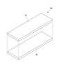
- 1 is an exploded perspective view showing the configuration of a laminated glass 10
- FIG. 3 is a plan view showing the arrangement of the light control cell 20 and the covering member 50.
- FIG. 3 is an exploded perspective view showing the configuration of a covering member 50
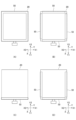
- FIG. (A) to (D) are plan views showing various forms of the covering member 50 provided in the light control cell 20.
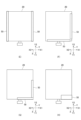
- FIG. (E) to (H) are plan views showing various forms of the covering member 50 provided in the light control cell 20.
- FIG. (A) to (E) are diagrams for explaining the manufacturing process of the laminated glass 10 having the light control cell 20 of the first embodiment. It is sectional drawing of 1 A of light modulation apparatuses which concern on 2nd Embodiment.
- FIG. 1 (described later), which serves as a reference for this coordinate system, is a diagram of the laminated glass 10 viewed from a direction (normal direction) perpendicular to the plate surface.
- the X-axis and Y-axis shown in FIG. 1 are axes parallel to the plate surface of the laminated glass 10, respectively.
- the laminated glass 10 shown in this embodiment has a rectangular shape, and a line parallel to one side thereof is the X-axis.
- One of the X directions along the X axis is defined as the X1 direction, and the direction opposite to the X1 direction is defined as the X2 direction.
- a line parallel to the side perpendicular to the X axis is the Y axis.
- one direction is the Y1 direction
- the opposite direction to the Y1 direction is the Y2 direction.
- the line perpendicular to the XY axis is the Z axis.
- One of the Z directions along the Z axis is the Z1 direction
- the opposite direction to the Z1 direction is the Z2 direction.
- direction is also referred to as "side”. Note that the numerical values, shapes, materials, and the like described in this specification are examples of embodiments, and are not limited to these, and may be appropriately selected and used.
- the light control device of each embodiment described below can be applied to various technical fields where control of light transmittance is required, and the scope of application is not particularly limited.
- the dimmer is intended for light control of, for example, window glass of buildings, showcases, indoor transparent partitions, vehicle windows (for example, front, side, rear, roof windows, etc.), partition boards inside vehicles, etc. Can be installed in parts. This makes it possible to control the amount of light incident on the inside of a building, vehicle, or the like, or to control the amount of light incident on a predetermined area inside the building, vehicle, or the like.
- the light control device of each embodiment may be configured with a three-dimensional shape having a curved surface shape.
- the light control device may have a shape that is convex on one side.
- the light modulation device is not limited to this, and the surface shape may be a planar shape (for example, flat plate shape), for example.
- the surface shape of the light control device is a planar shape (two-dimensional shape).
- FIG. 1 is a plan view of a light control device 1 according to the first embodiment.
- FIG. 2 is a cross-sectional view showing the s1-s1 cross section of FIG.
- FIG. 3 is an exploded perspective view showing the configuration of the laminated glass 10.
- FIG. 4 is a plan view showing the arrangement of the light control cell 20 and the covering member 50.
- FIG. 5 is an exploded perspective view showing the structure of the covering member 50. As shown in FIG.
- the light control device 1 of the first embodiment includes a laminated glass 10 and a frame member 11.
- the light control device 1 is a liquid crystal device in the present embodiment and the second embodiment, and is, for example, a device capable of controlling light transmittance by applying a voltage.
- the frame member 11 is a member that covers the outer peripheral portion of the laminated glass 10 in a frame shape.
- the frame member 11 is provided with an opening 11a. As shown in FIG. 2, the openings 11a are provided on both the front side (Z1 side) and the back side (Z2 side) of the light control device 1. As shown in FIG.
- the frame member 11 has a function of protecting the outer peripheral portion of the laminated glass 10 and a function of enabling the laminated glass 10 to be attached to a portion for adjusting light.
- the frame member 11 functions as a window frame.
- the frame member 11 is not limited to a shape that covers the outer peripheral portion of the laminated glass 10 in a frame shape, and may have a shape that partially covers the laminated glass 10 . Further, in the light control device, a configuration in which the frame member is not provided on the laminated glass may be adopted.
- the laminated glass 10 is a laminate including a light control cell 20 (described later) capable of controlling light transmittance by applying a voltage. As shown in FIGS. 2 and 3, the laminated glass 10 includes a first glass plate (first transparent substrate) 41, a second glass plate (second transparent substrate) 42, a first intermediate layer 31, and a second intermediate layer 32. , a dimming cell 20 and a covering member 50 . 1, illustration of the covering member 50 is omitted.
- the first glass plate 41 and the second glass plate 42 are members arranged facing each other on the front and back surfaces of the laminated glass 10 .
- the first glass plate 41 is arranged on the front side (Z1 side) of the laminated glass 10
- the second glass plate 42 is arranged on the back side (Z2 side) of the laminated glass 10 .
- plate glass with high translucency such as soda lime glass (blue plate glass), borosilicate glass (white plate glass), quartz glass, soda glass, potash glass, etc. may be used. can be done.
- resin glass can be used as the first glass plate 41 and the second glass plate 42 .
- the resin glass for example, one made of polycarbonate, acryl, or the like can be used.
- polycarbonate is preferable in terms of heat resistance and strength.
- the glass plate may be subjected to surface treatment such as hard coating, depending on required properties such as scratch resistance.
- resin glass is preferable to inorganic glass in terms of weight reduction.
- inorganic glass is preferable to resin glass in terms of cost, heat resistance, scratch resistance, and the like.
- the first intermediate layer 31 is provided between the first glass plate 41 and the light control cell 20, and is a layer that joins the first glass plate 41 and the light control cell 20 to each other.
- the first intermediate layer 31 is made of OCR (Optical Clear Resin).
- OCR is a cured product obtained by curing a liquid curable adhesive layer composition containing a polymerizable compound. Specifically, OCR applies a liquid resin obtained by mixing a base resin such as an acrylic resin, a silicone resin, or a urethane resin and an additive to an object, and then uses, for example, ultraviolet rays (UV). It is hardened.
- the first intermediate layer 31 made of OCR preferably has optical transparency, heat resistance up to at least about 120° C., moist heat resistance, and weather resistance.
- the second intermediate layer 32 is provided between the second glass plate 42 and the light control cell 20, and is a layer that joins the second glass plate 42 and the light control cell 20 to each other.
- the second intermediate layer 32 is made of OCA (Optical Clear Adhesive).
- the OCA is, for example, a layer made as follows. First, a release film such as polyethylene terephthalate (PET) is coated with a liquid curable adhesive layer composition containing a polymerizable compound, which is then cured using, for example, ultraviolet rays (UV) to form an OCA sheet.
- the curable adhesive layer composition may be an optical pressure-sensitive adhesive such as an acrylic resin, a silicone resin, or a urethane resin.
- the second intermediate layer 32 made of OCA preferably has optical transparency, heat resistance up to at least about 120° C., moist heat resistance, and weather resistance.
- the light control cell 20 is a liquid crystal cell in this embodiment, and is, for example, a film whose light transmittance can be controlled by voltage application.
- the light control cell 20 is sandwiched between the first glass plate 41 and the second glass plate 42 with intermediate layers (31, 32) interposed therebetween.
- the light control cell 20 includes a guest-host type liquid crystal composition using a dichroic dye as a liquid crystal layer 23 (described later).
- the dimming cell 20 comprises a first laminate 21, a second laminate 22, and a liquid crystal layer 23 disposed between the first laminate 21 and the second laminate 22. .
- the thickness of the dimming cell 20 is, for example, about 200 to 1000 ⁇ m.
- the light control cell 20 includes an active area A1 whose light transmittance is controlled and a non-active area A2 adjacent to the active area A1.
- the non-active area A2 is an area that is not used for light transmittance control.
- the area overlapping the frame member 11 in the normal direction (Z direction) of the light control cell 20 is the non-active area A2.
- an area that does not overlap with the frame member 11 in the normal direction (Z direction) of the light control cell 20 in other words, an area that overlaps with the opening 11a of the frame member 11 is the active area A1.
- non-active area A2 of the present embodiment is an area that does not have the function of controlling the transmittance of light or has the function of controlling the transmittance of the light in the outer peripheral portion adjacent to the active area A1 of the light control cell 20. Although provided, it corresponds to an area that is not used as the active area A1 in terms of design.
- the first laminate 21 includes a first substrate 24A, a first transparent electrode 25A and a first alignment layer 26A.
- the above parts are laminated in order of the first substrate 24A, the first transparent electrode 25A, and the first orientation layer 26A from the front side (Z1 side) to the back side (Z2 side).
- the second laminate 22 also includes a second substrate 24B, a second transparent electrode 25B and a second alignment layer 26B.
- the above parts are laminated in order of the second substrate 24B, the second transparent electrode 25B, and the second orientation layer 26B from the back side (Z2 side) to the front side (Z1 side).
- a plurality of bead spacers 27 are arranged between the first laminate 21 and the second laminate 22 .
- the liquid crystal layer 23 is formed by filling liquid crystal between the plurality of bead spacers 27 between the first laminate 21 and the second laminate 22 .
- the plurality of bead spacers 27 may be arranged irregularly or may be arranged regularly.
- the dimming cell 20 changes the voltage applied to the first transparent electrode 25A and the second transparent electrode 25B provided on the first laminate 21 and the second laminate 22, respectively, so that the guest-host liquid crystal of the liquid crystal layer 23 is changed.
- the composition changes the orientation of the liquid crystal material, thereby controlling the light transmittance.
- the first base material 24A and the second base material 24B are made of transparent resin, and flexible films can be applied.
- a transparent resin film having a small optical anisotropy and a transmittance of 80% or more in the visible wavelength range (380 nm or more and 800 nm or less).
- Materials for the transparent resin film include, for example, acetylcellulose-based resins such as triacetylcellulose (TAC), polyester-based resins such as polyethylene terephthalate (PET) and polyethylene naphthalate (PEN), polyethylene (PE), and polypropylene (PP).
- polystyrene, polymethylpentene, EVA and other polyolefin resins polyvinyl chloride, polyvinylidene chloride and other vinyl resins, acrylic resins, polyurethane resins, polysulfone (PSF), polyethersulfone (PES), polycarbonate ( PC), polyether, polyetherketone (PEK), (meth)acrylonitrile, cycloolefin polymer (COP), cycloolefin copolymer and the like.
- the transparent resin film As a material for the transparent resin film, resins such as polycarbonate, cycloolefin polymer, and polyethylene terephthalate are particularly preferable. Also, the thickness of the transparent resin film used as the first base material 24A and the second base material 24B can be appropriately selected within a range in which the transparent resin film has flexibility, although it depends on the material. The thickness of each of the first base material 24A and the second base material 24B may be 50 ⁇ m or more and 200 ⁇ m or less. In this embodiment, a polyethylene terephthalate film having a thickness of 125 ⁇ m is applied as an example of the first base material 24A and the second base material 24B.
- the first transparent electrode 25A and the second transparent electrode 25B are composed of transparent conductive films laminated on the first substrate 24A and the second substrate 24B (transparent resin film), respectively.
- transparent resin film various transparent electrode materials that are applied to this type of transparent resin film can be applied, and an oxide-based transparent metal thin film having a total light transmittance of 50% or more can be used. . Examples include tin oxide, indium oxide, and zinc oxide.
- Tin oxide (SnO 2 )-based materials include Nesa (tin oxide SnO 2 ), ATO (Antimony Tin Oxide), and FTO (fluorine-doped tin oxide).
- Indium oxide (In 2 O 3 )-based materials include indium oxide, ITO (Indium Tin Oxide), and IZO (Indium Zinc Oxide).
- Zinc oxide (ZnO)-based materials include zinc oxide, AZO (aluminum-doped zinc oxide), and GZO (gallium-doped zinc oxide).
- the transparent conductive film forming the first transparent electrode 25A and the second transparent electrode 25B is made of ITO.
- the bead spacer 27 is a member that defines the thickness (cell gap) of the liquid crystal layer 23 .
- spherical bead spacers are used as the bead spacers 27 .
- the diameter of the bead spacer 27 may range from 1 ⁇ m to 20 ⁇ m, preferably from 3 ⁇ m to 15 ⁇ m.
- the bead spacers 27 can be widely applied with inorganic materials such as silica, organic materials, core-shell structures combining these materials, and the like.
- the bead spacer 27 may be configured in a rod shape such as a cylindrical shape, an elliptical columnar shape, a polygonal columnar shape, or the like, in addition to the spherical configuration.
- the bead spacers 27 are made of a transparent member, but if necessary, a colored material may be applied to adjust the color.
- the bead spacers 27 are provided on the second laminate 22, but are not limited to this. may be provided only in Also, the bead spacers 27 may not necessarily be provided. Also, columnar spacers may be used instead of the bead spacers 27 or together with the bead spacers 27 .
- the first alignment layer 26A and the second alignment layer 26B are members for orienting the liquid crystal molecule group contained in the liquid crystal layer 23 in a desired direction.
- the first alignment layer 26A and the second alignment layer 26B are formed by photo-alignment layers.
- a photo-alignment material that can be applied to the photo-alignment layer various materials to which a photo-alignment technique can be applied can be widely applied. For example, photodegradation type, photodimerization type, photoisomerization type and the like can be mentioned. In a first embodiment, a photodimerization type material is used.
- photodimerizable materials include cinnamate, coumarin, benzylidenephthalimidine, benzylideneacetophenone, diphenylacetylene, stilbazole, uracil, quinolinone, maleimide, and polymers having cinnamylideneacetic acid derivatives.
- a polymer containing either or both of cinnamate and coumarin is preferably used because of its good orientation control force.
- a rubbing alignment layer may be used instead of the photo-alignment layer.
- the rubbing treatment may not be performed, or the alignment layer may be produced by performing a rubbing treatment and performing a molding treatment to form a fine line-shaped concave-convex shape.
- the light control cell 20 includes the first alignment layer 26A and the second alignment layer 26B, but is not limited to this. may be
- a guest-host liquid crystal composition and a dichroic dye composition can be widely applied to the liquid crystal layer 23 .
- the guest-host liquid crystal composition may contain a chiral agent so that when the liquid crystal material is horizontally aligned, it is aligned in a spiral shape in the thickness direction of the liquid crystal layer 23 .
- a ring-shaped or frame-shaped sealing material 28 is arranged in plan view so as to surround the liquid crystal layer 23 .
- the sealing material 28 holds the first layered body 21 and the second layered body 22 together and prevents leakage of the liquid crystal material.
- Thermosetting resins such as epoxy resins and acrylic resins, ultraviolet curable resins, and the like can be applied to the sealing material 28 .
- a nematic liquid crystal compound, a smectic liquid crystal compound, and a cholesteric liquid crystal compound can be applied to the liquid crystal layer 23 as liquid crystal compounds having no polymerizable functional group.
- nematic liquid crystal compounds include biphenyl-based compounds, terphenyl-based compounds, phenylcyclohexyl-based compounds, biphenylcyclohexyl-based compounds, phenylbicyclohexyl-based compounds, trifluoro-based compounds, phenyl benzoate-based compounds, and phenyl cyclohexylbenzoate-based compounds.
- phenyl phenylbenzoate compounds phenyl bicyclohexylcarboxylate compounds, azomethine compounds, azo compounds, and azooxy compounds, stilbene compounds, tolan compounds, ester compounds, bicyclohexyl compounds, phenylpyrimidine compounds , biphenylpyrimidine-based compounds, pyrimidine-based compounds, and biphenylethyne-based compounds.
- smectic liquid crystal compounds include ferroelectric polymer liquid crystal compounds such as polyacrylate, polymethacrylate, polychloroacrylate, polyoxirane, polysiloxane, and polyester.
- cholesteric liquid crystal compounds include cholesteryl linoleate, cholesteryl oleate, cellulose, cellulose derivatives, and polypeptides.
- Dichroic dyes used in the guest-host system include liquid crystal-soluble and highly dichroic dyes such as azo, anthraquinone, quinophthalone, perylene, indigo, thioindigo, and merocyanine dyes. dichroic dyes such as dyes, styryl dyes, azomethine dyes, and tetrazine dyes.
- the alignment control force related to pretilt is set in a certain direction for the first alignment layer 26A and the second alignment layer 26B so that the alignment of the guest-host liquid crystal composition is formed when there is no electric field when the light is blocked. It consists of horizontal alignment layers, which are normally dark. It should be noted that the light control cell 20 may be set to normally clear when the electric field is applied when the light is shielded. Here, normally dark means a structure in which light transmittance is minimized when no voltage is applied to the liquid crystal, resulting in a black screen. Normally clear is a structure in which light transmittance is maximized and the liquid crystal becomes transparent when no voltage is applied.
- the haze value of the light-transmitting light control cell 20 is desirably 30% or less, and more desirably 15% or less. In order to achieve such a low haze value, it is desirable that the liquid crystal mixture contains no polymerizable compound.
- the light control cell 20 may be configured to include a liquid crystal layer 23 such as a TN (Twisted Nematic) method, a VA (Vertical Alignment) method, or an IPS (In-Plane-Switching) method that does not use a dichroic dye composition.
- a liquid crystal layer 23 such as a TN (Twisted Nematic) method, a VA (Vertical Alignment) method, or an IPS (In-Plane-Switching) method that does not use a dichroic dye composition.
- a liquid crystal layer 23 such as a TN (Twisted Nematic) method, a VA (Vertical Alignment) method, or an IPS (In-Plane-Switching) method that does not use a dichroic dye composition.
- a flexible printed wiring board 29 (see FIG. 3) is provided for electrical connection between the first transparent electrode 25A and the second transparent electrode 25B and the outside.
- the flexible printed wiring board 29 is connected by being sandwiched between the first transparent electrode 25A and the second transparent electrode 25B in a region where the liquid crystal layer 23 is not sandwiched between the first transparent electrode 25A and the second transparent electrode 25B.
- the flexible printed wiring board 29 may have a form in which it is not sandwiched between the first transparent electrode 25A and the second transparent electrode 25B, for example.
- the covering member 50 is a member for adjusting the thickness of the first intermediate layer 31 interposed between the outer peripheral portion of the light control cell 20 and the first glass plate 41 .
- the peripheral portion of the dimming cell 20 refers to the non-active area A2 or a region including part of the non-active area A2.
- the covering member 50 of the first embodiment is arranged on the surface (Z1 side) of the light control cell 20 .
- the covering member 50 is formed in an elongated rectangular shape. In this embodiment, two covering members 50 are provided on each side of the light control cell 20 . Between the adjacent covering members 50, gaps (clearances) S are provided as shown in FIG.
- the light control cell 20 has a region that overlaps with the covering member 50 and a region that does not overlap with the covering member 50 .
- the covering member 50 may not be provided as shown in FIG. 4, and may be continuous along one side of the light control cell 20 as described later. 4, the outer edge of the covering member 50 protrudes outside the outer peripheral edge 20a of the light control cell 20, but is arranged so that the outer edge coincides with the outer peripheral edge 20a of the light control cell 20. may have been
- the covering member 50 includes a film material 51 and a bonding layer 52, as shown in FIG.
- the film material 51 is a member arranged on the first glass plate 41 side in the covering member 50 .
- the film material 51 for example, in addition to polyethylene terephthalate (PET), the same material as the above-described first base material 24A and second base material 24B can be used.
- PET polyethylene terephthalate
- the covering member 50 may be transparent or opaque. However, since the following effects can be obtained by making the covering member 50 transparent, it is more desirable to make the covering member 50 transparent. As for the effect of making the covering member 50 transparent, it is possible to minimize the possibility of overlooking the problem with the surrounding area of the light-modulating cell during the manufacturing process, if the covering member 50 is transparent. It can be made smaller.
- the degree of transparency of the covering member 50 is desirably 50% or more, and more desirably 80% or more.
- the above transmittance is a value in the visible light region (400 nm to 800 nm) and is measured with a spectrophotometer.
- the thickness of the covering member 50 is preferably 25% or more and 95% or less, more preferably 40% or more and 90% or less, of the thickness of the first intermediate layer 31 .
- the thickness of the film material 51 is desirably, for example, 50 to 250 ⁇ m, more desirably 100 to 250 ⁇ m.
- the bonding layer 52 is a layer that bonds the film material 51 and the light control cell 20 .
- the bonding layer 52 is arranged on the side of the light control cell 20 in the covering member 50 .
- OCA, OCR, or the like can be used as the bonding layer 52 .
- the thickness of the bonding layer 52 is, for example, 15 to 250 ⁇ m.
- the covering member 50 may have a configuration in which the bonding layer 52 is omitted. As shown in FIG. 2, the covering member 50 is provided in a region that does not overlap the active area A1 of the light control cell 20 in plan view.
- the covering member 50 of the present embodiment is provided so as to cover almost the entire non-active area A2 of the light control cell 20 except for the gap S. In addition, when the covering member 50 is provided in one place, it may be applied to the area of the covering member 50 in that one place.
- FIG. 6A to 6D and 7E to 7H are plan views showing various forms of the covering member 50 provided on the light control cell 20.
- FIG. FIG. 6A shows a form in which a frame-shaped covering member 50 is provided on the outer peripheral portion of the light control cell 20 .
- FIG. 6B shows a form in which a covering member 50 is provided so as to cover the four sides of the light control cell 20.
- FIG. FIG. 6(C) shows a form in which a covering member 50 is provided so as to cover one side of the light control cell 20 .
- FIG. 6C shows a mode in which the covering member 50 is provided on one side of the light control cell 20 on the Y1 side. may be FIG.
- FIG. 6D shows a form in which a covering member 50 is provided so as to cover three sides of the light control cell 20.
- FIG. FIG. 6D shows a mode in which the covering member 50 is provided on three sides of the light control cell 20 except for the Y2 side. It is good also as a form provided in.
- FIG. 7(E) shows a form in which the covering member 50 is provided so as to cover the two opposing sides of the light control cell 20 .
- FIG. 7(E) shows a mode in which the covering member 50 is provided on two sides of the light control cell 20 on the X1 side and the X2 side. It is good also as a form provided in the side.
- FIG. 7(F) shows a form in which a covering member 50 is provided so as to cover two adjacent sides of the light control cell 20 .
- FIG. 7F shows a mode in which the covering member 50 is provided on two sides of the light control cell 20, namely, the X1 side and the Y1 side. can be placed in any position.
- the covering member 50 may be provided on two sides of the dimming cell 20, namely, the X2 side and the Y2 side.
- FIG. 7(G) shows a form in which a covering member 50 having a length shorter than one side of the light control cell 20 is provided on two adjacent sides of the light control cell 20 .
- FIG. 7G shows a mode in which the covering member 50 is provided on two sides of the light control cell 20, namely, the X1 side and the Y1 side. can be placed in any position.
- the covering member 50 may be provided on two sides of the dimming cell 20, namely, the X2 side and the Y2 side.
- the length of the covering member 50 provided at each position may be different from that shown in FIG. 7(G).
- FIG. 7(H) shows a form in which a covering member 50 having a shorter length in the X direction than one side of the light control cell 20 and a wider width in the Y direction is provided on one side of the light control cell 20.
- FIG. 7(H) shows a form in which the covering member 50 is provided on the Y1 side and the X1 side of the light control cell 20.
- the covering member 50 is provided on one side of the light control cell 20, It may be provided at any position as long as it is shorter and wider than one side.
- the light control cell 20 when the light control cell 20 (light control device 1) is placed vertically, for example, when the Y direction of the light control cell 20 is the vertical direction and the Y2 side is the upper side, the light control cell In 20, liquid crystal accumulation is likely to occur on the lower side (Y1 side) of the active area A1. Therefore, when the light control cell 20 is placed vertically in the above direction, by arranging the covering member 50 on the lower side (Y1 side) of the light control cell 20, the liquid crystal pool generated on the Y1 side of the active area A1 is reduced. can be made inconspicuous. When the light control cell 20 is placed vertically in the above direction, it is preferable to arrange the covering member 50 as shown in FIGS. form.
- FIG. 8A to 8E are diagrams for explaining the manufacturing process of the laminated glass 10 having the light control cell 20 of the first embodiment.
- the second glass plate 42 is placed on a workbench (not shown), and the second intermediate layer 32 made of OCA is formed on the second glass plate 42. Laminate.
- the light control cell 20 is laminated on the second intermediate layer 32 .
- the covering member 50 is arranged around the outer periphery of the light control cell 20 (for example, the form shown in FIG. 3). The covering member 50 is laminated so that the bonding layer 52 is on the side of the light control cell 20 and the film material 51 is on the side opposite to the light control cell 20 .
- uncured OCR which will be the first intermediate layer 31, is applied on the laminate obtained in FIG. 8(C). OCR is applied by, for example, a dispenser, slit coater, or other application nozzle (not shown).
- the first glass plate 41 is bonded onto the first intermediate layer 31.
- the first intermediate layer 31 is an OCR containing a non-pressure-bonding adhesive component
- the first glass plate 41 can be bonded by atmospheric bonding or vacuum bonding without applying pressure.
- the OCR can be cured by irradiating the laminate with ultraviolet rays (UV).
- UV ultraviolet rays
- the light control cell 20 of this embodiment has a region that overlaps with the covering member 50 and a region that does not overlap with the covering member 50 . Therefore, in the laminated glass 10 sandwiching the light control cell 20, the thickness of the first intermediate layer 31 in the region where the covering member 50 is arranged is thinner than the region where the covering member 50 is not arranged.
- the OCR that contacts the light control cell 20 in the region that does not overlap with the covering member 50 expands more than the OCR that contacts the light control cell 20 in the region that overlaps with the covering member 50 . Due to the expansion, the OCR contacting the light control cell 20 in the region not overlapping the covering member 50 presses the light control cell 20 more strongly than the OCR contacting the light control cell 20 in the region overlapping the covering member 50 . As a result, part of the liquid crystal present in the region that does not overlap with the covering member 50 moves to the region that overlaps with the covering member 50, that is, the region where OCR expansion is small.
- the covering member 50 in a region where the liquid crystal is to be moved in the light control cell 20, part of the liquid crystal filled in the cell can be selectively collected in that region.
- the region where liquid crystal pooling occurs can be controlled. Therefore, in the light control cell 20, by arranging the covering member 50 in a region adjacent to a region in which liquid crystal pooling is not desired, it is possible to suppress appearance defects of the light control cell 20 in that region.
- the light control cell 20 has the covering member 50 arranged along the outer peripheral portion as shown in FIG.
- the thickness of layer 31 becomes thinner than other areas (eg, active area A1). Therefore, when the OCR that forms the first intermediate layer 31 is cured during the production of the laminated glass 10, the expansion of the OCR in the outer peripheral portion of the light control cell 20 is relatively greater than the expansion of the OCR in the central portion. become smaller. Accordingly, when the OCR is cured, the OCR in contact with the central portion of the light control cell 20 expands more than the outer peripheral portion and presses the central portion of the light control cell 20 more strongly.
- part of the liquid crystal present in the central portion of the light control cell 20 moves to the outer peripheral portion where the expansion of the OCR is small. That is, part of the liquid crystal present in the central portion of the light control cell 20 (laminated glass 10) is collected in the non-active area A2 where the covering member 50 is arranged during manufacture.
- the manufactured light control cell 20 laminated glass 10
- the liquid crystal pools in the central portion of the light control cell 20. Since it is less likely to occur, it is possible to suppress appearance defects and deterioration of dimming performance mainly in the active area A1.
- the covering member 50 is provided on the light control cell 20 side. Therefore, in the step shown in FIG. 8(C), the work of arranging the covering member 50 on the outer peripheral portion of the light control cell 20 can be easily performed.
- the covering member 50 is composed of a film material 51 and a bonding layer 52 (see FIG. 5). Therefore, in the step shown in FIG. 8D, when the OCR is applied onto the light control cell 20, the position of the covering member 50 arranged on the outer peripheral portion of the light control cell 20 can be made less likely to shift.
- the covering member 50 is provided at two positions on each side of the light control cell 20, and the gap S is provided between the adjacent covering members 50. is provided. Therefore, in the process shown in FIG. 8(E), when the uncured OCR is sandwiched between the first glass plate 41 and the light control cell 20 to form the first intermediate layer 31, excess air is removed from the gap S. can be discharged.
- a light modulation device 1A of the second embodiment differs from that of the first embodiment in the position where the covering member 50 is arranged.
- 1 A of light modulation apparatuses of 2nd Embodiment other structures are the same as that of 1st Embodiment. Therefore, in description of 2nd Embodiment, only sectional drawing of 1 A of light control apparatuses is illustrated, and other figures are abbreviate
- the same reference numerals as in the first embodiment are given to members and the like that are the same as those in the first embodiment, and overlapping descriptions are omitted.
- FIG. 9 is a cross-sectional view of a light control device 1A according to the second embodiment.
- FIG. 9 corresponds to a cross-sectional view (FIG. 2) of the light control device 1 of the first embodiment.
- the covering member 50 is arranged on the surface of the first glass plate 41 (Z2 side).
- the film material 51 (see FIG. 5) is arranged on the light control cell 20 side.
- the bonding layer 52 (see FIG. 5) is arranged on the first glass plate 41 side.
- the area where the covering member 50 is arranged is the same as in the first embodiment.
- the covering member 50 is provided in a region that does not overlap the active area A1 of the light control cell 20 in plan view.
- the arrangement of the covering member 50 is, for example, the forms of FIGS. 4, 6 (A) to (D) and 7 (E) to (H) of the first embodiment. can be applied.
- the coating member 50 arranged along the outer peripheral portion of the light control cell 20 prevents part of the liquid crystal present in the center of the light control cell 20 from being They can be collected within the area of the active area A2. Therefore, according to the light control device 1A of the second embodiment, when the light control cell 20 (laminated glass 10) is exposed to a high temperature environment, the deterioration of the appearance and the light control performance in the active area A1 can be prevented. can be suppressed.
- the covering member 50 has an elongated rectangular shape
- the shape of the covering member 50 may be, for example, a square, a rectangle, a parallelogram, a trapezoid, a circle, an ellipse, or the like in plan view. That is, the shape of the covering member 50 in plan view can be changed as appropriate.
- the dimming cell 20 is rectangular in plan view, but it is not limited to this.
- the shape of the dimming cell 20 may be, for example, a square in plan view, a parallelogram, a trapezoid, or the like. That is, the shape of the light control cell 20 in plan view can be changed as appropriate.
- the configuration in which the covering member 50 is provided on the light control cell 20 side (first embodiment) and the configuration in which the covering member 50 is provided on the first glass plate 41 side (second embodiment) have been described, but are limited to this. not.
- the first intermediate layer 31 (OCR) may be sandwiched between the covering members 50 on the light control cell 20 side and the first glass plate 41 side.
- the covering member 50 provided on the light control cell 20 side and the covering member 50 provided on the first glass plate 41 side may have the same shape or arrangement, or may be different.
- the present invention is not limited to this.
- a functional film such as a UV cut film may be laminated on one side or both sides of the light control cell 20 .
- the example in which the first intermediate layer 31 of the laminated glass 10 is made of OCR and the second intermediate layer 32 is made of OCA has been described, but the present invention is not limited to this.
- Each of the first intermediate layer 31 and the second intermediate layer 32 may be configured by OCR.
- Reference Signs List 1 1A light control device 10 laminated glass 11 frame member 20 light control cell 31 first intermediate layer 32 second intermediate layer 41 first glass plate 42 second glass plate 50 covering member 51 film material 52 bonding layer S gap A1 active Area A2 Inactive area
Landscapes
- Physics & Mathematics (AREA)
- Nonlinear Science (AREA)
- Chemical & Material Sciences (AREA)
- Crystallography & Structural Chemistry (AREA)
- General Physics & Mathematics (AREA)
- Optics & Photonics (AREA)
- Mathematical Physics (AREA)
- Liquid Crystal (AREA)
Abstract
液晶セルの外観不良を抑制することができる合わせガラスを提供する。 合わせガラス10は、第1透明基板41と、第1透明基板41と対向して配置される第2透明基板42と、前記第1透明基板と前記第2透明基板との間に設けられる液晶セル20と、第1透明基板41と液晶セル20との間に設けられる、OCRからなる第1中間層31と、第2透明基板42と液晶セル20との間に設けられる、OCAからなる第2中間層32と、液晶セル20と第1透明基板41との間に設けられる被覆部材50と、を備え、調光セル20は、被覆部材50と重なる領域と、被覆部材50と重ならない領域とを有する。
Description
本発明は、合わせガラス及びこれを備えた液晶装置に関する。
従来、窓等に用いられ、光の透過率を制御する電子ブラインドに利用可能な調光部材、この調光部材を用いた調光装置が提案されている。例えば、調光部材として液晶セル(調光セル)を用い、この液晶セルを一対のガラスで挟み込んで合わせガラスとすることが提案されている(例えば、特許文献1,2参照)。
液晶セルを挟み込んだ合わせガラスを高温の環境下に晒した場合、液晶セルの基材や液晶層が膨張する。その結果、液晶セルに封入された液晶が局所的に偏在する現象(以下、「液晶溜まり」ともいう)が不規則な形状で発生する。この液晶溜まりは、外観不良と認識される場合があるため、これを抑制することが望まれている。
本発明の目的は、液晶セルの外観不良を抑制することができる合わせガラス及び液晶装置を提供することにある。
本発明は、以下のような解決手段により、課題を解決する。なお、理解を容易にするために、本発明の実施形態に対応する符号を付して説明するが、これに限定されるものではない。また、符号を付して説明した構成は、適宜に改良してもよく、また、少なくとも一部を他の構成物に代替してもよい。本開示の実施形態は、以下の[1]~[10]に関する。
[1] 第1の発明は、第1透明基板(41)と、前記第1透明基板と対向して配置される第2透明基板(42)と、前記第1透明基板と前記第2透明基板との間に設けられる液晶セル(20)と、前記第1透明基板と前記液晶セルとの間に設けられる、OCRからなる第1中間層(31)と、前記第2透明基板と前記液晶セルとの間に設けられる、OCAからなる第2中間層(32)と、前記液晶セルと前記第1透明基板との間に設けられる被覆部材(50)と、を備え、前記液晶セルは、平面視において、前記被覆部材と重なる領域と、前記被覆部材と重ならない領域と、を有する合わせガラス(10)。
[2] 第2の発明は、第1透明基板(41)と、前記第1透明基板と対向して配置される第2透明基板(42)と、前記第1透明基板と前記第2透明基板との間に設けられ、光の透過率が制御されるアクティブエリア(A1)及び光の透過率の制御に用いられない非アクティブエリア(A2)を有する液晶セル(20)と、前記第1透明基板と前記液晶セルとの間に設けられる第1中間層(31)と、前記第2透明基板と前記液晶セルとの間に設けられる第2中間層(32)と、前記液晶セルと前記第1透明基板との間に設けられる被覆部材(50)と、を備え、前記被覆部材は、平面視において、前記液晶セルの前記アクティブエリアと重複しない合わせガラス(10)。
[3] [2]に記載の合わせガラスにおいて、前記第1中間層は、OCRであり、前記第2中間層は、OCAであってもよい。
[4] [1]から[3]までのいずれかに記載の合わせガラスにおいて、前記被覆部材がフィルム材(51)と接合層(52)により構成されていてもよい。
[5] [1]から[4]までのいずれかに記載の合わせガラスにおいて、前記被覆部材が前記液晶セルの前記第1透明基板側の表面上に設けられていてもよい。
[6] [1]から[4]までのいずれかに記載の合わせガラスにおいて、前記被覆部材が前記第1透明基板の前記液晶セル側の表面上に設けられていてもよい。
[7] [1]から[6]までのいずれかに記載の合わせガラスにおいて、前記被覆部材の厚みが前記第1中間層の厚みの25%以上75%以下であってもよい。
[8] [1]から[7]までのいずれかに記載の合わせガラスにおいて、隣接する前記被覆部材の間に隙間が設けられていてもよい。
[9] [1]から[8]までのいずれかに記載の合わせガラスにおいて、前記被覆部材は、透明であってもよい。
[10] [1]から[9]までのいずれかに記載の合わせガラスと、前記合わせガラスの外周部を保持する枠部材(11)と、を備える液晶装置(1)。
本発明に係る合わせガラス及び液晶装置によれば、液晶セルの外観不良を抑制することができる。
以下、本発明の実施形態について説明する。なお、本明細書に添付した図面は、いずれも模式図であり、理解しやすさ等を考慮して、各部の形状、縮尺、縦横の寸法比等を、実物から変更又は誇張している。また、図面においては、部材の断面を示すハッチングを適宜に省略する。
本明細書等において、形状、幾何学的条件、これらの程度を特定する用語、例えば、「平行」、「直交」、「方向」等の用語については、その用語の厳密な意味に加えて、ほぼ平行、ほぼ直交等とみなせる程度の範囲、概ねその方向とみなせる範囲を含む。
本明細書等においては、板、シート、フィルム等の用語を使用しているが、これら部材は、一般的な厚さの区分に限定されず、適宜に置き換え可能とする。例えば、「OCAシート」は、「OCAフィルム」と置き換えてもよい。
本明細書等においては、板、シート、フィルム等の用語を使用しているが、これら部材は、一般的な厚さの区分に限定されず、適宜に置き換え可能とする。例えば、「OCAシート」は、「OCAフィルム」と置き換えてもよい。
また、図面には、必要に応じてX-Y-Zの互いに直交する座標系を記載した。この座標系の基準となる図1(後述)は、合わせガラス10を板面に対して垂直な方向(法線方向)から見た図である。図1に示すX軸、Y軸は、それぞれ合わせガラス10の板面に平行な軸である。本実施形態に示す合わせガラス10は、長方形であり、その一辺に平行な線がX軸である。このX軸に沿うX方向のうち、一方の方向をX1方向とし、このX1方向と反対の方向をX2方向とする。また、X軸と直交する辺に平行な線がY軸である。このY軸に沿うY方向のうち、一方の方向をY1方向とし、このY1方向と反対の方向をY2方向とする。更に、X-Y軸と直交する線がZ軸である。このZ軸に沿うZ方向のうち、一方の方向をZ1方向とし、このZ1方向と反対の方向をZ2方向とする。以下の説明においては、「~方向」を「~側」ともいう。
なお、本明細書中に記載する数値、形状、材料等は、実施形態としての一例であり、これに限定されるものではなく、適宜に選択して使用してもよい。
なお、本明細書中に記載する数値、形状、材料等は、実施形態としての一例であり、これに限定されるものではなく、適宜に選択して使用してもよい。
以下に説明する各実施形態の調光装置は、光の透過率の制御が求められる様々な技術分野に適用可能であり、その適用範囲は特に限定されない。調光装置は、例えば、建築物の窓ガラス、ショーケース、屋内の透明パーテーション、車両のウインドウ(例えば、フロント、サイド、リア、ルーフ等のウインドウ)、車両内部のパーテーションボード等の調光を図る部位に設置することができる。これにより、建築物や車両等の内側への入射光の光量を制御したり、建築物や車両等の内部における所定区域への入射光の光量を制御したりすることができる。
また、各実施形態の調光装置は、表面形状が曲面形状を有する3次元形状により構成されていてもよい。例えば、調光装置は、一方の面側に凸となる形状を有していてもよい。また、調光装置は、これに限らず、例えば、表面形状が平面形状(例えば、平板状)であってもよい。各実施形態では、調光装置の表面形状が平面形状(2次元形状)により構成されるものとして説明する。
(第1実施形態)
図1は、第1実施形態に係る調光装置1の平面図である。図2は、図1のs1-s1断面を示す断面図である。図3は、合わせガラス10の構成を示す分解斜視図である。図4は、調光セル20と被覆部材50の配置を示す平面図である。図5は、被覆部材50の構成を示す分解斜視図である。
図1は、第1実施形態に係る調光装置1の平面図である。図2は、図1のs1-s1断面を示す断面図である。図3は、合わせガラス10の構成を示す分解斜視図である。図4は、調光セル20と被覆部材50の配置を示す平面図である。図5は、被覆部材50の構成を示す分解斜視図である。
図1及び図2に示すように、第1実施形態の調光装置1は、合わせガラス10と、枠部材11と、を備えている。調光装置1は、本実施形態及び第2実施形態において液晶装置であり、例えば、電圧の印加により光透過率を制御可能な装置である。
枠部材11は、合わせガラス10の外周部を枠形に覆う部材である。枠部材11には、開口部11aが設けられている。図2に示すように、開口部11aは、調光装置1の表面側(Z1側)と裏面側(Z2側)の両方に設けられている。後述する調光セル20の法線方向(Z方向)において、開口部11aの位置、形状及び大きさは、調光セル20のアクティブエリアA1(後述)と一致している。枠部材11は、合わせガラス10の外周部を保護する機能と、合わせガラス10を、調光を図る部位に取り付け可能とする機能と、を備えている。例えば、合わせガラス10を建築物の窓ガラスに適用した場合、枠部材11は、窓枠として機能する。なお、枠部材11は、合わせガラス10の外周部を枠形に覆う形状に限らず、合わせガラス10を部分的に覆う形状であってもよい。また、調光装置において、合わせガラスに枠部材を設けない構成としてもよい。
枠部材11は、合わせガラス10の外周部を枠形に覆う部材である。枠部材11には、開口部11aが設けられている。図2に示すように、開口部11aは、調光装置1の表面側(Z1側)と裏面側(Z2側)の両方に設けられている。後述する調光セル20の法線方向(Z方向)において、開口部11aの位置、形状及び大きさは、調光セル20のアクティブエリアA1(後述)と一致している。枠部材11は、合わせガラス10の外周部を保護する機能と、合わせガラス10を、調光を図る部位に取り付け可能とする機能と、を備えている。例えば、合わせガラス10を建築物の窓ガラスに適用した場合、枠部材11は、窓枠として機能する。なお、枠部材11は、合わせガラス10の外周部を枠形に覆う形状に限らず、合わせガラス10を部分的に覆う形状であってもよい。また、調光装置において、合わせガラスに枠部材を設けない構成としてもよい。
(合わせガラス)
合わせガラス10は、電圧の印加により光の透過率を制御可能な調光セル20(後述)を含む積層体である。図2及び図3に示すように、合わせガラス10は、第1ガラス板(第1透明基板)41、第2ガラス板(第2透明基板)42、第1中間層31、第2中間層32、調光セル20及び被覆部材50を備えている。なお、図1では、被覆部材50の図示を省略している。
合わせガラス10は、電圧の印加により光の透過率を制御可能な調光セル20(後述)を含む積層体である。図2及び図3に示すように、合わせガラス10は、第1ガラス板(第1透明基板)41、第2ガラス板(第2透明基板)42、第1中間層31、第2中間層32、調光セル20及び被覆部材50を備えている。なお、図1では、被覆部材50の図示を省略している。
第1ガラス板41及び第2ガラス板42は、それぞれ合わせガラス10の表裏面に、対向して配置される部材である。例えば、第1ガラス板41が合わせガラス10の表面側(Z1側)に配置されるとすると、第2ガラス板42は、合わせガラス10の裏面側(Z2側)に配置される。第1ガラス板41及び第2ガラス板42としては、例えば、ソーダライムガラス(青板ガラス)、硼珪酸ガラス(白板ガラス)、石英ガラス、ソーダガラス、カリガラス等の透光性の高い板ガラスを用いることができる。
また、第1ガラス板41及び第2ガラス板42として、樹脂ガラスを用いることができる。樹脂ガラスとしては、例えば、ポリカーボネート、アクリル等からなるものを用いることができる。特に、ポリカーボネートは、耐熱性、強度の面で好ましい。更に、ガラス板には、耐擦傷性等の要求特性に応じて、ハードコート等の表面処理がなされてもよい。ガラス板の材料としては、無機ガラスより樹脂ガラスの方が軽量化の面で好ましい。他方、無機ガラスの方が樹脂ガラスよりコスト、耐熱性、耐傷性等の面で好ましい。
第1中間層31は、第1ガラス板41と調光セル20との間に設けられ、第1ガラス板41と調光セル20とを互いに接合させる層である。第1実施形態において、第1中間層31は、OCR(Optical Clear Resin)により構成されている。OCRは、重合性化合物を含む液状の硬化性接着層用組成物を硬化した硬化物である。具体的には、OCRは、アクリル系樹脂、シリコーン系樹脂又はウレタン系樹脂等のベース樹脂と添加剤とを混合した液状の樹脂を対象物に塗布した後、例えば紫外線(UV)等を用いて硬化したものである。OCRからなる第1中間層31は、光学透明性を有しており、更に少なくとも120℃程度までの耐熱性、耐湿熱性、耐候性を有することが好ましい。
第2中間層32は、第2ガラス板42と調光セル20との間に設けられ、第2ガラス板42と調光セル20とを互いに接合させる層である。第1実施形態において、第2中間層32は、OCA(Optical Clear Adhesive)により構成されている。OCAは、例えば、以下のようにして作製された層である。まず、ポリエチレンテレフタレート(PET)等の離型フィルム上に、重合性化合物を含む液状の硬化性接着層用組成物を塗布し、これを例えば紫外線(UV)等を用いて硬化させて、OCAシートを得る。上記硬化性接着層用組成物は、アクリル系樹脂、シリコーン系樹脂又はウレタン系樹脂等の光学用粘着剤であってもよい。このOCAシートを対象物に貼合した後、離型フィルムを剥離することにより、上記OCAからなる層が得られる。OCAからなる第2中間層32は、光学透明性を有しており、更に少なくとも120℃程度までの耐熱性、耐湿熱性、耐候性を有することが好ましい。
(調光セル)
調光セル20は、本実施形態において液晶セルであり、例えば、電圧の印加により光の透過率を制御可能なフィルムである。調光セル20は、第1ガラス板41と第2ガラス板42との間に中間層(31、32)を介して挟持されている。調光セル20は、液晶層23(後述)として、二色性色素を使用したゲストホスト型の液晶組成物を備えている。図2に示すように、調光セル20は、第1積層体21、第2積層体22及び第1積層体21と第2積層体22との間に配置された液晶層23を備えている。調光セル20の厚みは、例えば、200~1000μm程度である。
調光セル20は、本実施形態において液晶セルであり、例えば、電圧の印加により光の透過率を制御可能なフィルムである。調光セル20は、第1ガラス板41と第2ガラス板42との間に中間層(31、32)を介して挟持されている。調光セル20は、液晶層23(後述)として、二色性色素を使用したゲストホスト型の液晶組成物を備えている。図2に示すように、調光セル20は、第1積層体21、第2積層体22及び第1積層体21と第2積層体22との間に配置された液晶層23を備えている。調光セル20の厚みは、例えば、200~1000μm程度である。
図1及び図2に示すように、調光セル20は、光の透過率が制御されるアクティブエリアA1と、アクティブエリアA1に隣接する非アクティブエリアA2と、を備えている。非アクティブエリアA2は、光の透過率の制御に用いられない領域となる。本実施形態においては、図2に示すように、調光セル20の法線方向(Z方向)において、枠部材11と重なる領域が非アクティブエリアA2となる。一方、調光セル20の法線方向(Z方向)において、枠部材11と重ならない領域、言い換えると、枠部材11の開口部11aと重なる領域がアクティブエリアA1となる。なお、本実施形態の非アクティブエリアA2は、調光セル20のアクティブエリアA1に隣接する外周部において、光の透過率を制御する機能を備えていない領域又は光の透過率を制御する機能を備えているが、設計上、アクティブエリアA1として用いられない領域に相当する。
図2に示すように、調光セル20において、第1積層体21は、第1基材24A、第1透明電極25A及び第1配向層26Aを備えている。第1積層体21において、上記各部は、表面側(Z1側)から裏面側(Z2側)に向けて、第1基材24A、第1透明電極25A、第1配向層26Aの順に積層されている。また、第2積層体22は、第2基材24B、第2透明電極25B及び第2配向層26Bを備えている。第2積層体22において、上記各部は、裏面側(Z2側)から表面側(Z1側)に向けて、第2基材24B、第2透明電極25B及び第2配向層26Bの順に積層されている。
第1積層体21と第2積層体22との間には、複数のビーズスペーサー27が配置されている。液晶層23は、第1積層体21と第2積層体22との間において、複数のビーズスペーサー27の間に液晶が充填されることにより、形成されている。複数のビーズスペーサー27は、それぞれ不規則的に配置されていてもよいし、規則的に配置されていてもよい。
調光セル20は、第1積層体21及び第2積層体22にそれぞれ設けられた第1透明電極25A及び第2透明電極25Bに印加する電圧を変化させることにより、液晶層23のゲストホスト液晶組成物による液晶材料の配向が変化し、これにより光の透過率が制御される。
調光セル20は、第1積層体21及び第2積層体22にそれぞれ設けられた第1透明電極25A及び第2透明電極25Bに印加する電圧を変化させることにより、液晶層23のゲストホスト液晶組成物による液晶材料の配向が変化し、これにより光の透過率が制御される。
第1基材24A及び第2基材24Bは、透明な樹脂製であって、可撓性を有するフィルムを適用することができる。第1基材24A及び第2基材24Bとしては、光学異方性が小さく、可視域の波長(380nm以上800nm以下)における透過率が80%以上である透明樹脂フィルムを適用することが望ましい。透明樹脂フィルムの材料としては、例えば、トリアセチルセルロース(TAC)等のアセチルセルロース系樹脂、ポリエチレンテレフタレート(PET)、ポリエチレンナフタレート(PEN)等のポリエステル系樹脂、ポリエチレン(PE)、ポリプロピレン(PP)、ポリスチレン、ポリメチルペンテン、EVA等のポリオレフィン系樹脂、ポリ塩化ビニル、ポリ塩化ビニリデン等のビニル系樹脂、アクリル系樹脂、ポリウレタン系樹脂、ポリサルホン(PSF)、ポリエーテルサルホン(PES)、ポリカーボネート(PC)、ポリエーテル、ポリエーテルケトン(PEK)、(メタ)アクロニトリル、シクロオレフィンポリマー(COP)、シクロオレフィンコポリマー等の樹脂を挙げることができる。
透明樹脂フィルムの材料としては、特に、ポリカーボネート、シクロオレフィンポリマー、ポリエチレンテレフタレート等の樹脂が好ましい。また、第1基材24A及び第2基材24Bとして用いられる透明樹脂フィルムの厚みは、その材料にもよるが、その透明樹脂フィルムが可撓性を有する範囲内で適宜選択することができる。第1基材24A及び第2基材24Bの厚みは、それぞれ50μm以上200μm以下としてもよい。本実施形態では、第1基材24A及び第2基材24Bの一例として、厚み125μmのポリエチレンテレフタレートフィルムが適用される。
第1透明電極25A及び第2透明電極25Bは、それぞれ第1基材24A及び第2基材24B(透明樹脂フィルム)に積層される透明導電膜から構成されている。透明導電膜としては、この種の透明樹脂フィルムに適用される各種の透明電極材料を適用することができ、酸化物系の全光透過率が50%以上の透明な金属薄膜を挙げることができる。例えば、酸化錫系、酸化インジウム系、酸化亜鉛系が挙げられる。
酸化錫(SnO2)系としてはネサ(酸化錫SnO2)、ATO(Antimony Tin Oxide:アンチモンドープ酸化錫)、FTO(フッ素ドープ酸化錫)が挙げられる。酸化インジウム(In2O3)系としては、酸化インジウム、ITO(Indium Tin Oxide:インジウム錫酸化物)、IZO(Indium Zinc Oxide)が挙げられる。酸化亜鉛(ZnO)系としては、酸化亜鉛、AZO(アルミドープ酸化亜鉛)、GZO(ガリウムドープ酸化亜鉛)が挙げられる。第1実施形態において、第1透明電極25A及び第2透明電極25Bを構成する透明導電膜は、ITOにより形成されている。
ビーズスペーサー27は、液晶層23の厚み(セルギャップ)を規定する部材である。本実施形態では、ビーズスペーサー27として、球形状のビーズスペーサーを用いている。ビーズスペーサー27の直径は、1μm以上20μm以下、好ましくは3μm以上15μm以下の範囲としてもよい。ビーズスペーサー27は、シリカ等による無機材料による構成、有機材料による構成、これらを組み合わせたコアシェル構造の構成等を広く適用することができる。また、ビーズスペーサー27は、球形状による構成の他、円柱形状、楕円柱形状、多角柱形状等のロッド形状により構成してもよい。また、ビーズスペーサー27は、透明部材により製造されるが、必要に応じて着色した材料を適用して色味を調整するようにしてもよい。
なお、本実施形態において、ビーズスペーサー27は、第2積層体22に設けられるが、これに限定されるものでなく、第1積層体21及び第2積層体22の両方又は第1積層体21にのみ設けられるようにしてもよい。また、ビーズスペーサー27は、必ずしも設けられていなくてもよい。また、ビーズスペーサー27に代えて、又は、ビーズスペーサー27とともに、柱状のスペーサーを用いてもよい。
第1配向層26A及び第2配向層26Bは、液晶層23に含まれる液晶分子群を所望の方向に配向させるための部材である。第1配向層26A及び第2配向層26Bは、光配向層により形成される。光配向層に適用可能な光配向材料としては、光配向の手法を適用可能な各種の材料を広く適用することができる。例えば、光分解型、光二量化型、光異性化型等を挙げることができる。第1実施形態では、光二量化型の材料を使用する。光二量化型の材料としては、例えば、シンナメート、クマリン、ベンジリデンフタルイミジン、ベンジリデンアセトフェノン、ジフェニルアセチレン、スチルバゾール、ウラシル、キノリノン、マレインイミド、シンナミリデン酢酸誘導体を有するポリマー等を挙げることができる。中でも、配向規制力が良好である点で、シンナメート、クマリンの一方又は両方を有するポリマーが好ましく用いられる。
なお、光配向層に代えて、ラビング配向層を用いてもよい。ラビング配向層に関しては、ラビング処理を行わないものとしてもよいし、ラビング処理を行い、微細なライン状凹凸形状を賦型処理して配向層を作製してもよい。なお、本実施形態において、調光セル20は、第1配向層26A及び第2配向層26Bを備えているが、これに限らず、第1配向層26A及び第2配向層26Bを備えない形態としてもよい。
液晶層23には、ゲストホスト液晶組成物、二色性色素組成物を広く適用することができる。ゲストホスト液晶組成物にはカイラル剤を含有させるようにして、液晶材料を水平配向させた場合に液晶層23の厚み方向に螺旋形状に配向させるようにしてもよい。また、第1積層体21と第2積層体22との間において、液晶層23を取り囲むように、平面視で環状又は枠状のシール材28が配置されている。このシール材28により、第1積層体21と第2積層体22とが一体に保持され、液晶材料の漏出が防止される。シール材28は、エポキシ樹脂、アクリル樹脂等の熱硬化性樹脂や紫外線硬化性樹脂等を適用することができる。
液晶層23には、重合性官能基を有していない液晶化合物として、ネマチック液晶化合物、スメクチック液晶化合物及びコレステリック液晶化合物を適用することができる。
ネマチック液晶化合物としては、例えば、ビフェニル系化合物、ターフェニル系化合物、フェニルシクロヘキシル系化合物、ビフェニルシクロヘキシル系化合物、フェニルビシクロヘキシル系化合物、トリフルオロ系化合物、安息香酸フェニル系化合物、シクロヘキシル安息香酸フェニル系化合物、フェニル安息香酸フェニル系化合物、ビシクロヘキシルカルボン酸フェニル系化合物、アゾメチン系化合物、アゾ系化合物、及びアゾオキシ系化合物、スチルベン系化合物、トラン系化合物、エステル系化合物、ビシクロヘキシル系化合物、フェニルピリミジン系化合物、ビフェニルピリミジン系化合物、ピリミジン系化合物、及びビフェニルエチン系化合物等を挙げることができる。
ネマチック液晶化合物としては、例えば、ビフェニル系化合物、ターフェニル系化合物、フェニルシクロヘキシル系化合物、ビフェニルシクロヘキシル系化合物、フェニルビシクロヘキシル系化合物、トリフルオロ系化合物、安息香酸フェニル系化合物、シクロヘキシル安息香酸フェニル系化合物、フェニル安息香酸フェニル系化合物、ビシクロヘキシルカルボン酸フェニル系化合物、アゾメチン系化合物、アゾ系化合物、及びアゾオキシ系化合物、スチルベン系化合物、トラン系化合物、エステル系化合物、ビシクロヘキシル系化合物、フェニルピリミジン系化合物、ビフェニルピリミジン系化合物、ピリミジン系化合物、及びビフェニルエチン系化合物等を挙げることができる。
スメクチック液晶化合物としては、例えば、ポリアクリレート系、ポリメタクリレート系、ポリクロロアクリレート系、ポリオキシラン系、ポリシロキサン系、ポリエステル系等の強誘電性高分子液晶化合物を挙げることができる。
コレステリック液晶化合物としては、例えば、コレステリルリノレート、コレステリルオレエート、セルロース、セルロース誘導体、ポリペプチド等を挙げることができる。
コレステリック液晶化合物としては、例えば、コレステリルリノレート、コレステリルオレエート、セルロース、セルロース誘導体、ポリペプチド等を挙げることができる。
ゲストホスト方式に用いられる二色性色素としては、液晶に対して溶解性があり、二色性の高い色素、例えば、アゾ系、アントラキノン系、キノフタロン系、ペリレン系、インジゴ系、チオインジゴ系、メロシアニン系、スチリル系、アゾメチン系、テトラジン系等の二色性色素が挙げられる。
調光セル20は、遮光時におけるゲストホスト液晶組成物の配向が無電界時に形成されるように、第1配向層26A及び第2配向層26Bを一定の方向にプレチルトに係る配向規制力を設定した水平配向層に構成し、これによりノーマリーダークにより構成される。なお、調光セル20の遮光時の設定を電界印加時としてノーマリークリアとして構成してもよい。ここで、ノーマリーダークとは、液晶に電圧がかかっていない時に光の透過率が最小となり、黒い画面になる構造である。ノーマリークリアとは、液晶に電圧がかかっていない時に光の透過率が最大となり、透明となる構造である。
また、透光時において調光セル20を通して見える景色等が明瞭に見えることが望ましいので、透光時のヘイズ値は低いことが望ましい。具体的には、調光セル20の透光時のヘイズ値は、30%以下であることが望ましく、15%以下であることがより望ましい。このような低いヘイズ値を実現するためには、液晶混合物中に重合性化合物が入っていないことが望ましい。
第1実施形態の調光セル20は、ゲストホスト型の液晶層23を備える例を示したが、これに限られるものではない。調光セル20は、二色性色素組成物を用いないTN(Twisted Nematic)方式、VA(Vertical Alignment)方式、IPS(In-Plane-Switching)方式等の液晶層23を備える構成としてもよい。このような液晶層23を備える場合、第1基材24A及び第2基材24Bの表面にそれぞれ直線偏光層をさらに設けることで、調光フィルムとして機能させることができる。
第1透明電極25A及び第2透明電極25Bと外部との電気的接続を行うために、フレキシブルプリント配線基板29(図3参照)が設けられている。フレキシブルプリント配線基板29は、例えば、第1透明電極25A及び第2透明電極25Bが液晶層23を挟んでいない領域において、第1透明電極25A及び第2透明電極25Bに挟まれることにより接続されている。なお、フレキシブルプリント配線基板29は、例えば、第1透明電極25A及び第2透明電極25Bに挟まれていない形態であってもよい。
(被覆部材)
被覆部材50は、調光セル20の外周部と第1ガラス板41との間に介在する第1中間層31の厚さを調節するための部材である。本実施形態において、調光セル20の外周部とは、非アクティブエリアA2又は非アクティブエリアA2の一部を含む領域をいう。図2に示すように、第1実施形態の被覆部材50は、調光セル20の表面上(Z1側)に配置されている。図3及び図4に示すように、被覆部材50は、細長い矩形状に形成されている。本実施形態において、被覆部材50は、調光セル20の各辺において、それぞれ2箇所ずつ設けられている。また、隣接する被覆部材50の間には、図4に示すように、隙間部(隙間)Sが設けられている。隣接する被覆部材50の間に隙間部Sを設けることにより、第1ガラス板41と調光セル20との間に第1中間層31(OCR)を形成する際に、隙間部Sから余分な空気を排出することができる。被覆部材50が上述のように構成されていることにより、調光セル20は、被覆部材50と重なる領域と、被覆部材50と重ならない領域とを有している。
被覆部材50は、調光セル20の外周部と第1ガラス板41との間に介在する第1中間層31の厚さを調節するための部材である。本実施形態において、調光セル20の外周部とは、非アクティブエリアA2又は非アクティブエリアA2の一部を含む領域をいう。図2に示すように、第1実施形態の被覆部材50は、調光セル20の表面上(Z1側)に配置されている。図3及び図4に示すように、被覆部材50は、細長い矩形状に形成されている。本実施形態において、被覆部材50は、調光セル20の各辺において、それぞれ2箇所ずつ設けられている。また、隣接する被覆部材50の間には、図4に示すように、隙間部(隙間)Sが設けられている。隣接する被覆部材50の間に隙間部Sを設けることにより、第1ガラス板41と調光セル20との間に第1中間層31(OCR)を形成する際に、隙間部Sから余分な空気を排出することができる。被覆部材50が上述のように構成されていることにより、調光セル20は、被覆部材50と重なる領域と、被覆部材50と重ならない領域とを有している。
なお、被覆部材50は、図4に示すように設けられていなくてもよく、後述するように、調光セル20の1辺に沿って連続している形態であってもよい。また、図4において、被覆部材50の外側の縁は、調光セル20の外周縁20aよりも外側にはみ出しているが、外側の縁が調光セル20の外周縁20aと一致するように配置されていてもよい。
被覆部材50は、図5に示すように、フィルム材51と、接合層52と、を備えている。フィルム材51は、被覆部材50において、第1ガラス板41の側に配置される部材である。フィルム材51としては、例えば、ポリエチレンテレフタレート(PET)の他、前述した第1基材24A及び第2基材24Bと同じ材料を用いることができる。被覆部材50は、透明であってもよいし、不透明であってもよい。しかし、被覆部材50を透明とすることにより、以下のような効果を得ることができるので、被覆部材50は、透明とすることがより望ましい。被覆部材50を透明とすることによる効果としては、製作途中での調光セルに不具合が生じる可能性のあるセル周辺部に対し、被覆部材50が透明であれば、その不具合を見落とす確率を極力小さくできることが挙げられる。このような効果を得るためには、被覆部材50が透明である度合い、すなわち光の透過率は50%以上であることが望ましく、80%以上であることがさらに望ましい。上記透過率は可視光領域(400nm~800nm)の範囲における値であり、分光光度計により測定される。被覆部材50の厚みは、第1中間層31の厚みの25%以上95%以下とすることが望ましく、40%以上90%以下とすることがさらに望ましい。フィルム材51の厚みとしては、例えば、50~250μmであることが望ましく、100~250μmであることがさらに望ましい。
接合層52は、フィルム材51と調光セル20とを接合する層である。接合層52は、被覆部材50において、調光セル20の側に配置される。接合層52としては、例えば、OCA、OCR等を用いることができる。接合層52の厚みとしては、例えば、15~250μmが挙げられる。なお、被覆部材50において、接合層52を省略した構成としてもよい。
図2に示すように、被覆部材50は、平面視において、調光セル20のアクティブエリアA1と重複しない領域に設けられる。本実施形態の被覆部材50は、隙間部Sを除いて、調光セル20の非アクティブエリアA2のほぼ全域を覆うように設けられている。なお、被覆部材50が1箇所に設けられる場合には、その1箇所の被覆部材50の面積に対して適用されていればよい。
図2に示すように、被覆部材50は、平面視において、調光セル20のアクティブエリアA1と重複しない領域に設けられる。本実施形態の被覆部材50は、隙間部Sを除いて、調光セル20の非アクティブエリアA2のほぼ全域を覆うように設けられている。なお、被覆部材50が1箇所に設けられる場合には、その1箇所の被覆部材50の面積に対して適用されていればよい。
次に、被覆部材50の他の配置例について説明する。図6(A)~(D)及び図7(E)~(H)は、調光セル20に設けられる被覆部材50の各種形態を示す平面図である。
図6(A)は、額縁状に形成した被覆部材50を調光セル20の外周部に設けた形態を示している。
図6(B)は、調光セル20の4辺を覆うように被覆部材50を設けた形態を示している。
図6(C)は、調光セル20の1辺を覆うように被覆部材50を設けた形態を示している。図6(C)では、被覆部材50を調光セル20のY1側の1辺に設けた形態を示しているが、被覆部材50をY2側、X1側又はX2側の1辺に設けた形態としてもよい。
図6(D)は、調光セル20の3辺を覆うように被覆部材50を設けた形態を示している。図6(D)では、被覆部材50を調光セル20のY2側を除いた3辺に設けた形態を示しているが、被覆部材50をY1側、X1側又はX2側を除いた3辺に設けた形態としてもよい。
図7(E)は、調光セル20の対向する2辺を覆うように被覆部材50を設けた形態を示している。図7(E)では、被覆部材50を調光セル20のX1側及びX2側の2辺に設けた形態を示しているが、被覆部材50を調光セル20のY1側及びY2側の2辺に設けた形態としてもよい。
図7(F)は、調光セル20の隣接する2辺を覆うように被覆部材50を設けた形態を示している。図7(F)では、被覆部材50を調光セル20のX1側とY1側の2辺に設けた形態を示しているが、被覆部材50は、調光セル20の隣接する2辺であれば、どの位置に設けてもよい。例えば、被覆部材50を調光セル20のX2側とY2側の2辺に設けた形態としてもよい。
図7(G)は、調光セル20の隣接する2辺において、調光セル20の1辺よりも長さの短い被覆部材50を設けた形態を示している。図7(G)では、被覆部材50を調光セル20のX1側とY1側の2辺に設けた形態を示しているが、被覆部材50は、調光セル20の隣接する2辺であれば、どの位置に設けてもよい。例えば、被覆部材50を調光セル20のX2側とY2側の2辺に設けた形態としてもよい。また、各位置に設ける被覆部材50の長さは、図7(G)と異なっていてもよい。
図7(H)は、調光セル20の1辺において、X方向の長さが調光セル20の1辺よりも長さが短く且つY方向に幅広の被覆部材50を設けた形態を示している。図7(H)では、被覆部材50を調光セル20のY1側且つX1側に設けた形態を示しているが、被覆部材50は、調光セル20の1辺において、調光セル20の1辺よりも長さが短く且つ幅広であれば、どの位置に設けてもよい。例えば、図7(H)と同じ形状の被覆部材50を、調光セル20のY1側且つX2側に設けた形態としてもよい。
上記各形態において、調光セル20(調光装置1)を縦置きにした場合、例えば、調光セル20のY方向を鉛直方向として、Y2側が上側となるように設置した場合、調光セル20において、アクティブエリアA1の下側(Y1側)に液晶溜まりが発生しやすくなる。そのため、調光セル20を上記の方向で縦置きにする場合は、調光セル20の下側(Y1側)に被覆部材50を配置することにより、アクティブエリアA1のY1側に発生する液晶溜まりを目立ちにくくすることができる。調光セル20を上記の方向で縦置きにした場合は、被覆部材50を、例えば、図6(C)、(D)、図7(F)~(H)等の配置とすることが好ましい形態となる。
(合わせガラスの製造方法)
次に、第1実施形態の調光セル20を備えた合わせガラス10の製造方法を、図8を参照して説明する。図8(A)~(E)は、第1実施形態の調光セル20を備えた合わせガラス10の製造工程を説明する図である。
次に、第1実施形態の調光セル20を備えた合わせガラス10の製造方法を、図8を参照して説明する。図8(A)~(E)は、第1実施形態の調光セル20を備えた合わせガラス10の製造工程を説明する図である。
まず、図8(A)に示すように、第2ガラス板42を作業台(不図示)の上に載置し、その第2ガラス板42の上に、OCAからなる第2中間層32を積層する。
次に、図8(B)に示すように、第2中間層32の上に調光セル20を積層する。
次に、図8(C)に示すように、調光セル20の外周部に、被覆部材50を配置する(例えば、図3の形態)。被覆部材50は、接合層52が調光セル20の側となり、フィルム材51が調光セル20と反対側となるように積層される。
次に、図8(D)に示すように、図8(C)で得られた積層体の上に、第1中間層31となる未硬化のOCRを塗布する。OCRは、例えば、ディスペンサー、スリットコーター等の塗布ノズル(不図示)により塗布される。
次に、図8(B)に示すように、第2中間層32の上に調光セル20を積層する。
次に、図8(C)に示すように、調光セル20の外周部に、被覆部材50を配置する(例えば、図3の形態)。被覆部材50は、接合層52が調光セル20の側となり、フィルム材51が調光セル20と反対側となるように積層される。
次に、図8(D)に示すように、図8(C)で得られた積層体の上に、第1中間層31となる未硬化のOCRを塗布する。OCRは、例えば、ディスペンサー、スリットコーター等の塗布ノズル(不図示)により塗布される。
次に、図8(E)に示すように、第1中間層31の上に第1ガラス板41を貼り合せる。第1中間層31は、非圧着性の接着成分を含有するOCRであるため、第1ガラス板41を加圧することなしに、大気貼り合せ又は真空貼り合せにより貼り合せることができる。この後、積層体に対して紫外線(UV)を照射することにより、OCRを硬化させることができる。OCRが硬化することにより、第2ガラス板42、第2中間層32、調光セル20、被覆部材50、第1中間層31及び第1ガラス板41が、この順番で積層された合わせガラス10が完成する。完成した合わせガラス10の外周に枠部材11を取り付けることにより、調光装置1を得ることができる(図1、図2参照)。
次に、調光セル20に設けた被覆部材50の作用及び効果について説明する。
先に説明したように、一般的な液晶セルを用いた合わせガラスを高温の環境下に晒した場合、液晶セルの基材や液晶層が膨張して液晶溜まりが発生しやすくなる。一方、本実施形態の調光セル20は、被覆部材50と重なる領域と、被覆部材50と重ならない領域とを有する。そのため、調光セル20を挟持した合わせガラス10において、被覆部材50が配置された領域の第1中間層31の厚みは、被覆部材50が配置されていない領域よりも薄くなる。これにより、合わせガラス10の製造時において、被覆部材50と重ならない領域で調光セル20と接するOCRは、被覆部材50と重なる領域で調光セル20と接するOCRよりも大きく膨張する。その膨張により、被覆部材50と重ならない領域で調光セル20と接するOCRは、被覆部材50と重なる領域で調光セル20と接するOCRよりも、調光セル20をより強く押圧する。これにより、被覆部材50と重ならない領域に存在する液晶の一部は、被覆部材50と重なる領域、すなわち、OCRの膨張が小さい領域に移動する。そのため、調光セル20において、液晶を移動させたい領域に被覆部材50を配置することにより、その領域に、セルに充填された液晶の一部を選択的に集めることができる。このように、本実施形態の合わせガラス10においては、調光セル20において液晶を選択的に集めたい領域に被覆部材50を配置することにより、液晶溜まりの発生する領域を制御することができる。したがって、調光セル20において、液晶溜まりを発生させたくない領域に隣接した領域に被覆部材50を配置することにより、該当領域における調光セル20の外観不良を抑制することができる。
先に説明したように、一般的な液晶セルを用いた合わせガラスを高温の環境下に晒した場合、液晶セルの基材や液晶層が膨張して液晶溜まりが発生しやすくなる。一方、本実施形態の調光セル20は、被覆部材50と重なる領域と、被覆部材50と重ならない領域とを有する。そのため、調光セル20を挟持した合わせガラス10において、被覆部材50が配置された領域の第1中間層31の厚みは、被覆部材50が配置されていない領域よりも薄くなる。これにより、合わせガラス10の製造時において、被覆部材50と重ならない領域で調光セル20と接するOCRは、被覆部材50と重なる領域で調光セル20と接するOCRよりも大きく膨張する。その膨張により、被覆部材50と重ならない領域で調光セル20と接するOCRは、被覆部材50と重なる領域で調光セル20と接するOCRよりも、調光セル20をより強く押圧する。これにより、被覆部材50と重ならない領域に存在する液晶の一部は、被覆部材50と重なる領域、すなわち、OCRの膨張が小さい領域に移動する。そのため、調光セル20において、液晶を移動させたい領域に被覆部材50を配置することにより、その領域に、セルに充填された液晶の一部を選択的に集めることができる。このように、本実施形態の合わせガラス10においては、調光セル20において液晶を選択的に集めたい領域に被覆部材50を配置することにより、液晶溜まりの発生する領域を制御することができる。したがって、調光セル20において、液晶溜まりを発生させたくない領域に隣接した領域に被覆部材50を配置することにより、該当領域における調光セル20の外観不良を抑制することができる。
本実施形態の合わせガラス10において、調光セル20は、図4に示すように、外周部に沿って被覆部材50が配置されているため、被覆部材50が配置された領域では、第1中間層31の厚みが他の領域(例えば、アクティブエリアA1)よりも薄くなる。そのため、合わせガラス10の製造時において、第1中間層31となるOCRを硬化させた際に、調光セル20の外周部におけるOCRの膨張は、中央部のOCRに生じる膨張よりも相対的に小さくなる。これにより、OCRの硬化時において、調光セル20の中央部に接するOCRは、外周部よりも膨張して調光セル20の中央部をより強く押圧する。そのため、調光セル20の中央部に存在する液晶の一部は、OCRの膨張が小さい外周部の側に移動する。すなわち、調光セル20(合わせガラス10)の中央部に存在する液晶の一部は、製造時において、被覆部材50の配置された非アクティブエリアA2の領域内に集められることになる。これにより、製造された調光セル20(合わせガラス10)が高温の環境下に晒された場合に、基材や液晶層に膨張が生じても、調光セル20の中央部では液晶溜まりが生じにくくなるため、主にアクティブエリアA1内における外観不良や調光性能の低下を抑制することができる。
第1実施形態の合わせガラス10において、被覆部材50は、調光セル20の側に設けられる。そのため、図8(C)に示す工程において、調光セル20の外周部に被覆部材50を配置する作業を容易に行うことができる。
第1実施形態の合わせガラス10において、被覆部材50は、フィルム材51と接合層52により構成される(図5参照)。そのため、図8(D)に示す工程において、調光セル20の上にOCRを塗布した際に、調光セル20の外周部に配置した被覆部材50の位置をずれにくくすることができる。
第1実施形態の合わせガラス10において、被覆部材50は、フィルム材51と接合層52により構成される(図5参照)。そのため、図8(D)に示す工程において、調光セル20の上にOCRを塗布した際に、調光セル20の外周部に配置した被覆部材50の位置をずれにくくすることができる。
第1実施形態の合わせガラス10において、被覆部材50は、図4に示すように、調光セル20の各辺において、それぞれ2箇所ずつ設けられ、隣接する被覆部材50との間に隙間部Sが設けられている。そのため、図8(E)に示す工程において、第1ガラス板41と調光セル20の間に未硬化のOCRを挟み込み、第1中間層31を形成する際に、隙間部Sから余分な空気を排出することができる。
(第2実施形態)
第2実施形態の調光装置1Aは、被覆部材50の配置される位置が第1実施形態と相違する。第2実施形態の調光装置1Aにおいて、その他の構成は、第1実施形態と同じである。そのため、第2実施形態の説明では、調光装置1Aの断面図のみを図示し、その他の図を省略する。また、第2実施形態の説明及び図面において、第1実施形態と同等の部材等には、第1実施形態と同一の符号を付し、重複する説明を省略する。
第2実施形態の調光装置1Aは、被覆部材50の配置される位置が第1実施形態と相違する。第2実施形態の調光装置1Aにおいて、その他の構成は、第1実施形態と同じである。そのため、第2実施形態の説明では、調光装置1Aの断面図のみを図示し、その他の図を省略する。また、第2実施形態の説明及び図面において、第1実施形態と同等の部材等には、第1実施形態と同一の符号を付し、重複する説明を省略する。
図9は、第2実施形態に係る調光装置1Aの断面図である。図9は、第1実施形態の調光装置1の断面図(図2)に相当する。
図9に示すように、第2実施形態の調光装置1Aにおいて、被覆部材50は、第1ガラス板41の表面上(Z2側)に配置されている。第2実施形態の被覆部材50において、フィルム材51(図5参照)は、調光セル20の側に配置される。また、接合層52(図5参照)は、第1ガラス板41の側に配置される。第2実施形態において、被覆部材50の配置される領域は、第1実施形態と同じである。すなわち、被覆部材50は、平面視において、調光セル20のアクティブエリアA1と重複しない領域に設けられている。第2実施形態の調光装置1Aにおいて、被覆部材50の配置としては、例えば、第1実施形態の図4、図6(A)~(D)及び図7(E)~(H)の形態を適用することができる。
図9に示すように、第2実施形態の調光装置1Aにおいて、被覆部材50は、第1ガラス板41の表面上(Z2側)に配置されている。第2実施形態の被覆部材50において、フィルム材51(図5参照)は、調光セル20の側に配置される。また、接合層52(図5参照)は、第1ガラス板41の側に配置される。第2実施形態において、被覆部材50の配置される領域は、第1実施形態と同じである。すなわち、被覆部材50は、平面視において、調光セル20のアクティブエリアA1と重複しない領域に設けられている。第2実施形態の調光装置1Aにおいて、被覆部材50の配置としては、例えば、第1実施形態の図4、図6(A)~(D)及び図7(E)~(H)の形態を適用することができる。
第2実施形態の調光装置1Aにおいても、調光セル20の外周部に沿って配置された被覆部材50により、製造時に、調光セル20の中央部に存在する液晶の一部を、非アクティブエリアA2の領域内に集めることができる。そのため、第2実施形態の調光装置1Aによれば、調光セル20(合わせガラス10)が高温の環境下に晒された場合において、アクティブエリアA1内における外観不良や調光性能の低下を抑制することができる。
以上、本発明の実施形態について説明したが、本発明は、前述した実施形態に限定されるものではなく、後述する変形形態のように種々の変形や変更が可能であって、それらも本発明の技術的範囲内に含まれる。また、実施形態に記載した効果は、本発明から生じる最も好適な効果を列挙したに過ぎず、実施形態に記載したものに限定されない。なお、上述の実施形態及び後述する変形形態は、適宜に組み合わせて用いることもできるが、詳細な説明は省略する。
(変形形態)
実施形態では、被覆部材50を細長い矩形状とした例について説明したが、これに限定されない。被覆部材50の形状は、例えば、平面視において正方形、長方形であってもよいし、平行四辺形や台形、円形、楕円形等であってもよい。すなわち、被覆部材50の平面視における形状は、適宜に変更可能である。
実施形態では、被覆部材50を細長い矩形状とした例について説明したが、これに限定されない。被覆部材50の形状は、例えば、平面視において正方形、長方形であってもよいし、平行四辺形や台形、円形、楕円形等であってもよい。すなわち、被覆部材50の平面視における形状は、適宜に変更可能である。
実施形態では、調光セル20が平面視において長方形である例について説明したが、これに限定されない。調光セル20の形状は、例えば、平面視において正方形であってもよいし、平行四辺形や台形等であってもよい。すなわち、調光セル20の平面視における形状は、適宜に変更可能である。調光セル20を含む合わせガラス10についても同様であり、平面視における形状は、長方形に限定されず、適宜に変更可能である。
実施形態では、被覆部材50を調光セル20の側に設ける構成(第1実施形態)と、第1ガラス板41の側に設ける構成(第2実施形態)についてそれぞれ説明したが、これに限定されない。第1中間層31(OCR)を間に挟んで、調光セル20の側と第1ガラス板41の側にそれぞれ被覆部材50を設ける構成としてもよい。本構成において、調光セル20の側に設けた被覆部材50と第1ガラス板41の側に設けた被覆部材50は、形状や配置が同じであってもよいし、異なっていてもよい。
実施形態では、合わせガラス10の第1中間層31と第2中間層32との間に調光セル20のみを積層する構成について説明したが、これに限定されない。調光セル20の片面又は両面に、例えば、UVカットフィルム等の機能性フィルムを積層してもよい。
実施形態では、合わせガラス10の第1中間層31をOCRにより構成し、第2中間層32をOCAにより構成した例について説明したが、これに限定されない。第1中間層31と第2中間層32を、それぞれOCRで構成してもよい。
実施形態では、合わせガラス10の第1中間層31をOCRにより構成し、第2中間層32をOCAにより構成した例について説明したが、これに限定されない。第1中間層31と第2中間層32を、それぞれOCRで構成してもよい。
1,1A 調光装置
10 合わせガラス
11 枠部材
20 調光セル
31 第1中間層
32 第2中間層
41 第1ガラス板
42 第2ガラス板
50 被覆部材
51 フィルム材
52 接合層
S 隙間部
A1 アクティブエリア
A2 非アクティブエリア
10 合わせガラス
11 枠部材
20 調光セル
31 第1中間層
32 第2中間層
41 第1ガラス板
42 第2ガラス板
50 被覆部材
51 フィルム材
52 接合層
S 隙間部
A1 アクティブエリア
A2 非アクティブエリア
Claims (10)
- 第1透明基板と、
前記第1透明基板と対向して配置される第2透明基板と、
前記第1透明基板と前記第2透明基板との間に設けられる液晶セルと、
前記第1透明基板と前記液晶セルとの間に設けられる、OCRからなる第1中間層と、
前記第2透明基板と前記液晶セルとの間に設けられる、OCAからなる第2中間層と、
前記液晶セルと前記第1透明基板との間に設けられる被覆部材と、
を備え、
前記液晶セルは、平面視において、前記被覆部材と重なる領域と、前記被覆部材と重ならない領域と、を有する合わせガラス。 - 第1透明基板と、
前記第1透明基板と対向して配置される第2透明基板と、
前記第1透明基板と前記第2透明基板との間に設けられ、光の透過率が制御されるアクティブエリア及び光の透過率の制御に用いられない非アクティブエリアを有する液晶セルと、
前記第1透明基板と前記液晶セルとの間に設けられる第1中間層と、
前記第2透明基板と前記液晶セルとの間に設けられる第2中間層と、
前記液晶セルと前記第1透明基板との間に設けられる被覆部材と、
を備え、
前記被覆部材は、平面視において、前記液晶セルの前記アクティブエリアと重複しない合わせガラス。 - 請求項2に記載の合わせガラスにおいて、
前記第1中間層は、OCRであり、
前記第2中間層は、OCAである合わせガラス。 - 請求項1から3までのいずれかに記載の合わせガラスにおいて、
前記被覆部材は、フィルム材と接合層により構成される合わせガラス。 - 請求項1から3までのいずれかに記載の合わせガラスにおいて、
前記被覆部材は、前記液晶セルの前記第1透明基板側の表面上に設けられる合わせガラス。 - 請求項1から3までのいずれかに記載の合わせガラスにおいて、
前記被覆部材は、前記第1透明基板の前記液晶セル側の表面上に設けられる合わせガラス。 - 請求項1から3までのいずれかに記載の合わせガラスにおいて、
前記被覆部材の厚みは、前記第1中間層の厚みの25%以上75%以下である合わせガラス。 - 請求項1から3までのいずれかに記載の合わせガラスにおいて、
隣接する前記被覆部材の間に隙間が設けられる合わせガラス。 - 請求項1から3までのいずれかに記載の合わせガラスにおいて、
前記被覆部材は、透明である合わせガラス。 - 請求項1から3までのいずれかに記載の合わせガラスと、
前記合わせガラスの外周部を保持する枠部材と、
を備える液晶装置。
Priority Applications (2)
| Application Number | Priority Date | Filing Date | Title |
|---|---|---|---|
| JP2023552552A JP7401038B2 (ja) | 2021-11-19 | 2022-10-31 | 合わせガラス及び液晶装置 |
| JP2023205185A JP2024015500A (ja) | 2021-11-19 | 2023-12-05 | 合わせガラス及び液晶装置 |
Applications Claiming Priority (2)
| Application Number | Priority Date | Filing Date | Title |
|---|---|---|---|
| JP2021188367 | 2021-11-19 | ||
| JP2021-188367 | 2021-11-19 |
Publications (1)
| Publication Number | Publication Date |
|---|---|
| WO2023090133A1 true WO2023090133A1 (ja) | 2023-05-25 |
Family
ID=86396840
Family Applications (1)
| Application Number | Title | Priority Date | Filing Date |
|---|---|---|---|
| PCT/JP2022/040615 WO2023090133A1 (ja) | 2021-11-19 | 2022-10-31 | 合わせガラス及び液晶装置 |
Country Status (2)
| Country | Link |
|---|---|
| JP (2) | JP7401038B2 (ja) |
| WO (1) | WO2023090133A1 (ja) |
Citations (3)
| Publication number | Priority date | Publication date | Assignee | Title |
|---|---|---|---|---|
| JP2007326763A (ja) * | 2006-06-09 | 2007-12-20 | Nippon Sheet Glass Co Ltd | シート封入合わせガラス |
| JP2018058747A (ja) * | 2016-09-28 | 2018-04-12 | 株式会社ビーキャット | 調光機能付き板状構造体 |
| WO2019026849A1 (ja) * | 2017-07-31 | 2019-02-07 | 大日本印刷株式会社 | 合わせガラス、合わせガラスの製造方法 |
-
2022
- 2022-10-31 WO PCT/JP2022/040615 patent/WO2023090133A1/ja active Application Filing
- 2022-10-31 JP JP2023552552A patent/JP7401038B2/ja active Active
-
2023
- 2023-12-05 JP JP2023205185A patent/JP2024015500A/ja active Pending
Patent Citations (3)
| Publication number | Priority date | Publication date | Assignee | Title |
|---|---|---|---|---|
| JP2007326763A (ja) * | 2006-06-09 | 2007-12-20 | Nippon Sheet Glass Co Ltd | シート封入合わせガラス |
| JP2018058747A (ja) * | 2016-09-28 | 2018-04-12 | 株式会社ビーキャット | 調光機能付き板状構造体 |
| WO2019026849A1 (ja) * | 2017-07-31 | 2019-02-07 | 大日本印刷株式会社 | 合わせガラス、合わせガラスの製造方法 |
Also Published As
| Publication number | Publication date |
|---|---|
| JP7401038B2 (ja) | 2023-12-19 |
| JP2024015500A (ja) | 2024-02-02 |
| JPWO2023090133A1 (ja) | 2023-05-25 |
Similar Documents
| Publication | Publication Date | Title |
|---|---|---|
| JP6673537B2 (ja) | 合わせガラス、合わせガラスの製造方法、調光装置、調光セル及び調光装置用積層体 | |
| JP7420298B2 (ja) | 調光セルおよびその製造方法、ならびに調光装置およびその製造方法 | |
| JP5950014B1 (ja) | 調光フィルム | |
| JP2024015005A (ja) | 調光装置、調光装置用積層体及び調光セル | |
| JP6953739B2 (ja) | 調光フィルム及び合わせガラス | |
| JP7286928B2 (ja) | 調光装置およびその製造方法 | |
| JP2023181296A (ja) | 調光装置及びその製造方法 | |
| JP7294003B2 (ja) | 調光装置 | |
| WO2023090133A1 (ja) | 合わせガラス及び液晶装置 | |
| JP7404910B2 (ja) | 調光セルおよび調光装置 | |
| JP7409125B2 (ja) | 調光装置及びその製造方法 | |
| JP2023075455A (ja) | 合わせガラス、液晶装置及び合わせガラスの固定方法 | |
| JP7062912B2 (ja) | 調光フィルム、調光部材、車両、調光システム及び調光フィルムの駆動方法 | |
| JP7432139B2 (ja) | 調光装置 | |
| WO2019103115A1 (ja) | 合わせガラス、液晶フィルム | |
| JP2023087230A (ja) | 液晶装置 | |
| JP6057012B1 (ja) | 調光フィルム | |
| WO2022138762A1 (ja) | 調光装置及びその製造方法、並びに液晶装置 | |
| JP2023101925A (ja) | 液晶セル、液晶装置 | |
| JP7415270B2 (ja) | 調光装置の製造方法 | |
| JP2020024267A (ja) | 調光セルおよびその製造方法、ならびに調光装置およびその製造方法 | |
| WO2024034687A1 (ja) | 調光部材、調光部材の製造方法、調光体 | |
| JP2023028885A (ja) | 液晶装置の製造方法 | |
| JP2022109495A (ja) | 調光装置及びその製造方法 | |
| JP7196437B2 (ja) | 調光セルおよびその製造方法、ならびに調光装置およびその製造方法 |
Legal Events
| Date | Code | Title | Description |
|---|---|---|---|
| 121 | Ep: the epo has been informed by wipo that ep was designated in this application |
Ref document number: 22895416 Country of ref document: EP Kind code of ref document: A1 |
|
| WWE | Wipo information: entry into national phase |
Ref document number: 2023552552 Country of ref document: JP |