WO2023053835A1 - 化合物、組成物、ホスト材料、電子障壁材料および有機発光素子 - Google Patents
化合物、組成物、ホスト材料、電子障壁材料および有機発光素子 Download PDFInfo
- Publication number
- WO2023053835A1 WO2023053835A1 PCT/JP2022/032781 JP2022032781W WO2023053835A1 WO 2023053835 A1 WO2023053835 A1 WO 2023053835A1 JP 2022032781 W JP2022032781 W JP 2022032781W WO 2023053835 A1 WO2023053835 A1 WO 2023053835A1
- Authority
- WO
- WIPO (PCT)
- Prior art keywords
- group
- compound
- substituted
- general formula
- atoms
- Prior art date
- Legal status (The legal status is an assumption and is not a legal conclusion. Google has not performed a legal analysis and makes no representation as to the accuracy of the status listed.)
- Ceased
Links
Images
Classifications
-
- C—CHEMISTRY; METALLURGY
- C07—ORGANIC CHEMISTRY
- C07D—HETEROCYCLIC COMPOUNDS
- C07D405/00—Heterocyclic compounds containing both one or more hetero rings having oxygen atoms as the only ring hetero atoms, and one or more rings having nitrogen as the only ring hetero atom
- C07D405/02—Heterocyclic compounds containing both one or more hetero rings having oxygen atoms as the only ring hetero atoms, and one or more rings having nitrogen as the only ring hetero atom containing two hetero rings
- C07D405/10—Heterocyclic compounds containing both one or more hetero rings having oxygen atoms as the only ring hetero atoms, and one or more rings having nitrogen as the only ring hetero atom containing two hetero rings linked by a carbon chain containing aromatic rings
-
- C—CHEMISTRY; METALLURGY
- C09—DYES; PAINTS; POLISHES; NATURAL RESINS; ADHESIVES; COMPOSITIONS NOT OTHERWISE PROVIDED FOR; APPLICATIONS OF MATERIALS NOT OTHERWISE PROVIDED FOR
- C09K—MATERIALS FOR MISCELLANEOUS APPLICATIONS, NOT PROVIDED FOR ELSEWHERE
- C09K11/00—Luminescent materials, e.g. electroluminescent or chemiluminescent
- C09K11/06—Luminescent materials, e.g. electroluminescent or chemiluminescent containing organic luminescent materials
-
- C—CHEMISTRY; METALLURGY
- C07—ORGANIC CHEMISTRY
- C07B—GENERAL METHODS OF ORGANIC CHEMISTRY; APPARATUS THEREFOR
- C07B59/00—Introduction of isotopes of elements into organic compounds ; Labelled organic compounds per se
- C07B59/004—Acyclic, carbocyclic or heterocyclic compounds containing elements other than carbon, hydrogen, halogen, oxygen, nitrogen, sulfur, selenium or tellurium
-
- C—CHEMISTRY; METALLURGY
- C07—ORGANIC CHEMISTRY
- C07D—HETEROCYCLIC COMPOUNDS
- C07D405/00—Heterocyclic compounds containing both one or more hetero rings having oxygen atoms as the only ring hetero atoms, and one or more rings having nitrogen as the only ring hetero atom
- C07D405/14—Heterocyclic compounds containing both one or more hetero rings having oxygen atoms as the only ring hetero atoms, and one or more rings having nitrogen as the only ring hetero atom containing three or more hetero rings
-
- C—CHEMISTRY; METALLURGY
- C07—ORGANIC CHEMISTRY
- C07D—HETEROCYCLIC COMPOUNDS
- C07D491/00—Heterocyclic compounds containing in the condensed ring system both one or more rings having oxygen atoms as the only ring hetero atoms and one or more rings having nitrogen atoms as the only ring hetero atoms, not provided for by groups C07D451/00 - C07D459/00, C07D463/00, C07D477/00 or C07D489/00
- C07D491/02—Heterocyclic compounds containing in the condensed ring system both one or more rings having oxygen atoms as the only ring hetero atoms and one or more rings having nitrogen atoms as the only ring hetero atoms, not provided for by groups C07D451/00 - C07D459/00, C07D463/00, C07D477/00 or C07D489/00 in which the condensed system contains two hetero rings
- C07D491/04—Ortho-condensed systems
- C07D491/044—Ortho-condensed systems with only one oxygen atom as ring hetero atom in the oxygen-containing ring
- C07D491/048—Ortho-condensed systems with only one oxygen atom as ring hetero atom in the oxygen-containing ring the oxygen-containing ring being five-membered
-
- H—ELECTRICITY
- H10—SEMICONDUCTOR DEVICES; ELECTRIC SOLID-STATE DEVICES NOT OTHERWISE PROVIDED FOR
- H10K—ORGANIC ELECTRIC SOLID-STATE DEVICES
- H10K50/00—Organic light-emitting devices
- H10K50/10—OLEDs or polymer light-emitting diodes [PLED]
- H10K50/11—OLEDs or polymer light-emitting diodes [PLED] characterised by the electroluminescent [EL] layers
- H10K50/12—OLEDs or polymer light-emitting diodes [PLED] characterised by the electroluminescent [EL] layers comprising dopants
-
- H—ELECTRICITY
- H10—SEMICONDUCTOR DEVICES; ELECTRIC SOLID-STATE DEVICES NOT OTHERWISE PROVIDED FOR
- H10K—ORGANIC ELECTRIC SOLID-STATE DEVICES
- H10K85/00—Organic materials used in the body or electrodes of devices covered by this subclass
- H10K85/20—Carbon compounds, e.g. carbon nanotubes or fullerenes
-
- H—ELECTRICITY
- H10—SEMICONDUCTOR DEVICES; ELECTRIC SOLID-STATE DEVICES NOT OTHERWISE PROVIDED FOR
- H10K—ORGANIC ELECTRIC SOLID-STATE DEVICES
- H10K85/00—Organic materials used in the body or electrodes of devices covered by this subclass
- H10K85/60—Organic compounds having low molecular weight
- H10K85/615—Polycyclic condensed aromatic hydrocarbons, e.g. anthracene
- H10K85/622—Polycyclic condensed aromatic hydrocarbons, e.g. anthracene containing four rings, e.g. pyrene
-
- H—ELECTRICITY
- H10—SEMICONDUCTOR DEVICES; ELECTRIC SOLID-STATE DEVICES NOT OTHERWISE PROVIDED FOR
- H10K—ORGANIC ELECTRIC SOLID-STATE DEVICES
- H10K85/00—Organic materials used in the body or electrodes of devices covered by this subclass
- H10K85/60—Organic compounds having low molecular weight
- H10K85/615—Polycyclic condensed aromatic hydrocarbons, e.g. anthracene
- H10K85/623—Polycyclic condensed aromatic hydrocarbons, e.g. anthracene containing five rings, e.g. pentacene
-
- H—ELECTRICITY
- H10—SEMICONDUCTOR DEVICES; ELECTRIC SOLID-STATE DEVICES NOT OTHERWISE PROVIDED FOR
- H10K—ORGANIC ELECTRIC SOLID-STATE DEVICES
- H10K85/00—Organic materials used in the body or electrodes of devices covered by this subclass
- H10K85/60—Organic compounds having low molecular weight
- H10K85/649—Aromatic compounds comprising a hetero atom
- H10K85/654—Aromatic compounds comprising a hetero atom comprising only nitrogen as heteroatom
-
- H—ELECTRICITY
- H10—SEMICONDUCTOR DEVICES; ELECTRIC SOLID-STATE DEVICES NOT OTHERWISE PROVIDED FOR
- H10K—ORGANIC ELECTRIC SOLID-STATE DEVICES
- H10K85/00—Organic materials used in the body or electrodes of devices covered by this subclass
- H10K85/60—Organic compounds having low molecular weight
- H10K85/649—Aromatic compounds comprising a hetero atom
- H10K85/656—Aromatic compounds comprising a hetero atom comprising two or more different heteroatoms per ring
-
- H—ELECTRICITY
- H10—SEMICONDUCTOR DEVICES; ELECTRIC SOLID-STATE DEVICES NOT OTHERWISE PROVIDED FOR
- H10K—ORGANIC ELECTRIC SOLID-STATE DEVICES
- H10K85/00—Organic materials used in the body or electrodes of devices covered by this subclass
- H10K85/60—Organic compounds having low molecular weight
- H10K85/649—Aromatic compounds comprising a hetero atom
- H10K85/657—Polycyclic condensed heteroaromatic hydrocarbons
- H10K85/6572—Polycyclic condensed heteroaromatic hydrocarbons comprising only nitrogen in the heteroaromatic polycondensed ring system, e.g. phenanthroline or carbazole
-
- H—ELECTRICITY
- H10—SEMICONDUCTOR DEVICES; ELECTRIC SOLID-STATE DEVICES NOT OTHERWISE PROVIDED FOR
- H10K—ORGANIC ELECTRIC SOLID-STATE DEVICES
- H10K85/00—Organic materials used in the body or electrodes of devices covered by this subclass
- H10K85/60—Organic compounds having low molecular weight
- H10K85/649—Aromatic compounds comprising a hetero atom
- H10K85/657—Polycyclic condensed heteroaromatic hydrocarbons
- H10K85/6574—Polycyclic condensed heteroaromatic hydrocarbons comprising only oxygen in the heteroaromatic polycondensed ring system, e.g. cumarine dyes
-
- H—ELECTRICITY
- H10—SEMICONDUCTOR DEVICES; ELECTRIC SOLID-STATE DEVICES NOT OTHERWISE PROVIDED FOR
- H10K—ORGANIC ELECTRIC SOLID-STATE DEVICES
- H10K85/00—Organic materials used in the body or electrodes of devices covered by this subclass
- H10K85/60—Organic compounds having low molecular weight
- H10K85/649—Aromatic compounds comprising a hetero atom
- H10K85/657—Polycyclic condensed heteroaromatic hydrocarbons
- H10K85/6576—Polycyclic condensed heteroaromatic hydrocarbons comprising only sulfur in the heteroaromatic polycondensed ring system, e.g. benzothiophene
-
- H—ELECTRICITY
- H10—SEMICONDUCTOR DEVICES; ELECTRIC SOLID-STATE DEVICES NOT OTHERWISE PROVIDED FOR
- H10K—ORGANIC ELECTRIC SOLID-STATE DEVICES
- H10K85/00—Organic materials used in the body or electrodes of devices covered by this subclass
- H10K85/60—Organic compounds having low molecular weight
- H10K85/658—Organoboranes
-
- H—ELECTRICITY
- H10—SEMICONDUCTOR DEVICES; ELECTRIC SOLID-STATE DEVICES NOT OTHERWISE PROVIDED FOR
- H10K—ORGANIC ELECTRIC SOLID-STATE DEVICES
- H10K99/00—Subject matter not provided for in other groups of this subclass
-
- C—CHEMISTRY; METALLURGY
- C07—ORGANIC CHEMISTRY
- C07B—GENERAL METHODS OF ORGANIC CHEMISTRY; APPARATUS THEREFOR
- C07B2200/00—Indexing scheme relating to specific properties of organic compounds
- C07B2200/05—Isotopically modified compounds, e.g. labelled
-
- H—ELECTRICITY
- H10—SEMICONDUCTOR DEVICES; ELECTRIC SOLID-STATE DEVICES NOT OTHERWISE PROVIDED FOR
- H10K—ORGANIC ELECTRIC SOLID-STATE DEVICES
- H10K2101/00—Properties of the organic materials covered by group H10K85/00
- H10K2101/20—Delayed fluorescence emission
-
- H—ELECTRICITY
- H10—SEMICONDUCTOR DEVICES; ELECTRIC SOLID-STATE DEVICES NOT OTHERWISE PROVIDED FOR
- H10K—ORGANIC ELECTRIC SOLID-STATE DEVICES
- H10K50/00—Organic light-emitting devices
- H10K50/10—OLEDs or polymer light-emitting diodes [PLED]
- H10K50/11—OLEDs or polymer light-emitting diodes [PLED] characterised by the electroluminescent [EL] layers
-
- H—ELECTRICITY
- H10—SEMICONDUCTOR DEVICES; ELECTRIC SOLID-STATE DEVICES NOT OTHERWISE PROVIDED FOR
- H10K—ORGANIC ELECTRIC SOLID-STATE DEVICES
- H10K50/00—Organic light-emitting devices
- H10K50/10—OLEDs or polymer light-emitting diodes [PLED]
- H10K50/18—Carrier blocking layers
- H10K50/181—Electron blocking layers
Definitions
- the present invention relates to compounds useful as host materials and electron barrier materials, and compositions and organic light-emitting devices using the compounds.
- organic electroluminescence elements organic electroluminescence elements
- various attempts have been made to improve the luminous efficiency by newly developing and combining electron transporting materials, hole transporting materials, light emitting materials, host materials, and the like, which constitute organic electroluminescence elements.
- an organic electroluminescence device using a delayed fluorescence material has been developed and is attracting attention (see Non-Patent Document 1).
- a delayed fluorescence material is a material that emits fluorescence when returning from the excited singlet state to the ground state after reverse intersystem crossing from the excited triplet state to the excited singlet state occurs in the excited state. Fluorescence by such a pathway is called delayed fluorescence because it is observed later than the fluorescence from the excited singlet state directly generated from the ground state (ordinary fluorescence).
- the probability of occurrence of an excited singlet state and an excited triplet state is statistically 25%:75%. There is a limit to the improvement in luminous efficiency with only the fluorescence of .
- the delayed fluorescence material not only the excited singlet state but also the excited triplet state can be used for fluorescence emission through the reverse intersystem crossing described above, so the emission is higher than that of ordinary fluorescent materials. Efficiency will be obtained.
- a delayed fluorescence material having such characteristics is generally used together with a host material in the light-emitting layer of an organic electroluminescence device, and actually contributes to the improvement of the light-emitting efficiency.
- a compound with a higher lowest excited singlet energy than the delayed fluorescent material is selected as the host material to be combined with the delayed fluorescent material.
- a host material that has been used in combination with a conventional fluorescent material that does not emit delayed fluorescence is combined with a delayed fluorescent material as it is, it is not possible to achieve sufficient light emission performance.
- organic electroluminescence devices using delayed fluorescence materials have room for improvement in terms of drive voltage and emission life. For this reason, the inventors of the present invention conducted studies with the aim of achieving high luminous efficiency, suppressing the driving voltage, and prolonging the luminescence lifetime in an organic light-emitting device using a delayed fluorescence material.
- the present inventors have found that if a material having a specific structure is used in combination with a delayed fluorescence material, it is possible to achieve a long life while suppressing the driving voltage, and realize high luminous efficiency. .
- the present invention has been proposed based on these findings, and specifically has the following configurations.
- R 1 to R 3 each independently represent a deuterium atom or an optionally deuterated alkyl group; represents an alkyl group which may be substituted, an alkyl group which may be deuterated, or a phenyl group which may be substituted with a deuterium atom.
- R 4 and R 5 is an alkyl group which may be deuterated or a phenyl group which may be substituted with a deuterium atom.
- R 1 to R 5 do not combine with other R 1 to R 5 to form a cyclic structure . It does not form structures.
- Adjacent R 4s may be bonded together to form a benzofuro skeleton or benzothieno skeleton, and adjacent R 5s may be bonded to each other to form a benzofuro skeleton or benzothieno skeleton.
- n1, n3, n4 and n5 each independently represents an integer of 0 to 4
- n2 represents an integer of 0 to 3
- the sum of n4 and n5 is 1 to 8.
- [2] The compound according to [1], wherein adjacent R 4s and adjacent R 5s are not bonded to each other to form a cyclic structure.
- R4 and R5 are each independently a deuterium atom or a phenyl group, and the phenyl group is optionally substituted with a deuterium atom or an optionally deuterated alkyl group; The compound according to any one of [1] to [3].
- R 4 and one R 5 are each independently an optionally deuterated alkyl group or a phenyl group optionally substituted with a deuterium atom, [1] The compound according to any one of [4].
- R 19 to R 26 are each independently a hydrogen atom, a deuterium atom, an alkyl group which may be deuterated, or a phenyl which may be substituted with an alkyl group which may be deuterated or a deuterium atom represents a group. However, one or two of R 19 to R 26 are an alkyl group which may be deuterated or a phenyl group which may be substituted with a deuterium atom.
- R 19 and R 20 , R 20 and R 21 , R 21 and R 22 , R 23 and R 24 , R 24 and R 25 , R 25 and R 26 are bonded to each other to form a benzofuro skeleton or a benzothieno skeleton.
- the composition according to [17] which is in the form of a film.
- the composition according to [17] or [18], wherein the delayed fluorescence material is a compound having a cyanobenzene structure in which the benzene ring is substituted with one cyano group.
- composition according to [17] or [18], wherein the delayed fluorescence material is a compound having a dicyanobenzene structure in which the benzene ring is substituted with two cyano groups.
- An organic light emitting device having a layer comprising the composition according to any one of [17] to [21].
- the details of the present invention will be described below.
- the constituent elements described below may be explained based on representative embodiments and specific examples of the present invention, but the present invention is not limited to such embodiments and specific examples.
- the numerical range represented by "-" means a range including the numerical values before and after "-" as lower and upper limits.
- the isotopic species of the hydrogen atom present in the molecule of the compound used in the present invention is not particularly limited.
- R 1 to R 3 each independently represent a deuterium atom or an optionally deuterated alkyl group
- R 4 and R 5 each independently represent a deuterium atom
- a deuterated represents an alkyl group which may be substituted
- an alkyl group which may be deuterated or a phenyl group which may be substituted with a deuterium atom
- n1, n3, n4 and n5 each independently represents an integer of 0 to 4
- n2 represents an integer of 0 to 3
- the sum of n4 and n5 is 1 to 8.
- the "alkyl group" in the present application may be linear, branched or cyclic.
- the number of carbon atoms in the alkyl group can be, for example, 1 or more, 2 or more, or 4 or more. Also, the number of carbon atoms can be 30 or less, 20 or less, 10 or less, 6 or less, or 4 or less.
- alkyl groups include methyl, ethyl, n-propyl, isopropyl, n-butyl, isobutyl, tert-butyl, n-pentyl, isopentyl, n-hexyl, cyclopentyl, A cyclohexyl group and a cycloheptyl group can be mentioned.
- the alkyl group has 1 to 4 carbon atoms.
- the alkyl group is a methyl group.
- the alkyl group is an isopropyl group.
- the alkyl group is a tert-butyl group.
- the alkyl groups may be the same or different. In one aspect of the present invention, all alkyl groups in the molecule represented by general formula (1) are the same.
- the number of alkyl groups in the molecule represented by general formula (1) can be 0 or more, 1 or more, 2 or more, 4 or more, and 8 or more.
- the number of alkyl groups in the molecule represented by formula (1) may be 20 or less, 10 or less, 5 or less, or 3 or less.
- the number of alkyl groups in the molecule represented by general formula (1) may be zero.
- the number of alkyl groups referred to here also includes the number of alkyl groups substituted by phenyl groups.
- a phenyl group optionally substituted with an alkyl group that R 4 and R 5 may take is that at least one of the five hydrogen atoms present in the phenyl group may be substituted with an alkyl group.
- the phenyl group is substituted with 0-3 alkyl groups. For example, substituted with 0-2 alkyl groups.
- the phenyl group is not substituted with an alkyl group.
- the number of carbon atoms in the alkyl group substituted on the phenyl group is preferably 1-6, more preferably 1-4.
- alkyl group which may be deuterated in the present application means that at least one hydrogen atom of the alkyl group may be substituted with a deuterium atom. All hydrogen atoms in the alkyl group may be replaced with deuterium atoms.
- optionally deuterated methyl groups include CH3 , CDH2 , CD2H , CD3 .
- the "optionally deuterated alkyl group” is preferably an alkyl group that is not deuterated at all or an alkyl group in which all hydrogen atoms are substituted with deuterium atoms.
- an alkyl group that is not deuterated at all is selected as the “optionally deuterated alkyl group”.
- an alkyl group in which all hydrogen atoms are substituted with deuterium atoms is selected as the “optionally deuterated alkyl group”.
- n1 and n2 in general formula (1) is 0 to 7, and may be in the range of 1 to 7, for example. For example, it may be in the range of 1-4.
- n1 is an integer from 0-2 and n2 is an integer from 0-2.
- n1 is 0 or 1 and n2 is 0 or 1.
- both n1 and n2 are zero.
- R 1 and R 2 are each independently a deuterium atom or an optionally deuterated alkyl group having 1 to 6 carbon atoms, preferably R 1 and R 2 are each independently is a deuterium atom or an optionally deuterated alkyl group having 1 to 4 carbon atoms. In one aspect of the invention, R 1 and R 2 are each independently a deuterium atom or a deuterated alkyl group. In one aspect of the invention, R 1 and R 2 are deuterium atoms. In one aspect of the invention, the sum of n1 and n2 is 7 and R 1 and R 2 are deuterium atoms.
- B1(D) to B8(D) are examples of the above B1 to B8 in which all the hydrogen atoms are replaced with deuterium atoms.
- n3 in the general formula (1) is 0-4. In one aspect of the invention, n3 is zero. In one aspect of the invention, n3 is 1-4. In one aspect of the present invention, R 3 is a deuterium atom or an optionally deuterated C 1-6 alkyl group, preferably each R 3 is independently a deuterium atom or a deuterated is an alkyl group having 1 to 4 carbon atoms which may be substituted. In one aspect of the invention, R 3 is a deuterium atom or a deuterated alkyl group. In one aspect of the invention, R3 is a deuterium atom. In one aspect of the invention n3 is 4 and R3 is a deuterium atom.
- Ar1(D) to Ar9(D) are examples of the above Ar1 to Ar9 in which all the hydrogen atoms are replaced with deuterium atoms.
- R 4 and R 5 in general formula (1) is an optionally deuterated alkyl group or a phenyl group optionally substituted with a deuterium atom.
- the phenyl groups referred to herein are substituted only with optionally deuterated alkyl groups.
- the phenyl group referred to herein is a phenyl group in which at least one hydrogen atom has been replaced with a deuterium atom.
- the phenyl group referred to herein is a phenyl group that is also substituted with a deuterium atom along with an optionally deuterated alkyl group.
- the phenyl groups referred to herein are unsubstituted phenyl groups.
- only one of R 4 is an optionally deuterated alkyl group or a phenyl group optionally substituted with a deuterium atom.
- only one of R 5 is an optionally deuterated alkyl group or a phenyl group optionally substituted with a deuterium atom.
- one R 4 and one R 5 are each independently an alkyl group which may be deuterated or a phenyl group which may be substituted with a deuterium atom.
- At least one R 4 is a deuterium atom and at least one R 5 is a deuterium atom.
- n4 and n5 in the general formula (1) are each 0 to 4, for example 1 to 4, for example 1 to 3, for example 1 or 2, and the sum of n4 and n5 is 1 to 8 , for example, 1 to 4.
- the sum of n4 and n5 is one or two. In one aspect of the invention, the sum of n4 and n5 is 3 or 4.
- R 1 to R 3 each independently represent a deuterium atom
- R 4 and R 5 each independently represent a deuterium atom or a phenyl group optionally substituted with a deuterium atom. with the proviso that one or two of R 4 and R 5 is a phenyl group optionally substituted with a deuterium atom.
- R 1 to R 5 in general formula (1) do not combine with other R 1 to R 5 to form a cyclic structure. That is, R 1 does not combine with R 2 to R 5 to form a cyclic structure, and the same applies to R 2 , R 3 , R 4 and R 5 .
- adjacent R 1s do not bond with each other to form a cyclic structure
- adjacent R 2s do not bond with each other to form a cyclic structure
- adjacent R 3s do not bond with each other. Nor does it form a cyclic structure.
- adjacent R 4s may be bonded together to form only a benzofuro skeleton or benzothieno skeleton
- adjacent R 5s may be bonded to each other to form only a benzofuro skeleton or benzothieno skeleton.
- the compound of general formula (1) is represented by the following general formula: It has a structure represented by (1a).
- the compound of general formula (1) has a structure represented by the following general formula (1b).
- X, X 1 and X 2 each independently represent an oxygen atom or a sulfur atom.
- R 4a and R 5a each independently represent a deuterium atom, an optionally deuterated alkyl group, an optionally deuterated alkyl group, or a phenyl group optionally substituted with a deuterium atom .
- n4a and n5a are each independently an integer of 0 to 2, the sum of n4a and n5 in general formula (1a) is 1 or more, and the sum of n4a and n5a in general formula (1b) is 1 or more is.
- one or two of R 4a and R 5 in general formula (1a) and one or two of R 4a and R 5a in general formula (1b) may be deuterated. It is an alkyl group or a phenyl group optionally substituted with a deuterium atom.
- R 6 and R 7 each independently represent a deuterium atom or a substituent (substituent here means an atom or atomic group other than a hydrogen atom and a deuterium atom).
- R 6 and R 7 are each independently a deuterium atom, an optionally deuterated alkyl group, an optionally deuterated alkyl group, or a phenyl group optionally substituted with a deuterium atom is. Adjacent R 6s and adjacent R 6s do not bond to each other to form a cyclic structure. n6 and n7 each independently represent an integer of 0 to 4; For descriptions of R 1 to R 3 , R 5 , n1 to n3 and n5, reference can be made to the corresponding description of general formula (1).
- a single bond extends downward to the left from the ortho position of the benzene ring bonded above X.
- This single bond may be attached to any of positions 1 to 4 of the carbazole structure.
- X may be bonded to any of the 1-4 positions of the carbazole structure.
- the single bond and X are respectively bonded to adjacent carbon atoms forming the skeleton of the carbazole structure. Therefore, when a single bond is attached to the 2-position, X is attached to the 1- or 3-position. When a single bond is attached to the 3-position, X is attached to the 2- or 4-position. When a single bond is attached to the 1-position, X is attached to the 2-position.
- general formula (1a) When a single bond is attached to the 4-position, X is attached to the 3-position. Although X is described to the right of the single bond in general formula (1a), general formula (1a) also includes structures in which the single bond is located to the left of X. X 1 and X 2 in general formula (1b) are the same as X in general formula (1a).
- a substituted or unsubstituted benzofuro[2,3-a]carbazol-9-yl group can be employed as the benzofurocarbazol-9-yl group of general formula (1a).
- a substituted or unsubstituted benzofuro[3,2-a]carbazol-9-yl group can also be employed.
- a substituted or unsubstituted benzofuro[2,3-b]carbazol-9-yl group can also be employed.
- a substituted or unsubstituted benzofuro[3,2-b]carbazol-9-yl group can also be employed.
- a substituted or unsubstituted benzofuro[2,3-c]carbazol-9-yl group can also be employed.
- a substituted or unsubstituted benzofuro[3,2-c]carbazol-9-yl group can also be employed.
- a substituted or unsubstituted benzothieno[2,3-a]carbazol-9-yl group can be employed as the benzothienocarbazol-9-yl group bonded to Ar in the general formula (1a).
- a substituted or unsubstituted benzothieno[3,2-a]carbazol-9-yl group can also be employed.
- a substituted or unsubstituted benzothieno[2,3-b]carbazol-9-yl group can also be employed.
- a substituted or unsubstituted benzothieno[3,2-b]carbazol-9-yl group can also be employed.
- a substituted or unsubstituted benzothieno[2,3-c]carbazol-9-yl group can also be employed.
- a substituted or unsubstituted benzothieno[3,2-c]carbazol-9-yl group can also be employed.
- a substituted or unsubstituted bisbenzofuro[2,3-a:2′,3′-f]carbazol-9-yl group can be employed as the bisbenzofurocarbazol-9-yl group of general formula (1b). .
- a substituted or unsubstituted bisbenzofuro[3,2-a:3',2'-f]carbazol-9-yl group can also be employed.
- a substituted or unsubstituted bisbenzofuro[2,3-b:2',3'-e]carbazol-9-yl group can also be employed.
- a substituted or unsubstituted bisbenzofuro[3,2-b:3′,2′-e]carbazol-9-yl group can also be employed.
- a substituted or unsubstituted bisbenzofuro[2,3-c:2',3'-d]carbazol-9-yl group can also be employed.
- a substituted or unsubstituted bisbenzofuro[3,2-c:3',2'-d]carbazol-9-yl group can also be employed.
- a substituted or unsubstituted bisbenzothieno[2,3-a:2′,3′-f]carbazol-9-yl group can be employed as the bisbenzothienocarbazol-9-yl group of general formula (1b). .
- a substituted or unsubstituted bisbenzothieno[3,2-a:3',2'-f]carbazol-9-yl group can also be employed.
- a substituted or unsubstituted bisbenzothieno[2,3-b:2',3'-e]carbazol-9-yl group can also be employed.
- a substituted or unsubstituted bisbenzothieno[3,2-b:3',2'-e]carbazol-9-yl group can also be employed.
- a substituted or unsubstituted bisbenzothieno[2,3-c:2',3'-d]carbazol-9-yl group can also be employed.
- a substituted or unsubstituted bisbenzothieno[3,2-c:3',2'-d]carbazol-9-yl group can also be employed.
- n4a in general formula (1a) is 0.
- n4a is 0, n5 is 1 or 2, and at least one of the two R 5 is substituted with an optionally deuterated alkyl group or a deuterium atom.
- n6 is 0, or n6 is 4 and the 4 R6 are deuterium atoms.
- n6 is 1 or 2, and at least one R 6 is an optionally deuterated alkyl group or a phenyl group optionally substituted with a deuterium atom.
- X is an oxygen atom.
- X is a sulfur atom.
- the sum of n4a and n5a in general formula (1b) is 1 or 2.
- only one of R 4a and R 5a is an optionally deuterated alkyl group or a phenyl group optionally substituted with a deuterium atom.
- n6 is 0, or n6 is 4 and the 4 R6 are deuterium atoms.
- n7 is 0 or n7 is 4 and the 4 R7 are deuterium atoms.
- n6 is 1 or 2, and at least one R 6 is an optionally deuterated alkyl group or a phenyl group optionally substituted with a deuterium atom.
- n7 is 1 or 2, and at least one R7 is an optionally deuterated alkyl group or a phenyl group optionally substituted with a deuterium atom.
- X is an oxygen atom. In one aspect of the invention, X is a sulfur atom.
- * indicates the binding position to metaphenylene in general formulas (1a) and (1b).
- Ph represents an unsubstituted phenyl group.
- a methyl group is not indicated as CH3 , and is indicated by omitting CH3 .
- D7 has a methyl group.
- D7(d) to D18(d) and D37(d) to D48(d) groups in which all hydrogen atoms present in the phenyl groups of D19 to D30 and D49 to D60 are substituted with deuterium atoms are referred to as D19(d) to D30(d) and D49(d) to D60(d).
- D1(D) to D62(D) groups in which all hydrogen atoms present in D1 to D62 are replaced with deuterium atoms are disclosed herein as D1(D) to D62(D).
- the dibenzofuran represented on the left side of the general formula (1) may be bonded to the metanipherene group at any of the 1-4 positions.
- the dibenzofuran is attached to the metanipherene group at the 2-position.
- the dibenzofuran is attached to the metanipherene group at the 1-position.
- the dibenzofuran is attached to the metanipherene group at the 3-position.
- the dibenzofuran is attached to the metanipherene group at the 4-position.
- the 1-4 positions of dibenzofuran are as follows.
- general formula (1) consists only of carbon atoms, hydrogen atoms, nitrogen atoms, oxygen atoms and sulfur atoms. In a preferred embodiment of the present invention, general formula (1) consists only of carbon atoms, hydrogen atoms, nitrogen atoms and oxygen atoms.
- the molecular weight of the compound represented by the general formula (1) is 499 or more, preferably 800 or less, more preferably 700 or less, even more preferably 600 or less, for example 550 or less. may be 530 or less.
- a compound represented by the following general formula (2) can be preferably exemplified.
- R 2 represents an optionally deuterated alkyl group
- n2 represents an integer of 0-3.
- Each of R 11 to R 18 independently represents a hydrogen atom, a deuterium atom, or an optionally deuterated alkyl group.
- R 19 to R 26 are each independently a hydrogen atom, a deuterium atom, an alkyl group which may be deuterated, or a phenyl which may be substituted with an alkyl group which may be deuterated or a deuterium atom represents a group.
- one or two of R 19 to R 26 are an alkyl group which may be deuterated or a phenyl group which may be substituted with a deuterium atom.
- R 19 and R 20 , R 20 and R 21 , R 21 and R 22 , R 23 and R 24 , R 24 and R 25 , R 25 and R 26 are bonded to each other to form a benzofuro skeleton or a benzothieno skeleton.
- at least one of R 21 and R 24 is an alkyl group which may be deuterated or a phenyl group which may be substituted with a deuterium atom.
- both R 21 and R 24 are alkyl groups which may be deuterated or phenyl groups which may be substituted with deuterium atoms.
- R 21 and R 24 are an unsubstituted phenyl group.
- both R 21 and R 24 are unsubstituted phenyl groups.
- R 19 and R 20 , R 20 and R 21 , R 21 and R 22 , R 23 and R 24 , R 24 and R 25 , R 25 and R 26 are all bound to each other It does not form a cyclic structure.
- R 19 and R 20 , R 20 and R 21 , R 21 and R 22 , R 23 and R 24 , R 24 and R 25 , R 25 and R 26 is They bond with each other to form a benzofuro skeleton or a benzothieno skeleton.
- only one pair of R 19 and R 20 , R 20 and R 21 , R 21 and R 22 and R 23 and R 24 , R 24 and R 25 , R 25 and R 26 Only one pair of them are bonded together to form a benzofuro or benzothieno skeleton.
- R 12 represents an optionally deuterated alkyl group.
- any one of the above compounds 1 to 64 can be selected as the compound represented by general formula (1).
- any one of the above compounds 65 to 128 can be selected as the compound represented by general formula (1).
- a compound represented by the general formula (1) is useful as a host material for doping a light-emitting material. It is particularly useful as a host material for doping a delayed fluorescence material.
- the material to be doped may be not only one kind but also plural kinds.
- a material to be doped is selected from those having a lowest excited singlet energy lower than that of the compound represented by the general formula (1).
- the compound represented by general formula (1) is also useful as an electron barrier material.
- it is useful as an electron barrier material in an organic light-emitting device using a delayed fluorescence material.
- it can be effectively used as an electron barrier layer in an organic light-emitting device such as an organic electroluminescence device.
- it can be effectively used for an electron barrier layer adjacent to a light-emitting layer using a delayed fluorescence material.
- an analogous compound of the general formula (1) there is a compound represented by the following general formula (3) in which the metaphenylene linking structure of the general formula (1) is replaced with a biphenylene linking structure.
- the compound represented by the general formula (3) is also useful as a host material and is also useful as an electron barrier material, but the compound represented by the general formula (1) is the compound represented by the general formula (3) It is more effective as a host material and an electron barrier material than , and is highly useful.
- the corresponding description of general formula (1) can be referred to.
- R 3a and R 3b in general formula (3) the description of R 3 in general formula (1) can be referred to.
- specific examples of the general formula (3) include those obtained by substituting the phenylene linked structure of the specific example of the general formula (1) with a biphenylene linked structure.
- a compound represented by the general formula (1) is useful as a host material for use with a delayed fluorescence material.
- delayed fluorescence material means that in an excited state, reverse intersystem crossing occurs from an excited triplet state to an excited singlet state, and delayed fluorescence is emitted when returning from the excited singlet state to the ground state. It is an organic compound.
- a delayed fluorescence material is defined as a material that emits fluorescence with an emission lifetime of 100 ns (nanoseconds) or more when measured by a fluorescence lifetime measurement system (such as a streak camera system manufactured by Hamamatsu Photonics).
- the delayed fluorescence material receives energy from the compound represented by the general formula (1) in the excited singlet state to the excited singlet state transition to Further, the delayed fluorescence material may receive energy from the compound represented by general formula (1) in the excited triplet state and transition to the excited triplet state. Since the delayed fluorescent material has a small difference ( ⁇ E ST ) between the excited singlet energy and the excited triplet energy, the delayed fluorescent material in the excited triplet state easily undergoes reverse intersystem crossing to the delayed fluorescent material in the excited singlet state. The delayed fluorescent material in the excited singlet state generated by these pathways contributes to light emission.
- the difference ⁇ E ST between the lowest excited singlet energy and the lowest excited triplet energy at 77K is preferably 0.3 eV or less, more preferably 0.25 eV or less, and 0.2 eV or less. is more preferably 0.15 eV or less, more preferably 0.1 eV or less, even more preferably 0.07 eV or less, and even more preferably 0.05 eV or less , is more preferably 0.03 eV or less, and particularly preferably 0.01 eV or less.
- ⁇ E ST is small, reverse intersystem crossing from the excited singlet state to the excited triplet state is likely to occur due to the absorption of thermal energy, and thus the material functions as a thermally activated delayed fluorescence material.
- a thermally activated delayed fluorescence material absorbs the heat emitted by the device and relatively easily undergoes reverse intersystem crossing from the excited triplet state to the excited singlet state, and efficiently contributes the excited triplet energy to light emission. can be done.
- the lowest excited singlet energy (E S1 ) and the lowest excited triplet energy (E T1 ) of a compound in the present invention are values determined by the following procedure.
- ⁇ E ST is a value obtained by calculating E S1 -E T1 .
- (2) Lowest excited singlet energy (E S1 ) A thin film or a toluene solution (concentration 10 -5 mol/L) of the compound to be measured is prepared and used as a sample. The fluorescence spectrum of this sample is measured at room temperature (300K). In the fluorescence spectrum, the vertical axis is light emission and the horizontal axis is wavelength.
- E T1 Lowest excited triplet energy
- E S1 the lowest excited singlet energy
- a detector is used to Measure phosphorescence.
- Emission after 100 milliseconds from irradiation with excitation light is defined as a phosphorescence spectrum.
- a tangent line is drawn to the rising edge of the phosphorescence spectrum on the short wavelength side, and the wavelength value ⁇ edge [nm] at the intersection of the tangent line and the horizontal axis is obtained.
- a value obtained by converting this wavelength value into an energy value using the following conversion formula is defined as ET1 .
- the maximum point with a peak intensity of 10% or less of the maximum peak intensity of the spectrum is not included in the maximum value on the shortest wavelength side described above, and is closest to the maximum value on the short wavelength side.
- the tangent line drawn at the point where the value is taken is taken as the tangent line to the rise on the short wavelength side of the phosphorescence spectrum.
- a compound (cyanobenzene derivative) having a cyanobenzene structure in which the benzene ring is substituted with one cyano group is used as the delayed fluorescence material.
- a compound (dicyanobenzene derivative) having a dicyanobenzene structure in which two cyano groups are substituted on the benzene ring is used as the delayed fluorescence material.
- a compound (azabenzene derivative) having an azabenzene structure in which at least one carbon atom constituting the ring skeleton of a benzene ring is substituted with a nitrogen atom is used as the delayed fluorescence material.
- a compound represented by the following general formula (4) is used as the delayed fluorescence material.
- one of R 21 to R 23 represents a cyano group or a group represented by the following general formula (5), and the remaining two of R 21 to R 23 and R 24 and R 25 At least one of them represents a group represented by the following general formula (6), and the rest of R 21 to R 25 are hydrogen atoms or substituents (the substituent here is a cyano group, and the following general formula (5) is not a group represented by the following general formula (6)).
- L 1 represents a single bond or a divalent linking group
- R 31 and R 32 each independently represent a hydrogen atom or a substituent
- * represents a bonding position
- L2 represents a single bond or a divalent linking group
- R33 and R34 each independently represent a hydrogen atom or a substituent
- * represents a bonding position
- R 22 is a cyano group. In a preferred embodiment of the present invention, R 22 is a group represented by general formula (5). In one aspect of the present invention, R 21 is a cyano group or a group represented by general formula (5). In one aspect of the present invention, R 23 is a cyano group or a group represented by general formula (5). In one aspect of the invention, one of R 21 to R 23 is a cyano group. In one aspect of the present invention, one of R 21 to R 23 is a group represented by general formula (5).
- L 1 in general formula (5) is a single bond.
- L 1 is a divalent linking group, preferably a substituted or unsubstituted arylene group or a substituted or unsubstituted heteroarylene group, more preferably a substituted or unsubstituted arylene group and more preferably a substituted or unsubstituted 1,4-phenylene group (for example, an alkyl group having 1 to 3 carbon atoms as a substituent).
- R 31 and R 32 in general formula (5) are each independently an alkyl group (eg, 1 to 40 carbon atoms), an aryl group (eg, 6 to 30 carbon atoms), a heteroaryl group (eg, one group selected from the group consisting of 5 to 30 ring skeleton atoms), an alkenyl group (for example, 1 to 40 carbon atoms) and an alkynyl group (for example, 1 to 40 carbon atoms), or a combination of two or more (these groups are hereinafter referred to as "substituent group A groups").
- alkyl group eg, 1 to 40 carbon atoms
- aryl group eg, 6 to 30 carbon atoms
- a heteroaryl group eg, one group selected from the group consisting of 5 to 30 ring skeleton atoms
- an alkenyl group for example, 1 to 40 carbon atoms
- an alkynyl group for example, 1 to 40 carbon atoms
- each of R 31 and R 32 is independently a substituted or unsubstituted aryl group (eg, having 6 to 30 carbon atoms), and the substituent of the aryl group is a group of substituent group A. can be mentioned.
- R 31 and R 32 are the same.
- L 2 in general formula (6) is a single bond.
- L 2 is a divalent linking group, preferably a substituted or unsubstituted arylene group or a substituted or unsubstituted heteroarylene group, more preferably a substituted or unsubstituted arylene group and more preferably a substituted or unsubstituted 1,4-phenylene group (for example, an alkyl group having 1 to 3 carbon atoms as a substituent).
- each of R 33 and R 34 in general formula (6) is independently a substituted or unsubstituted alkyl group (eg, 1 to 40 carbon atoms), a substituted or unsubstituted alkenyl group (eg, 1 to 40), a substituted or unsubstituted aryl group (eg, 6 to 30 carbon atoms), or a substituted or unsubstituted heteroaryl group (eg, 5 to 30 carbon atoms).
- substituents of the alkyl group, alkenyl group, aryl group, and heteroaryl group referred to herein include hydroxyl group, halogen atom (eg, fluorine atom, chlorine atom, bromine atom, iodine atom), alkyl group (eg, C 1-40 ), an alkoxy group (eg, 1 to 40 carbon atoms), an alkylthio group (eg, 1 to 40 carbon atoms), an aryl group (eg, 6 to 30 carbon atoms), an aryloxy group (eg, 6 to 30 carbon atoms), an arylthio group ( (e.g., 6 to 30 carbon atoms), heteroaryl groups (e.g., 5 to 30 ring atoms), heteroaryloxy groups (e.g., 5 to 30 ring atoms), heteroarylthio groups (e.g., ring atoms) 5 to 30), acyl groups (eg, 1 to 40 carbon atoms), alky
- R 33 and R 34 may be bonded to each other via a single bond or a linking group to form a cyclic structure. Especially when R 33 and R 34 are aryl groups, they are preferably bonded to each other via a single bond or a linking group to form a cyclic structure.
- R 35 to R 37 each independently represent a hydrogen atom or a substituent.
- a group of the substituent group A can be selected, or a group of the substituent group B can be selected, preferably an alkyl group having 1 to 10 carbon atoms and an alkyl group having 6 to 14 carbon atoms. It is one group or a combination of two or more groups selected from the group consisting of aryl groups.
- the group represented by general formula (6) is preferably a group represented by general formula (7) below.
- L 11 in general formula (7) represents a single bond or a divalent linking group.
- the description and preferred range of L 11 can be referred to the description and preferred range of L 2 above.
- Each of R 41 to R 48 in general formula (7) independently represents a hydrogen atom or a substituent.
- R 41 and R 42 , R 42 and R 43 , R 43 and R 44 , R 44 and R 45 , R 45 and R 46 , R 46 and R 47 , R 47 and R 48 are bonded together to form a cyclic structure. may be formed.
- the cyclic structure formed by bonding to each other may be an aromatic ring or an alicyclic ring, or may contain a heteroatom, and the cyclic structure may be a condensed ring of two or more rings. .
- heteroatoms referred to here are preferably those selected from the group consisting of nitrogen atoms, oxygen atoms and sulfur atoms.
- cyclic structures formed include benzene ring, naphthalene ring, pyridine ring, pyridazine ring, pyrimidine ring, pyrazine ring, pyrrole ring, imidazole ring, pyrazole ring, imidazoline ring, oxazole ring, isoxazole ring, thiazole ring, iso thiazole ring, cyclohexadiene ring, cyclohexene ring, cyclopentaene ring, cycloheptatriene ring, cycloheptadiene ring, cycloheptaene ring, furan ring, thiophene ring, naphthyridine ring, quinoxaline ring, quinoline ring and the like.
- a ring formed by condensing a large number of rings such as a phenanthrene ring or a triphenylene ring may be formed.
- Preferred examples include a benzofuran ring and a benzothiophene ring (furan ring and thiophene ring are condensed).
- the number of rings contained in the group represented by general formula (7) may be selected from the range of 3-5, or may be selected from the range of 5-7.
- substituents that R 41 to R 48 can take include the groups of the above substituent group B, preferably unsubstituted alkyl groups having 1 to 10 carbon atoms or unsubstituted alkyl groups having 1 to 10 carbon atoms.
- R 41 to R 48 are hydrogen atoms or unsubstituted alkyl groups having 1 to 10 carbon atoms. In a preferred embodiment of the present invention, R 41 to R 48 are hydrogen atoms or unsubstituted aryl groups having 6 to 10 carbon atoms. In one preferred embodiment of the present invention, all of R 41 to R 48 are hydrogen atoms.
- two or more of R 21 to R 25 in general formula (4) are groups represented by general formula (7), and these groups represented by general formula (7) are They are not all the same and differ from each other in at least one of R 41 to R 48 .
- two or more of R 21 to R 25 in general formula (4) are groups represented by general formula (7), and one of R 21 to R 25 is a deuterium atom or alkyl It is a phenyl group optionally substituted with a group.
- * represents a bonding position.
- a preferred embodiment of the present invention uses an azabenzene derivative as the delayed fluorescence material.
- the azabenzene derivative has an azabenzene structure in which three of the ring skeleton-constituting carbon atoms of the benzene ring are substituted with nitrogen atoms.
- an azabenzene derivative having a 1,3,5-triazine structure can be preferably selected.
- the azabenzene derivative has an azabenzene structure in which two of the ring skeleton-constituting carbon atoms of the benzene ring are substituted with nitrogen atoms.
- azabenzene derivatives having a pyridazine structure, a pyrimidine structure, and a pyrazine structure can be mentioned, and azabenzene derivatives having a pyrimidine structure can be preferably selected.
- the azabenzene derivative has a pyridine structure in which one of the ring skeleton-constituting carbon atoms of the benzene ring is substituted with a nitrogen atom.
- a compound represented by the following general formula (8) is used as the delayed fluorescence material.
- at least one of Y 1 , Y 2 and Y 3 represents a nitrogen atom and the rest represent methine groups.
- Y 1 is a nitrogen atom and Y 2 and Y 3 are methine groups.
- Y 1 and Y 2 are preferably nitrogen atoms and Y 3 is preferably a methine group. More preferably, all of Y 1 to Y 3 are nitrogen atoms.
- Z 1 to Z 3 each independently represent a hydrogen atom or a substituent, at least one of which is a donor substituent.
- a donor substituent means a group having a negative Hammett's ⁇ p value.
- at least one of Z 1 to Z 3 is a group containing a diarylamino structure (two aryl groups bonded to the nitrogen atom may be bonded to each other), more preferably the general formula (6 ), for example, a group represented by the general formula (7).
- only one of Z 1 to Z 3 is a group represented by general formula (6) or (7).
- only two of Z 1 to Z 3 are each independently a group represented by general formula (6) or (7).
- all of Z 1 to Z 3 are each independently a group represented by general formula (6) or (7).
- Z 1 to Z 3 that are not groups represented by general formulas (6) and (7) are substituted or unsubstituted aryl groups (eg, 6 to 40 carbon atoms, preferably 6 to 20 carbon atoms).
- the substituents of the aryl group referred to herein include an aryl group (eg, 6 to 20 carbon atoms, preferably 6 to 14 carbon atoms) and an alkyl group (eg, 1 to 20 carbon atoms, preferably 1 to 6).
- general formula (8) does not contain a cyano group.
- a compound represented by the following general formula (9) is used as the delayed fluorescence material.
- Ar 1 forms a cyclic structure that may be substituted with A 1 and D 1 below, and represents a benzene ring, naphthalene ring, anthracene ring, or phenanthrene ring.
- Ar 2 and Ar 3 may each form a cyclic structure, and when they form a cyclic structure, they represent a benzene ring, a naphthalene ring, a pyridine ring, or a cyano-substituted benzene ring.
- D 1 represents a substituted or unsubstituted 5H-indolo[3,2,1-de]phenazin-5-yl group or a substituted or unsubstituted heterocyclic condensed carbazolyl group containing no naphthalene structure; ), they may be the same or different. Also, the substituents of D 1 may be bonded to each other to form a cyclic structure.
- delayed fluorescence material Preferred compounds that can be used as the delayed fluorescence material are listed below, but the delayed fluorescence material that can be used in the present invention is not limited to these specific examples.
- known delayed fluorescence materials other than those described above can be used in appropriate combination with the compound represented by general formula (1). Moreover, even unknown delayed fluorescence materials can be used.
- the delayed fluorescence material paragraphs 0008 to 0048 and 0095 to 0133 of WO2013/154064, paragraphs 0007 to 0047 and 0073 to 0085 of WO2013/011954, paragraphs 0007 to 0033 and 0059 to 0066 of WO2013/011955, Paragraphs 0008 to 0071 and 0118 to 0133 of WO2013/081088, paragraphs 0009 to 0046 and 0093 to 0134 of JP 2013-256490, paragraphs 0008 to 0020 and 0038 to 0040 of JP 2013-116975, WO2013 / Paragraphs 0007 to 0032 and 0079 to 0084 of 133359, paragraphs 0008 to 0054 and 0101 to 0121 of WO2013/161437, paragraphs 0007 to 0041 and 0060
- JP 2013-253121, WO2013/133359, WO2014/034535, WO2014/115743, WO2014/122895, WO2014/126200, WO2014/136758, WO2014/133121 Publications, WO2014/136860, WO2014/196585, WO2014/189122, WO2014/168101, WO2015/008580, WO2014/203840, WO2015/002213, WO2010/01620 WO2015/019725, WO2015/072470, WO2015/108049, WO2015/080182, WO2015/072537, WO2015/080183, JP 2015-129240, WO2015/129714, WO2015/129715, WO2015/133501, WO2015/136880, WO2015/137244, WO2015/137202, WO2015/137136, WO2015/146541, WO2015/159541
- a luminescent material that emits delayed fluorescence can also be employed.
- the delayed fluorescence material used in the present invention preferably does not contain metal atoms.
- a compound composed of atoms selected from the group consisting of carbon atoms, hydrogen atoms, nitrogen atoms, oxygen atoms and sulfur atoms can be selected.
- a compound composed of atoms selected from the group consisting of carbon atoms, hydrogen atoms, nitrogen atoms and oxygen atoms can be selected.
- a compound composed of carbon atoms, hydrogen atoms and nitrogen atoms can be selected as the delayed fluorescence material.
- Alkyl groups, alkenyl groups, aryl groups, heteroaryl groups, and the like in the present specification have the following meanings unless otherwise specified.
- the "alkyl group” may be linear, branched or cyclic. Moreover, two or more of the linear portion, the cyclic portion and the branched portion may be mixed.
- the number of carbon atoms in the alkyl group can be, for example, 1 or more, 2 or more, or 4 or more. Also, the number of carbon atoms can be 30 or less, 20 or less, 10 or less, 6 or less, or 4 or less.
- alkyl groups include methyl group, ethyl group, n-propyl group, isopropyl group, n-butyl group, isobutyl group, tert-butyl group, n-pentyl group, isopentyl group, n-hexyl group, isohexyl group, 2-ethylhexyl group, n-heptyl group, isoheptyl group, n-octyl group, isooctyl group, n-nonyl group, isononyl group, n-decanyl group, isodecanyl group, cyclopentyl group, cyclohexyl group, cycloheptyl group.
- alkyl group as a substituent may be further substituted with an aryl group.
- alkyl moieties of "alkoxy group”, “alkylthio group”, “acyl group” and “alkoxycarbonyl group” the description of "alkyl group” herein can also be referred to.
- An "alkenyl group” may be linear, branched, or cyclic. Moreover, two or more of the linear portion, the cyclic portion and the branched portion may be mixed.
- the number of carbon atoms in the alkenyl group can be, for example, 2 or more and 4 or more. Also, the number of carbon atoms can be 30 or less, 20 or less, 10 or less, 6 or less, or 4 or less.
- alkenyl groups include ethenyl, n-propenyl, isopropenyl, n-butenyl, isobutenyl, n-pentenyl, isopentenyl, n-hexenyl, isohexenyl, and 2-ethylhexenyl groups. can be mentioned.
- the alkenyl group as a substituent may be further substituted with a substituent.
- the “aryl group” and “heteroaryl group” may be monocyclic or condensed rings in which two or more rings are condensed. In the case of condensed rings, the number of condensed rings is preferably 2 to 6, and can be selected from 2 to 4, for example.
- rings include benzene ring, pyridine ring, pyrimidine ring, triazine ring, naphthalene ring, anthracene ring, phenanthrene ring, triphenylene ring, quinoline ring, pyrazine ring, quinoxaline ring, and naphthyridine ring.
- aryl or heteroaryl groups include phenyl, 1-naphthyl, 2-naphthyl, 1-anthracenyl, 2-anthracenyl, 9-anthracenyl, 2-pyridyl, 3-pyridyl, 4 - pyridyl group.
- “Arylene group” and “heteroaryl group” can be read by changing the valence number from 1 to 2 in the description of the aryl group and heteroaryl group.
- the description of the "aryl group” herein can also be referred to.
- the heteroaryl portion of the “heteroaryloxy group”, “heteroarylthio group” and “heteroaryloxycarbonyl group” the description of the "heteroaryl group” can be referred to.
- composition contains a compound represented by formula (1) and a delayed fluorescence material.
- the composition is composed only of one or more compounds represented by general formula (1) and one or more delayed fluorescence materials.
- the composition comprises only one type of compound represented by general formula (1) and one type of delayed fluorescence material.
- the composition contains a third component in addition to the compound represented by formula (1) and the delayed fluorescence material.
- the third component here is neither the compound represented by the general formula (1) nor the delayed fluorescence material. Only one type of the third component may be contained, or two or more types may be contained.
- the content of the third component in the composition may be selected within the range of 30% by weight or less, may be selected within the range of 10% by weight or less, or may be selected within the range of 1% by weight or less. It may be selected, or may be selected within the range of 0.1% by weight or less.
- the third component does not emit light.
- the third component emits fluorescence.
- the largest component of luminescence from the composition of the present invention is fluorescence (including delayed fluorescence).
- the content of the compound represented by general formula (1) is greater than that of the delayed fluorescence material on a weight basis.
- the content of the compound represented by the general formula (1) may be selected within a range of 3 times or more by weight the content of the delayed fluorescence material, or may be selected within a range of 10 times or more by weight. However, it may be selected within a range of 100 times by weight or more, may be selected within a range of 1000 times by weight or more, or may be selected within a range of, for example, 10000 times by weight or less. In the composition of the present invention, it is preferable to select a delayed fluorescence material having an excited singlet energy smaller than the excited singlet energy of the compound represented by formula (1).
- the difference in excited singlet energy may be 0.1 eV or more, 0.3 eV or more, or 0.5 eV or more, and may be 2 eV or less, 1.5 eV or less, or 1.0 eV or less.
- the composition of the present invention preferably does not contain metal elements.
- the composition of the invention consists exclusively of atoms selected from the group consisting of carbon atoms, hydrogen atoms, nitrogen atoms, oxygen atoms, sulfur atoms, boron atoms and halogen atoms.
- the composition of the invention consists exclusively of atoms selected from the group consisting of carbon atoms, hydrogen atoms, nitrogen atoms, oxygen atoms and sulfur atoms.
- the compound represented by general formula (1) is useful as a host material for use with a delayed fluorescence material and a fluorescent compound. Therefore, in one aspect of the present invention, the composition of the present invention contains a fluorescent compound in addition to the compound represented by formula (1) and the delayed fluorescent material.
- the fluorescent compound preferably has a lower lowest excited singlet energy (E S1 ) than the compound represented by formula (1) and the delayed fluorescent material.
- the fluorescent compound absorbs energy from the compound represented by general formula (1) in the excited singlet state, the delayed fluorescent material, and the delayed fluorescent material in the excited singlet state through inverse intersystem crossing from the excited triplet state. It receives and transitions to a singlet excited state, and then emits fluorescence when returning to the ground state.
- the fluorescent compound is not particularly limited as long as it can receive energy from the compound represented by the general formula (1) and the delayed fluorescence material and emit fluorescence. It may be delayed fluorescence.
- the luminescent material used as the fluorescent compound preferably emits fluorescence when returning from the lowest excited singlet energy level to the ground energy level.
- Fluorescent compounds include anthracene derivatives, tetracene derivatives, naphthacene derivatives, pyrene derivatives, perylene derivatives, chrysene derivatives, rubrene derivatives, coumarin derivatives, pyran derivatives, stilbene derivatives, fluorene derivatives, anthryl derivatives, pyrromethene derivatives, terphenyl derivatives, terphenyl derivatives, Phenylene derivatives, fluoranthene derivatives, amine derivatives, quinacridone derivatives, oxadiazole derivatives, malononitrile derivatives, pyran derivatives, carbazole derivatives, julolidine derivatives, thiazole derivatives, derivatives containing metals (Al, Zn), diazaboranaphthoanthracene, etc.
- the fluorescent compound include the compounds given as specific examples of the delayed fluorescence material.
- the composition of the present invention contains two or more delayed fluorescence materials, and the one with the higher lowest singlet excited energy functions as an assist dopant, and the one with the lower lowest singlet excited energy functions as a fluorescent compound that mainly emits light.
- the compound used as the fluorescent compound preferably exhibits a PL emission quantum yield of 60% or more, more preferably 80% or more.
- the compound used as the fluorescent compound preferably exhibits an instantaneous fluorescence lifetime of 50 ns or less, more preferably 20 ns or less.
- the instantaneous fluorescence lifetime at this time is the luminescence lifetime of the fastest decaying component among multiple exponentially decaying components observed when luminescence lifetime measurement is performed for a compound exhibiting thermally activated delayed fluorescence.
- the compound used as the third compound preferably has a fluorescence emission rate from the lowest excited singlet (S1) to the ground state higher than an intersystem crossing rate from S1 to the lowest excited triplet (T1).
- S1 lowest excited singlet
- T1 intersystem crossing rate from S1 to the lowest excited triplet
- the rate constant of the compound the known literature on thermally activated delayed fluorescence materials (H. Uoyama, et al., Nature 492, 234 (2012) and K. Masui, et al., Org. Electron. 14 , 2721, (2013), etc.).
- Preferred compounds that can be used as fluorescent compounds that are used together with the delayed fluorescent material are listed below, but the fluorescent compounds that can be used in the present invention are not limited to these specific examples.
- the compound represented by General Formula (1) can be used together with another host material for a light-emitting layer (composition) containing a plurality of host materials. That is, in one aspect of the present invention, the composition of the present invention contains a plurality of host materials containing the compound represented by general formula (1). In the composition of the present invention, a plurality of types of compounds represented by general formula (1) may be used, or a compound represented by general formula (1) and a host material not represented by general formula (1) may be used. They may be used in combination. Preferred compounds that can be used as the second host material together with the compound represented by the general formula (1) are listed below. It should not be interpreted restrictively.
- the form of the composition of the present invention is not particularly limited.
- the composition of the invention is in the form of a film.
- a film comprising the composition of the present invention may be formed by a wet process or a dry process.
- a solution in which the composition of the present invention is dissolved is applied to the surface, and the luminescent layer is formed after removing the solvent.
- wet processes include spin coating, slit coating, inkjet (spray), gravure printing, offset printing, and flexographic printing, but are not limited to these.
- a suitable organic solvent is selected and used that is capable of dissolving the composition of the present invention.
- compositions of the present invention can be introduced with substituents (eg, alkyl groups) that increase their solubility in organic solvents.
- a vacuum vapor deposition method can be preferably employed as the dry process. When a vacuum deposition method is employed, each compound constituting the composition of the present invention may be co-deposited from individual deposition sources, or all the compounds may be co-deposited from a single deposition source mixed. . When a single vapor deposition source is used, a mixed powder obtained by mixing powders of all the compounds may be used, a compression molding obtained by compressing the mixed powder may be used, or each compound may be heat-melted and mixed. A mixture that has been cooled after heating may be used.
- the composition ratio of the plurality of compounds contained in the vapor deposition source is reduced by performing co-deposition under conditions in which the vapor deposition rates (weight reduction rates) of the plurality of compounds contained in the single vapor deposition source match or substantially match. It is possible to form a film having a composition ratio corresponding to A film having a desired composition ratio can be easily formed by mixing a plurality of compounds at the same composition ratio as that of the film to be formed, and using this as an evaporation source. In one embodiment, the temperature at which each of the co-deposited compounds has the same weight loss rate can be identified and used as the temperature during co-deposition.
- the molecular weight of each compound constituting the composition is preferably 1500 or less, more preferably 1200 or less, further preferably 1000 or less, and 900 or less. It is even more preferred to have The lower limit of the molecular weight may be 450, 500, or 600, for example.
- Organic light-emitting device Excellent organic light-emitting devices such as organic photoluminescence devices (organic PL devices) and organic electroluminescence devices (organic EL devices) can be provided by forming a light-emitting layer comprising the composition of the present invention.
- the organic light-emitting device of the present invention is a fluorescent light-emitting device, and the largest component of light emitted from the device is fluorescence (the fluorescence referred to herein includes delayed fluorescence).
- the thickness of the light-emitting layer can be, for example, 1-15 nm, 2-10 nm, or 3-7 nm.
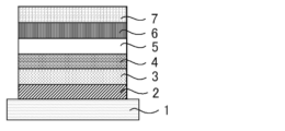
- An organic photoluminescence device has a structure in which at least a light-emitting layer is formed on a substrate.
- the organic electroluminescence element has a structure in which at least an anode, a cathode, and an organic layer are formed between the anode and the cathode.
- the organic layer includes at least a light-emitting layer, and may consist of only the light-emitting layer, or may have one or more organic layers in addition to the light-emitting layer.
- Such other organic layers can include hole transport layers, hole injection layers, electron blocking layers, hole blocking layers, electron injection layers, electron transport layers, exciton blocking layers, and the like.
- the hole transport layer may be a hole injection transport layer having a hole injection function
- the electron transport layer may be an electron injection transport layer having an electron injection function.
- the organic light-emitting device of the present invention is a multi-wavelength light-emitting organic light-emitting device
- the emission with the shortest wavelength may include delayed fluorescence.
- it is also possible that the emission with the shortest wavelength does not contain delayed fluorescence.
- An organic light-emitting device using the composition of the present invention when excited by thermal or electronic means, has a blue, green, yellow, orange, and red region (for example, 420-500 nm, 500 nm) in the ultraviolet region and the visible spectrum.
- organic light emitting devices can emit light in the red or orange region (eg, 620-780 nm).
- organic light emitting devices can emit light in the orange or yellow region (eg, 570-620 nm).
- an organic light emitting device can emit light in the green region (eg, 490-575 nm).
- an organic light emitting device can emit light in the blue region (eg, 400-490 nm).
- organic light emitting devices can emit light in the ultraviolet spectral region (eg, 280-400 nm).
- organic light emitting devices can emit light in the infrared spectral region (eg, 780 nm to 2 ⁇ m). It is preferable that the largest component of light emitted from the organic light-emitting device using the composition of the present invention is light emitted from the delayed fluorescence material contained in the composition of the present invention.
- Emission from the compound represented by the general formula (1) is preferably less than 10% of the light emission from the organic light-emitting device, for example, less than 1%, less than 0.1%, less than 0.01%, detection limit It may be below.
- Emission from the delayed fluorescence material may be, for example, greater than 50%, greater than 90%, greater than 99% of the emission from the organic light emitting device.
- the layer containing the composition of the present invention contains a fluorescent material as the third component
- the maximum component of light emitted from the organic light-emitting device may be light emitted from the fluorescent material.
- the emission from the luminescent material may be, for example, greater than 50%, greater than 90%, greater than 99% of the emission from the organic light emitting device.
- the organic electroluminescent device of the present invention is held by a substrate, which is not particularly limited and commonly used in organic electroluminescent devices such as glass, transparent plastic, quartz and silicon. Any material formed by
- the anode of the organic electroluminescent device is made from metals, alloys, conductive compounds, or combinations thereof.
- the metal, alloy or conductive compound has a high work function (4 eV or greater).
- the metal is Au.
- the conductive transparent material is selected from CuI, indium tin oxide (ITO), SnO2 and ZnO. Some embodiments use amorphous materials that can form transparent conductive films, such as IDIXO (In 2 O 3 —ZnO).
- the anode is a thin film. In some embodiments, the thin film is made by evaporation or sputtering.
- the film is patterned by photolithographic methods. In some embodiments, if the pattern does not need to be highly precise (eg, about 100 ⁇ m or greater), the pattern may be formed using a mask with a shape suitable for vapor deposition or sputtering onto the electrode material. In some embodiments, wet film forming methods such as printing and coating methods are used when coating materials such as organic conductive compounds can be applied.
- the anode has a transmittance of greater than 10% when emitted light passes through the anode, and the anode has a sheet resistance of several hundred ohms per unit area or less. In some embodiments, the thickness of the anode is 10-1,000 nm. In some embodiments, the thickness of the anode is 10-200 nm. In some embodiments, the thickness of the anode varies depending on the materials used.
- the cathode is made of electrode materials such as metals with a low work function (4 eV or less) (referred to as electron-injecting metals), alloys, conductive compounds, or combinations thereof.
- the electrode material is sodium, sodium-potassium alloys, magnesium, lithium, magnesium-copper mixtures, magnesium-silver mixtures, magnesium-aluminum mixtures, magnesium-indium mixtures, aluminum-aluminum oxide ( Al2 O 3 ) mixtures, indium, lithium-aluminum mixtures and rare earth elements.
- a mixture of an electron-injecting metal and a second metal that is a stable metal with a higher work function than the electron-injecting metal is used.
- the mixture is selected from magnesium-silver mixtures, magnesium-aluminum mixtures, magnesium-indium mixtures, aluminum-aluminum oxide (Al 2 O 3 ) mixtures, lithium-aluminum mixtures and aluminum. In some embodiments, the mixture improves electron injection properties and resistance to oxidation.
- the cathode is manufactured by depositing or sputtering the electrode material as a thin film. In some embodiments, the cathode has a sheet resistance of no more than several hundred ohms per unit area. In some embodiments, the thickness of said cathode is between 10 nm and 5 ⁇ m. In some embodiments, the thickness of the cathode is 50-200 nm.
- either one of the anode and cathode of the organic electroluminescent device is transparent or translucent to allow transmission of emitted light.
- transparent or translucent electroluminescent elements enhance light radiance.
- the cathode is formed of a conductive transparent material as described above for the anode, thereby forming a transparent or translucent cathode.
- the device includes an anode and a cathode, both transparent or translucent.
- the injection layer is the layer between the electrode and the organic layer. In some embodiments, the injection layer reduces drive voltage and enhances light radiance. In some embodiments, the injection layer comprises a hole injection layer and an electron injection layer. The injection layer can be placed between the anode and the light-emitting layer or hole-transporting layer and between the cathode and the light-emitting layer or electron-transporting layer. In some embodiments, an injection layer is present. In some embodiments, there is no injection layer. Preferred examples of compounds that can be used as the hole injection material are given below.
- a barrier layer is a layer that can prevent charges (electrons or holes) and/or excitons present in the light-emitting layer from diffusing out of the light-emitting layer.
- an electron blocking layer is between the light-emitting layer and the hole-transporting layer to block electrons from passing through the light-emitting layer to the hole-transporting layer.
- a hole blocking layer is between the emissive layer and the electron transport layer and blocks holes from passing through the emissive layer to the electron transport layer.
- the barrier layer prevents excitons from diffusing out of the emissive layer.
- the electron blocking layer and the hole blocking layer constitute an exciton blocking layer.
- the terms "electron blocking layer” or "exciton blocking layer” include layers that have the functionality of both an electron blocking layer and an exciton blocking layer.
- Hole blocking layer functions as an electron transport layer. In some embodiments, the hole blocking layer blocks holes from reaching the electron transport layer during electron transport. In some embodiments, the hole blocking layer increases the probability of recombination of electrons and holes in the emissive layer.
- the materials used for the hole blocking layer can be the same materials as described above for the electron transport layer. Preferred examples of compounds that can be used in the hole blocking layer are given below.
- Electron barrier layer The electron blocking layer transports holes. In some embodiments, the electron blocking layer prevents electrons from reaching the hole transport layer during hole transport. In some embodiments, the electron blocking layer increases the probability of recombination of electrons and holes in the emissive layer.
- the materials used for the electron blocking layer may be the same materials as described above for the hole transport layer. Specific examples of preferred compounds that can be used as the electron barrier material are given below.
- Exciton barrier layer The exciton blocking layer prevents diffusion of excitons generated through recombination of holes and electrons in the light emitting layer to the charge transport layer. In some embodiments, the exciton blocking layer allows effective confinement of excitons in the emissive layer. In some embodiments, the light emission efficiency of the device is improved. In some embodiments, an exciton blocking layer is adjacent to the emissive layer on either the anode side or the cathode side, and on both sides thereof. In some embodiments, when an exciton blocking layer is present on the anode side, it may be present between and adjacent to the hole-transporting layer and the light-emitting layer.
- an exciton blocking layer when an exciton blocking layer is present on the cathode side, it may be between and adjacent to the emissive layer and the cathode. In some embodiments, a hole-injection layer, electron-blocking layer, or similar layer is present between the anode and an exciton-blocking layer adjacent to the light-emitting layer on the anode side. In some embodiments, a hole injection layer, electron blocking layer, hole blocking layer or similar layer is present between the cathode and an exciton blocking layer adjacent to the emissive layer on the cathode side. In some embodiments, the exciton blocking layer comprises an excited singlet energy and an excited triplet energy, at least one of which is higher than the excited singlet energy and triplet energy, respectively, of the emissive material.
- the hole-transporting layer comprises a hole-transporting material.
- the hole transport layer is a single layer.
- the hole transport layer has multiple layers.
- the hole transport material has one property of a hole injection or transport property and an electron barrier property.
- the hole transport material is an organic material.
- the hole transport material is an inorganic material. Examples of known hole transport materials that can be used in the present invention include, but are not limited to, triazole derivatives, oxadiazole derivatives, imidazole derivatives, carbazole derivatives, indolocarbazole derivatives, polyarylalkane derivatives, pyrazoline derivatives, pyrazolones.
- the hole transport material is selected from porphyrin compounds, aromatic tertiary amine compounds and styrylamine compounds. In some embodiments, the hole transport material is an aromatic tertiary amine compound. Specific examples of preferred compounds that can be used as the hole-transporting material are given below.
- the electron transport layer includes an electron transport material.
- the electron transport layer is a single layer.
- the electron transport layer has multiple layers.
- the electron-transporting material need only function to transport electrons injected from the cathode to the emissive layer.
- the electron transport material also functions as a hole blocking material.
- electron-transporting layers examples include, but are not limited to, nitro-substituted fluorene derivatives, diphenylquinone derivatives, thiopyran dioxide derivatives, carbodiimides, fluorenylidene methane derivatives, anthraquinodimethanes, anthrone derivatives, oxazide Azole derivatives, azole derivatives, azine derivatives or combinations thereof, or polymers thereof.
- the electron transport material is a thiadiazole derivative or a quinoxaline derivative.
- the electron transport material is a polymeric material. Specific examples of preferred compounds that can be used as the electron-transporting material are given below.
- examples of preferred compounds as materials that can be added to each organic layer are given.
- it may be added as a stabilizing material.
- Preferred materials that can be used in organic electroluminescence elements are specifically exemplified, but materials that can be used in the present invention are not limitedly interpreted by the following exemplified compounds. Moreover, even compounds exemplified as materials having specific functions can be used as materials having other functions.
- the emissive layer is incorporated into the device.
- devices include, but are not limited to, OLED bulbs, OLED lamps, television displays, computer monitors, mobile phones and tablets.
- an electronic device includes an OLED having at least one organic layer including an anode, a cathode, and a light-emitting layer between the anode and the cathode.
- compositions described herein can be incorporated into various photosensitive or photoactivated devices, such as OLEDs or optoelectronic devices.
- the composition may be useful in facilitating charge or energy transfer within a device and/or as a hole transport material.
- OLEDs organic light emitting diodes
- OICs organic integrated circuits
- O-FETs organic field effect transistors
- O-TFTs organic thin film transistors
- O-LETs organic light emitting transistors
- O-SC organic solar cells.
- O-SC organic optical detectors
- O-FQD organic field-quench devices
- LOC luminescent fuel cells
- O-lasers organic laser diodes
- an electronic device includes an OLED including at least one organic layer including an anode, a cathode, and a light-emitting layer between the anode and the cathode.
- the device includes OLEDs of different colors.
- the device includes an array including combinations of OLEDs.
- said combination of OLEDs is a combination of three colors (eg RGB).
- the combination of OLEDs is a combination of colors other than red, green, and blue (eg, orange and yellow-green).
- said combination of OLEDs is a combination of two, four or more colors.
- the device a circuit board having a first side with a mounting surface and a second opposite side and defining at least one opening; at least one OLED on the mounting surface, wherein the at least one OLED is configured to emit light, wherein the at least one OLED includes at least one organic layer including an anode, a cathode, and a light-emitting layer between the anode and the cathode; at least one OLED comprising a housing for the circuit board; at least one connector disposed at an end of said housing, said housing and said connector defining a package suitable for attachment to a lighting fixture.
- the OLED light comprises multiple OLEDs mounted on a circuit board such that light is emitted in multiple directions. In some embodiments, some light emitted in the first direction is polarized and emitted in the second direction. In some embodiments, a reflector is used to polarize light emitted in the first direction.
- the emissive layers of the invention can be used in screens or displays.
- the compounds of the present invention are deposited onto a substrate using processes such as, but not limited to, vacuum evaporation, deposition, evaporation or chemical vapor deposition (CVD).
- the substrate is a photoplate structure useful in two-sided etching to provide unique aspect ratio pixels.
- Said screens also called masks
- the corresponding artwork pattern design allows placement of very steep narrow tie-bars between pixels in the vertical direction as well as large and wide beveled openings in the horizontal direction.
- the internal patterning of the pixels makes it possible to construct three-dimensional pixel openings with various aspect ratios in the horizontal and vertical directions. Further, the use of imaged "stripes" or halftone circles in pixel areas protects etching in specific areas until these specific patterns are undercut and removed from the substrate. All pixel areas are then treated with a similar etch rate, but their depth varies with the halftone pattern. Varying the size and spacing of the halftone patterns allows etching with varying degrees of protection within the pixel, allowing for the localized deep etching necessary to form steep vertical bevels. . A preferred material for the evaporation mask is Invar.
- Invar is a metal alloy that is cold rolled into long thin sheets in steel mills. Invar cannot be electrodeposited onto a spin mandrel as a nickel mask.
- a suitable and low-cost method for forming the open areas in the deposition mask is by wet chemical etching.
- the screen or display pattern is a matrix of pixels on a substrate.
- screen or display patterns are fabricated using lithography (eg, photolithography and e-beam lithography).
- the screen or display pattern is processed using wet chemical etching.
- the screen or display pattern is fabricated using plasma etching.
- An OLED display is generally manufactured by forming a large mother panel and then cutting the mother panel into cell panels.
- each cell panel on a mother panel is formed by forming a thin film transistor (TFT) having an active layer and source/drain electrodes on a base substrate, coating the TFT with a planarizing film, pixel electrodes, and a light emitting layer. , a counter electrode and an encapsulation layer, are sequentially formed and cut from the mother panel.
- TFT thin film transistor
- an organic light emitting diode (OLED) display comprising: forming a barrier layer on the base substrate of the mother panel; forming a plurality of display units on the barrier layer in cell panel units; forming an encapsulation layer over each of the display units of the cell panel; and applying an organic film to the interfaces between the cell panels.
- the barrier layer is an inorganic film, eg, made of SiNx, and the edges of the barrier layer are covered with an organic film, made of polyimide or acrylic.
- the organic film helps the mother panel to be softly cut into cell panels.
- a thin film transistor (TFT) layer has an emissive layer, a gate electrode, and source/drain electrodes.
- Each of the plurality of display units may have a thin film transistor (TFT) layer, a planarization film formed on the TFT layer, and a light emitting unit formed on the planarization film, and The applied organic film is made of the same material as that of the planarizing film, and is formed at the same time as the planarizing film is formed.
- the light-emitting unit is coupled with the TFT layer by a passivation layer, a planarizing film therebetween, and an encapsulation layer that covers and protects the light-emitting unit.
- the organic film is not connected to the display unit or encapsulation layer.
- each of the organic film and the planarizing film may include one of polyimide and acrylic.
- the barrier layer may be an inorganic film.
- the base substrate may be formed of polyimide.
- the method further includes attaching a carrier substrate made of a glass material to another surface of a base substrate made of polyimide before forming a barrier layer on the other surface of the base substrate; separating the carrier substrate from the base substrate prior to cutting along the interface.
- the OLED display is a flexible display.
- the passivation layer is an organic film placed on the TFT layer to cover the TFT layer.
- the planarizing film is an organic film formed over a passivation layer.
- the planarizing film is formed of polyimide or acrylic, as is the organic film formed on the edge of the barrier layer. In some embodiments, the planarizing film and the organic film are formed simultaneously during the manufacture of an OLED display. In some embodiments, the organic film may be formed on the edge of the barrier layer such that a portion of the organic film is in direct contact with the base substrate and a remaining portion of the organic film is , in contact with the barrier layer while surrounding the edges of the barrier layer.
- the emissive layer comprises a pixel electrode, a counter electrode, and an organic emissive layer disposed between the pixel electrode and the counter electrode.
- the pixel electrodes are connected to source/drain electrodes of the TFT layer.
- a suitable voltage is formed between the pixel electrode and the counter electrode, causing the organic light-emitting layer to emit light, thereby displaying an image. is formed.
- An image forming unit having a TFT layer and a light emitting unit is hereinafter referred to as a display unit.
- the encapsulation layer that covers the display unit and prevents the penetration of external moisture may be formed into a thin encapsulation structure in which organic films and inorganic films are alternately laminated.
- the encapsulation layer has a thin film-like encapsulation structure in which multiple thin films are stacked.
- the organic film applied to the interface portion is spaced apart from each of the plurality of display units.
- the organic film is formed such that a portion of the organic film is in direct contact with the base substrate and a remaining portion of the organic film is in contact with the barrier layer while surrounding the edges of the barrier layer. be done.
- the OLED display is flexible and uses a flexible base substrate made of polyimide.
- the base substrate is formed on a carrier substrate made of glass material, and then the carrier substrate is separated.
- a barrier layer is formed on the surface of the base substrate opposite the carrier substrate.
- the barrier layer is patterned according to the size of each cell panel. For example, a base substrate is formed on all surfaces of a mother panel, while barrier layers are formed according to the size of each cell panel, thereby forming grooves at the interfaces between the barrier layers of the cell panels. Each cell panel can be cut along the groove.
- the manufacturing method further comprises cutting along the interface, wherein a groove is formed in the barrier layer, at least a portion of the organic film is formed with the groove, and the groove is Does not penetrate the base substrate.
- a TFT layer of each cell panel is formed, and a passivation layer, which is an inorganic film, and a planarization film, which is an organic film, are placed on and cover the TFT layer.
- the planarizing film eg made of polyimide or acrylic
- the interface grooves are covered with an organic film, eg made of polyimide or acrylic. This prevents cracking by having the organic film absorb the impact that occurs when each cell panel is cut along the groove at the interface.
- the grooves at the interfaces between the barrier layers are coated with an organic film to absorb shocks that might otherwise be transmitted to the barrier layers, so that each cell panel is softly cut and the barrier layers It may prevent cracks from forming.
- the organic film covering the groove of the interface and the planarizing film are spaced apart from each other. For example, when the organic film and the planarizing film are connected to each other as a single layer, external moisture may enter the display unit through the planarizing film and the portion where the organic film remains. The organic film and planarizing film are spaced from each other such that the organic film is spaced from the display unit.
- the display unit is formed by forming a light-emitting unit and an encapsulating layer is placed over the display unit to cover the display unit.
- the carrier substrate carrying the base substrate is separated from the base substrate.
- the carrier substrate separates from the base substrate due to the difference in coefficient of thermal expansion between the carrier substrate and the base substrate.
- the mother panel is cut into cell panels.
- the mother panel is cut along the interfaces between the cell panels using a cutter.
- the interface groove along which the mother panel is cut is coated with an organic film so that the organic film absorbs impact during cutting.
- the barrier layer can be prevented from cracking during cutting. In some embodiments, the method reduces the reject rate of the product and stabilizes its quality.
- Another embodiment includes a barrier layer formed on a base substrate, a display unit formed on the barrier layer, an encapsulation layer formed on the display unit, and an organic layer applied to the edges of the barrier layer.
- An OLED display comprising a film.
- the features of the present invention will be more specifically described below with reference to Synthesis Examples and Examples.
- the materials, processing details, processing procedures, etc. described below can be changed as appropriate without departing from the gist of the present invention. Therefore, the scope of the present invention should not be construed to be limited by the specific examples shown below.
- the emission characteristics were evaluated using a source meter (manufactured by Keithley: 2400 series), a semiconductor parameter analyzer (manufactured by Agilent Technologies: E5273A), an optical power meter measuring device (manufactured by Newport: 1930C), and an optical spectrometer.
- reaction solution was cooled to room temperature and chloroform (300 mL) was added.
- the resulting organic layer was washed twice with water (300 mL), dried over magnesium sulfate, and the solvent was removed.
- Example 1 By laminating the following thin films at a degree of vacuum of 5.0 ⁇ 10 ⁇ 5 Pa by vacuum deposition on a glass substrate having an anode made of indium tin oxide (ITO) with a thickness of 50 nm.
- An organic electroluminescence device was produced.
- HAT-CN was formed to a thickness of 10 nm on ITO
- NPD was formed thereon to a thickness of 30 nm
- EBL1 was formed thereon to a thickness of 10 nm.
- the delayed fluorescence material (TADF21) and compound 2 were co-deposited from different vapor deposition sources to form a layer with a thickness of 40 nm to form a light-emitting layer.
- TADF21 delayed fluorescence material
- compound 2 were co-deposited from different vapor deposition sources to form a layer with a thickness of 40 nm to form a light-emitting layer.
- the content of the delayed fluorescence material was 35% by mass, and the content of Compound 2 was 65% by mass.
- Liq and SF3-TRZ were co-deposited from different vapor deposition sources to form a layer with a thickness of 30 nm.
- the contents of Liq and SF3-TRZ in this layer were 30 mass % and 70 mass %, respectively.
- Liq was formed to a thickness of 2 nm, and then aluminum (Al) was vapor-deposited to a thickness of 100 nm to form a cathode, thereby producing an organic electroluminescence device.
- This device was designated as EL device 1.
- Comparative EL device 1 was prepared by using comparative compound A instead of compound 2.
- EL device 1 present invention
- comparative EL device 1 comparative example
- Example 2 An organic electroluminescence device was produced in the same manner as in Example 1 except that TADF18 was used instead of TADF21 used in EL device 1 in Example 1. This element was designated as EL element 2 .
- An organic electroluminescence device was produced in the same manner by using comparative compound B instead of compound 2 used in EL device 2. This device was designated as a comparative EL device 2.
- Each organic electroluminescence device thus prepared was driven at a current density of 12.6 mA/cm 2 , and the time (LT95) was measured until the emission intensity reached 95% of that at the start of driving. As a result, when the LT95 of the EL element 2 was 1, the LT95 of the comparative EL element 2 was 0.6. From this, it was confirmed that when the compound represented by the general formula (1) was used, the life of the device was prolonged.
- Example 3 An organic electroluminescence device was produced in the same manner as in Example 1 except that TADF2 was used instead of TADF21 used in EL device 1 in Example 1. This element was designated as EL element 3. An organic electroluminescence device was produced in the same manner by using comparative compound B instead of compound 2 used in EL device 3. This element was designated as comparative EL element 3. Each organic electroluminescence element thus prepared was driven at a current density of 5.5 mA/cm 2 , and the time (LT95) was measured until the emission intensity reached 95% of that at the start of driving. As a result, when the LT95 of the EL element 3 was 1, the LT95 of the comparative EL element 3 was 0.8. From this, it was confirmed that when the compound represented by the general formula (1) was used, the life of the device was prolonged.
- Example 4 An organic electroluminescence device was produced in the same manner as in Example 1, except that Compound 2 was used in place of EBL1 used in Comparative EL device 1 (comparative example) in Example 1. Using this device as EL device 4, the drive voltage was measured at a current density of 6.3 mA/cm 2 in the same manner as in Example 1. The driving voltage of EL element 4 (present invention) was 0.23 V lower than the driving voltage of comparative EL element 1 (comparative example). From this, it was confirmed that the compound represented by the general formula (1) is also useful as an electron barrier material.
- Example 2 an organic electroluminescence device manufactured in the same manner as in Example 1 except that EBL1 used in Comparative EL device 1 (Comparative Example) in Example 1 was replaced with Reference Compound a was also compared. Although the driving voltage was lower than that of the EL element 1, it was not as high as that of the EL element 4, and there was a clear difference.
- Example 5 By laminating the following thin films at a degree of vacuum of 5.0 ⁇ 10 -5 Pa by a vacuum deposition method on a glass substrate on which an anode made of indium tin oxide (ITO) with a thickness of 50 nm is formed.
- An organic electroluminescence device was produced.
- HAT-CN was formed to a thickness of 10 nm on ITO
- NPD was formed thereon to a thickness of 30 nm
- Tris-PCz was formed thereon to a thickness of 10 nm.
- the delayed fluorescence material (TADF72) and the compound 74 were co-deposited from different vapor deposition sources to form a layer with a thickness of 40 nm to form a light-emitting layer.
- TADF72 delayed fluorescence material
- the compound 74 were co-deposited from different vapor deposition sources to form a layer with a thickness of 40 nm to form a light-emitting layer.
- the content of the delayed fluorescence material was 35% by mass, and the content of the compound 74 was 65% by mass.
- Liq and SF3-TRZ were co-deposited from different vapor deposition sources to form a layer with a thickness of 30 nm.
- the contents of Liq and SF3-TRZ in this layer were 30 mass % and 70 mass %, respectively.
- Liq was formed to a thickness of 2 nm, and then aluminum (Al) was vapor-deposited to a thickness of 100 nm to form a cathode, thereby producing an organic electroluminescence device. This element was designated as EL element 5 .
- Example 6 By laminating the following thin films at a degree of vacuum of 5.0 ⁇ 10 ⁇ 5 Pa by vacuum deposition on a glass substrate having an anode made of indium tin oxide (ITO) with a thickness of 50 nm.
- ITO indium tin oxide
- An organic electroluminescence device was produced.
- HAT-CN was formed on ITO to a thickness of 10 nm
- NPD was formed thereon to a thickness of 30 nm
- Compound 2 was formed thereon to a thickness of 10 nm.
- the delayed fluorescence material (TADF21) and comparative compound A were co-deposited from different vapor deposition sources to form a layer with a thickness of 40 nm to form a light-emitting layer.
- TADF21 delayed fluorescence material
- comparative compound A were co-deposited from different vapor deposition sources to form a layer with a thickness of 40 nm to form a light-emitting layer.
- the content of the delayed fluorescence material was 35% by mass, and the content of the comparative compound A was 65% by mass.
- Liq and SF3-TRZ were co-deposited from different vapor deposition sources to form a layer with a thickness of 30 nm.
- the contents of Liq and SF3-TRZ in this layer were 30 mass % and 70 mass %, respectively.
- Liq was formed to a thickness of 2 nm, and then aluminum (Al) was vapor-deposited to a thickness of 100 nm to form a cathode, thereby producing an organic electroluminescence device. This element was designated as EL element 8 .
- EL element 9 was manufactured using compound 30 instead of compound 2.
- Comparative EL device 5 was prepared by using comparative compound A instead of compound 2.
- the driving voltage and the external quantum efficiency (EQE) of each organic electroluminescence device prepared at a current density of 6.3 mA/cm 2 were measured.
- the results in the table confirm that the organic electroluminescence device using the compound represented by the general formula (1) as an electron barrier material has good electrical conductivity and achieves high luminous efficiency.
Landscapes
- Chemical & Material Sciences (AREA)
- Organic Chemistry (AREA)
- Engineering & Computer Science (AREA)
- Materials Engineering (AREA)
- Physics & Mathematics (AREA)
- Spectroscopy & Molecular Physics (AREA)
- Optics & Photonics (AREA)
- Nanotechnology (AREA)
- Electroluminescent Light Sources (AREA)
- Heterocyclic Carbon Compounds Containing A Hetero Ring Having Oxygen Or Sulfur (AREA)
Priority Applications (5)
| Application Number | Priority Date | Filing Date | Title |
|---|---|---|---|
| CN202280065043.0A CN118043317A (zh) | 2021-09-28 | 2022-08-31 | 化合物、组合物、主体材料、电子阻挡材料及有机发光元件 |
| EP22875707.6A EP4410789A4 (en) | 2021-09-28 | 2022-08-31 | COMPOUND, COMPOSITION, HOST MATERIAL, ELECTRON BARRIER MATERIAL AND ORGANIC LIGHT-EMITTING ELEMENT |
| US18/696,178 US20240391906A1 (en) | 2021-09-28 | 2022-08-31 | Compound, composition, host material, electron barrier material and organic light-emitting device |
| KR1020247010385A KR20240068663A (ko) | 2021-09-28 | 2022-08-31 | 화합물, 조성물, 호스트 재료, 전자 장벽 재료 및 유기 발광 소자 |
| JP2023550486A JPWO2023053835A1 (https=) | 2021-09-28 | 2022-08-31 |
Applications Claiming Priority (4)
| Application Number | Priority Date | Filing Date | Title |
|---|---|---|---|
| JP2021157765 | 2021-09-28 | ||
| JP2021-157765 | 2021-09-28 | ||
| JP2022-087873 | 2022-05-30 | ||
| JP2022087873 | 2022-05-30 |
Publications (1)
| Publication Number | Publication Date |
|---|---|
| WO2023053835A1 true WO2023053835A1 (ja) | 2023-04-06 |
Family
ID=85780624
Family Applications (1)
| Application Number | Title | Priority Date | Filing Date |
|---|---|---|---|
| PCT/JP2022/032781 Ceased WO2023053835A1 (ja) | 2021-09-28 | 2022-08-31 | 化合物、組成物、ホスト材料、電子障壁材料および有機発光素子 |
Country Status (6)
| Country | Link |
|---|---|
| US (1) | US20240391906A1 (https=) |
| EP (1) | EP4410789A4 (https=) |
| JP (1) | JPWO2023053835A1 (https=) |
| KR (1) | KR20240068663A (https=) |
| TW (1) | TW202330507A (https=) |
| WO (1) | WO2023053835A1 (https=) |
Cited By (1)
| Publication number | Priority date | Publication date | Assignee | Title |
|---|---|---|---|---|
| WO2024247998A1 (ja) * | 2023-05-29 | 2024-12-05 | 株式会社Kyulux | 有機エレクトロルミネッセンス素子、有機エレクトロルミネッセンス素子の設計方法およびプログラム |
Citations (51)
| Publication number | Priority date | Publication date | Assignee | Title |
|---|---|---|---|---|
| WO2013011954A1 (ja) | 2011-07-15 | 2013-01-24 | 国立大学法人九州大学 | 有機エレクトロルミネッセンス素子およびそれに用いる化合物 |
| WO2013011955A1 (ja) | 2011-07-15 | 2013-01-24 | 国立大学法人九州大学 | 遅延蛍光材料およびそれを用いた有機エレクトロルミネッセンス素子 |
| WO2013081088A1 (ja) | 2011-12-02 | 2013-06-06 | 国立大学法人九州大学 | 有機発光素子ならびにそれに用いる遅延蛍光材料および化合物 |
| JP2013116975A (ja) | 2011-12-02 | 2013-06-13 | Kyushu Univ | 遅延蛍光材料、有機発光素子および化合物 |
| WO2013133359A1 (ja) | 2012-03-09 | 2013-09-12 | 国立大学法人九州大学 | 発光材料および有機発光素子 |
| WO2013154064A1 (ja) | 2012-04-09 | 2013-10-17 | 国立大学法人九州大学 | 有機発光素子ならびにそれに用いる発光材料および化合物 |
| WO2013161437A1 (ja) | 2012-04-25 | 2013-10-31 | 国立大学法人九州大学 | 発光材料および有機発光素子 |
| JP2013253121A (ja) | 2011-07-15 | 2013-12-19 | Kyushu Univ | 遅延蛍光材料、それを用いた有機エレクトロルミネッセンス素子および化合物 |
| JP2013256490A (ja) | 2012-05-17 | 2013-12-26 | Kyushu Univ | 化合物、発光材料および有機発光素子 |
| JP2014009224A (ja) | 2012-07-03 | 2014-01-20 | Kyushu Univ | 発光材料、化合物および有機発光素子 |
| JP2014009352A (ja) | 2012-07-03 | 2014-01-20 | Kyushu Univ | 発光材料、化合物および有機発光素子 |
| WO2014034535A1 (ja) | 2012-08-30 | 2014-03-06 | 国立大学法人九州大学 | 発光材料、化合物、およびそれらを用いた有機発光素子 |
| WO2014115743A1 (ja) | 2013-01-23 | 2014-07-31 | 国立大学法人九州大学 | 発光材料およびそれを用いた有機発光素子 |
| WO2014122895A1 (ja) | 2013-02-07 | 2014-08-14 | 保土谷化学工業株式会社 | ジアザトリフェニレン環構造を有する化合物および有機エレクトロルミネッセンス素子 |
| WO2014126200A1 (ja) | 2013-02-18 | 2014-08-21 | 国立大学法人九州大学 | 化合物、発光材料および有機発光素子 |
| WO2014133121A1 (ja) | 2013-03-01 | 2014-09-04 | 国立大学法人九州大学 | 化合物、発光材料および有機発光素子 |
| WO2014136860A1 (ja) | 2013-03-08 | 2014-09-12 | 国立大学法人九州大学 | 化合物、発光材料および有機発光素子 |
| WO2014136758A1 (ja) | 2013-03-05 | 2014-09-12 | 国立大学法人九州大学 | 電荷輸送材料、ホスト材料、薄膜および有機発光素子 |
| WO2014168101A1 (ja) | 2013-04-10 | 2014-10-16 | 国立大学法人九州大学 | 発光材料、有機発光素子および化合物 |
| WO2014189122A1 (ja) | 2013-05-24 | 2014-11-27 | 国立大学法人九州大学 | 化合物、発光材料および有機発光素子 |
| WO2014196585A1 (ja) | 2013-06-05 | 2014-12-11 | 国立大学法人九州大学 | 発光材料、有機発光素子および化合物 |
| WO2014203840A1 (ja) | 2013-06-21 | 2014-12-24 | 国立大学法人九州大学 | 赤色発光材料、有機発光素子および化合物 |
| WO2015002213A1 (ja) | 2013-07-03 | 2015-01-08 | 国立大学法人九州大学 | 発光材料、遅延蛍光体、有機発光素子および化合物 |
| WO2015008580A1 (ja) | 2013-07-16 | 2015-01-22 | 国立大学法人九州大学 | 化合物、発光材料および有機発光素子 |
| WO2015016200A1 (ja) | 2013-08-01 | 2015-02-05 | 国立大学法人九州大学 | 化合物、発光材料および有機発光素子 |
| WO2015019725A1 (ja) | 2013-08-09 | 2015-02-12 | 国立大学法人九州大学 | 有機金属錯体、発光材料、遅延蛍光体および有機発光素子 |
| WO2015022974A1 (ja) | 2013-08-14 | 2015-02-19 | 国立大学法人九州大学 | 有機エレクトロルミネッセンス素子 |
| WO2015072470A1 (ja) | 2013-11-12 | 2015-05-21 | 国立大学法人九州大学 | 発光材料、並びに、これを用いた遅延蛍光体および有機発光素子 |
| WO2015072537A1 (ja) | 2013-11-18 | 2015-05-21 | 国立大学法人九州大学 | 発光材料、有機発光素子および化合物 |
| WO2015080183A1 (ja) | 2013-11-28 | 2015-06-04 | 国立大学法人九州大学 | 発光材料、有機発光素子および化合物 |
| WO2015080182A1 (ja) | 2013-11-28 | 2015-06-04 | 国立大学法人九州大学 | 発光材料、有機発光素子および化合物 |
| JP2015129240A (ja) | 2014-01-08 | 2015-07-16 | 国立大学法人九州大学 | 発光材料、有機発光素子および化合物 |
| JP2015520945A (ja) * | 2012-05-02 | 2015-07-23 | ローム・アンド・ハース・エレクトロニック・マテリアルズ・コリア・リミテッド | 新規有機エレクトロルミネセンス化合物およびそれを含む有機エレクトロルミネセンスデバイス |
| WO2015108049A1 (ja) | 2014-01-17 | 2015-07-23 | 国立大学法人九州大学 | 発光材料、有機発光素子および化合物 |
| WO2015129715A1 (ja) | 2014-02-28 | 2015-09-03 | 国立大学法人九州大学 | 発光材料、有機発光素子および化合物 |
| WO2015129714A1 (ja) | 2014-02-28 | 2015-09-03 | 国立大学法人九州大学 | 発光材料、有機発光素子および化合物 |
| WO2015133501A1 (ja) | 2014-03-07 | 2015-09-11 | 国立大学法人九州大学 | 発光材料、有機発光素子および化合物 |
| WO2015137136A1 (ja) | 2014-03-12 | 2015-09-17 | 国立大学法人九州大学 | 発光材料及びそれを用いた有機el素子 |
| WO2015137202A1 (ja) | 2014-03-11 | 2015-09-17 | 国立大学法人九州大学 | 有機発光素子、ホスト材料、発光材料および化合物 |
| WO2015137244A1 (ja) | 2014-03-11 | 2015-09-17 | 国立大学法人九州大学 | 発光材料、有機発光素子および化合物 |
| WO2015136880A1 (ja) | 2014-03-11 | 2015-09-17 | 保土谷化学工業株式会社 | アザフルオレン環構造を有するスピロ化合物、発光材料および有機エレクトロルミネッセンス素子 |
| WO2015146541A1 (ja) | 2014-03-27 | 2015-10-01 | 国立大学法人九州大学 | 発光材料、有機発光素子および化合物 |
| WO2015159541A1 (ja) | 2014-04-18 | 2015-10-22 | 保土谷化学工業株式会社 | テトラアザトリフェニレン環構造を有する化合物、発光材料および有機エレクトロルミネッセンス素子 |
| JP2017119663A (ja) | 2015-12-28 | 2017-07-06 | 株式会社Kyulux | 化合物、発光材料および有機発光素子 |
| JP2017119664A (ja) | 2015-12-28 | 2017-07-06 | 株式会社Kyulux | 化合物、発光材料および有機発光素子 |
| US20170346020A1 (en) * | 2015-05-22 | 2017-11-30 | Samsung Sdi Co., Ltd. | Compound for organic optoelectronic device, composition for organic optoelectronic device, and organic optoelectronic device and display device comprising same |
| JP2017222623A (ja) | 2016-06-17 | 2017-12-21 | 株式会社Kyulux | 化合物および有機発光素子 |
| JP2017226838A (ja) | 2016-06-17 | 2017-12-28 | 株式会社Kyulux | 発光材料、有機発光素子および化合物 |
| WO2018047853A1 (ja) | 2016-09-06 | 2018-03-15 | 株式会社Kyulux | 有機発光素子 |
| JP2018100411A (ja) | 2016-12-21 | 2018-06-28 | 国立大学法人九州大学 | 発光材料、化合物および有機発光素子 |
| JP7152805B1 (ja) * | 2021-09-28 | 2022-10-13 | 株式会社Kyulux | 化合物、組成物、ホスト材料、電子障壁材料および有機発光素子 |
Family Cites Families (1)
| Publication number | Priority date | Publication date | Assignee | Title |
|---|---|---|---|---|
| KR102816740B1 (ko) * | 2018-06-22 | 2025-06-10 | 듀폰스페셜티머터리얼스코리아 유한회사 | 복수 종의 호스트 재료 및 이를 포함하는 유기 전계 발광 소자 |
-
2022
- 2022-08-31 EP EP22875707.6A patent/EP4410789A4/en not_active Withdrawn
- 2022-08-31 JP JP2023550486A patent/JPWO2023053835A1/ja active Pending
- 2022-08-31 US US18/696,178 patent/US20240391906A1/en active Pending
- 2022-08-31 KR KR1020247010385A patent/KR20240068663A/ko active Pending
- 2022-08-31 WO PCT/JP2022/032781 patent/WO2023053835A1/ja not_active Ceased
- 2022-09-02 TW TW111133295A patent/TW202330507A/zh unknown
Patent Citations (51)
| Publication number | Priority date | Publication date | Assignee | Title |
|---|---|---|---|---|
| WO2013011954A1 (ja) | 2011-07-15 | 2013-01-24 | 国立大学法人九州大学 | 有機エレクトロルミネッセンス素子およびそれに用いる化合物 |
| WO2013011955A1 (ja) | 2011-07-15 | 2013-01-24 | 国立大学法人九州大学 | 遅延蛍光材料およびそれを用いた有機エレクトロルミネッセンス素子 |
| JP2013253121A (ja) | 2011-07-15 | 2013-12-19 | Kyushu Univ | 遅延蛍光材料、それを用いた有機エレクトロルミネッセンス素子および化合物 |
| WO2013081088A1 (ja) | 2011-12-02 | 2013-06-06 | 国立大学法人九州大学 | 有機発光素子ならびにそれに用いる遅延蛍光材料および化合物 |
| JP2013116975A (ja) | 2011-12-02 | 2013-06-13 | Kyushu Univ | 遅延蛍光材料、有機発光素子および化合物 |
| WO2013133359A1 (ja) | 2012-03-09 | 2013-09-12 | 国立大学法人九州大学 | 発光材料および有機発光素子 |
| WO2013154064A1 (ja) | 2012-04-09 | 2013-10-17 | 国立大学法人九州大学 | 有機発光素子ならびにそれに用いる発光材料および化合物 |
| WO2013161437A1 (ja) | 2012-04-25 | 2013-10-31 | 国立大学法人九州大学 | 発光材料および有機発光素子 |
| JP2015520945A (ja) * | 2012-05-02 | 2015-07-23 | ローム・アンド・ハース・エレクトロニック・マテリアルズ・コリア・リミテッド | 新規有機エレクトロルミネセンス化合物およびそれを含む有機エレクトロルミネセンスデバイス |
| JP2013256490A (ja) | 2012-05-17 | 2013-12-26 | Kyushu Univ | 化合物、発光材料および有機発光素子 |
| JP2014009224A (ja) | 2012-07-03 | 2014-01-20 | Kyushu Univ | 発光材料、化合物および有機発光素子 |
| JP2014009352A (ja) | 2012-07-03 | 2014-01-20 | Kyushu Univ | 発光材料、化合物および有機発光素子 |
| WO2014034535A1 (ja) | 2012-08-30 | 2014-03-06 | 国立大学法人九州大学 | 発光材料、化合物、およびそれらを用いた有機発光素子 |
| WO2014115743A1 (ja) | 2013-01-23 | 2014-07-31 | 国立大学法人九州大学 | 発光材料およびそれを用いた有機発光素子 |
| WO2014122895A1 (ja) | 2013-02-07 | 2014-08-14 | 保土谷化学工業株式会社 | ジアザトリフェニレン環構造を有する化合物および有機エレクトロルミネッセンス素子 |
| WO2014126200A1 (ja) | 2013-02-18 | 2014-08-21 | 国立大学法人九州大学 | 化合物、発光材料および有機発光素子 |
| WO2014133121A1 (ja) | 2013-03-01 | 2014-09-04 | 国立大学法人九州大学 | 化合物、発光材料および有機発光素子 |
| WO2014136758A1 (ja) | 2013-03-05 | 2014-09-12 | 国立大学法人九州大学 | 電荷輸送材料、ホスト材料、薄膜および有機発光素子 |
| WO2014136860A1 (ja) | 2013-03-08 | 2014-09-12 | 国立大学法人九州大学 | 化合物、発光材料および有機発光素子 |
| WO2014168101A1 (ja) | 2013-04-10 | 2014-10-16 | 国立大学法人九州大学 | 発光材料、有機発光素子および化合物 |
| WO2014189122A1 (ja) | 2013-05-24 | 2014-11-27 | 国立大学法人九州大学 | 化合物、発光材料および有機発光素子 |
| WO2014196585A1 (ja) | 2013-06-05 | 2014-12-11 | 国立大学法人九州大学 | 発光材料、有機発光素子および化合物 |
| WO2014203840A1 (ja) | 2013-06-21 | 2014-12-24 | 国立大学法人九州大学 | 赤色発光材料、有機発光素子および化合物 |
| WO2015002213A1 (ja) | 2013-07-03 | 2015-01-08 | 国立大学法人九州大学 | 発光材料、遅延蛍光体、有機発光素子および化合物 |
| WO2015008580A1 (ja) | 2013-07-16 | 2015-01-22 | 国立大学法人九州大学 | 化合物、発光材料および有機発光素子 |
| WO2015016200A1 (ja) | 2013-08-01 | 2015-02-05 | 国立大学法人九州大学 | 化合物、発光材料および有機発光素子 |
| WO2015019725A1 (ja) | 2013-08-09 | 2015-02-12 | 国立大学法人九州大学 | 有機金属錯体、発光材料、遅延蛍光体および有機発光素子 |
| WO2015022974A1 (ja) | 2013-08-14 | 2015-02-19 | 国立大学法人九州大学 | 有機エレクトロルミネッセンス素子 |
| WO2015072470A1 (ja) | 2013-11-12 | 2015-05-21 | 国立大学法人九州大学 | 発光材料、並びに、これを用いた遅延蛍光体および有機発光素子 |
| WO2015072537A1 (ja) | 2013-11-18 | 2015-05-21 | 国立大学法人九州大学 | 発光材料、有機発光素子および化合物 |
| WO2015080183A1 (ja) | 2013-11-28 | 2015-06-04 | 国立大学法人九州大学 | 発光材料、有機発光素子および化合物 |
| WO2015080182A1 (ja) | 2013-11-28 | 2015-06-04 | 国立大学法人九州大学 | 発光材料、有機発光素子および化合物 |
| JP2015129240A (ja) | 2014-01-08 | 2015-07-16 | 国立大学法人九州大学 | 発光材料、有機発光素子および化合物 |
| WO2015108049A1 (ja) | 2014-01-17 | 2015-07-23 | 国立大学法人九州大学 | 発光材料、有機発光素子および化合物 |
| WO2015129715A1 (ja) | 2014-02-28 | 2015-09-03 | 国立大学法人九州大学 | 発光材料、有機発光素子および化合物 |
| WO2015129714A1 (ja) | 2014-02-28 | 2015-09-03 | 国立大学法人九州大学 | 発光材料、有機発光素子および化合物 |
| WO2015133501A1 (ja) | 2014-03-07 | 2015-09-11 | 国立大学法人九州大学 | 発光材料、有機発光素子および化合物 |
| WO2015137202A1 (ja) | 2014-03-11 | 2015-09-17 | 国立大学法人九州大学 | 有機発光素子、ホスト材料、発光材料および化合物 |
| WO2015137244A1 (ja) | 2014-03-11 | 2015-09-17 | 国立大学法人九州大学 | 発光材料、有機発光素子および化合物 |
| WO2015136880A1 (ja) | 2014-03-11 | 2015-09-17 | 保土谷化学工業株式会社 | アザフルオレン環構造を有するスピロ化合物、発光材料および有機エレクトロルミネッセンス素子 |
| WO2015137136A1 (ja) | 2014-03-12 | 2015-09-17 | 国立大学法人九州大学 | 発光材料及びそれを用いた有機el素子 |
| WO2015146541A1 (ja) | 2014-03-27 | 2015-10-01 | 国立大学法人九州大学 | 発光材料、有機発光素子および化合物 |
| WO2015159541A1 (ja) | 2014-04-18 | 2015-10-22 | 保土谷化学工業株式会社 | テトラアザトリフェニレン環構造を有する化合物、発光材料および有機エレクトロルミネッセンス素子 |
| US20170346020A1 (en) * | 2015-05-22 | 2017-11-30 | Samsung Sdi Co., Ltd. | Compound for organic optoelectronic device, composition for organic optoelectronic device, and organic optoelectronic device and display device comprising same |
| JP2017119663A (ja) | 2015-12-28 | 2017-07-06 | 株式会社Kyulux | 化合物、発光材料および有機発光素子 |
| JP2017119664A (ja) | 2015-12-28 | 2017-07-06 | 株式会社Kyulux | 化合物、発光材料および有機発光素子 |
| JP2017222623A (ja) | 2016-06-17 | 2017-12-21 | 株式会社Kyulux | 化合物および有機発光素子 |
| JP2017226838A (ja) | 2016-06-17 | 2017-12-28 | 株式会社Kyulux | 発光材料、有機発光素子および化合物 |
| WO2018047853A1 (ja) | 2016-09-06 | 2018-03-15 | 株式会社Kyulux | 有機発光素子 |
| JP2018100411A (ja) | 2016-12-21 | 2018-06-28 | 国立大学法人九州大学 | 発光材料、化合物および有機発光素子 |
| JP7152805B1 (ja) * | 2021-09-28 | 2022-10-13 | 株式会社Kyulux | 化合物、組成物、ホスト材料、電子障壁材料および有機発光素子 |
Non-Patent Citations (3)
| Title |
|---|
| H. UOYAMA ET AL., NATURE, vol. 492, 2012, pages 234 - 238 |
| K. MASUI ET AL., ORG. ELECTRON, vol. 14, 2013, pages 2721 |
| See also references of EP4410789A4 |
Cited By (1)
| Publication number | Priority date | Publication date | Assignee | Title |
|---|---|---|---|---|
| WO2024247998A1 (ja) * | 2023-05-29 | 2024-12-05 | 株式会社Kyulux | 有機エレクトロルミネッセンス素子、有機エレクトロルミネッセンス素子の設計方法およびプログラム |
Also Published As
| Publication number | Publication date |
|---|---|
| KR20240068663A (ko) | 2024-05-17 |
| EP4410789A1 (en) | 2024-08-07 |
| US20240391906A1 (en) | 2024-11-28 |
| TW202330507A (zh) | 2023-08-01 |
| EP4410789A4 (en) | 2025-01-22 |
| JPWO2023053835A1 (https=) | 2023-04-06 |
Similar Documents
| Publication | Publication Date | Title |
|---|---|---|
| JP7594794B2 (ja) | ホスト材料、組成物および有機発光素子 | |
| WO2022249505A1 (ja) | 化合物、発光材料および発光素子 | |
| WO2023140130A1 (ja) | 化合物、発光材料および有機発光素子 | |
| WO2022168956A1 (ja) | 化合物、発光材料および有機発光素子 | |
| JP2023032402A (ja) | 化合物、発光材料および有機発光素子 | |
| JP7152805B1 (ja) | 化合物、組成物、ホスト材料、電子障壁材料および有機発光素子 | |
| WO2023053835A1 (ja) | 化合物、組成物、ホスト材料、電子障壁材料および有機発光素子 | |
| WO2022230574A1 (ja) | 電荷輸送材料、組成物および有機発光素子 | |
| KR20250096835A (ko) | 화합물, 발광 재료 및 발광 소자 | |
| WO2022270591A1 (ja) | 化合物、組成物、ホスト材料、電子障壁材料および有機発光素子 | |
| KR20240017808A (ko) | 화합물, 발광 재료 및 발광 소자 | |
| JP7722697B2 (ja) | 化合物、組成物、ホスト材料および有機発光素子 | |
| JP7780178B2 (ja) | 化合物、組成物、ホスト材料および有機発光素子 | |
| JP7764013B2 (ja) | 電荷輸送材料、組成物および有機発光素子 | |
| JP7724529B2 (ja) | 化合物、発光材料および有機発光素子 | |
| JP7780183B2 (ja) | 化合物、組成物、ホスト材料および有機発光素子 | |
| WO2023112808A1 (ja) | 化合物、ホスト材料、電子障壁材料、組成物および有機発光素子 | |
| JP2023159034A (ja) | 化合物、ホスト材料、組成物および有機発光素子 | |
| CN118043317A (zh) | 化合物、组合物、主体材料、电子阻挡材料及有机发光元件 | |
| JP2024134014A (ja) | 化合物、ホスト材料、組成物および有機発光素子 | |
| KR20240069637A (ko) | 화합물, 발광 재료 및 유기 발광 소자 | |
| CN118382621A (zh) | 化合物、主体材料、电子阻挡材料、组合物及有机发光元件 | |
| JP2024176516A (ja) | 化合物、発光材料および有機発光素子 | |
| JP2024070787A (ja) | 化合物、発光材料および有機発光素子 | |
| WO2023276918A1 (ja) | 化合物、電子障壁材料、有機半導体素子および化合物 |
Legal Events
| Date | Code | Title | Description |
|---|---|---|---|
| 121 | Ep: the epo has been informed by wipo that ep was designated in this application |
Ref document number: 22875707 Country of ref document: EP Kind code of ref document: A1 |
|
| WWE | Wipo information: entry into national phase |
Ref document number: 2023550486 Country of ref document: JP |
|
| WWE | Wipo information: entry into national phase |
Ref document number: 202280065043.0 Country of ref document: CN |
|
| ENP | Entry into the national phase |
Ref document number: 20247010385 Country of ref document: KR Kind code of ref document: A |
|
| WWE | Wipo information: entry into national phase |
Ref document number: 18696178 Country of ref document: US |
|
| NENP | Non-entry into the national phase |
Ref country code: DE |
|
| ENP | Entry into the national phase |
Ref document number: 2022875707 Country of ref document: EP Effective date: 20240429 |
|
| WWW | Wipo information: withdrawn in national office |
Ref document number: 2022875707 Country of ref document: EP |