WO2023033126A1 - リードフレーム及びその製造方法 - Google Patents
リードフレーム及びその製造方法 Download PDFInfo
- Publication number
- WO2023033126A1 WO2023033126A1 PCT/JP2022/033037 JP2022033037W WO2023033126A1 WO 2023033126 A1 WO2023033126 A1 WO 2023033126A1 JP 2022033037 W JP2022033037 W JP 2022033037W WO 2023033126 A1 WO2023033126 A1 WO 2023033126A1
- Authority
- WO
- WIPO (PCT)
- Prior art keywords
- lead
- die pad
- rough
- metal substrate
- lead frame
- Prior art date
- Legal status (The legal status is an assumption and is not a legal conclusion. Google has not performed a legal analysis and makes no representation as to the accuracy of the status listed.)
- Ceased
Links
Images


Classifications
-
- H—ELECTRICITY
- H10—SEMICONDUCTOR DEVICES; ELECTRIC SOLID-STATE DEVICES NOT OTHERWISE PROVIDED FOR
- H10W—GENERIC PACKAGES, INTERCONNECTIONS, CONNECTORS OR OTHER CONSTRUCTIONAL DETAILS OF DEVICES COVERED BY CLASS H10
- H10W70/00—Package substrates; Interposers; Redistribution layers [RDL]
- H10W70/40—Leadframes
- H10W70/421—Shapes or dispositions
- H10W70/424—Cross-sectional shapes
-
- H—ELECTRICITY
- H10—SEMICONDUCTOR DEVICES; ELECTRIC SOLID-STATE DEVICES NOT OTHERWISE PROVIDED FOR
- H10W—GENERIC PACKAGES, INTERCONNECTIONS, CONNECTORS OR OTHER CONSTRUCTIONAL DETAILS OF DEVICES COVERED BY CLASS H10
- H10W42/00—Arrangements for protection of devices
-
- H—ELECTRICITY
- H10—SEMICONDUCTOR DEVICES; ELECTRIC SOLID-STATE DEVICES NOT OTHERWISE PROVIDED FOR
- H10W—GENERIC PACKAGES, INTERCONNECTIONS, CONNECTORS OR OTHER CONSTRUCTIONAL DETAILS OF DEVICES COVERED BY CLASS H10
- H10W70/00—Package substrates; Interposers; Redistribution layers [RDL]
- H10W70/01—Manufacture or treatment
- H10W70/04—Manufacture or treatment of leadframes
- H10W70/042—Etching
-
- H—ELECTRICITY
- H10—SEMICONDUCTOR DEVICES; ELECTRIC SOLID-STATE DEVICES NOT OTHERWISE PROVIDED FOR
- H10W—GENERIC PACKAGES, INTERCONNECTIONS, CONNECTORS OR OTHER CONSTRUCTIONAL DETAILS OF DEVICES COVERED BY CLASS H10
- H10W70/00—Package substrates; Interposers; Redistribution layers [RDL]
- H10W70/01—Manufacture or treatment
- H10W70/04—Manufacture or treatment of leadframes
- H10W70/048—Mechanical treatments, e.g. punching, cutting, deforming or cold welding
-
- H—ELECTRICITY
- H10—SEMICONDUCTOR DEVICES; ELECTRIC SOLID-STATE DEVICES NOT OTHERWISE PROVIDED FOR
- H10W—GENERIC PACKAGES, INTERCONNECTIONS, CONNECTORS OR OTHER CONSTRUCTIONAL DETAILS OF DEVICES COVERED BY CLASS H10
- H10W70/00—Package substrates; Interposers; Redistribution layers [RDL]
- H10W70/40—Leadframes
- H10W70/411—Chip-supporting parts, e.g. die pads
- H10W70/417—Bonding materials between chips and die pads
-
- H—ELECTRICITY
- H10—SEMICONDUCTOR DEVICES; ELECTRIC SOLID-STATE DEVICES NOT OTHERWISE PROVIDED FOR
- H10W—GENERIC PACKAGES, INTERCONNECTIONS, CONNECTORS OR OTHER CONSTRUCTIONAL DETAILS OF DEVICES COVERED BY CLASS H10
- H10W70/00—Package substrates; Interposers; Redistribution layers [RDL]
- H10W70/40—Leadframes
- H10W70/421—Shapes or dispositions
-
- H—ELECTRICITY
- H10—SEMICONDUCTOR DEVICES; ELECTRIC SOLID-STATE DEVICES NOT OTHERWISE PROVIDED FOR
- H10W—GENERIC PACKAGES, INTERCONNECTIONS, CONNECTORS OR OTHER CONSTRUCTIONAL DETAILS OF DEVICES COVERED BY CLASS H10
- H10W70/00—Package substrates; Interposers; Redistribution layers [RDL]
- H10W70/40—Leadframes
- H10W70/456—Materials
- H10W70/457—Materials of metallic layers on leadframes
-
- H—ELECTRICITY
- H10—SEMICONDUCTOR DEVICES; ELECTRIC SOLID-STATE DEVICES NOT OTHERWISE PROVIDED FOR
- H10W—GENERIC PACKAGES, INTERCONNECTIONS, CONNECTORS OR OTHER CONSTRUCTIONAL DETAILS OF DEVICES COVERED BY CLASS H10
- H10W70/00—Package substrates; Interposers; Redistribution layers [RDL]
- H10W70/40—Leadframes
- H10W70/464—Additional interconnections in combination with leadframes
- H10W70/465—Bumps or wires
-
- H—ELECTRICITY
- H10—SEMICONDUCTOR DEVICES; ELECTRIC SOLID-STATE DEVICES NOT OTHERWISE PROVIDED FOR
- H10W—GENERIC PACKAGES, INTERCONNECTIONS, CONNECTORS OR OTHER CONSTRUCTIONAL DETAILS OF DEVICES COVERED BY CLASS H10
- H10W72/00—Interconnections or connectors in packages
-
- H—ELECTRICITY
- H10—SEMICONDUCTOR DEVICES; ELECTRIC SOLID-STATE DEVICES NOT OTHERWISE PROVIDED FOR
- H10W—GENERIC PACKAGES, INTERCONNECTIONS, CONNECTORS OR OTHER CONSTRUCTIONAL DETAILS OF DEVICES COVERED BY CLASS H10
- H10W72/00—Interconnections or connectors in packages
- H10W72/071—Connecting or disconnecting
-
- H—ELECTRICITY
- H10—SEMICONDUCTOR DEVICES; ELECTRIC SOLID-STATE DEVICES NOT OTHERWISE PROVIDED FOR
- H10W—GENERIC PACKAGES, INTERCONNECTIONS, CONNECTORS OR OTHER CONSTRUCTIONAL DETAILS OF DEVICES COVERED BY CLASS H10
- H10W74/00—Encapsulations, e.g. protective coatings
- H10W74/01—Manufacture or treatment
- H10W74/014—Manufacture or treatment using batch processing
-
- H—ELECTRICITY
- H10—SEMICONDUCTOR DEVICES; ELECTRIC SOLID-STATE DEVICES NOT OTHERWISE PROVIDED FOR
- H10W—GENERIC PACKAGES, INTERCONNECTIONS, CONNECTORS OR OTHER CONSTRUCTIONAL DETAILS OF DEVICES COVERED BY CLASS H10
- H10W74/00—Encapsulations, e.g. protective coatings
- H10W74/10—Encapsulations, e.g. protective coatings characterised by their shape or disposition
- H10W74/111—Encapsulations, e.g. protective coatings characterised by their shape or disposition the semiconductor body being completely enclosed
- H10W74/127—Encapsulations, e.g. protective coatings characterised by their shape or disposition the semiconductor body being completely enclosed characterised by arrangements for sealing or adhesion
-
- H—ELECTRICITY
- H10—SEMICONDUCTOR DEVICES; ELECTRIC SOLID-STATE DEVICES NOT OTHERWISE PROVIDED FOR
- H10W—GENERIC PACKAGES, INTERCONNECTIONS, CONNECTORS OR OTHER CONSTRUCTIONAL DETAILS OF DEVICES COVERED BY CLASS H10
- H10W90/00—Package configurations
- H10W90/811—Multiple chips on leadframes
-
- C—CHEMISTRY; METALLURGY
- C23—COATING METALLIC MATERIAL; COATING MATERIAL WITH METALLIC MATERIAL; CHEMICAL SURFACE TREATMENT; DIFFUSION TREATMENT OF METALLIC MATERIAL; COATING BY VACUUM EVAPORATION, BY SPUTTERING, BY ION IMPLANTATION OR BY CHEMICAL VAPOUR DEPOSITION, IN GENERAL; INHIBITING CORROSION OF METALLIC MATERIAL OR INCRUSTATION IN GENERAL
- C23C—COATING METALLIC MATERIAL; COATING MATERIAL WITH METALLIC MATERIAL; SURFACE TREATMENT OF METALLIC MATERIAL BY DIFFUSION INTO THE SURFACE, BY CHEMICAL CONVERSION OR SUBSTITUTION; COATING BY VACUUM EVAPORATION, BY SPUTTERING, BY ION IMPLANTATION OR BY CHEMICAL VAPOUR DEPOSITION, IN GENERAL
- C23C18/00—Chemical coating by decomposition of either liquid compounds or solutions of the coating forming compounds, without leaving reaction products of surface material in the coating; Contact plating
- C23C18/16—Chemical coating by decomposition of either liquid compounds or solutions of the coating forming compounds, without leaving reaction products of surface material in the coating; Contact plating by reduction or substitution, e.g. electroless plating
- C23C18/18—Pretreatment of the material to be coated
- C23C18/20—Pretreatment of the material to be coated of organic surfaces, e.g. resins
- C23C18/22—Roughening, e.g. by etching
-
- H—ELECTRICITY
- H05—ELECTRIC TECHNIQUES NOT OTHERWISE PROVIDED FOR
- H05K—PRINTED CIRCUITS; CASINGS OR CONSTRUCTIONAL DETAILS OF ELECTRIC APPARATUS; MANUFACTURE OF ASSEMBLAGES OF ELECTRICAL COMPONENTS
- H05K2203/00—Indexing scheme relating to apparatus or processes for manufacturing printed circuits covered by H05K3/00
- H05K2203/03—Metal processing
- H05K2203/0307—Providing micro- or nanometer scale roughness on a metal surface, e.g. by plating of nodules or dendrites
-
- H—ELECTRICITY
- H10—SEMICONDUCTOR DEVICES; ELECTRIC SOLID-STATE DEVICES NOT OTHERWISE PROVIDED FOR
- H10W—GENERIC PACKAGES, INTERCONNECTIONS, CONNECTORS OR OTHER CONSTRUCTIONAL DETAILS OF DEVICES COVERED BY CLASS H10
- H10W70/00—Package substrates; Interposers; Redistribution layers [RDL]
- H10W70/40—Leadframes
- H10W70/453—Leadframes comprising flexible metallic tapes
-
- H—ELECTRICITY
- H10—SEMICONDUCTOR DEVICES; ELECTRIC SOLID-STATE DEVICES NOT OTHERWISE PROVIDED FOR
- H10W—GENERIC PACKAGES, INTERCONNECTIONS, CONNECTORS OR OTHER CONSTRUCTIONAL DETAILS OF DEVICES COVERED BY CLASS H10
- H10W72/00—Interconnections or connectors in packages
- H10W72/01—Manufacture or treatment
- H10W72/0198—Manufacture or treatment batch processes
-
- H—ELECTRICITY
- H10—SEMICONDUCTOR DEVICES; ELECTRIC SOLID-STATE DEVICES NOT OTHERWISE PROVIDED FOR
- H10W—GENERIC PACKAGES, INTERCONNECTIONS, CONNECTORS OR OTHER CONSTRUCTIONAL DETAILS OF DEVICES COVERED BY CLASS H10
- H10W72/00—Interconnections or connectors in packages
- H10W72/071—Connecting or disconnecting
- H10W72/072—Connecting or disconnecting of bump connectors
- H10W72/07251—Connecting or disconnecting of bump connectors characterised by changes in properties of the bump connectors during connecting
-
- H—ELECTRICITY
- H10—SEMICONDUCTOR DEVICES; ELECTRIC SOLID-STATE DEVICES NOT OTHERWISE PROVIDED FOR
- H10W—GENERIC PACKAGES, INTERCONNECTIONS, CONNECTORS OR OTHER CONSTRUCTIONAL DETAILS OF DEVICES COVERED BY CLASS H10
- H10W72/00—Interconnections or connectors in packages
- H10W72/20—Bump connectors, e.g. solder bumps or copper pillars; Dummy bumps; Thermal bumps
-
- H—ELECTRICITY
- H10—SEMICONDUCTOR DEVICES; ELECTRIC SOLID-STATE DEVICES NOT OTHERWISE PROVIDED FOR
- H10W—GENERIC PACKAGES, INTERCONNECTIONS, CONNECTORS OR OTHER CONSTRUCTIONAL DETAILS OF DEVICES COVERED BY CLASS H10
- H10W72/00—Interconnections or connectors in packages
- H10W72/50—Bond wires
- H10W72/541—Dispositions of bond wires
- H10W72/5449—Dispositions of bond wires not being orthogonal to a side surface of the chip, e.g. fan-out arrangements
-
- H—ELECTRICITY
- H10—SEMICONDUCTOR DEVICES; ELECTRIC SOLID-STATE DEVICES NOT OTHERWISE PROVIDED FOR
- H10W—GENERIC PACKAGES, INTERCONNECTIONS, CONNECTORS OR OTHER CONSTRUCTIONAL DETAILS OF DEVICES COVERED BY CLASS H10
- H10W72/00—Interconnections or connectors in packages
- H10W72/851—Dispositions of multiple connectors or interconnections
- H10W72/874—On different surfaces
- H10W72/884—Die-attach connectors and bond wires
-
- H—ELECTRICITY
- H10—SEMICONDUCTOR DEVICES; ELECTRIC SOLID-STATE DEVICES NOT OTHERWISE PROVIDED FOR
- H10W—GENERIC PACKAGES, INTERCONNECTIONS, CONNECTORS OR OTHER CONSTRUCTIONAL DETAILS OF DEVICES COVERED BY CLASS H10
- H10W72/00—Interconnections or connectors in packages
- H10W72/90—Bond pads, in general
- H10W72/931—Shapes of bond pads
- H10W72/932—Plan-view shape, i.e. in top view
-
- H—ELECTRICITY
- H10—SEMICONDUCTOR DEVICES; ELECTRIC SOLID-STATE DEVICES NOT OTHERWISE PROVIDED FOR
- H10W—GENERIC PACKAGES, INTERCONNECTIONS, CONNECTORS OR OTHER CONSTRUCTIONAL DETAILS OF DEVICES COVERED BY CLASS H10
- H10W74/00—Encapsulations, e.g. protective coatings
-
- H—ELECTRICITY
- H10—SEMICONDUCTOR DEVICES; ELECTRIC SOLID-STATE DEVICES NOT OTHERWISE PROVIDED FOR
- H10W—GENERIC PACKAGES, INTERCONNECTIONS, CONNECTORS OR OTHER CONSTRUCTIONAL DETAILS OF DEVICES COVERED BY CLASS H10
- H10W74/00—Encapsulations, e.g. protective coatings
- H10W74/10—Encapsulations, e.g. protective coatings characterised by their shape or disposition
- H10W74/111—Encapsulations, e.g. protective coatings characterised by their shape or disposition the semiconductor body being completely enclosed
-
- H—ELECTRICITY
- H10—SEMICONDUCTOR DEVICES; ELECTRIC SOLID-STATE DEVICES NOT OTHERWISE PROVIDED FOR
- H10W—GENERIC PACKAGES, INTERCONNECTIONS, CONNECTORS OR OTHER CONSTRUCTIONAL DETAILS OF DEVICES COVERED BY CLASS H10
- H10W90/00—Package configurations
- H10W90/701—Package configurations characterised by the relative positions of pads or connectors relative to package parts
- H10W90/721—Package configurations characterised by the relative positions of pads or connectors relative to package parts of bump connectors
- H10W90/726—Package configurations characterised by the relative positions of pads or connectors relative to package parts of bump connectors between a chip and a stacked lead frame, conducting package substrate or heat sink
-
- H—ELECTRICITY
- H10—SEMICONDUCTOR DEVICES; ELECTRIC SOLID-STATE DEVICES NOT OTHERWISE PROVIDED FOR
- H10W—GENERIC PACKAGES, INTERCONNECTIONS, CONNECTORS OR OTHER CONSTRUCTIONAL DETAILS OF DEVICES COVERED BY CLASS H10
- H10W90/00—Package configurations
- H10W90/701—Package configurations characterised by the relative positions of pads or connectors relative to package parts
- H10W90/731—Package configurations characterised by the relative positions of pads or connectors relative to package parts of die-attach connectors
- H10W90/736—Package configurations characterised by the relative positions of pads or connectors relative to package parts of die-attach connectors between a chip and a stacked lead frame, conducting package substrate or heat sink
-
- H—ELECTRICITY
- H10—SEMICONDUCTOR DEVICES; ELECTRIC SOLID-STATE DEVICES NOT OTHERWISE PROVIDED FOR
- H10W—GENERIC PACKAGES, INTERCONNECTIONS, CONNECTORS OR OTHER CONSTRUCTIONAL DETAILS OF DEVICES COVERED BY CLASS H10
- H10W90/00—Package configurations
- H10W90/701—Package configurations characterised by the relative positions of pads or connectors relative to package parts
- H10W90/751—Package configurations characterised by the relative positions of pads or connectors relative to package parts of bond wires
- H10W90/756—Package configurations characterised by the relative positions of pads or connectors relative to package parts of bond wires between a chip and a stacked lead frame, conducting package substrate or heat sink
Definitions
- the present disclosure relates to lead frames and manufacturing methods thereof.
- a QFN type semiconductor device is constructed by sealing a semiconductor element mounted on a mounting surface of a lead frame with a sealing resin and exposing a portion of leads on the back side.
- the distance from the outer periphery of the semiconductor device to the electrodes of the semiconductor element which is the distance through which moisture contained in the outside air (air) can enter, tends to be short. Therefore, there is a possibility that moisture in the air may enter from the periphery of the semiconductor device to the electrodes of the semiconductor element.
- This embodiment provides a lead frame capable of manufacturing a semiconductor device capable of suppressing penetration of moisture in the air up to the electrodes of the semiconductor element, and a manufacturing method thereof.
- the present embodiment provides a lead frame and a method of manufacturing the same, which can make good connection between the bumps and the lead frame and can suppress the intrusion of moisture from the outer periphery of the semiconductor device toward the electrodes of the semiconductor element.
- the present embodiment provides a lead frame and a method of manufacturing the same, which can manufacture a lead frame having a rough surface at low cost.
- the present embodiment provides a lead frame and a method of manufacturing the same that can prevent moisture from penetrating from the periphery of the semiconductor device toward the electrodes of the semiconductor element.
- the present embodiment provides a lead frame and a method of manufacturing the same that can suppress bleed-out and prevent moisture from entering from the outer periphery of the semiconductor device toward the electrodes of the semiconductor element.
- a plurality of lead portions are provided, and at least a portion of the upper surface of the lead portion and the side wall surface of the lead portion are roughened rough surfaces, and the a * value of the rough surface in the CIELab color space is in the range of 12-19 and the b * value is in the range of 12-17.
- a plurality of lead portions are provided, and at least a portion of the upper surface of the lead portion and the side wall surface of the lead portion are roughened rough surfaces, and the arithmetic mean curvature Spc of the peak points of the rough surfaces is 700 mm.
- a lead frame that is greater than or equal to -1.
- a part of the upper surface of the lead portion and a side wall surface of the lead portion are the rough surface, and a metal plating layer is provided on a surface of the upper surface of the lead portion that is not the rough surface.
- the lead frame according to any one of [1] to [3].
- the metal plating layer includes at least one of an Ag plating layer, a Ni plating layer, a Pd plating layer, and an Au plating layer.
- the plurality of lead sections are arranged around the die pad section, and the upper surface of the die pad section and the side wall surface of the die pad section are the rough surfaces.
- the lead frame according to any one of [5].
- the lead frame is used for manufacturing a semiconductor device including a sealing portion that seals at least the plurality of leads, wherein the upper surface of the lead portion that contacts the sealing portion and The lead frame according to any one of [1] to [7], wherein sidewall surfaces of the lead portions are rough surfaces.
- a metal plating layer is provided on a part of the upper surface of the lead portion, and in the rough surface forming step, the upper surface and the sidewall surface of the lead portion on which the metal plating layer is not provided are roughened.
- the metal plating layer includes at least one of an Ag plating layer, a Ni plating layer, a Pd plating layer, and an Au plating layer.
- the lead portion including a thinned inner lead portion is formed from the lower surface side of the lead portion, and in the rough surface forming step, the rough surface is formed on the lower surface of the inner lead portion.
- a die pad portion on which a semiconductor element is mounted is formed so that the plurality of lead portions are arranged around the die pad portion; roughening the upper surface and side wall surfaces of the die pad portion, and at least a portion of the upper surface of the lead portion and the side wall surface of the lead portion to form the rough surface.
- the lead portion has an inner lead thinned from the back surface side, the inner lead surface is formed on the surface side of the inner lead, the inner lead back surface is formed on the back surface of the inner lead, and the inner lead surface is formed on the back surface side of the inner lead.
- An inner lead tip surface is formed on a surface of the inner lead facing the die pad, and an external terminal is formed on a non-thinned portion of the back surface of the lead portion.
- the shortest distance between the smooth surface region and the periphery of the die pad or the lead portion is 0.025 mm or more and 1.0 mm or less. Lead frame.
- a method for manufacturing a lead frame the steps of: preparing a metal substrate; etching the metal substrate to form a die pad and lead portions positioned around the die pad; forming a plating layer on a portion of the die pad; forming a rough surface on a portion of the metal substrate not covered with the plating layer; and removing the plating layer.
- a method of manufacturing a lead frame wherein a smooth surface region is formed on the surface or the surface of the lead portion, and the rough surface region exists so as to surround the entire periphery of the smooth surface region.
- a method of manufacturing a lead frame comprising: a step of forming; and a step of removing the plating layer.
- the plating layer is formed on a portion of the surface of the lead portion, and in the step of removing the other plating layer, the plating layer is present on a portion of the surface of the lead portion.
- An external terminal is formed in the non-coated portion, and at least a part of the surface of the inner lead, the back surface of the inner lead, and the tip surface of the inner lead are rough surfaces, and the external terminal is smooth.
- a metal layer is located on the surface of the lead portion, and a first surface portion of the surface of the lead portion adjacent to the outside of the metal layer is a smooth surface, and is outside the first surface portion.
- a metal layer is positioned on the surface of the lead portion, a recess is formed outside the metal layer in the surface of the lead portion, and a third surface portion adjacent to the outside of the recess is a rough surface.
- a metal layer is positioned on the surface of the lead portion, a recess is formed outside the metal layer in the surface of the lead portion, and a third surface portion adjacent to the outside of the recess is a rough surface. and the inner surface of the recess is roughened.
- the lead portion has an inner lead that is thinned from the back side, and an inner lead tip surface is formed on a surface of the inner lead facing the die pad, and the inner lead tip surface is a rough surface.
- the lead frame according to any one of [35] to [39], wherein
- a step of preparing a metal substrate, and etching the metal substrate to obtain a die pad and leads positioned around the die pad and partially thinned from the back surface side a step of forming a plated layer around the metal substrate; a step of removing a part of the plated layer existing in a region where a rough surface is to be formed; forming a roughened surface on a portion not covered with a layer; and removing the plating layer, wherein the thinned portion of the back surface of the lead portion becomes a roughened surface and is thinned.
- a method of manufacturing a lead frame, wherein the non-smooth portion has a smooth surface.
- a lead frame at least partially formed with a second rough surface, wherein the second rough surface of the lead portion is rougher than the first rough surface of the die pad.
- a third rough surface is formed on the side surface of the die pad, and the roughness of the third rough surface of the die pad is rougher than the roughness of the first rough surface of the die pad, to [43] Leadframe as described.
- the lead portion has an inner lead that is thinned from the back surface side, the inner lead back surface is formed on the back surface side of the inner lead, and a fourth rough surface is formed on the inner lead back surface.
- the lead portion has an inner lead that is thinned from the back surface side, and an inner lead tip surface is formed on a surface of the inner lead facing the die pad, and the inner lead tip surface has a second 5 rough surfaces are formed, and the roughness of the fifth rough surface of the lead portion is rougher than the roughness of the first rough surface of the die pad, any one of [43] to [45]. lead frame described in .
- the S-ratio of the first rough surface is 1.10 or more and less than 1.30, and the S-ratio of the second rough surface is 1.30 or more and 2.30 or less, [43] The lead frame according to any one of [49].
- a method for manufacturing a lead frame the steps of preparing a metal substrate, etching the metal substrate to form a die pad and lead portions positioned around the die pad, forming a coating layer on the lead portion; removing the coating layer existing on at least a part of the surface of the die pad; forming a surface; removing the coating layer present on at least a portion of the surface of the lead; and forming a second rough surface on a portion of the lead not covered by the coating layer.
- the second rough surface of the lead portion is rougher than the first rough surface of the die pad.
- the bumps and the lead frames can be well connected, and moisture can be prevented from entering from the periphery of the semiconductor device toward the electrodes of the semiconductor element.
- a lead frame having a rough surface can be manufactured at low cost.
- the present embodiment it is possible to suppress bleed-out and prevent moisture from entering from the periphery of the semiconductor device toward the electrodes of the semiconductor element.
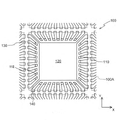
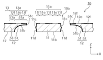
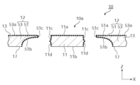
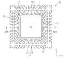
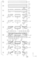
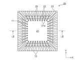
- FIG. 1 is a plan view showing the lead frame according to the first embodiment.
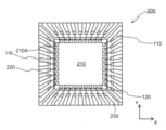
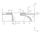
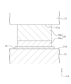
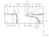
- FIG. FIG. 2 is a partially cut end view of the lead frame according to the first embodiment.
- FIG. 3 is a plan view showing the semiconductor device according to the first embodiment.
- FIG. 4 is a partially cut end view of the semiconductor device according to the first embodiment.
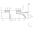
- FIG. 5 is a partially cut end view of a semiconductor device according to a modification of the first embodiment.
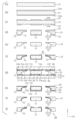
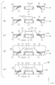
- FIG. 6A is a process diagram for explaining the method of manufacturing the lead frame according to the first embodiment.
- FIG. 6B is a process diagram following FIG. 6A for explaining the method of manufacturing the lead frame according to the first embodiment.
- FIG. 6C is a process drawing following FIG. 6B for explaining the method of manufacturing the lead frame according to the first embodiment.
- FIG. 6A is a process diagram for explaining the method of manufacturing the lead frame according to the first embodiment.
- FIG. 6B is a process diagram following FIG. 6A for explaining the method of manufacturing the lead frame according to the first
- FIG. 6D is a process drawing following FIG. 6C for explaining the method of manufacturing the lead frame according to the first embodiment.
- FIG. 6E is a process drawing following FIG. 6D for explaining the method of manufacturing the lead frame according to the first embodiment.
- FIG. 6F is a process drawing following FIG. 6E for explaining the method of manufacturing the lead frame according to the first embodiment.
- FIG. 6G is a process drawing following FIG. 6F for explaining the method of manufacturing the lead frame according to the first embodiment.
- FIG. 6H is a process drawing following FIG. 6G for explaining the method of manufacturing the lead frame according to the first embodiment.
- FIG. 7A is a process diagram for explaining the method of manufacturing the semiconductor device according to the first embodiment.
- FIG. 7B is a process drawing following FIG.
- FIG. 7A for explaining the method of manufacturing the semiconductor device according to the first embodiment.
- FIG. 7C is a process drawing following FIG. 7B for explaining the method of manufacturing the semiconductor device according to the first embodiment.
- FIG. 7D is a process drawing following FIG. 7C for explaining the method of manufacturing the semiconductor device according to the first embodiment.
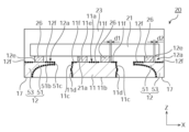
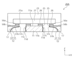
- FIG. 8 is a plan view showing the lead frame according to the second embodiment.
- FIG. 9 is a cross-sectional view (cross-sectional view taken along line IX-IX in FIG. 8) showing the lead frame according to the second embodiment.
- 10A and 10B are enlarged plan views showing the surface of the die pad and the surface of the lead, respectively.
- FIG. 11 is a plan view showing the semiconductor device according to the second embodiment.
- FIG. 12 is a cross-sectional view (cross-sectional view taken along line XII-XII in FIG. 11) showing the semiconductor device according to the second embodiment.
- 13(a) and 13(b) are enlarged cross-sectional views showing bumps as connection portions, respectively.
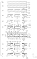
- 14(a)-(i) are cross-sectional views showing the method of manufacturing the lead frame according to the second embodiment.
- 15A to 15D are cross-sectional views showing the method of manufacturing the semiconductor device according to the second embodiment.
- FIG. 16 is a partially enlarged cross-sectional view showing the semiconductor device according to the second embodiment.
- FIGS. 17(a) to 17(d) are enlarged plan views respectively showing the surface of the die pad and the surface of the lead portion according to the modified example of the second embodiment.
- FIG. 18 is a plan view showing the lead frame according to the third embodiment.
- FIG. 19 is a cross-sectional view (cross-sectional view taken along line XIX-XIX in FIG. 18) showing the lead frame according to the third embodiment.
- FIG. 20 is a plan view showing the semiconductor device according to the third embodiment.
- FIG. 21 is a cross-sectional view (cross-sectional view taken along the line XXI-XXI of FIG. 20) showing the semiconductor device according to the third embodiment.
- FIG. 22 is an enlarged cross-sectional view showing a bump as a connecting portion.
- 23(a)-(i) are cross-sectional views showing the method of manufacturing the lead frame according to the third embodiment.
- FIG. 24A to 24D are cross-sectional views showing the method of manufacturing the semiconductor device according to the third embodiment.
- FIG. 25 is a partially enlarged cross-sectional view showing the semiconductor device according to the third embodiment.
- FIG. 26 is a cross-sectional view showing the lead frame according to the fourth embodiment.
- FIG. 27 is a cross-sectional view showing the semiconductor device according to the fourth embodiment.
- 28(a)-(j) are cross-sectional views showing the method of manufacturing the lead frame according to the fourth embodiment.
- FIG. 29 is a partially enlarged cross-sectional view showing the semiconductor device according to the fourth embodiment.
- FIG. 30 is a plan view showing a lead frame according to a fifth embodiment
- 31 is a cross-sectional view showing the lead frame according to the fifth embodiment (cross-sectional view taken along line XXXI-XXXI in FIG. 30)
- FIG. 32 is a plan view showing a semiconductor device according to a fifth embodiment
- FIG. 33 is a cross-sectional view showing the semiconductor device according to the fifth embodiment (cross-sectional view taken along line XXXIII-XXXIII in FIG. 32);
- FIG. 34 is an enlarged cross-sectional view showing a bump as a connecting portion;
- 35(a) to 35(j) are sectional views showing a method of manufacturing a lead frame according to the fifth embodiment;
- FIG. 36(a) to 36(d) are cross-sectional views showing the method of manufacturing the semiconductor device according to the fifth embodiment
- FIG. 37 is a partially enlarged cross-sectional view showing a semiconductor device according to a fifth embodiment
- FIG. 38 is a cross-sectional view showing a lead frame according to a sixth embodiment
- FIG. 39 is a cross-sectional view showing a semiconductor device according to a sixth embodiment
- 40(a) to 40(j) are cross-sectional views showing a method of manufacturing a lead frame according to the sixth embodiment
- 41 is a partially enlarged cross-sectional view showing a semiconductor device according to a sixth embodiment
- FIG. FIG. 42 is a cross-sectional view showing a lead frame according to a seventh embodiment
- FIG. 43 is a cross-sectional view showing a semiconductor device according to a seventh embodiment; 44(a) to 44(j) are cross-sectional views showing a method of manufacturing a lead frame according to the seventh embodiment;
- FIG. 45 is a partially enlarged cross-sectional view showing a semiconductor device according to a seventh embodiment;
- FIG. 46 is a cross-sectional view showing a lead frame according to an eighth embodiment;
- FIG. 47 is a cross-sectional view showing a semiconductor device according to an eighth embodiment;
- 48(a)-(j) are cross-sectional views showing a method of manufacturing a lead frame according to the eighth embodiment;
- FIG. 49 is a partially enlarged cross-sectional view showing a semiconductor device according to an eighth embodiment;
- FIG. 50 is a plan view showing a lead frame according to a ninth embodiment
- FIG. 51 is a cross-sectional view showing the lead frame according to the ninth embodiment (cross-sectional view taken along line LI-LI in FIG. 50)
- FIG. 52 is a plan view showing a semiconductor device according to a ninth embodiment
- FIG. 53 is a cross-sectional view (cross-sectional view taken along line LIII-LIII of FIG. 52) showing the semiconductor device according to the ninth embodiment
- 54(a) to 54(e) are sectional views showing a method of manufacturing a lead frame according to the ninth embodiment
- FIG. 55(a) to 55(h) are sectional views showing a method of manufacturing a lead frame according to the ninth embodiment
- FIG. 56(a) to 56(e) are cross-sectional views showing the method of manufacturing the semiconductor device according to the ninth embodiment
- FIG. 57 is a partially enlarged cross-sectional view showing a semiconductor device according to a ninth embodiment
- FIG. 58 is a cross-sectional view showing a lead frame according to a modification of the ninth embodiment
- a numerical range represented using “ ⁇ ” means a range that includes the numerical values described before and after “ ⁇ ” as lower and upper limits, respectively.
- terms such as “film”, “sheet”, and “plate” are not distinguished from each other based on the difference in designation.
- “plate” is a concept that includes members that can be generally called “sheets” and “films.”
- the lead frame 100 is used to manufacture a semiconductor device 200 (see FIGS. 3 and 4).
- the leadframe 100 has a plurality of package regions 100A.
- the plurality of package regions 100A are arranged in multiple rows and multiple stages (matrix). Note that FIG. 1 shows only a portion of the lead frame 100 centering on one package region 100A.
- the package area 100A is an area corresponding to a semiconductor device 200, which will be described later, and is an area surrounded by rectangular imaginary lines (broken lines shown in FIG. 1) (see FIG. 1).
- the lead frame 100 includes a plurality of package regions 100A, but the lead frame 100 is not limited to this embodiment, and the lead frame 100 is composed of only one package region 100A. may have been
- the terms “inner” and “inner” refer to the side toward the center of each package region 100A, and the terms “outer” and “outer” refer to the sides away from the center of each package region 100A. (Connecting bar 130 side).
- the “upper surface” refers to the surface on which the semiconductor element 210 is mounted
- the “lower surface” refers to the surface opposite to the “upper surface”, which is mounted on an external mounting substrate (not shown).
- the term “side wall surface” refers to the surface to be connected, and the “side wall surface” is a surface located between the “upper surface” and the “lower surface”, which constitutes the thickness of the lead frame 100 (metal substrate 310).
- half-etching means etching the material to be etched halfway in its thickness direction.
- the thickness of the material to be etched after half-etching is 30% to 70%, preferably 40% to 60%, of the thickness of the material to be etched before half-etching.
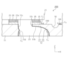
- each package region 100A of the lead frame 100 includes a plurality of lead portions 110, a die pad portion 120, and a connecting bar 130 connecting the lead portions 110.
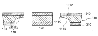
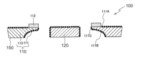
- Lead portion 110 may include inner lead portion 111 and terminal portion 113 .
- the inner lead portion 111 is a portion thinned from the lower surface side, and is positioned inside (on the die pad portion 120 side) in each package region 100A.
- the terminal portion 113 is positioned on the outside (connecting bar 130 side) in each package region 100A.
- the inner lead portion 111 extends from the terminal portion 113 toward the die pad portion 120 .
- An internal terminal is formed on the upper surface side of the inner lead portion 111 .
- the internal terminals are regions electrically connected to the semiconductor element 210 through the connecting members 220 as described later.
- a metal plating layer 112 is provided on the internal terminals to improve adhesion with the connection member 220 .
- Each lead portion 110 is connected to the semiconductor element 210 via a connection member 220 as will be described later, and is arranged with a space between it and the die pad portion 120 (see FIGS. 4 and 5). .
- the plurality of lead portions 110 are spaced apart from each other along the longitudinal direction of the connecting bar 130 .
- Each lead portion 110 extends from the connecting bar 130 respectively.
- the lead portion 110 is arranged along the periphery of the die pad portion 120 .
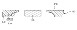
- the lead portion 110 is partially thinned from the lower surface side.
- the inner lead portion 111 is the portion that is thinned from the lower surface side.
- a portion of the lead portion 110 that is not thinned from the lower surface side is the terminal portion 113 , and the external terminal 150 is formed on the lower surface of the terminal portion 113 .
- the external terminal 150 is a portion electrically connected to an external mounting board (not shown).
- the external terminal 150 is a portion exposed to the outside of the semiconductor device 200, which will be described later.
- the inner lead portion 111 is thinned by, for example, half-etching from the lower surface side.
- the inner lead portion 111 has an inner lead portion upper surface 111A, an inner lead portion lower surface 111B facing the inner lead portion upper surface 111A, and an inner lead portion side wall surface.
- the inner lead portion upper surface 111A is a part of the upper surface of the lead portion 110 .
- the inner lead side wall surface includes a die pad portion facing surface 111C facing the die pad portion 120 side and a surface facing the adjacent lead portion 110 .
- the inner lead portion lower surface 111B is positioned below the lead portion 110 .
- the terminal portion 113 is located on the connecting bar 130 side. Terminal portion 113 is connected to connecting bar 130 .
- the lower surface of the terminal portion 113 constitutes the external terminal 150 described above.
- the terminal portion 113 has the same thickness as the die pad portion 120 without being half-etched. A portion of the lower surface of the terminal portion 113 located on the connecting bar 130 side may be thinned to form a connection portion with the connecting bar 130 .
- At least a part of the upper surface and side wall surfaces of the lead portions 110 are roughened surfaces, and the lower surfaces of the lead portions 110 (terminal portions 113) are non-roughened surfaces.
- the inner lead portion lower surface 111B is a roughened rough surface.
- the roughened rough surface is shown by the thick broken line.
- the rough surface when simply referred to as a "rough surface”, the rough surface means a rough surface that has been roughened, preferably a rough surface that has been roughened by microetching or the like.
- a thinned portion of the lower surface of the lead portion 110 is a roughened rough surface.
- the entire inner lead portion lower surface 111B is a rough surface.
- the portion of the lower surface of the lead portion 110 that is not thinned is a non-roughened surface.
- the terminal portion 113 is not thinned from the lower surface side, and the entire external terminal 150 located on the lower surface side of the terminal portion 113 has a non-roughened surface.
- the inner lead portion side wall surface including the die pad portion facing surface 111C is a rough surface in which the entire area is roughened.
- a part of the upper surface of the lead portion 110 (inner lead portion 111) located on the die pad portion 120 side may be a non-roughened surface, and the metal plating layer 112 is provided on the non-roughened surface.
- the metal plating layer 112 may be formed by electroplating, for example.
- the thickness of the metal plating layer 112 may be in the range of 1 ⁇ m to 10 ⁇ m.
- the metal plating layer 112 is, for example, Ag plating layer, Ag alloy plating layer, Au plating layer, Au alloy plating layer, Pt plating layer, Cu plating layer, Cu alloy plating layer, Pd plating layer, Ni plating layer, etc. It may well contain one or more of these.
- the metal plating layer 112 preferably includes at least one of an Ag plating layer, a Ni plating layer, a Pd plating layer, and an Au plating layer.
- a well-known base plating may be applied.
- a Ni plating layer, a Cu plating layer, or the like can be used as the base plating.
- a semiconductor element 210 is mounted on the upper surface of the die pad section 120 as described later. Moreover, it is sufficient that a plurality of lead portions 110 are arranged around the die pad portion 120 .
- the upper surface and side wall surfaces of the die pad section 120 may be roughened surfaces, and the lower surface of the die pad section 120 may be a non-roughened surface (see FIG. 2).
- the upper surface of the die pad portion 120 is a region (internal terminal) that is bonded to the semiconductor element 210 via an adhesive 240 such as die attach paste, as will be described later.
- the lower surface of the die pad portion 120 is not thinned by, for example, half-etching, and is a non-roughened surface that is not roughened like the metal substrate 310 before processing, which will be described later.
- a lower surface of the die pad portion 120 is exposed to the outside in a semiconductor device 200 which will be described later.
- the package regions 100A are connected to each other via connecting bars 130, and the connecting bars 130 extend along the X and Y directions.
- the X direction and the Y direction are two directions parallel to each side of the package region 100A in the plane of the lead frame 100, and the X direction and the Y direction are orthogonal to each other.
- Each connecting bar 130 is arranged around the package area 100A and outside the package area 100A.
- Each connecting bar 130 has an elongated rod shape in plan view.
- the width W of each connecting bar 130 (the distance in the direction perpendicular to the longitudinal direction of the connecting bar 130) is not particularly limited, but can be set appropriately within the range of 95 ⁇ m to 250 ⁇ m, for example.
- a plurality of lead portions 110 are connected to each connecting bar 130 at predetermined intervals along the longitudinal direction of the connecting bar 130 , and the die pad portion 120 is supported by the connecting bar 130 via suspension leads 140 . ing.
- the connecting bar 130 in this embodiment is not thinned, it is not limited to this aspect.
- the connecting bar 130 may be thinned by half-etching from its lower surface side.
- the thickness of the connecting bar 130 in this case can be set in consideration of the configuration of the semiconductor device 200 and the like.
- the thickness of the connecting bar 130 can be appropriately set within a range of, for example, 80 ⁇ m to 200
- the lead frame 100 is used to manufacture a semiconductor device 200 having a sealing portion 230 which will be described later.
- the sidewall surface may be a rough surface that is roughened.
- the upper surface of the lead portion 110, the side wall surface of the lead portion 110, and the connecting bar 130 located outside the package region 100A may be roughened surfaces, or may be non-roughened surfaces. It can be a face.
- the lead frame 100 is diced along the connecting bar 130 when the semiconductor device 200 is manufactured using the lead frame 100 . At this time, if each package region 100A is individually molded and diced, if the upper surface of the connecting bar 130 is roughened, there is a risk that foreign matter will be generated when the lead frame 100 is diced. Therefore, by forming the upper surface of the connecting bar 130 as a non-roughened surface, it is possible to suppress the generation of foreign matter when manufacturing the semiconductor device 200 .
- the a * value in the CIELab color space is in the range of 12 to 19
- the b * value is in the range of 12 to 17
- the a * value is preferably 13. ⁇ 18 with b * values in the range of 12-16.
- the surface area ratio increases. Become. Therefore, in a semiconductor device that can be manufactured using the lead frame 100, the adhesion strength with the mold resin increases. As a result, it is possible to prevent moisture in the air from entering the electrodes of the semiconductor element.
- the a * value and the b * value in the CIELab color space of the rough surface in the lead frame 100 according to the present embodiment are within the above range, thereby suppressing the infiltration of moisture in the air to the electrodes of the semiconductor element. possible semiconductor devices can be manufactured.
- the a * value and b * value in the CIELab color space are measured using a spectral density/colorimeter eXact (manufactured by X-rite).
- the CIELab color space (L * a * b * color space) will be described.
- the L * a * b * color space is the CIELab chromaticity diagram recommended by the CIE.
- L * represents lightness
- a * represents the degree of red/magenta or green
- b * represents the degree of yellow or blue.
- the more the value of b * goes to the minus side, the closer to blue, and the more to the plus side, the closer to yellow.
- An L * value of 100 indicates white (total reflection), and an L * value of 0 indicates black (total absorption).
- the center of these three values is the neutral color (gray). That is, movement along the L * axis indicates a change in lightness, and movement on the a * b * plane indicates a change in hue.
- the distance in the L * a * b * space corresponds to the closeness of colors, and it can be said that the closer the distance, the closer the color.
- the a * value in the CIELab color space is between red/magenta and green
- the b * value is between yellow and blue. can be said to be equivalent.
- the arithmetic mean curvature Spc of the peak point of the rough surface is 700 mm ⁇ 1 or more, preferably 1000 mm ⁇ 1 to 5000 mm ⁇ 1 , more preferably 2000 mm ⁇ 1 to 4000 mm -1 .
- the contact point with the contacted body is sharp. It is shown that.
- the adhesion strength with the mold resin is increased, and it is possible to suppress the infiltration of moisture in the air to the electrodes of the semiconductor element. That is, the arithmetic mean curvature Spc of the peak point of the rough surface in the lead frame 100 according to the present embodiment is within the above range, thereby manufacturing a semiconductor device capable of suppressing penetration of moisture in the air to the electrodes of the semiconductor element. can. Furthermore, the arithmetic mean height Sa of the rough surface is preferably 0.12 ⁇ m or more, more preferably in the range of 0.12 ⁇ m to 0.34 ⁇ m.
- the arithmetic mean curvature Spc of the peak points of the rough surface is 700 mm ⁇ 1 or more, and the arithmetic mean height Sa of the rough surface is within a predetermined range, so that moisture in the air can be effectively prevented from reaching the electrodes of the semiconductor element. It is possible to manufacture a semiconductor device that can be effectively suppressed.
- the arithmetic mean curvature Spc of the peak points represents the average of the principal curvatures of the peak points present in the object.
- the arithmetic mean height Sa is a parameter obtained by extending the arithmetic mean height Ra of lines to three dimensions, that is, a plane, and represents the average of the absolute values of the height differences of each point with respect to the average plane of the surface.
- the arithmetic mean curvature Spc and the arithmetic mean height Sa of the summit point are measured using a laser microscope VK-X260 (manufactured by Keyence Corporation, measurement section) and a laser microscope VK-X250 (manufactured by Keyence Corporation, controller section). measured using
- the inventors have found that the state of the roughened surface of the lead frame is important for the lead frame used in the semiconductor device.
- the inventors noticed that attention should be paid to the CIELab color space or the arithmetic mean curvature Spc and the arithmetic mean height Sa of the peak point as indices indicating the state of the rough surface.
- the rough surface according to the present embodiment may be formed, for example, by roughening the metal substrate 310 described later with a micro-etching liquid.
- the microetching liquid that can be used in the present embodiment includes those containing sulfuric acid or hydrochloric acid as main components, those containing hydrogen peroxide and sulfuric acid as main components, and the like.
- the rough surface in this embodiment has an a * value in the range of 12-19 and a b * value in the range of 12-17 in the CIELab color space. Further, the arithmetic mean curvature Spc of the peak points of the rough surface is 700 mm ⁇ 1 or more, and the arithmetic mean height Sa of the rough surface is 0.12 ⁇ m or more.
- the lead frame 100 described above is made of metal such as copper, copper alloy, or Ni alloy.
- the thickness of the lead frame 100 can be set in consideration of the configuration of the semiconductor device 200 and the like.
- the lead portions 110 in this embodiment are arranged along all four sides of the package region 100A, but are not limited to this. may be
- the portion 110 may be connected to the semiconductor element 210 via a bump as a connection member 220 as described later (see FIG. 5).
- the semiconductor device 200 includes a plurality of lead portions 110, a die pad portion 120, a semiconductor element 210, a connection member 220, and a sealing portion 230.
- FIG. 1 An embodiment of a semiconductor device of the present disclosure will be described.
- the semiconductor device 200 includes a plurality of lead portions 110, a die pad portion 120, a semiconductor element 210, a connection member 220, and a sealing portion 230.
- the semiconductor device 200 in this embodiment is manufactured using the lead frame 100 described above. Therefore, the lead portion 110 and the die pad portion 120 in the semiconductor device 200 are provided in the lead frame 100 described above. Therefore, the upper surface of the lead portion 110 outside the metal plating layer 112 (the side farther from the die pad portion 120) and the sidewall surface of the lead portion 110 are rough surfaces. In addition, the upper surface of the die pad portion 120 and the side wall surfaces of the die pad portion 120 are also rough surfaces.
- the lead portion 110 includes an inner lead portion 111 thinned from the lower surface side of the lead portion 110, and the inner lead portion lower surface 111B is a rough surface.
- a sealing portion 230 is in close contact with the lower surface 111B of the inner lead portion.
- the terminal portion 113 of the lead portion 110 is not thinned from the lower surface side.
- the external terminal 150 located on the lower surface of the terminal portion 113 has a non-roughened surface. The external terminals 150 are exposed from the sealing portion 230 .
- the rough surface has an a * value in the range of 12-19 and a b * value in the range of 12-17 in the CIELab color space.
- a * value and b * value in the CIELab color space of the rough surface are within the above range, it is possible to suppress the infiltration of moisture in the air to the electrodes of the semiconductor element 210 .
- the arithmetic mean curvature Spc of the peak point of the rough surface is 700 mm ⁇ 1 or more.
- the arithmetic mean height Sa of the rough surface is preferably 0.12 ⁇ m or more, more preferably in the range of 0.12 ⁇ m to 0.34 ⁇ m.
- the arithmetic mean curvature Spc of the peak points of the rough surface is 700 mm ⁇ 1 or more, and the arithmetic mean height Sa of the rough surface is within a predetermined range. can be suppressed more effectively.
- the semiconductor element 210 can use various semiconductor elements commonly used in the past, and is not particularly limited. For example, integrated circuits, large-scale integrated circuits, transistors, thyristors, diodes, etc. can be used. can be done.
- This semiconductor element 210 has a plurality of electrodes 210A to which connecting members 220 are attached.
- connection member 220 is made of, for example, a highly conductive metal material such as copper or gold. They are electrically connected to the metal plating layers 112 respectively. It should be noted that conductors such as bonding wires and bumps may be used as the connection member 220 .
- the sealing portion 230 seals at least the lead portion 110 , the die pad portion 120 , the semiconductor element 210 and the connection member 220 .
- the sealing portion 230 may be made of, for example, thermosetting resin such as silicone resin or epoxy resin; thermoplastic resin such as PPS resin.
- the thickness of the entire sealing portion 230 is not particularly limited, but can be appropriately set within a range of, for example, approximately 300 ⁇ m to 1500 ⁇ m.
- the length of one side of the sealing portion 230 is not particularly limited, but is appropriately set within a range of about 0.2 mm to 20 mm, for example. can be
- the portion 110 may be connected to the electrode 210A of the semiconductor element 210 via a bump as the connecting member 220 (see FIG. 5).
- FIGS. 1 and 2 A method for manufacturing the lead frame 100 shown in FIGS. 1 and 2 will be described as an example.
- 6A to 6H are process diagrams for explaining the method of manufacturing the lead frame according to this embodiment.
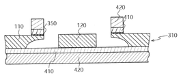
- a metal substrate 310 having a first surface 310A and a second surface 310B facing the first surface 310A is prepared (see FIG. 6A).
- the metal substrate 310 that can be used in this embodiment includes a pure copper substrate, a copper alloy substrate, a 42 alloy (Fe alloy with Ni of 42%) substrate, etc., but a pure copper substrate or a copper alloy substrate is preferable. Also, the metal substrate 310 may be used after the first surface 310A and the second surface 310B are degreased and cleaned.
- a photosensitive resist 320 is applied to each of the first surface 310A and the second surface 310B of the metal substrate 310 and dried (see FIG. 6B).
- a conventionally known one can be used as the photosensitive resist 320 that can be used in this embodiment.
- the metal substrate 310 is exposed through a photomask and developed to form a resist layer 340 having desired openings 330 (see FIG. 6C).
- the metal substrate 310 is etched with an etchant (see FIG. 6D).
- the etchant can be appropriately selected according to the material of the metal substrate 310 to be used. For example, when a pure copper substrate is used as the metal substrate 310, an aqueous solution of ferric chloride may be used as the etchant, and both the first surface 310A and the second surface 310B of the metal substrate 310 may be spray-etched. Thus, the outer shapes of the lead part 110, the die pad part 120 and the connecting bar 130 are formed. At this time, the inner lead portion 111 and the terminal portion 113 may be formed by partially thinning the lower surface of the lead portion 110 by half-etching.
- the resist layer 340 is peeled off, and a coating layer 350 is formed on the etched surface of the metal substrate 310 (see FIG. 6E).
- the coating layer 350 is formed all around the lead portion 110 , the die pad portion 120 and the connecting bar 130 .
- the thickness of the coating layer 350 is not particularly limited, but may be, for example, more than 0 ⁇ m and less than or equal to 2 ⁇ m.
- the metal forming the coating layer 350 is not particularly limited, but silver, for example, may be used.
- a silver plating solution containing silver cyanide and potassium cyanide as main components can be used as the plating solution for electroplating.
- the coating layer 350 may be formed on the lower surface of the external terminal 150 on the lower surface of the lead portion 110 (terminal portion 113 ) and the lower surface of the die pad portion 120 .
- the external terminal 150 on the lower surface of the lead portion 110 (terminal portion 113) and the The formation of the coating layer 350 may be avoided by forming the resist layer 400 on the lower surface of the die pad section 120 (see FIG. 6E).
- the covering layer 350 existing in the region where the rough surface is to be formed is removed. Specifically, the upper surface of the lead portion 110 other than the region where the metal plating layer 112 is provided, the side wall surface of the lead portion 110, the lower surface of the inner lead portion 111, the upper surface of the die pad portion 120, and the side wall surface of the die pad portion 120.
- the covering layer 350 formed on is removed (see FIG. 6F).
- elastic members 410 such as rubber packing are placed on the first surface 310A and the second surface 310B of the metal substrate 310, respectively, and the metal substrate 310 is sandwiched by jigs 420 via the elastic members 410. .
- the portion of the covering layer 350 that is not covered with the elastic member 410 is peeled off.
- the upper surface of the lead portion 110 other than the region where the metal plating layer 112 is provided, the side wall surface of the lead portion 110, the lower surface of the inner lead portion 111, the upper surface of the die pad portion 120, and the side wall surface of the die pad portion 120 are exposed. do.
- the top surface of the area where the metal plating layer 112 is formed on the top surface of the lead part 110 covered with the elastic member 410 and the coating layer 350 on the connecting bar 130 remain.
- a support layer 360 that supports the metal substrate is provided on the lower surface side of the metal substrate 310 (see FIG. 6G).
- Support layer 360 may be, for example, a resist layer.
- a rough surface is formed by roughening the portion of the metal substrate 310 that is not covered with the coating layer 350 (see FIG. 6G).
- the upper surface of the lead portion 110 outside the region where the metal plating layer 112 is formed the side farther from the die pad portion 120
- the side wall surface of the lead portion 110, the lower surface of the inner lead portion 111, the die pad A rough surface is formed on the upper surface of the portion 120 and the sidewall surface of the die pad portion 120 .
- a micro-etchant is supplied to the metal substrate 310 .
- a rough surface can be formed on the entire metal substrate 310 except for the portion covered with the coating layer 350 .
- the micro-etching liquid is a surface treatment agent capable of slightly dissolving the metal surface and forming a rough surface with fine unevenness.
- Examples of microetching solutions that can be used in the present embodiment include those containing sulfuric acid or hydrochloric acid as main components, those containing hydrogen peroxide and sulfuric acid as main components, and the like.
- the rough surface is roughened so that the a * value in the CIELab color space is in the range of 12-19 and the b * value is in the range of 12-17. Further, in the step of forming the rough surface, the rough surface is roughened so that the arithmetic mean curvature Spc of the crest point of the rough surface is 700 mm ⁇ 1 or more. Furthermore, the arithmetic mean height Sa of the rough surface is preferably 0.12 ⁇ m or more, more preferably in the range of 0.12 ⁇ m to 0.34 ⁇ m.
- the support layer 360 and the coating layer 350 are sequentially peeled off, and the metal plating layer 112 is provided on the inner (die pad 120 side) end of the upper surface 111A of the inner lead portion, thereby forming the lead frame shown in FIGS. 100 is obtained (see FIG. 6H).
- the metal plating layer 112 for example, a plating resist layer having a predetermined pattern is formed by photolithography, and the metal plating layer 112 can be formed by electroplating in areas not covered by the plating resist layer.
- the lead frame 100 manufactured by the manufacturing method described above may be subjected to alkali treatment. Specifically, the lead frame 100 is immersed in an alkaline aqueous solution.
- the acid contained in the surface treatment agent used in the rough surface forming step is neutralized, and corrosion of the lead frame 100 can be suppressed.
- the alkali used in the alkali treatment is not particularly limited, and examples thereof include sodium hydroxide, potassium hydroxide, etc., and one of these may be used alone, or two alkalis may be used. More than one species may be mixed and used.
- FIGS. 3 and 4 A method for manufacturing the semiconductor device 200 shown in FIGS. 3 and 4 will be described as an example.
- 7A to 7D are process diagrams for explaining the method of manufacturing the semiconductor device according to this embodiment.
- the lead frame 100 manufactured by the manufacturing method shown in FIGS. 6A to 6H is prepared (see FIG. 7A).
- the semiconductor element 210 is mounted on the die pad portion 120 of the lead frame 100 .
- the semiconductor element 210 is placed and fixed on the die pad section 120 using an adhesive 240 such as die attach paste (see FIG. 7B).
- the adhesive 240 may be an epoxy resin-based adhesive containing components such as silver paste and epoxy resin.
- the semiconductor element 210 is placed on the rough upper surface of the die pad portion 120 with the adhesive 240 interposed therebetween.
- each electrode 210A of the semiconductor element 210 and the metal plating layer 112 formed on each lead portion 110 are electrically connected to each other by connecting members 220 (see FIG. 7C).
- a sealing portion 230 is formed by injection molding or transfer molding a thermosetting resin or thermoplastic resin to the lead frame 100 (see FIG. 7D).
- the lead portion 110, the die pad portion 120, the semiconductor element 210, and the connection member 220 can be resin-sealed.
- the lead frame 100 is diced for each package area 100A.
- the upper surface of the connecting bar 130 to be diced is a non-roughened surface, it is possible to suppress the generation of foreign matter during dicing.
- the semiconductor devices 200 are separated into individual pieces, and the semiconductor devices 200 shown in FIGS. 3 and 4 are obtained.
- moisture in the air may enter from the side or bottom side of the semiconductor device 200 .
- moisture in the air may enter through the interface between the sealing portion 230 and the lead portion 110 or the die pad portion 120 .
- the upper surface of the lead portion 110 not provided with the metal plating layer 112, the side wall surface of the lead portion 110, the upper surface of the die pad portion 120, and the side wall surface of the die pad portion 120 are roughened. formed.
- the rough surface has an a * value in the range of 12 to 19 and a b * value in the range of 12 to 17 in the CIELab color space of the rough surface, or the arithmetic mean curvature of the crest points of the rough surface. It is roughened so that Spc is 700 mm ⁇ 1 or more and the arithmetic mean height Sa of the rough surface is 0.12 ⁇ m or more.
- the distance of the infiltration path through which moisture infiltrates from the interface between the sealing portion 230 and the lead portion 110 or the die pad portion 120 to the semiconductor element 210 side is relatively long. Therefore, it is possible to prevent moisture from entering the electrode 210A of the semiconductor element 210.
- FIG. Furthermore, by having the rough surface within the predetermined range, the adhesion strength between the die pad portion 120 or the lead portion 110 and the sealing portion 230 can be increased, and the die pad portion 120 or the lead portion 110 and the sealing portion 230 can be Peeling can be suppressed.
- the lead portion 110 in this embodiment includes an inner lead portion 111 thinned from the lower surface side of the lead portion 110 . Since the lower surface of the inner lead portion 111 is a rough surface, the distance of the path of entry of moisture at the interface between the sealing portion 230 and the lead portion 110 on the lower surface side of the semiconductor device 200 is long. This can prevent moisture from entering from the interface between the sealing portion 230 and the lead portion 110 to the electrodes 210A of the semiconductor element 210 . Furthermore, by providing the lower surface of the inner lead portion 111 with a rough surface within the predetermined range, the adhesion strength between the lead portion 110 and the sealing portion 230 can be increased, and the lead portion 110 and the sealing portion 230 are separated from each other. can be suppressed.
- Example 1 It has the configuration shown in FIGS.
- a lead frame 100 was prepared.
- the top surface and side wall surfaces of the lead portion 110 and the top surface and side wall surfaces of the die pad portion 120 have an a * value of 17.53 and a b * value of 14.80 in the CIELab color space. It was composed of a rough surface with an arithmetic mean curvature Spc of 2431.46 mm ⁇ 1 and an arithmetic mean height Sa of 0.14 ⁇ m.
- the a * value and b * value were measured using a spectral density/colorimeter eXact (manufactured by X-rite).
- X260 manufactured by Keyence Corporation, measurement section
- laser microscope VK-X250 manufactured by Keyence Corporation, controller section
- Example 2 The top surface and side wall surfaces of the lead portion 110 and the top surface and side wall surfaces of the die pad portion 120 have an a * value of 16.03, a b * value of 13.84, and an arithmetic mean curvature Spc of the peak point in the CIELab color space.
- a lead frame 100 having the same structure as in Example 1 was prepared, except that the rough surface had a surface roughness of 2952.08 mm ⁇ 1 and an arithmetic mean height Sa of 0.17 ⁇ m.
- Example 3 The top surface and side wall surfaces of the lead portion 110 and the top surface and side wall surfaces of the die pad portion 120 have an a * value of 15.39, a b * value of 13.16, and an arithmetic mean curvature Spc of the peak point in the CIELab color space.
- a lead frame 100 having the same structure as in Example 1 was prepared, except that the rough surface had a surface roughness of 3523.76 mm ⁇ 1 and an arithmetic mean height Sa of 0.22 ⁇ m.
- Example 4 The top surface and side wall surfaces of the lead portion 110 and the top surface and side wall surfaces of the die pad portion 120 have an a * value of 14.65, a b * value of 12.86, and an arithmetic mean curvature Spc of the peak point in the CIELab color space.
- a lead frame 100 having the same structure as in Example 1 was prepared, except that the rough surface had a surface roughness of 3378.00 mm ⁇ 1 and an arithmetic mean height Sa of 0.21 ⁇ m.
- the top surface and side wall surfaces of the lead portion 110 and the top surface and side wall surfaces of the die pad portion 120 have an a * value of 18.59, a b * value of 17.29, and an arithmetic mean curvature Spc of the peak point in the CIELab color space.
- a lead frame having the same structure as in Example 1 was prepared, except that the surface roughness was 629.05 mm ⁇ 1 and the arithmetic mean height Sa was 0.11 ⁇ m.
- the top surface and side wall surfaces of the lead portion 110 and the top surface and side wall surfaces of the die pad portion 120 have an a * value of 10.06, a b * value of 7.18, and an arithmetic mean curvature Spc of the peak point in the CIELab color space.
- a lead frame was prepared having the same configuration as in Example 1 , except that it was composed of a non-roughened surface with a surface roughness of 986.96 mm ⁇ 1 and an arithmetic mean height Sa of 0.09 ⁇ m.
- the molded resin had a height of 4 mm, a bottom diameter of 4 mm, and a top diameter of 3 mm, and the bottom side was molded into a lead frame.
- the lead frame was fixed to a bonding strength tester DAGE4000 (manufactured by Nordson), and the shear strength was measured by applying a shear load of 1 kg and a load of 0.1 mm/sec from the lateral direction of the mold resin on the lead frame. It was measured.
- the shear strength increases compared to when the arithmetic mean curvature Spc of the peak points is less than 700 mm ⁇ 1 . was confirmed. Furthermore, the arithmetic average height Sa of the rough surface of each of the lead frames 100 of Examples 1 to 4 was 0.12 ⁇ m or more.
- the arithmetic mean curvature Spc of the peak point of the rough surface is 700 mm ⁇ 1 or more, and the arithmetic mean height Sa of the rough surface is 0.12 ⁇ m or more, so that the semiconductor manufactured using the lead frame 100 In the device, the adhesion strength with the mold resin is increased, and it is presumed that the infiltration of moisture in the air to the electrodes 210A of the semiconductor element 210 can be suppressed.
- the arithmetic mean curvature Spc of the peak point of the non-roughened surface of Comparative Example 2 is 700 mm ⁇ 1 or more.
- the rough surface of the lead frames 100 of Examples 1 to 4 is rougher than the rough surface of the lead frame of Comparative Example 1.
- FIG. For this reason, it is presumed that the value of the arithmetic mean curvature Spc at the peak point was increased due to the deep etching.
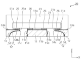
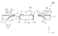
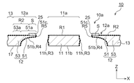
- FIG. 8 to 10 are diagrams showing the lead frame according to this embodiment.
- the lead frame 10 shown in FIGS. 8 and 9 is used when manufacturing the semiconductor device 20 (FIGS. 11 and 12).
- Such a lead frame 10 has a plurality of package regions 10a.
- the plurality of package regions 10a are arranged in multiple rows and multiple stages (in a matrix). Note that FIG. 8 shows only a portion of the lead frame 10 centering on one package region 10a.
- the terms “inside” and “inside” refer to the side facing the center of each package area 10a. “Outside” and “outside” refer to the side away from the center of each package region 10a (connecting bar 13 side).
- the “surface” refers to the surface on which the semiconductor element 21 is mounted.
- the “back surface” refers to the surface opposite to the “front surface” and connected to an external mounting board (not shown).
- “Side surface” refers to a surface located between the “front surface” and the “back surface” and constituting the thickness of the lead frame 10 (metal substrate).
- half-etching means etching the material to be etched halfway in its thickness direction.
- the thickness of the material to be etched after half-etching is, for example, 30% or more and 70% or less, preferably 40% or more and 60% or less of the thickness of the material to be etched before half-etching.
- each package region 10a of the lead frame 10 includes a die pad 11 and lead portions 12 positioned around the die pad 11. As shown in FIGS. Among them, the lead portion 12 is partly thinned from the back surface side. The thinned portion of the back surface of the lead portion 12 is a rough surface. A portion of the back surface of the lead portion 12 that is not thinned is a smooth surface.
- the package area 10a is an area corresponding to the semiconductor device 20 (described later).
- the package area 10a is an area surrounded by a rectangular imaginary line (two-dot chain line) in FIG.
- the lead frame 10 includes a plurality of package regions 10a.
- the present invention is not limited to this, and one lead frame 10 may be formed with only one package region 10a.
- the package regions 10a are connected to each other via a connecting bar (support member) 13.
- This connecting bar 13 supports the die pad 11 and the lead portion 12 .
- the connecting bar 13 extends along the X direction or the Y direction, respectively.
- the X direction and the Y direction are two directions parallel to each side of the package region 10 a within the plane of the lead frame 10 .
- the X direction and the Y direction are orthogonal to each other.
- the Z direction is a direction perpendicular to both the X direction and the Y direction.
- Each connecting bar 13 is arranged around the package area 10a and outside the package area 10a.
- Each connecting bar 13 has an elongated rod shape in plan view.
- the width of each connecting bar 13 (the distance in the direction orthogonal to the longitudinal direction of the connecting bar 13) may be 95 ⁇ m or more and 250 ⁇ m or less.
- a plurality of lead portions 12 are connected to each connecting bar 13 at intervals along the longitudinal direction of the connecting bar 13 .
- the die pad 11 is supported by the connecting bar 13 via suspension leads 14 .
- the connecting bar 13 is not thinned, it is not limited to this, and may be thinned by, for example, half-etching from the back side.
- the thickness of the connecting bar 13 may be 80 ⁇ m or more and 200 ⁇ m or less, depending on the configuration of the semiconductor device 20 .
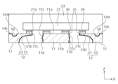
- the die pad 11 has a die pad front surface 11a located on the front side and a die pad back surface 11b located on the back side.
- a semiconductor element 21 is mounted on the die pad surface 11a as described later.
- the die pad back surface 11b is exposed to the outside from the semiconductor device 20 (described later).
- a first die pad side surface 11 c and a second die pad side surface 11 d are formed on the side of the die pad 11 facing the lead portion 12 .
- the first die pad side surface 11c is positioned on the die pad surface 11a side.
- the second die pad side surface 11d is located on the die pad back surface 11b side.
- the first die pad side surface 11c and the second die pad side surface 11d of the die pad 11 are rough surfaces.
- a smooth surface (die pad smooth surface region 11e) and a rough surface (die pad rough surface region 11f) are formed on the die pad surface 11a, as will be described later.
- the die pad back surface 11b is a smooth surface.
- the term "rough surface” refers to a surface having an S-ratio of 1.30 or more.
- a “smooth surface” refers to a surface having an S-ratio of less than 1.30.
- a rough surface is a surface that is rougher than a smooth surface.
- the S-ratio of the "rough surface” is preferably 1.30 or more and 2.30 or less.
- the S-ratio of the "smooth surface” is preferably 1.00 or more and 1.20 or less.
- the "S-ratio" is obtained by dividing the surface area obtained by dividing the surface to be measured into a plurality of pixels with an optical interferometer and measuring it by the observed area. Specifically, the surface to be measured is divided into a plurality of pixels using a VertScan manufactured by Hitachi High-Tech Science Co., Ltd., and the obtained surface area is divided by the observation area for calculation.
- the roughened surface may be formed by subjecting the outer surface of the metal substrate 31, which will be described later, to a roughening treatment with a micro-etching liquid containing, for example, hydrogen peroxide and sulfuric acid as main components.
- the smooth surface may be an unprocessed surface on which the metal substrate 31, which will be described later, is not subjected to such roughening treatment.
- the roughened portion is indicated by a thick dashed line (the same applies to other cross-sectional views).
- the die pad surface 11a of the die pad 11 is a region (internal terminal) that is electrically connected to the semiconductor element 21 via the bumps 26, as will be described later.
- the die pad surface 11a may be a region that is not thinned by half-etching or the like.
- a die pad smooth surface region 11e, which is a smooth surface region, and a die pad rough surface region 11f, which is a rough surface region, are formed on the die pad surface 11a.
- a plurality of die pad smooth surface regions 11e may be formed on the die pad surface 11a.
- the die pad smooth surface regions 11e are connected to corresponding bumps 26 (see FIG. 12).
- the number of die pad smooth surface regions 11e on the die pad 11 and the number of bumps 26 connected to the die pad 11 may be the same.
- a plurality of bumps 26 may be arranged in one die pad smooth surface region 11e. In this case, the number of die pad smooth surface regions 11 e on the die pad 11 may be less than the number of bumps 26 connected to the die pad 11 .
- the die pad rough surface region 11f is rougher (larger S-ratio) than the die pad smooth surface region 11e. As shown in FIG. 10A, the die pad rough surface region 11f is formed so as to surround the entire periphery of each die pad smooth surface region 11e in plan view. That is, the die pad smooth surface region 11 e does not come into direct contact with the peripheral edge 11 g of the die pad 11 .
- the die pad rough surface region 11f is formed along the entire peripheral edge 11g of the die pad 11 in plan view.
- the peripheral edge 11g of the die pad 11 refers to a region surrounded by a plurality of (four) sides of the die pad 11, as shown in FIG.
- the die pad surface 11a may be formed entirely of the die pad rough surface region 11f except for the die pad smooth surface region 11e. That is, the die pad surface 11a may be composed only of a plurality of die pad smooth surface regions 11e and other die pad rough surface regions 11f.
- the die pad smooth surface region 11e may be circular in plan view.
- the die pad smooth surface region 11e is preferably larger than the bump 26 (phantom line) in plan view.
- the width (diameter) D1 of the die pad smooth surface region 11e may be 0.030 mm or more, or may be 0.035 mm or more.
- the width (diameter) D1 may be 0.070 mm or less, or may be 0.065 mm or less.
- the shortest distance d1 between the periphery of the bumps 26 and the periphery of the die pad smooth surface region 11e may be 0.005 mm or more, or 0.010 mm or more.
- the shortest distance d1 may be 0.020 mm or less, or 0.015 mm or less.
- the shortest distance L1 between the die pad smooth surface region 11e and the peripheral edge 11g of the die pad 11 may be 0.025 mm or more, or may be 0.030 mm or more.
- the shortest distance L1 may be 1.0 mm or less, or may be 0.50 mm or less.
- the circular bumps 26 can be easily positioned with respect to the die pad smooth surface region 11e.
- smooth surface portions are shown in white, and rough surface portions are shaded (the same applies to FIGS. 17(a) to (d)).
- the shortest distance M1 between adjacent die pad smooth surface regions 11e may be 0.030 mm or more, or 0.040 mm.
- the above may be used.
- the shortest distance M1 may be 1.0 mm or less, or may be 0.50 mm or less.
- the pitch P1 between the centers of the die pad smooth surface regions 11e adjacent to each other may be 0.045 mm or more, or may be 0.057 mm or more.
- the pitch P1 may be 1.2 mm or less, or may be 0.60 mm or less.
- the pitch P1 corresponds to the pitch between the centers of the bumps 26 adjacent to each other.
- the die pad back surface 11b of the die pad 11 may be formed with external terminals. This external terminal may be electrically connected to a mounting board (not shown).
- the die pad back surface 11b is not thinned by, for example, half-etching, and is a smooth surface similar to the metal substrate (metal substrate 31 described later) before processing.
- the die pad back surface 11b is exposed to the outside from the semiconductor device 20 after manufacturing the semiconductor device 20 (described later).
- Each lead portion 12 is connected to the semiconductor element 21 through a bump 26 as will be described later, and is arranged with a space between it and the die pad 11 .
- the plurality of lead portions 12 are arranged at intervals along the longitudinal direction of the connecting bar 13 .
- Each lead portion 12 extends from the connecting bar 13 respectively.
- the lead portion 12 is arranged along the periphery of the die pad 11 .
- a portion of the lead portion 12 is thinned from the rear surface side.
- the back surface of the inner lead 51, which will be described later, of the lead portion 12 is thinned.
- An external terminal 17 is formed on the portion of the back surface of the lead portion 12 that is not thinned.
- the external terminals 17 are electrically connected to an external mounting board (not shown).
- the external terminals 17 are exposed to the outside from the semiconductor device 20 after manufacturing the semiconductor device 20 (described later).
- the lead portion 12 has inner leads 51 and terminal portions 53 .
- the inner lead 51 is located inside (on the die pad 11 side).
- the terminal portion 53 is positioned on the outside (connecting bar 13 side).
- the inner lead 51 extends from the terminal portion 53 to the die pad 11 side.
- An internal terminal is formed on the surface side of the inner lead 51 .
- This internal terminal is a region (lead smooth surface region 12e) electrically connected to the semiconductor element 21 via the bump 26, as will be described later.
- the inner lead 51 is thinned by, for example, half-etching from the back side.
- the inner lead 51 has an inner lead surface 51a and an inner lead back surface 51b.
- the inner lead surface 51a is located on the surface side.
- An inner lead tip surface 51c is formed on a surface of the inner lead 51 facing the die pad 11. As shown in FIG.
- the inner lead back surface 51b is located on the back surface side.
- the terminal portion 53 is located on the connecting bar 13 side. A proximal end portion of the terminal portion 53 is connected to the connecting bar 13 .
- the terminal portion 53 has a terminal portion surface 53a.
- the external terminals 17 described above are formed on the rear surface of the terminal portion 53 .
- the terminal portion 53 has the same thickness as the die pad 11 without being half-etched. It should be noted that the back surface of the portion of the lead portion 12 positioned closer to the connecting bar 13 than the terminal portion 53 may be thinned to form a connection portion with the connecting bar 13 .
- the thinned portion of the back surface of the lead portion 12 is a rough surface.
- the inner lead 51 of the lead portion 12 is thinned from the back side.
- An inner lead rear surface 51b positioned on the rear surface side of the inner lead 51 is roughened over its entire area.
- the portion of the back surface of the lead portion 12 that is not thinned is a smooth surface.
- the terminal portion 53 of the lead portion 12 is not thinned from the back side.
- the external terminals 17 located on the rear surface side of the terminal portion 53 have a smooth surface over the entire area.
- the entire inner lead tip surface 51c of the lead portion 12 is roughened. Moreover, although not shown, both side surfaces along the longitudinal direction of the lead portion 12 may be roughened. On the other hand, the inner lead 51 of the lead portion 12 is not thinned from the surface side. Also, the terminal portion 53 of the lead portion 12 is not thinned from the surface side.
- the inner lead surface 51a of the inner lead 51 and the terminal portion surface 53a of the terminal portion 53 constitute the lead surface 12a.
- the lead surface 12a is a region that has not been thinned from the surface side by half-etching or the like.
- a lead smooth surface region 12e, which is a smooth surface region, and a lead rough surface region 12f, which is a rough surface region, are formed on the lead surface 12a.
- each lead portion 12 is formed with one lead smooth surface region 12e.
- a plurality of lead smooth surface regions 12e may be formed on the lead surface 12a of each lead portion 12, respectively.
- the lead smooth surface regions 12e are connected to corresponding bumps 26 (see FIG. 12).
- a plurality of bumps 26 may be arranged in one lead smooth surface region 12e. In this case, the number of lead smooth surface regions 12 e on each lead portion 12 may be less than the number of bumps 26 connected to the lead portion 12 .
- a lead rough surface region 12f exists around the lead smooth surface region 12e.
- the lead rough surface region 12f is rougher (larger S-ratio) than the lead smooth surface region 12e.
- the lead rough surface region 12f is formed so as to surround the entire periphery of each lead smooth surface region 12e in plan view. That is, the lead smooth surface region 12e does not come into direct contact with the peripheral edge 12g of the lead portion 12.
- the lead rough surface region 12f is formed along the entire peripheral edge 12g of the lead portion 12 in plan view.
- the peripheral edge 12g of the lead portion 12 refers to a region surrounded by a plurality (three) sides of the lead portion 12 and the connecting bar 13, as shown in FIG.
- all the lead surface 12a other than the lead smooth surface region 12e may be the lead rough surface region 12f. That is, the lead surface 12a may be composed only of the lead smooth surface region 12e and the other lead rough surface region 12f.
- the lead smooth surface region 12e may be circular in plan view.
- the shape of the lead smooth surface region 12e may be the same as or different from that of the die pad smooth surface region 11e described above.
- the lead smooth surface region 12e is preferably larger than the bump 26 (phantom line) in plan view.
- the width (diameter) D2 of the lead smooth surface region 12e may be 0.030 mm or more, or may be 0.035 mm or more.
- the width (diameter) D2 may be 0.070 mm or less, or may be 0.065 mm or less.
- the shortest distance d2 between the periphery of the bump 26 and the periphery of the lead smooth surface region 12e may be 0.005 mm or more, or 0.010 mm or more.
- the shortest distance d2 may be 0.020 mm or less, or 0.015 mm or less.
- the shortest distance L2 between the lead smooth surface region 12e and the peripheral edge 12g of the lead portion 12 may be 0.025 mm or more, or may be 0.030 mm or more.
- the shortest distance L2 may be 1.0 mm or less, or 0.50 mm or less. Since the lead smooth surface region 12e is circular in plan view, the circular bump 26 can be easily positioned with respect to the die pad smooth surface region 11e.
- the lead frame 10 described above is made of metal such as copper, copper alloy, 42 alloy (Ni 42% Fe alloy) as a whole.
- the thickness of the non-thinned portion of the lead frame 10 may be 80 ⁇ m or more and 300 ⁇ m or less, depending on the configuration of the semiconductor device 20 to be manufactured.
- the lead portions 12 are arranged along all four sides of the package region 10a, but the present invention is not limited to this. It's okay to be.
- FIG. 11 to 13 are diagrams showing the semiconductor device (flip chip type) according to this embodiment.
- a semiconductor device (semiconductor package) 20 includes a die pad 11, a semiconductor element 21, a plurality of lead portions 12, a plurality of bumps 26, and a sealing resin 23. .
- the semiconductor element 21 is mounted on the die pad 11 and the lead portion 12 .
- the plurality of bumps 26 electrically connect the semiconductor element 21 and the die pad 11 or the lead portion 12 respectively.
- the bumps 26 constitute connections.
- Bumps 26 may also be pillars.
- the encapsulating resin 23 encapsulates the die pad 11 , the lead portion 12 , the semiconductor element 21 and the bumps 26 .
- the die pad 11 and the lead portion 12 are produced from the lead frame 10 described above.
- the inner lead 51 of the lead portion 12 is thinned from the back side.
- the inner lead rear surface 51b of the inner lead 51 is roughened.
- the sealing resin 23 is in close contact with the back surface 51b of the inner lead.
- the terminal portion 53 of the lead portion 12 is not thinned from the back side.
- the external terminals 17 positioned on the rear surface of the terminal portion 53 have a smooth surface. The external terminals 17 are exposed outward from the sealing resin 23 .
- a bump 26 is provided on each of the die pad 11 and the lead portion 12 .
- the bumps 26 on the die pad 11 are provided in the die pad smooth surface region 11e.
- the bump 26 is spaced apart from the die pad rough surface region 11f by the shortest distance d1.
- the bump 26 on the lead portion 12 is provided on the lead smooth surface region 12e.
- the bump 26 is spaced apart from the lead rough surface region 12f by the shortest distance d2.
- the semiconductor element 21 , the die pad 11 and the lead portions 12 are electrically connected to each other through the bumps 26 .
- This semiconductor element 21 it is possible to use various semiconductor elements that have been generally used in the past, and there is no particular limitation, but for example, integrated circuits, large-scale integrated circuits, transistors, thyristors, diodes, etc. can be used.
- This semiconductor element 21 has a plurality of electrodes 21a to which bumps 26 are attached respectively.
- the sealing resin 23 a thermosetting resin such as silicone resin or epoxy resin, or a thermoplastic resin such as PPS resin can be used.
- the thickness of the entire sealing resin 23 may be about 300 ⁇ m or more and 1500 ⁇ m or less.
- One side of the sealing resin 23 (one side of the semiconductor device 20) may be, for example, 0.2 mm or more and 20 mm or less, or may be 0.2 mm or more and 16 mm or less. In FIG. 11, the portion of the sealing resin 23 located closer to the surface than the lead portions 12 and the semiconductor element 21 is omitted.
- the bump (connection part) 26 is made of a highly conductive metal material such as copper, and may have a substantially cylindrical or spherical solid shape.
- the bumps 26 have their upper ends connected to the electrodes 21a of the semiconductor element 21, and their lower ends connected to the die pad smooth surface region 11e or the lead smooth surface region 12e.
- the width (diameter) of the bump 26 may be 0.01 mm or more and 0.070 mm or less.
- the die pad 11 does not necessarily have to be provided with the bumps 26 . In this case, the die pad 11 and the semiconductor element 21 may be fixed to each other with an adhesive such as die bonding paste.
- the bumps 26 may consist of a single layer.
- the bumps 26 may include a metal layer, such as copper.
- the bumps 26 may be made of the same metal as the main metal (for example, copper) contained in the die pad 11 and lead portion 12 .
- the height of the bumps 26 may be 30 ⁇ m or more and 110 ⁇ m or less.
- the bump 26 may include multiple layers.
- the bump 26 includes a first layer 26a located on the die pad 11 side or the lead portion 12 side and a second layer 26b located on the semiconductor element 21 side.
- the first layer 26a may contain a metal such as tin.
- the height of the first layer 26a may be 1 ⁇ m or more and 10 ⁇ m or less.
- the second layer 26b may comprise a metal such as copper, for example.
- the height of the second layer 26b may be 30 ⁇ m or more and 100 ⁇ m or less.
- the configurations of the die pad 11 and the lead portion 12 are the same as those shown in FIGS. 8 to 10 described above, except for regions not included in the semiconductor device 20, so detailed description thereof will be omitted here.
- FIGS. 14(a)-(i) are cross-sectional views (views corresponding to FIG. 9) showing the manufacturing method of the lead frame 10.
- FIG. 14(a)-(i) are cross-sectional views (views corresponding to FIG. 9) showing the manufacturing method of the lead frame 10.
- a flat metal substrate 31 is prepared.
- a substrate made of a metal such as copper, a copper alloy, or a 42 alloy (Ni 42% Fe alloy) can be used. It is preferable to use the metal substrate 31 which has been subjected to degreasing or the like on both sides thereof and to which cleaning treatment has been performed.
- photosensitive resists 32a and 33a are applied to the entire front and back surfaces of the metal substrate 31, respectively, and dried (FIG. 14(b)). Conventionally known ones can be used as the photosensitive resists 32a and 33a.
- the metal substrate 31 is exposed through a photomask and developed to form etching resist layers 32 and 33 having desired openings 32b and 33b (FIG. 14(c)).
- the metal substrate 31 is etched with a corrosive liquid (FIG. 14(d)).
- the etchant can be appropriately selected according to the material of the metal substrate 31 to be used. For example, when copper is used as the metal substrate 31 , spray etching may be performed from both sides of the metal substrate 31 using an aqueous solution of ferric chloride as the etchant. Thereby, the outer shapes of the die pad 11, the lead portion 12 and the connecting bar 13 are formed. At this time, the lead portion 12 is partly thinned from the back side by half-etching. Specifically, the back surface of the inner lead 51 of the lead portion 12 is thinned.
- the etching resist layers 32 and 33 are peeled off and removed (FIG. 14(e)).
- the metal substrate 31 having the die pad 11 and the lead portions 12 located around the die pad 11 is obtained.
- a plating layer 36 is formed on part of the metal substrate 31 (FIG. 14(f)).
- an elastic member 46 such as a rubber packing having a predetermined pattern of openings is arranged on the surface of the metal substrate 31 .
- the opening of the elastic member 46 has a shape corresponding to the die pad smooth surface region 11e and the lead smooth surface region 12e.
- the jig 47 presses the surface of the metal substrate 31 via the elastic member 46 .
- Jig 47 has a similar pattern of openings as elastic member 46 .
- a plated layer 36 is formed on a portion of the surface of the metal substrate 31 that is not covered with the elastic members 46 and the jigs 47 .
- the plating layer 36 is formed on the portion of the die pad 11 corresponding to the die pad smooth surface region 11e and the portion of the lead portion 12 corresponding to the lead smooth surface region 12e.
- the thickness of the plating layer 36 may be more than 0 ⁇ m and 2 ⁇ m or less.
- silver may be used as the metal forming the plating layer 36 .
- a silver plating solution containing silver cyanide and potassium cyanide as main components can be used as the plating solution for electroplating.
- a support layer 37 for supporting the metal substrate 31 is provided on the back side of the metal substrate 31 (FIG. 14(g)).
- the support layer 37 may be, for example, a resist layer.
- the portion of the metal substrate 31 that is not covered with the plating layer 36 and the support layer 37 is roughened to form a rough surface on that portion.
- a die pad rough surface region 11f and a lead rough surface region 12f are formed on the metal substrate 31, respectively.
- the first die pad side surface 11c, the second die pad side surface 11d, the inner lead tip surface 51c, and the inner lead back surface 51b are roughened.
- a micro-etching liquid is supplied to the metal substrate 31 to form a rough surface on the entire metal substrate 31 except for the portions covered with the plating layer 36 and the support layer 37 .
- the micro-etching liquid is a surface treatment agent that slightly dissolves the metal surface to form a rough surface with fine unevenness.
- a micro-etching solution containing hydrogen peroxide and sulfuric acid as main components may be used.
- the support layer 37 and the plating layer 36 are sequentially peeled off to obtain the lead frame 10 shown in FIGS.
- FIGS. 15A to 15D are cross-sectional views (views corresponding to FIG. 12) showing the method of manufacturing the semiconductor device 20.
- the lead frame 10 is produced by, for example, the method shown in FIGS. 14(a)-(i) (FIG. 15(a)).
- the semiconductor element 21 is mounted on the die pad 11 and lead portions 12 of the lead frame 10 .
- the bumps 26 are formed on the electrodes 21a of the semiconductor element 21 in advance.
- the bumps 26 are connected and fixed to the die pad 11 and the lead portions 12, respectively (FIG. 15(b)).
- each electrode 21a of the semiconductor element 21, the die pad 11 and the lead portion 12 are electrically connected to each other via the bumps 26, respectively.
- a bump 26 on the die pad 11 is connected to the die pad smooth surface region 11e.
- the bumps 26 are provided apart from the die pad rough surface region 11f.
- the bump 26 on the lead portion 12 is connected to the lead smooth surface region 12e. At this time, the bump 26 is provided apart from the lead rough surface region 12f.
- a sealing resin 23 is formed by injection molding or transfer molding a thermosetting resin or thermoplastic resin to the lead frame 10 (FIG. 15(c)).
- a thermosetting resin or thermoplastic resin to the lead frame 10 (FIG. 15(c)).
- the lead frame 10 and the sealing resin 23 are cut for each package region 10a.
- the lead frame 10 is separated for each semiconductor device 20, and the semiconductor devices 20 shown in FIGS. 11 and 12 are obtained (FIG. 15(d)).
- the die pad rough surface region 11f exists so as to surround the entire periphery of the die pad smooth surface region 11e.
- the die pad smooth surface region 11e adjacent to the outside of the bump 26 in the die pad surface 11a is a smooth surface. Further, of the lead surface 12a, the lead smooth surface region 12e adjacent to the outside of the bump 26 is a smooth surface.
- the bumps 26 are composed of a single metal layer such as copper (see FIG. 13(a)). That is, when the semiconductor element 21 is mounted on the die pad 11 and the lead portions 12, the adhesion between the bumps 26 and the die pad 11 and the lead portions 12 can be enhanced. On the other hand, if the surfaces of the die pad 11 and the lead portion 12 to which the bumps 26 are connected are rough, the contact area between the bumps 26 and the rough surfaces is reduced by the influence of the oxide film (for example, copper oxide) formed on the rough surfaces. narrow. In this case, the bonding strength between the bumps 26 and the die pad 11 and lead portions 12 may be weakened.
- the oxide film for example, copper oxide
- the bumps 26 contain metal such as tin (see FIG. 13(b)), the following effects are obtained. That is, when the semiconductor element 21 is mounted on the die pad 11 and the lead portions 12, it is possible to prevent tin or the like contained in the bumps 26 from flowing out along the rough surface. On the other hand, if the portion adjacent to the outside of the bump 26 is a rough surface, surface tension may cause tin or the like contained in the bump 26 to flow out along the rough surface.
- the die pad rough surface region 11f is formed along the entire peripheral edge 11g of the die pad 11 in plan view.
- the lead rough surface region 12f is formed along the entire peripheral edge 12g of the lead portion 12 in plan view.
- the inner lead rear surface 51b and the inner lead tip surface 51c of the lead portion 12 are rough surfaces.
- the first die pad side surface 11c and the second die pad side surface 11d of the die pad 11 are rough surfaces. For this reason, the distance of the entry path of moisture at the interface between the sealing resin 23 and the die pad 11 or the lead portion 12 is long. As a result, it is possible to prevent moisture from entering the semiconductor element 21 from the interface between the sealing resin 23 and the die pad 11 or the lead portion 12 (see arrow FB in FIG. 16). As a result, the reliability of the semiconductor device 20 after long-term use can be improved.
- the electrodes 21a of the semiconductor element 21 face the back side. Therefore, in the flip-chip type semiconductor device 20, the distance from the back surface of the semiconductor device 20 to the electrodes 21a of the semiconductor element 21 tends to be short. In contrast, according to the present embodiment, the thinned portion of the back surface of the lead portion 12 is a rough surface. As a result, it is possible to more effectively prevent moisture from entering the semiconductor element 21 from the interface between the sealing resin 23 and the lead portion 12 .
- the inner lead rear surface 51b and the inner lead tip surface 51c of the lead portion 12 are rough surfaces.
- the first die pad side surface 11c and the second die pad side surface 11d of the die pad 11 are rough surfaces.
- FIGS. 17(a) to 17(d) respectively show a die pad smooth surface region 11e and a lead smooth surface region 12e (hereinafter also simply referred to as smooth surface regions 11e and 12e), a die pad rough surface region 11f and a lead rough surface region 12f ( 12 is an enlarged plan view showing rough surface regions 11f and 12f, hereinafter.
- the smooth surface regions 11e and 12e may be square or rectangular in plan view.
- the width (length of each side) D3 of the smooth surface regions 11e and 12e may be 0.030 mm or more, or 0.035 mm or more.
- the width D3 may be 0.070 mm or less, or 0.065 mm or less.
- the shortest distance d3 between the peripheral edge of the bump 26 and the peripheral edges of the smooth surface regions 11e and 12e may be 0.005 mm or more, or 0.010 mm or more. Also good.
- the shortest distance d3 may be 0.020 mm or less, or 0.015 mm or less.
- the shortest distance L3 between the smooth surface regions 11e and 12e and the peripheral edge 11g of the die pad 11 or the peripheral edge 12g of the lead portion 12 may be 0.025 mm or more, or 0.030 mm or more.
- the shortest distance L3 may be 1.0 mm or less, or may be 0.50 mm or less. Since the smooth surface regions 11e and 12e are square or rectangular in plan view, the shortest distance (interval) d3 between the periphery of the bump 26 and the periphery of the smooth surface regions 11e and 12e can be sufficiently secured.
- the smooth surface regions 11e and 12e are square or rectangular in plan view, and a plurality of bumps 26 may be arranged in one smooth surface region 11e and 12e.
- the length D4a of the long side of the smooth surface regions 11e and 12e may be 0.045 mm or more, or 0.065 mm or more.
- the length D4a may be 0.12 mm or less, or 0.10 mm or less.
- the length D4b of the short sides of the smooth surface regions 11e and 12e may be 0.030 mm or more, or 0.035 mm or more.
- the length D4b may be 0.070 mm or less, or 0.065 mm or less.
- the shortest distance d4 in the short side direction between the periphery of the bump 26 and the periphery of the smooth surface regions 11e and 12e is 0.005 mm or more. , or 0.010 mm or more.
- the shortest distance d4 may be 0.020 mm or less, or 0.015 mm or less.
- the shortest distance L4 between the smooth surface regions 11e and 12e and the peripheral edge 11g of the die pad 11 or the peripheral edge 12g of the lead portion 12 may be 0.025 mm or more, or 0.030 mm or more.
- the shortest distance L4 may be 1.0 mm or less, or may be 0.50 mm or less.
- the smooth surface regions 11e and 12e are square or rectangular in plan view, the shortest distance (interval) d4 between the periphery of the bump 26 and the periphery of the smooth surface regions 11e and 12e can be sufficiently secured. Also, two or more bumps 26 adjacent to each other can be placed on each smooth surface region 11e, 12e.
- the smooth surface regions 11e and 12e are oval or elliptical in plan view, and a plurality of bumps 26 may be arranged in one smooth surface region 11e and 12e.
- the longitudinal length D5a of the smooth surface regions 11e and 12e may be 0.045 mm or more, or 0.065 mm or more.
- the length D5a may be 0.12 mm or less, or 0.10 mm or less.
- the length D5b in the lateral direction of the smooth surface regions 11e and 12e may be 0.030 mm or more, or 0.035 mm or more.
- the length D5b may be 0.070 mm or less, or 0.065 mm or less.
- the shortest distance d5 between the periphery of the bump 26 and the periphery of the smooth surface regions 11e and 12e may be 0.005 mm or more. It may be 0.010 mm or more.
- the shortest distance d5 may be 0.020 mm or less, or 0.015 mm or less.
- the shortest distance L5 between the smooth surface regions 11e and 12e and the peripheral edge 11g of the die pad 11 or the peripheral edge 12g of the lead portion 12 may be 0.025 mm or more, or 0.030 mm or more.
- the shortest distance L5 may be 1.0 mm or less, or 0.50 mm or less. Since the smooth surface regions 11e and 12e are oval or elliptical in plan view, two or more bumps 26 adjacent to each other can be provided on each of the smooth surface regions 11e and 12e.
- the peripheral edge of the smooth surface regions 11e and 12e may be a closed figure including a curve Cv and a line segment Ls in plan view.
- the smooth surface regions 11e and 12e may be figures obtained by removing a part of a circle or an ellipse, such as a semicircle or a semiellipse.
- a line segment Ls forming the peripheral edge of the smooth surface regions 11 e and 12 e may be parallel to the peripheral edge 11 g of the die pad 11 or the peripheral edge 12 g of the lead portion 12 .
- the length D6a of the smooth surface regions 11e and 12e in the direction orthogonal to the line segment Ls may be 0.030 mm or more, or 0.050 mm or more.
- the length D6a may be 0.12 mm or less, or 0.10 mm or less.
- the length D6b of the smooth surface regions 11e and 12e in the direction parallel to the line segment Ls may be 0.030 mm or more, or 0.035 mm or more.
- the length D6b may be 0.070 mm or less, or 0.065 mm or less.
- the shortest distance d6 between the periphery of the bump 26 and the periphery of the smooth surface regions 11e and 12e is It may be 0.005 mm or more, or 0.010 mm or more.
- the shortest distance d6 may be 0.020 mm or less, or 0.015 mm or less.
- the shortest distance L6 between the smooth surface regions 11e and 12e and the peripheral edge 11g of the die pad 11 or the peripheral edge 12g of the lead portion 12 may be 0.025 mm or more, or 0.030 mm or more.
- the shortest distance L6 may be 1.0 mm or less, or 0.50 mm or less. Since the smooth surface regions 11e and 12e are closed figures including the curve Cv and the line segment Ls in plan view, the shortest distance between the smooth surface regions 11e and 12e and the peripheral edge 11g of the die pad 11 or the peripheral edge 12g of the lead portion 12 is It is possible to secure the distance L6 at a certain level or more.
- FIGS. 18 to 25 are diagrams showing the third embodiment.
- the same parts as those in FIGS. 8 to 17 are denoted by the same reference numerals, and detailed description thereof will be omitted.
- FIG. 18 and 19 are diagrams showing the lead frame according to this embodiment.
- the "periphery” is a portion of the lead frame 10 (metal substrate) exposed to the outside, and refers to a region including the "front surface”, “side surface” and “back surface”.
- each package region 10a of the lead frame 10 includes a die pad 11 and lead portions 12 positioned around the die pad 11. As shown in FIGS. Among them, the lead portion 12 is partly thinned from the back surface side. The thinned portion of the back surface of the lead portion 12 is a rough surface. A portion of the back surface of the lead portion 12 that is not thinned is a smooth surface.
- the die pad 11 has a die pad surface 11a located on the front side and a die pad back surface 11b located on the back side.
- the die pad surface 11a, the first die pad side surface 11c, and the second die pad side surface 11d of the die pad 11 are rough surfaces.
- the die pad rear surface 11b of the die pad 11 is a smooth surface.
- the lead portion 12 has inner leads 51 and terminal portions 53 .
- the inner lead 51 is located inside (on the die pad 11 side).
- the terminal portion 53 is positioned on the outside (connecting bar 13 side).
- the inner lead 51 extends from the terminal portion 53 to the die pad 11 side.
- Internal terminals are formed at the front end portions of the inner leads 51 .
- the internal terminals are regions electrically connected to the semiconductor element 21 via the bumps 26, as will be described later.
- the inner lead 51 is thinned by, for example, half-etching from the back side.
- the inner lead 51 has an inner lead surface 51a and an inner lead back surface 51b.
- the inner lead surface 51a is positioned on the surface side.
- An internal terminal is formed on a part of the inner lead surface 51a.
- An inner lead tip surface 51c is formed on a surface of the inner lead 51 facing the die pad 11. As shown in FIG.
- the inner lead back surface 51b is located on the back surface side.
- the entire inner lead tip surface 51c of the lead portion 12 is roughened. Moreover, although not shown, both side surfaces along the longitudinal direction of the lead portion 12 may be roughened. On the other hand, the inner lead 51 of the lead portion 12 is not thinned from the surface side. An inner lead surface 51a positioned on the surface side of the inner lead 51 is roughened over its entire area. Also, the terminal portion 53 of the lead portion 12 is not thinned from the surface side. A terminal portion surface 53a positioned on the surface side of the terminal portion 53 is roughened over its entire area.
- the configuration of the lead frame 10 according to this embodiment may be the same as the configuration of the lead frame 10 according to the second embodiment.
- FIG. 20 to 22 are diagrams showing the semiconductor device (flip chip type) according to this embodiment.
- a semiconductor device (semiconductor package) 20 includes a die pad 11, a semiconductor element 21, a plurality of lead portions 12, a plurality of bumps 26, and a sealing resin 23. .
- the semiconductor element 21 is mounted on the die pad 11 .
- a plurality of lead portions 12 are arranged around the die pad 11 .
- the plurality of bumps 26 electrically connect the semiconductor element 21 and the die pad 11 or the lead portion 12 respectively.
- the bumps 26 constitute connections.
- Bumps 26 may also be pillars.
- the encapsulating resin 23 encapsulates the die pad 11 , the lead portion 12 , the semiconductor element 21 and the bumps 26 .
- a bump 26 is provided on the die pad 11 and the lead portion 12 . Through the bumps 26, the semiconductor element 21, the die pad 11 and the lead portions 12 are electrically connected to each other.
- the bump (connection part) 26 is made of a highly conductive metal material such as copper, and may have a substantially cylindrical or spherical solid shape.
- the bumps 26 have upper ends connected to the electrodes 21a of the semiconductor element 21 and lower ends connected to the die pad 11 and the lead portions 12, respectively.
- the die pad 11 does not necessarily have to be provided with the bumps 26 .
- the die pad 11 and the semiconductor element 21 may be fixed to each other with an adhesive such as die bonding paste.
- bump 26 may include multiple layers.
- the bump 26 includes a first layer 26a located on the die pad 11 or lead portion 12 side and a second layer 26b located on the semiconductor element 21 side.
- the first layer 26a may contain a metal such as tin.
- the height of the first layer 26a may be 1 ⁇ m or more and 10 ⁇ m or less.
- the second layer 26b may comprise a metal such as copper, for example.
- the height of the second layer 26b may be 30 ⁇ m or more and 100 ⁇ m or less.
- the semiconductor device 20 is not limited to the flip-chip type.
- bonding wires for example, may form the connecting portions.
- bonding wires may electrically connect the semiconductor element 21 and the lead portions 12 to each other.
- the configuration of the semiconductor device 20 according to this embodiment may be the same as the configuration of the semiconductor device 20 according to the second embodiment.
- FIGS. 23(a)-(i) are cross-sectional views (views corresponding to FIG. 19) showing the manufacturing method of the lead frame 10.
- a metal substrate 31 having a die pad 11 and lead portions 12 located around the die pad 11 is produced (FIG. 23). (a)-(e)).
- a plating layer 36 is formed on part of the outer periphery of the metal substrate 31 (Fig. 23(f)). At this time, the plating layer 36 is formed on the outer peripheral region of the metal substrate 31 excluding the entire surface. That is, the plating layer 36 is not formed over the entire surface of the metal substrate 31 , but is formed over the entire rear surface and side surfaces of the metal substrate 31 . More specifically, the plating layer 36 is not formed on the die pad surface 11a of the die pad 11, the inner lead surface 51a of the lead portion 12, and the terminal portion surface 53a. On the other hand, the plating layer 36 is formed on the die pad rear surface 11b, the first die pad side surface 11c, and the second die pad side surface 11d of the die pad 11. As shown in FIG.
- the plating layer 36 is formed on the external terminal 17 of the lead portion 12, the inner lead rear surface 51b, and the inner lead tip surface 51c. It should be noted that the plating layer 36 does not have to be formed on the surface of the connecting bar 13 . The plating layer 36 may be formed on the back surface of the connecting bar 13 .
- the entire surface of the metal substrate 31 is covered with a first jig 45 via an elastic member 44 such as rubber packing.
- a plating layer 36 is formed on a region of the metal substrate 31 excluding the entire surface area.
- the thickness of the plating layer 36 may be more than 0 ⁇ m and 2 ⁇ m or less.
- silver may be used as the metal forming the plating layer 36 .
- a silver plating solution containing silver cyanide and potassium cyanide as main components can be used as the plating solution for electroplating. Since the plating layer 36 is not formed over the entire surface of the metal substrate 31 in this manner, the amount of metal such as silver that constitutes the plating layer 36 can be reduced. Thereby, the manufacturing cost of the lead frame 10 can be reduced.
- part of the plated layer 36 existing in the area where the rough surface is to be formed is removed. Specifically, the plated layer 36 present at least on the back surface of the metal substrate 31 is left, and other plated layers 36 are removed (FIG. 23(g)). Specifically, the portion of the plating layer 36 existing on the side surface of the metal substrate 31 is removed. As a result, the plating layer 36 on the first die pad side surface 11c and the second die pad side surface 11d of the die pad 11 is removed. In addition, the plating layer 36 on the inner lead tip surface 51c and the inner lead back surface 51b of the lead portion 12 is removed.
- the portion of the plating layer 36 that is not covered with the elastic member 46 is peeled off.
- the first die pad side surface 11c, the second die pad side surface 11d, the inner lead tip surface 51c, and the inner lead back surface 51b are exposed.
- the plating layer 36 on the die pad rear surface 11b covered with the elastic member 46 and the external terminals 17 remains.
- a support layer 37 for supporting the metal substrate 31 is provided on the back side of the metal substrate 31.
- the support layer 37 may be, for example, a resist layer.
- the portion of the metal substrate 31 not covered with the plating layer 36 is roughened to form a rough surface on the portion not covered with the plating layer 36 .
- the die pad surface 11a, the first die pad side surface 11c, the second die pad side surface 11d, the inner lead surface 51a, the terminal portion surface 53a, the inner lead tip surface 51c, and the inner lead back surface 51b are each roughened.
- a micro-etching liquid is supplied to the metal substrate 31 to form a rough surface on the entire metal substrate 31 except for the portion covered with the plating layer 36 .
- the micro-etching liquid is a surface treatment agent that slightly dissolves the metal surface to form a rough surface with fine unevenness.
- a micro-etching solution containing hydrogen peroxide and sulfuric acid as main components may be used.
- the support layer 37 and the plating layer 36 are sequentially peeled off to obtain the lead frame 10 shown in FIGS.
- each electrode 21a of the semiconductor element 21 is electrically connected to the die pad 11 and the lead portion 12 via the bumps 26, respectively.
- the plating layer 36 is formed on the area of the metal substrate 31 excluding the surface (FIG. 24(f)).
- the plated layer 36 existing on the back surface of the metal substrate 31 is left, and other plated layers 36 are removed (FIG. 24(g)).
- a rough surface is formed on the portion of the metal substrate 31 that is not covered with the plating layer 36 (FIG. 24(h)).
- the plating layer 36 for forming the rough surface is not provided on the entire surface of the metal substrate 31, but is provided on the area of the metal substrate 31 excluding the surface.
- the amount of metal such as silver that constitutes the plating layer 36 can be reduced.
- the manufacturing cost of the lead frame 10 can be reduced.
- the semiconductor device 20 manufactured in this manner is used for a long period of time, moisture in the air may be absorbed from the back surface of the semiconductor device 20 to the interface between the sealing resin 23 and the die pad 11 or the lead portion 12 .
- the inner lead rear surface 51b and the inner lead tip surface 51c of the lead portion 12 are rough surfaces.
- the first die pad side surface 11c and the second die pad side surface 11d of the die pad 11 are rough surfaces. For this reason, the distance of the entry path of moisture at the interface between the sealing resin 23 and the die pad 11 or the lead portion 12 is long.
- FIGS. 26 to 29 are diagrams showing the fourth embodiment.
- the fourth embodiment shown in FIGS. 26 to 29 is mainly different in that a metal layer 25 is provided on the surfaces of the die pad 11 and the lead portion 12, and other configurations are the same as those of the third embodiment described above. It is almost the same as the form. 26 to 29, the same parts as those of the second embodiment shown in FIGS. 8 to 17 and the third embodiment shown in FIGS. omitted.
- FIG. 26 is a cross-sectional view showing a lead frame 10A according to this embodiment
- FIG. 27 is a cross-sectional view showing a semiconductor device 20A according to this embodiment.
- the metal layer 25 is located on part of the die pad 11 and part of the lead portion 12. Specifically, a plurality of metal layers 25 are provided on the die pad surface 11 a of the die pad 11 to improve adhesion with the bumps 26 . A metal layer 25 is provided on the internal terminal formed on the inner lead 51 of the lead portion 12 to improve adhesion to the bump 26 .
- the metal layer 25 is for improving the connection between the bumps 26 and the die pad 11 and lead portion 12 .
- the metal layer 25 may be a plated layer formed by electroplating, for example.
- the thickness of the metal layer 25 may be 1 ⁇ m or more and 10 ⁇ m or less.
- silver, silver alloys, gold, gold alloys, platinum group metals, copper, copper alloys, palladium, etc. may be used. If base plating is required depending on the metal forming the metal layer 25, a known material such as nickel or copper may be applied.
- the surface of the lead portion 12 has a smooth first surface portion 56a and a rough second surface portion 56b.
- the first surface portion 56 a is located at the inner (die pad 11 side) end of the lead portion 12 .
- a metal layer 25 is formed on the first surface portion 56a.
- the first surface portion 56a is entirely smooth.
- the first surface portion 56a is located on a part of the inner lead surface 51a.
- the second surface portion 56b is adjacent to the first surface portion 56a and the outside of the metal layer 25 (opposite side of the die pad 11).
- the second surface portion 56 b is in direct contact with the first surface portion 56 a and the metal layer 25 .
- the second surface portion 56b has a rough surface as a whole.
- the second surface portion 56b preferably extends continuously to the connecting portion between the lead portion 12 and the connecting bar 13. As shown in FIG. Also, the connecting bar 13 may have a rough surface.
- the second surface portion 56b is located on part of the inner lead surface 51a and part of the terminal portion surface 53a.
- the bumps 26 are provided on the metal layer 25 in the semiconductor device 20A.
- the bumps 26 have their upper ends connected to the electrodes 21a of the semiconductor element 21 and their lower ends connected to the die pad 11 and the lead portions 12 via the metal layer 25, respectively.
- the die pad 11 does not necessarily have to be provided with the metal layer 25 and the bumps 26 .
- a metal substrate 31 having a die pad 11 and lead portions 12 positioned around the die pad 11 is produced (FIGS. 28(a)-(e)).
- a plating layer 36 is formed on a region of the metal substrate 31 excluding part of the surface (FIG. 28(f)). At this time, the plating layer 36 is formed on part of the front surface, the entire back surface, and the entire side surface of the metal substrate 31 . Also, the plating layer 36 is formed on a portion of the surface of the die pad 11 and a portion of the surface of the lead portion 12 . More specifically, the plated layer 36 is formed on the area where the metal layer 25 is to be formed on the die pad surface 11a of the die pad 11, and is not formed on any area other than the area where the metal layer 25 is to be formed.
- the plating layer 36 is formed on the die pad back surface 11b of the die pad 11, the first die pad side surface 11c, and the second die pad side surface 11d.
- the plating layer 36 is formed on the first surface portion 56a of the lead portion 12, the external terminal 17, the inner lead back surface 51b, and the inner lead tip surface 51c.
- the plating layer 36 is not formed on the second surface portion 56b of the lead portion 12. As shown in FIG. In addition, the plating layer 36 may not be formed on the front surface of the connecting bar 13 and may be formed on the back surface of the connecting bar 13 .
- part of the surface of the metal substrate 31 is covered with a first jig 45A via an elastic member 44A such as rubber packing.
- a plating layer 36 is formed on a region of the metal substrate 31 excluding a portion of the surface.
- the amount of metal such as silver that constitutes the plated layer 36 can be reduced. Thereby, the manufacturing cost of the lead frame 10A can be reduced.
- the material and thickness of the plating layer 36 can be the same as in the case of the third embodiment.
- part of the plated layer 36 existing in the area where the rough surface is to be formed is removed (Fig. 28(g)).
- the plated layer 36 existing on a part of the surface and the back surface of the metal substrate 31 is left, and the other plated layer 36 is removed.
- portions of the plating layer 36 corresponding to the first die pad side surface 11c, the second die pad side surface 11d, the inner lead tip surface 51c, and the inner lead back surface 51b of the metal substrate 31 are removed.
- elastic members 46 are first placed on the front and back surfaces of the metal substrate 31, and the metal substrate 31 is sandwiched between the second jigs 47B with the elastic members 46 such as rubber packing interposed therebetween. .
- the elastic member 46 on the surface side of the metal substrate 31 covers the entire surface side of the metal substrate 31 .
- the portion of the plating layer 36 that is not covered with the elastic member 46 is peeled off.
- the first die pad side surface 11c, the second die pad side surface 11d, the inner lead tip surface 51c, and the inner lead back surface 51b are exposed.
- the plated layer 36 on the die pad surface 11a covered with the elastic member 46, the die pad back surface 11b, the first surface portion 56a, and the external terminals 17 remains.
- a support layer 37 is provided on the back side of the metal substrate 31 in substantially the same manner as the step shown in FIG. 23(h) described above.
- the portion of the metal substrate 31 not covered with the plating layer 36 is roughened to form a rough surface on the portion not covered with the plating layer 36 (FIG. 28(h)).
- the first die pad side surface 11c, the second die pad side surface 11d, the second surface portion 56b, the inner lead tip surface 51c, and the inner lead back surface 51b are roughened.
- the support layer 37 and the plating layer 36 are sequentially peeled off and removed in substantially the same manner as the step shown in FIG. 23(i) (FIG. 28(i)).
- a metal layer 25 is formed on part of the surface of the metal substrate 31 .
- the metal layer 25 is formed on part of the die pad 11 and part of the lead part 12 .
- a plating resist layer (not shown) having a predetermined pattern is formed on the die pad 11 and the lead portion 12 by, for example, photolithography.
- a metal layer 25 made of a plated layer is formed by, for example, electroplating on the portions not covered with the plating resist layer. After that, by removing the plating resist layer, the lead frame 10A shown in FIG. 26 is obtained.
- each electrode 21a of the semiconductor element 21 is electrically connected to the die pad 11 and the lead portion 12 via the bumps 26 and the metal layer 25, respectively.
- the plating layer 36 is formed on the area of the metal substrate 31 excluding part of the surface (FIG. 28(f)).
- the plating layer 36 existing on a part of the front surface and the back surface of the metal substrate 31 is left, and other plating layers 36 are removed (FIG. 28(g)).
- a rough surface is formed on the portion of the metal substrate 31 that is not covered with the plating layer 36 (FIG. 28(h)).
- the plating layer 36 for forming the rough surface is not provided on the entire surface of the metal substrate 31, but is provided on a region of the metal substrate 31 excluding a portion of the surface.
- the amount of metal such as silver that constitutes the plating layer 36 can be reduced.
- the manufacturing cost of the lead frame 10 can be reduced.
- the second surface portion 56b adjacent to the outside of the metal layer 25 is roughened. For this reason, the distance of the entry path of moisture at the interface between the surface of the lead portion 12 and the sealing resin 23 is long. As a result, it is possible to prevent moisture from entering the semiconductor element 21 from the interface between the surface of the lead portion 12 and the sealing resin 23 (see arrow FB in FIG. 29). As a result, the reliability of the semiconductor device 20A after long-term use can be improved.
- the second surface portion 56b of the lead portion 12 is roughened. As a result, the adhesion strength between the second surface portion 56b and the sealing resin 23 can be increased, and the surface of the lead portion 12 and the sealing resin 23 can be prevented from peeling off from each other.
- the distance of the moisture penetration path at the interface between the sealing resin 23 and the die pad 11 or the lead portion 12 is increased. As a result, it is possible to prevent moisture from entering the semiconductor element 21 side from the interface between the sealing resin 23 and the die pad 11 or the lead portion 12 (see arrow FA in FIG. 29). As a result, the reliability of the semiconductor device 20A after long-term use can be improved.
- FIGS. 30 to 37 are diagrams showing the fifth embodiment. 30 to 37, the same parts as in the embodiment shown in FIGS. 8 to 29 are denoted by the same reference numerals, and detailed description thereof will be omitted.
- FIG. 30 and 31 are diagrams showing the lead frame according to this embodiment.
- the "periphery” is a portion of the lead frame 10 (metal substrate) exposed to the outside, and refers to a region including the "front surface”, “side surface” and “back surface”.
- each package region 10a of the lead frame 10 includes a die pad 11 and lead portions 12 positioned around the die pad 11. As shown in FIGS. Among them, the lead portion 12 is partly thinned from the back surface side. The thinned portion of the back surface of the lead portion 12 is a rough surface. A portion of the back surface of the lead portion 12 that is not thinned is a smooth surface.
- the die pad 11 has a die pad surface 11a located on the front side and a die pad back surface 11b located on the back side.
- a semiconductor element 21 is mounted on the die pad surface 11a as described later.
- the die pad back surface 11b is exposed to the outside from the semiconductor device 20 (described later).
- a first die pad side surface 11 c and a second die pad side surface 11 d are formed on the side of the die pad 11 facing the lead portion 12 .
- the first die pad side surface 11c is positioned on the die pad surface 11a side.
- the second die pad side surface 11d is located on the die pad back surface 11b side.
- the first die pad side surface 11c and the second die pad side surface 11d of the die pad 11 are rough surfaces.
- the die pad surface 11a and the die pad back surface 11b of the die pad 11 are both smooth surfaces.
- the roughened surface may be formed by subjecting the outer surface of the metal substrate 31, which will be described later, to a roughening treatment with a micro-etching liquid containing, for example, hydrogen peroxide and sulfuric acid as main components.
- the smooth surface may be an unprocessed surface on which the metal substrate 31, which will be described later, is not subjected to such roughening treatment.
- the roughened portion is indicated by a thick dashed line (the same applies to other cross-sectional views).
- the lead portion 12 has inner leads 51 and terminal portions 53 .
- the inner lead 51 is located inside (on the die pad 11 side).
- the terminal portion 53 is positioned on the outside (connecting bar 13 side).
- the inner lead 51 extends from the terminal portion 53 to the die pad 11 side.
- Internal terminals are formed at the front end portions of the inner leads 51 .
- the internal terminals are regions electrically connected to the semiconductor element 21 via the bumps 26, as will be described later.
- a metal layer 25 is provided on the internal terminals to improve adhesion with the bumps 26 .
- the inner lead 51 is thinned by, for example, half-etching from the back side.
- the inner lead 51 has an inner lead surface 51a and an inner lead back surface 51b.
- the inner lead surface 51a is located on the surface side.
- An internal terminal is formed on a part of the inner lead surface 51a.
- An inner lead tip surface 51c is formed on a surface of the inner lead 51 facing the die pad 11. As shown in FIG.
- the inner lead back surface 51b is located on the back surface side.
- the entire inner lead tip surface 51c of the lead portion 12 is roughened. Moreover, although not shown, both side surfaces along the longitudinal direction of the lead portion 12 may be roughened.
- the inner lead 51 of the lead portion 12 is not thinned from the surface side.
- the entire inner lead surface 51a located on the surface side of the inner lead 51 is a smooth surface.
- the terminal portion 53 of the lead portion 12 is not thinned from the surface side. A terminal portion surface 53a located on the surface side of the terminal portion 53 is entirely smooth.
- the metal layer 25 is positioned on the die pad 11 and the lead portion 12 .
- This metal layer 25 is formed on a portion of the die pad 11 and a portion of the lead portion 12 .
- the metal layer 25 is for improving the connection between the bumps 26 and the die pad 11 and lead portions 12 .
- the metal layer 25 may be a plated layer formed by electroplating, for example.
- the thickness of the metal layer 25 may be 1 ⁇ m or more and 10 ⁇ m or less.
- silver, silver alloys, gold, gold alloys, platinum group metals, copper, copper alloys, palladium, etc. may be used. If base plating is required depending on the metal forming the metal layer 25, a known material such as nickel or copper may be applied.
- the configuration of the lead frame 10 according to this embodiment may be the same as the configuration of the lead frame 10 according to the second embodiment.
- FIG. 32 to 34 are diagrams showing the semiconductor device (flip chip type) according to this embodiment.
- a semiconductor device (semiconductor package) 20 includes a die pad 11, a semiconductor element 21, a plurality of lead portions 12, a plurality of bumps 26, and a sealing resin 23. .
- the semiconductor element 21 is mounted on the die pad 11 .
- a plurality of lead portions 12 are arranged around the die pad 11 .
- a metal layer 25 is formed on each of the die pad 11 and the lead portion 12 .
- a bump 26 is provided on the metal layer 25 . Through the bumps 26, the semiconductor element 21, the die pad 11 and the lead portions 12 are electrically connected to each other.
- One side of the sealing resin 23 (one side of the semiconductor device 20) may be, for example, 0.2 mm or more and 16 mm or less.
- the bump (connection part) 26 is made of a highly conductive metal material such as copper, and may have a substantially cylindrical or spherical solid shape.
- the bumps 26 have their upper ends connected to the electrodes 21a of the semiconductor element 21 and their lower ends connected to the die pad 11 and the lead portions 12 via the metal layer 25, respectively.
- the die pad 11 does not necessarily have to be provided with the metal layer 25 and the bumps 26 .
- the die pad 11 and the semiconductor element 21 may be fixed to each other with an adhesive such as die bonding paste.
- bump 26 may include multiple layers.
- the bump 26 includes a first layer 26a located on the metal layer 25 side and a second layer 26b located on the semiconductor element 21 side.
- the first layer 26a may contain a metal such as tin.
- the height of the first layer 26a may be 1 ⁇ m or more and 10 ⁇ m or less.
- the second layer 26b may comprise a metal such as copper, for example.
- the height of the second layer 26b may be 30 ⁇ m or more and 100 ⁇ m or less.
- the configurations of the die pad 11 and the lead portion 12 are the same as those shown in FIGS. 30 and 31 described above except for the regions not included in the semiconductor device 20, so detailed description thereof will be omitted here.
- the semiconductor device 20 is not limited to the flip-chip type.
- bonding wires for example, may form the connecting portions.
- bonding wires may electrically connect the semiconductor element 21 and the lead portions 12 to each other.
- the configuration of the semiconductor device 20 according to this embodiment may be the same as the configuration of the semiconductor device 20 according to the second embodiment.
- FIGS. 35(a)-(j) are cross-sectional views (views corresponding to FIG. 31) showing the manufacturing method of the lead frame 10.
- a metal substrate 31 having a die pad 11 and lead portions 12 located around the die pad 11 is produced (FIG. 35). (a)-(e)).
- a plating layer 36 is formed around the metal substrate 31 (FIG. 35(f)). At this time, a plating layer 36 is formed all around the die pad 11 , the lead portion 12 and the connecting bar 13 .
- the thickness of the plating layer 36 may be more than 0 ⁇ m and 2 ⁇ m or less.
- silver may be used as the metal forming the plating layer 36 .
- a silver plating solution containing silver cyanide and potassium cyanide as main components can be used as the plating solution for electroplating.
- part of the plated layer 36 existing in the area where the rough surface is to be formed is removed. Specifically, the portions of the plating layer 36 other than the front and back surfaces of the metal substrate 31 are removed (FIG. 35(g)). As a result, the plating layer 36 on the first die pad side surface 11c of the die pad 11, the second die pad side surface 11d of the die pad 11, the inner lead tip surface 51c of the lead portion 12, and the inner lead back surface 51b of the lead portion 12 is removed. .
- elastic members 46 such as rubber packing are first placed on the front and back surfaces of the metal substrate 31, and the metal substrate 31 is sandwiched between the jigs 47C with the elastic members 46 interposed therebetween.
- the portion of the plating layer 36 that is not covered with the elastic member 46 is peeled off.
- the plating layer 36 on the die pad surface 11a covered with the elastic member 46, the terminal portion surface 53a, the die pad back surface 11b, the inner lead surface 51a, and the external terminals 17 remains.
- a support layer 37 for supporting the metal substrate 31 is provided on the back surface side of the metal substrate 31 .
- the support layer 37 may be, for example, a resist layer.
- the portion of the metal substrate 31 not covered with the plating layer 36 is roughened to form a rough surface on the portion not covered with the plating layer 36 .
- the first die pad side surface 11c, the second die pad side surface 11d, the inner lead tip surface 51c, and the inner lead back surface 51b are roughened.
- a micro-etching liquid is supplied to the metal substrate 31 to form a rough surface on the entire metal substrate 31 except for the portion covered with the plating layer 36 .
- the micro-etching liquid is a surface treatment agent that slightly dissolves the metal surface to form a rough surface with fine unevenness.
- a micro-etching solution containing hydrogen peroxide and sulfuric acid as main components may be used.
- the support layer 37 and the plating layer 36 are sequentially peeled off.
- a metal layer 25 is formed on the die pad 11 and the lead portion 12 .
- a plating resist layer (not shown) having a predetermined pattern is formed on the die pad 11 and the lead portion 12 by, for example, photolithography.
- a metal layer 25 made of a plated layer is formed by, for example, electroplating on the portions not covered with the plating resist layer. After that, by removing the plating resist layer, the lead frame 10 shown in FIGS. 30 and 31 is obtained.
- the method of manufacturing the semiconductor device 20 according to this embodiment can be performed in substantially the same manner as the method of manufacturing the semiconductor device 20 according to the second embodiment.
- each electrode 21a of the semiconductor element 21, the die pad 11 and the lead portion 12 are electrically connected to each other via the bumps 26 and the metal layer 25, respectively.
- the semiconductor device 20 manufactured in this manner is used for a long period of time, moisture in the air may be absorbed from the back surface of the semiconductor device 20 to the interface between the sealing resin 23 and the die pad 11 or the lead portion 12 .
- the inner lead rear surface 51b and the inner lead tip surface 51c of the lead portion 12 are rough surfaces.
- the first die pad side surface 11c and the second die pad side surface 11d of the die pad 11 are rough surfaces. For this reason, the distance of the entry path of moisture at the interface between the sealing resin 23 and the die pad 11 or the lead portion 12 is long.
- the electrodes 21a of the semiconductor element 21 face the back side. Therefore, in the flip-chip type semiconductor device 20, the distance from the back surface of the semiconductor device 20 to the electrodes 21a of the semiconductor element 21 tends to be short. In contrast, according to the present embodiment, the thinned portion of the back surface of the lead portion 12 is a rough surface. As a result, it is possible to more effectively prevent moisture from entering the semiconductor element 21 from the interface between the sealing resin 23 and the lead portion 12 .
- the inner lead rear surface 51b and the inner lead tip surface 51c of the lead portion 12 are rough surfaces.
- the first die pad side surface 11c and the second die pad side surface 11d of the die pad 11 are rough surfaces.
- FIG. 38 to 41 are diagrams showing the sixth embodiment.
- the sixth embodiment shown in FIGS. 38 to 41 is mainly different in that the surface of the lead portion 12 is roughened, and the rest of the configuration is substantially the same as the fifth embodiment.
- 38 to 41 the same parts as in the embodiment shown in FIGS. 8 to 37 are denoted by the same reference numerals, and detailed description thereof will be omitted.
- FIG. 38 is a cross-sectional view showing a lead frame 10A according to this embodiment
- FIG. 39 is a cross-sectional view showing a semiconductor device 20A according to this embodiment.
- the surface of the lead portion 12 has a smooth first surface portion 54a and a rough second surface portion 54b.
- the first surface portion 54a is adjacent to the outside of the metal layer 25 (opposite to the die pad 11).
- the first surface portion 54 a is in direct contact with the metal layer 25 .
- the entire first surface portion 54a is a smooth surface.
- the length (X-direction length) LA of the first surface portion 54a along the longitudinal direction of the lead portion 12 may be 25 ⁇ m or more and 200 ⁇ m or less, preferably 50 ⁇ m or more and 100 ⁇ m or less.
- the first surface portion 54a is located on a part of the inner lead surface 51a, it is not limited to this.
- the first surface portion 54a may be positioned, for example, on a portion of the inner lead surface 51a and a portion of the terminal portion surface 53a.
- the second surface portion 54b is adjacent to the outside of the first surface portion 54a. That is, the second surface portion 54b is in direct contact with the first surface portion 54a.
- the second surface portion 54b has a rough surface as a whole.
- the second surface portion 54b preferably extends continuously to the connecting portion between the lead portion 12 and the connecting bar 13. As shown in FIG. Also, the connecting bar 13 may have a rough surface.
- the second surface portion 54b is located on a portion of the inner lead surface 51a and a portion of the terminal portion surface 53a, it is not limited to this.
- the second surface portion 54b may be positioned on a portion of the terminal portion surface 53a.
- FIGS. 40(a)-(j) a method of manufacturing the lead frame 10A shown in FIG. 38 will be described with reference to FIGS. 40(a) to (j).
- FIGS. 40(a)-(j) the same reference numerals are assigned to the same parts as those shown in FIGS. 35(a)-(j), and detailed description thereof will be omitted.
- a metal substrate 31 having a die pad 11 and lead portions 12 located around the die pad 11 is produced (FIG. 40). (a)-(e)).
- a plating layer 36 is formed on the entire circumference of the metal substrate 31 (FIG. 40(f)).
- portions of the plating layer 36 corresponding to the first die pad side surface 11c, the second die pad side surface 11d, the second surface portion 54b, the inner lead tip surface 51c, and the inner lead back surface 51b of the metal substrate 31 are removed (FIG. 40). (g)).
- elastic members 46 such as rubber packings are first placed on the front and back surfaces of the metal substrate 31, and the metal substrate 31 is sandwiched between the jigs 47D with the elastic members 46 interposed therebetween.
- the elastic member 46 on the surface side of the metal substrate 31 covers the die pad surface 11a, the area corresponding to the first surface portion 54a, and the area where the metal layer 25 of the lead portion 12 is provided.
- the portion of the plating layer 36 that is not covered with the elastic member 46 is peeled off.
- the first die pad side surface 11c, the second die pad side surface 11d, the second surface portion 54b, the inner lead tip surface 51c, and the inner lead back surface 51b are exposed.
- the plated layer 36 on the die pad surface 11a covered with the elastic member 46, the die pad back surface 11b, the first surface portion 54a, and the external terminals 17 remains.
- a support layer 37 is provided on the back side of the metal substrate 31 in substantially the same manner as the step shown in FIG. 35(h).
- the portion of the metal substrate 31 not covered with the plating layer 36 is roughened to form a rough surface on the portion not covered with the plating layer 36 (FIG. 40(h)).
- the first die pad side surface 11c, the second die pad side surface 11d, the second surface portion 54b, the inner lead tip surface 51c, and the inner lead back surface 51b are roughened.
- the support layer 37 and the plating layer 36 are sequentially peeled off and removed in substantially the same manner as the step shown in FIG. 35(i) (FIG. 40(i)).
- the metal layer 25 is formed on the die pad 11 and the lead portion 12 in substantially the same manner as the step shown in FIG. 35(j).
- the lead frame 10A shown in FIG. 38 is obtained (FIG. 40(j)).
- Method for manufacturing semiconductor device The method of manufacturing the semiconductor device 20A according to this embodiment can be performed in substantially the same manner as the method of manufacturing the semiconductor device 20 shown in FIGS.
- the first surface portion 54a adjacent to the outside of the metal layer 25 is a smooth surface.
- tin or the like contained in the bumps 26 can be prevented from flowing out along the first surface portion 54a (see arrow FC in FIG. 41).
- the first surface portion 54a is a rough surface, surface tension may cause tin or the like contained in the bumps 26 to run along the first surface portion 54a and flow out.
- the second surface portion 54b adjacent to the outside of the first surface portion 54a is roughened. For this reason, the distance of the entry path of moisture at the interface between the surface of the lead portion 12 and the sealing resin 23 is long. As a result, it is possible to prevent moisture from entering the semiconductor element 21 from the interface between the surface of the lead portion 12 and the sealing resin 23 (see arrow FB in FIG. 41). As a result, the reliability of the semiconductor device 20A after long-term use can be improved.
- the second surface portion 54b of the lead portion 12 is roughened. As a result, the adhesion strength between the second surface portion 54b and the sealing resin 23 can be increased, and the surface of the lead portion 12 and the sealing resin 23 can be prevented from peeling off from each other.
- the distance of the moisture penetration path at the interface between the sealing resin 23 and the die pad 11 or the lead portion 12 is increased. As a result, it is possible to prevent moisture from entering the semiconductor element 21 side from the interface between the sealing resin 23 and the die pad 11 or the lead portion 12 (see arrow FA in FIG. 41). As a result, the reliability of the semiconductor device 20A after long-term use can be improved.
- FIG. 42 to 45 are diagrams showing the seventh embodiment.
- the seventh embodiment shown in FIGS. 42 to 45 is mainly different in that recesses 18 are formed on the surfaces of the lead portions 12, and the rest of the configuration is substantially the same as the above-described fifth embodiment.
- the same parts as in the embodiment shown in FIGS. 8 to 41 are denoted by the same reference numerals, and detailed description thereof will be omitted.
- FIG. 42 is a cross-sectional view showing a lead frame 10B according to this embodiment
- FIG. 43 is a cross-sectional view showing a semiconductor device 20B according to this embodiment.
- the concave portion 18 is formed on the surface of the lead portion 12 outside the metal layer 25 (opposite side of the die pad 11).
- a portion (third surface portion 54c) adjacent to the outside of the concave portion 18 has a rough surface.
- the inner surface of the recess 18 is a smooth surface.
- a portion (fourth surface portion 54d) positioned between the recess 18 and the metal layer 25 is a smooth surface.
- the fourth surface portion 54d adjoins the outside of the metal layer 25 (opposite to the die pad 11).
- the fourth surface portion 54 d is in direct contact with the metal layer 25 .
- the fourth surface portion 54d is entirely smooth.
- the length (X-direction length) LB of the fourth surface portion 54d along the longitudinal direction of the lead portion 12 may be 25 ⁇ m or more and 200 ⁇ m or less, preferably 50 ⁇ m or more and 100 ⁇ m or less.
- the recess 18 is adjacent to the outside of the fourth surface portion 54d (opposite to the die pad 11).
- the recess 18 is directly in contact with the fourth surface portion 54d.
- the inner surface of this recess 18 is entirely smooth.
- the length (X-direction length) Lc of the concave portion 18 along the longitudinal direction of the lead portion 12 may be 50 ⁇ m or more and 150 ⁇ m or less, preferably 75 ⁇ m or more and 100 ⁇ m or less.
- the depth of the concave portion 18 may be 25 ⁇ m or more and 125 ⁇ m or less, preferably 50 ⁇ m or more and 100 ⁇ m or less.
- the planar shape of the concave portion 18 may be, for example, a circular shape, a polygonal shape such as a square shape, or the like.
- the recess 18 is provided in a portion of the lead portion 12 in the width direction.
- the recesses 18 are not limited to this, and the recesses 18 may be provided over the entire width of the lead portions 12 .
- the third surface portion 54c is adjacent to the outside of the recess 18 (opposite side of the die pad 11).
- the third surface portion 54 c directly contacts the recess 18 .
- the third surface portion 54c has a rough surface as a whole.
- the third surface portion 54c preferably extends continuously to the connecting portion between the lead portion 12 and the connecting bar 13. As shown in FIG. Also, the connecting bar 13 may have a rough surface.
- FIGS. 44(a)-(j) a method of manufacturing the lead frame 10B shown in FIG. 42 will be described with reference to FIGS. 44(a) to (j).
- FIGS. 44(a)-(j) the same reference numerals are assigned to the same parts as those shown in FIGS. 35(a)-(j), and detailed description thereof will be omitted.
- a metal substrate 31 is prepared (FIG. 44(a)) in substantially the same manner as the steps shown in FIGS. forming (FIG. 44(b)).
- etching resist layers 32 and 33 having openings 32b and 33b are formed in substantially the same manner as the step shown in FIG. 35(c) (FIG. 44(c)). At this time, an opening 32b is also formed in a region corresponding to the recess 18. Next, as shown in FIG.
- the metal substrate 31 is etched to form the outer shapes of the die pad 11, lead portions 12 and connecting bars 13 (FIG. 44(d)). ). Also, at this time, recesses 18 are formed in the surfaces of the lead portions 12 .
- the etching resist layers 32 and 33 are peeled off in substantially the same manner as the step shown in FIG. 35(e) described above (FIG. 44(e)).
- the plating layer 36 is formed on the entire circumference of the metal substrate 31 in substantially the same manner as the step shown in FIG. 35(f) described above (FIG. 44(f)). At this time, the plating layer 36 is also formed inside the recess 18 .
- portions of the plating layer 36 corresponding to the first die pad side surface 11c, the second die pad side surface 11d, the third surface portion 54c, the inner lead tip surface 51c, and the inner lead back surface 51b of the metal substrate 31 are removed (FIG. 44). (g)).
- elastic members 46 such as rubber packing are placed on the front and back surfaces of the metal substrate 31, respectively, and the metal substrate 31 is sandwiched by jigs 47E with the elastic members 46 interposed therebetween.
- the elastic member 46 on the surface side of the metal substrate 31 covers the die pad surface 11a, the concave portion 18, the area corresponding to the fourth surface portion 54d, and the area where the metal layer 25 of the lead portion 12 is provided.
- the portion of the plating layer 36 that is not covered with the elastic member 46 is peeled off.
- the first die pad side surface 11c, the second die pad side surface 11d, the third surface portion 54c, the inner lead tip surface 51c, and the inner lead back surface 51b are exposed.
- the plating layer 36 on the die pad surface 11a covered with the elastic member 46, the die pad back surface 11b, the inner surface of the recess 18, the fourth surface portion 54d, and the external terminal 17 remains.
- a support layer 37 is provided on the back side of the metal substrate 31 in substantially the same manner as the step shown in FIG. 35(h).
- the portion of the metal substrate 31 not covered with the plating layer 36 is roughened to form a rough surface on the portion not covered with the plating layer 36 (FIG. 44(h)).
- the first die pad side surface 11c, the second die pad side surface 11d, the third surface portion 54c, the inner lead tip surface 51c, and the inner lead back surface 51b are roughened.
- the support layer 37 and the plating layer 36 are sequentially peeled off and removed in substantially the same manner as the step shown in FIG. 35(i) (FIG. 44(i)).
- the metal layer 25 is formed on the die pad 11 and the lead portion 12 in substantially the same manner as the step shown in FIG. 35(j).
- the lead frame 10B shown in FIG. 42 is obtained (FIG. 44(j)).
- Method for manufacturing semiconductor device The method of manufacturing the semiconductor device 20B according to this embodiment can be performed in substantially the same manner as the method of manufacturing the semiconductor device 20 shown in FIGS.
- the fourth surface portion 54d adjacent to the outside of the metal layer 25 is a smooth surface.
- the semiconductor element 21 is mounted on the die pad 11, it is possible to prevent tin or the like contained in the bumps 26 from flowing out along the fourth surface portion 54d (see arrow FC in FIG. 45).
- the fourth surface portion 54d is a rough surface, surface tension may cause tin or the like contained in the bumps 26 to run along the fourth surface portion 54d and flow out.
- the recess 18 is formed outside the metal layer 25 on the surface of the lead portion 12 .
- the tin or the like contained in the bump 26 flows out along the fourth surface portion 54d, the tin or the like that has flowed out can be received by the concave portion 18.
- FIG. it is possible to prevent tin or the like that has flowed out from reaching the third surface portion 54c side.
- the third surface portion 54c adjacent to the outside of the recess 18 is roughened. For this reason, the distance of the entry path of moisture at the interface between the surface of the lead portion 12 and the sealing resin 23 is long. As a result, it is possible to prevent moisture from entering the semiconductor element 21 from the interface between the surface of the lead portion 12 and the sealing resin 23 (see arrow FB in FIG. 45). As a result, the reliability of the semiconductor device 20B after long-term use can be improved.
- the third surface portion 54c of the lead portion 12 is roughened.
- the adhesion strength between the third surface portion 54c and the sealing resin 23 can be increased, and the surface of the lead portion 12 and the sealing resin 23 can be prevented from peeling off from each other.
- the distance of the path of entry of moisture at the interface between the sealing resin 23 and the die pad 11 or the lead portion 12 is increased on the rear surface side of the semiconductor device 20B. As a result, it is possible to prevent moisture from entering the semiconductor element 21 side from the interface between the sealing resin 23 and the die pad 11 or the lead portion 12 (see arrow FA in FIG. 45). As a result, the reliability of the semiconductor device 20B after long-term use can be improved.
- FIG. 46 to 49 are diagrams showing the eighth embodiment.
- the eighth embodiment shown in FIGS. 46 to 49 is mainly different in that the inner surface of the recess 18 is roughened, and the rest of the configuration is substantially the same as the above-described seventh embodiment. . 46 to 49, the same parts as in the embodiment shown in FIGS. 8 to 45 are denoted by the same reference numerals, and detailed description thereof will be omitted.
- FIG. 46 is a cross-sectional view showing a lead frame 10C according to this embodiment
- FIG. 47 is a cross-sectional view showing a semiconductor device 20C according to this embodiment.
- the concave portion 18 is formed on the surface of the lead portion 12 outside the metal layer 25 (opposite side of the die pad 11).
- a portion (third surface portion 54c) adjacent to the outside of the concave portion 18 has a rough surface.
- the entire inner surface of the recess 18 is roughened.
- a portion (fourth surface portion 54d) positioned between the recess 18 and the metal layer 25 is a smooth surface.
- FIGS. 48(a)-(j) a method of manufacturing the lead frame 10C shown in FIG. 46 will be described with reference to FIGS. 48(a) to (j).
- FIGS. 48(a)-(j) the same reference numerals are assigned to the same parts as those shown in FIGS. 35(a)-(j), and detailed description thereof will be omitted.
- a metal substrate 31 is prepared (FIG. 48(a)) in substantially the same manner as the steps shown in FIGS. forming (FIG. 48(b)).
- etching resist layers 32 and 33 having openings 32b and 33b are formed in substantially the same manner as the step shown in FIG. 35(c) (FIG. 48(c)). At this time, an opening 32b is also formed in a region corresponding to the recess 18. Next, as shown in FIG.
- the metal substrate 31 is etched to form the outer shapes of the die pad 11, lead portions 12 and connecting bars 13 (FIG. 48(d)). ). Also, at this time, recesses 18 are formed in the surfaces of the lead portions 12 .
- the etching resist layers 32 and 33 are peeled and removed (FIG. 48(e)) in substantially the same manner as the step shown in FIG. 35(e).
- the plated layer 36 is formed on the entire circumference of the metal substrate 31 in substantially the same manner as the step shown in FIG. 35(f) described above (FIG. 48(f)). At this time, the plating layer 36 is also formed inside the recess 18 .
- portions of the plating layer 36 corresponding to the first die pad side surface 11c, the second die pad side surface 11d, the third surface portion 54c, the recess 18, the inner lead tip surface 51c, and the inner lead back surface 51b of the metal substrate 31 are removed. (FIG. 48(g)).
- elastic members 46 such as rubber packing are placed on the front and back surfaces of the metal substrate 31, respectively, and the metal substrate 31 is sandwiched between the jigs 47F with the elastic members 46 interposed therebetween.
- the elastic member 46 on the surface side of the metal substrate 31 covers the die pad surface 11a, the area corresponding to the fourth surface portion 54d, and the area where the metal layer 25 of the lead portion 12 is provided.
- the portion of the plating layer 36 that is not covered with the elastic member 46 is peeled off.
- the first die pad side surface 11c, the second die pad side surface 11d, the third surface portion 54c, the recess 18, the inner lead tip surface 51c, and the inner lead back surface 51b are exposed.
- the plated layer 36 on the die pad surface 11a covered with the elastic member 46, the die pad back surface 11b, the fourth surface portion 54d, and the external terminals 17 remains.
- a support layer 37 is provided on the back side of the metal substrate 31 in substantially the same manner as the step shown in FIG. 35(h).
- the portion of the metal substrate 31 not covered with the plating layer 36 is roughened to form a rough surface on the portion not covered with the plating layer 36 (FIG. 48(h)).
- the first die pad side surface 11c, the second die pad side surface 11d, the third surface portion 54c, the inner surface of the recess 18, the inner lead tip surface 51c, and the inner lead back surface 51b are roughened.
- the supporting layer 37 and the plating layer 36 are sequentially peeled off in substantially the same manner as the step shown in FIG. 35(i) (FIG. 48(i)).
- the metal layer 25 is formed on the die pad 11 and the lead portion 12 in substantially the same manner as the step shown in FIG. 35(j).
- the lead frame 10C shown in FIG. 46 is obtained (FIG. 48(j)).
- Method for manufacturing semiconductor device The method of manufacturing the semiconductor device 20C according to this embodiment can be performed in substantially the same manner as the method of manufacturing the semiconductor device 20 shown in FIGS.
- the fourth surface portion 54d adjacent to the outside of the metal layer 25 is a smooth surface.
- the semiconductor element 21 is mounted on the die pad 11
- tin or the like contained in the bumps 26 can be prevented from flowing out along the fourth surface portion 54d (see arrow FC in FIG. 49).
- the fourth surface portion 54d is a rough surface, surface tension may cause tin or the like contained in the bumps 26 to run along the fourth surface portion 54d and flow out.
- the recess 18 is formed outside the metal layer 25 on the surface of the lead portion 12 .
- the tin or the like contained in the bump 26 flows out along the fourth surface portion 54d, the tin or the like that has flowed out can be received by the concave portion 18.
- FIG. it is possible to prevent tin or the like that has flowed out from reaching the third surface portion 54c side.
- the inner surface of the recess 18 and the third surface portion 54c are rough surfaces. For this reason, the distance of the entry path of moisture at the interface between the surface of the lead portion 12 and the sealing resin 23 is long. As a result, it is possible to prevent moisture from entering the semiconductor element 21 from the interface between the surface of the lead portion 12 and the sealing resin 23 (see arrow FB in FIG. 49). As a result, it is possible to improve the reliability of the semiconductor device 20C after long-term use.
- the inner surface of the recess 18 and the third surface portion 54c are rough surfaces. As a result, the adhesion strength between the recess 18 and the third surface portion 54c and the sealing resin 23 can be increased, and the separation between the surface of the lead portion 12 and the sealing resin 23 can be suppressed.
- the distance of the moisture penetration path at the interface between the sealing resin 23 and the die pad 11 or the lead portion 12 is increased. As a result, it is possible to prevent moisture from entering the semiconductor element 21 side from the interface between the sealing resin 23 and the die pad 11 or the lead portion 12 (see arrow FA in FIG. 49). As a result, it is possible to improve the reliability of the semiconductor device 20C after long-term use.
- FIGS. 50 to 57 are diagrams showing the ninth embodiment. 50 to 57, the same parts as in the embodiment shown in FIGS. 8 to 49 are denoted by the same reference numerals, and detailed description thereof will be omitted.
- FIGS. 50 and 51 are diagrams showing the lead frame according to this embodiment.
- each package region 10a of the lead frame 10 has a die pad 11 and lead portions 12 positioned around the die pad 11. As shown in FIGS. Among them, the lead portion 12 is partly thinned from the back surface side. The thinned portion of the back surface of the lead portion 12 is a rough surface. A portion of the back surface of the lead portion 12 that is not thinned is a smooth surface.
- the die pad 11 has a die pad front surface 11a located on the front side and a die pad back surface 11b located on the back side.
- a semiconductor element 21 is mounted on the die pad surface 11a as described later.
- the die pad back surface 11b is exposed to the outside from the semiconductor device 20 (described later).
- a die pad side surface 11 h is formed on the side of the die pad 11 facing the lead portion 12 .
- the die pad side surface 11h extends in the thickness direction (Z direction) from the die pad front surface 11a side to the die pad back surface 11b side.
- the die pad side surface 11h is a rough surface. That is, a third rough surface R3 is formed on the die pad side surface 11h.
- the die pad back surface 11b is a smooth surface.
- the "rough surface” refers to a surface with an S-ratio of 1.10 or more.
- a “smooth surface” refers to a surface having an S-ratio of less than 1.10.
- a rough surface is a surface that is rougher than a smooth surface.
- the S-ratio of the "rough surface” is preferably 1.10 or more and 2.30 or less.
- the S-ratio of the "smooth surface” is preferably 1.00 or more and less than 1.10.
- “S-ratio” represents a surface area ratio obtained by dividing a surface to be measured into a plurality of pixels and measuring them with an optical interferometer. Specifically, the surface to be measured is divided into a plurality of pixels using a VertScan manufactured by Hitachi High-Tech Science Co., Ltd., and the obtained surface area is divided by the observation area for calculation.
- the roughened surface may be formed by subjecting the outer surface of the metal substrate 31, which will be described later, to a roughening treatment, for example, with a micro-etching liquid.
- a micro-etching liquid examples include those containing sulfuric acid or hydrochloric acid as a main component (for example, a first micro-etching liquid described later).
- the micro-etching liquid one containing hydrogen peroxide and sulfuric acid as main components (for example, a second micro-etching liquid to be described later) may be used.
- the smooth surface may be an unprocessed surface on which the metal substrate 31, which will be described later, is not subjected to such roughening treatment. In FIG.
- a relatively smooth rough surface for example, a first rough surface R1 to be described later
- relatively rough rough surfaces for example, a second rough surface R2, a third rough surface R3, a fourth rough surface R4 and a fifth rough surface R5, which will be described later
- thick broken lines are indicated by thick broken lines.
- the die pad surface 11a of the die pad 11 is a region (internal terminal) that is bonded to the semiconductor element 21 via an adhesive 24 such as die attach paste, as will be described later.
- the die pad surface 11a may be a region that is not thinned by half-etching or the like.
- a first rough surface R1 is formed on the die pad surface 11a.
- the roughness of the first rough surface R1 is smoother (less rough) than the roughness of the second rough surface R2 of the lead portion 12, which will be described later.
- the S-ratio of the first rough surface R1 may be 1.10 or more and less than 1.30.
- the first rough surface R1 is formed over the entire die pad surface 11a.
- the present invention is not limited to this, and the first rough surface R1 may be formed on a portion of the die pad surface 11a.
- the first rough surface R1 is preferably formed on the outer peripheral edge of the mounting region of the semiconductor element 21 on the die pad surface 11a. Thereby, as will be described later, a phenomenon (bleed-out) in which a component such as an epoxy resin in the adhesive 24 oozes out due to capillary action on the die pad surface 11a can be suppressed.
- the first rough surface R1 may be formed along the entire peripheral edge of the die pad 11 .
- the portion other than the first rough surface R1 may be a smooth surface.
- the portion of the die pad surface 11a other than the first rough surface R1 may be a rough surface rougher than the first rough surface R1.
- the S-ratio of the portion other than the first rough surface R1 of the die pad surface 11a may be 1.30 or more and 2.30 or less.
- the die pad back surface 11b is not thinned by, for example, half-etching, and is a smooth surface similar to the metal substrate (metal substrate 31 described later) before processing.
- the die pad back surface 11b is exposed to the outside from the semiconductor device 20 after manufacturing the semiconductor device 20 (described later).
- Each lead portion 12 is connected to the semiconductor element 21 through a bonding wire 22 as will be described later, and is arranged with a space between it and the die pad 11 .
- the plurality of lead portions 12 are arranged at intervals along the longitudinal direction of the connecting bar 13 .
- Each lead portion 12 extends from the connecting bar 13 respectively.
- the lead portion 12 has inner leads 51 and terminal portions 53 .
- the inner lead 51 is located inside (on the die pad 11 side).
- the terminal portion 53 is positioned on the outside (connecting bar 13 side).
- the inner lead 51 extends from the terminal portion 53 to the die pad 11 side.
- An internal terminal is formed on the surface side of the inner lead 51 .
- the internal terminals are regions electrically connected to the semiconductor element 21 via bonding wires 22, as will be described later.
- a metal layer 25 is provided on the internal terminal to improve adhesion with the bonding wire 22 .
- the thinned portion of the back surface of the lead portion 12 is a rough surface.
- the inner lead 51 of the lead portion 12 is thinned from the back side.
- An inner lead rear surface 51b positioned on the rear surface side of the inner lead 51 is roughened over its entire area. That is, a fourth rough surface R4 is formed on the back surface 51b of the inner lead.
- the portion of the back surface of the lead portion 12 that is not thinned is a smooth surface.
- the terminal portion 53 of the lead portion 12 is not thinned from the back side.
- the external terminals 17 located on the rear surface side of the terminal portion 53 have a smooth surface over the entire area.
- the entire inner lead tip surface 51c of the lead portion 12 is roughened. That is, a fifth rough surface R5 is formed on the inner lead tip surface 51c. Moreover, although not shown, both side surfaces along the longitudinal direction of the lead portion 12 may be roughened. On the other hand, the inner lead 51 of the lead portion 12 is not thinned from the surface side. Also, the terminal portion 53 of the lead portion 12 is not thinned from the surface side.
- the inner lead surface 51a of the inner lead 51 and the terminal portion surface 53a of the terminal portion 53 constitute the lead surface 12a.
- the lead surface 12a is a region that has not been thinned from the surface side by half-etching or the like.
- a smooth surface area S, which is a smooth surface area, and a second rough surface R2, which is a rough surface area, are formed on the lead surface 12a.
- the smooth surface region S is located at the inner (die pad 11 side) end of the lead portion 12 .
- a metal layer 25 is formed on the smooth surface region S. As shown in FIG. In this case, the metal layer 25 covers the entire smooth surface region S in plan view.
- the metal layer 25 may be a plated layer formed by electroplating, for example.
- the thickness of the metal layer 25 may be 1 ⁇ m or more and 10 ⁇ m or less.
- silver, silver alloys, gold, gold alloys, platinum group metals, copper, copper alloys, palladium, etc. may be used. If base plating is required depending on the metal forming the metal layer 25, a known material such as nickel or copper may be applied.
- one smooth surface region S is formed on the lead surface 12a of each lead portion 12. As shown in FIG.
- the present invention is not limited to this, and a plurality of smooth surface regions S may be formed on the lead surface 12a of each lead portion 12, respectively. Further, the smooth surface region S may not be formed on the lead surface 12a of each lead portion 12. FIG. That is, the entire lead surface 12a of each lead portion 12 may be the second rough surface R2.
- a second rough surface R2 is located outside the smooth surface region S and the metal layer 25 (connecting bar 13 side).
- the second rough surface R2 is provided only outside the smooth surface region S (on the connecting bar 13 side).
- the present invention is not limited to this, and the second rough surface R2 may be provided so as to surround the smooth surface region S in plan view.
- the lead surface 12a may be composed only of the smooth surface region S and the second rough surface R2.
- the second rough surface R2 is rougher than the first rough surface R1 of the die pad 11 described above.
- the S-ratio of the second rough surface R2 may be 1.30 or more and 2.30 or less.
- the S-ratio of the first rough surface R1 may be 1.10 or more and less than 1.30.
- the third rough surface R3 of the die pad 11 described above may be rougher than the first rough surface R1.
- the S-ratio of the third rough surface R3 may be 1.30 or more and 2.30 or less.
- the roughness of the fourth rough surface R4 of the lead portion 12 may be rougher than the roughness of the first rough surface R1 described above.
- the S-ratio of the fourth rough surface R4 may be 1.30 or more and 2.30 or less.
- the roughness of the fifth rough surface R5 of the lead portion 12 may be rougher than the roughness of the first rough surface R1 described above.
- the S-ratio of the fifth rough surface R5 may be 1.30 or more and 2.30 or less.
- the magnitude relationship of the roughness of the second rough surface R2, the third rough surface R3, the fourth rough surface R4, and the fifth rough surface R5 does not matter.
- the roughnesses of the second rough surface R2, the third rough surface R3, the fourth rough surface R4, and the fifth rough surface R5 may be different or the same.
- the configuration of the lead frame 10 according to this embodiment may be the same as the configuration of the lead frame 10 according to the second embodiment.
- FIG. 52 and 53 are diagrams showing the semiconductor device (QFN type) according to this embodiment.
- a semiconductor device (semiconductor package) 20 includes a die pad 11, a semiconductor element 21, a plurality of lead portions 12, a plurality of bonding wires 22, and a sealing resin 23.
- the semiconductor element 21 is mounted on the die pad 11 .
- a plurality of bonding wires 22 electrically connect the semiconductor element 21 and the metal layer 25 of the lead portion 12 respectively.
- the bonding wire 22 constitutes a connecting member.
- the sealing resin 23 seals the die pad 11 , the lead portion 12 , the semiconductor element 21 and the bonding wires 22 .
- the die pad 11 and the lead portion 12 are produced from the lead frame 10 described above.
- the die pad surface 11a of the die pad 11 is formed with a first rough surface R1.
- a second rough surface R2 is formed on the lead surface 12a of the lead portion 12 on the outside of the metal layer 25 (on the side farther from the die pad 11).
- the second rough surface R2 of the lead portion 12 is rougher than the first rough surface R1 of the die pad 11 .
- the die pad side surface 11h of the die pad 11 is formed with a third rough surface R3.
- the roughness of the third rough surface R3 is rougher than the roughness of the first rough surface R1.
- a sealing resin 23 is in close contact with the die pad side surface 11h.
- the inner lead 51 of the lead portion 12 is thinned from the back side.
- the inner lead rear surface 51b of the inner lead 51 is a fourth rough surface R4.
- the fourth rough surface R4 is rougher than the first rough surface R1.
- the sealing resin 23 is in close contact with the back surface 51b of the inner lead.
- a fifth rough surface R5 is formed on the inner lead tip surface 51c of the inner lead 51. As shown in FIG. The roughness of the fifth rough surface R5 is rougher than the roughness of the first rough surface R1.
- the sealing resin 23 is in close contact with the inner lead tip surface 51c.
- the terminal portion 53 of the lead portion 12 is not thinned from the back side.
- the external terminals 17 positioned on the rear surface of the terminal portion 53 have a smooth surface. The external terminals 17 are exposed outward from the sealing resin 23 .
- the semiconductor element 21 it is possible to use various semiconductor elements that have been generally used in the past, and there is no particular limitation, but for example, integrated circuits, large-scale integrated circuits, transistors, thyristors, diodes, etc. can be used.
- This semiconductor element 21 has a plurality of electrodes 21a to which bonding wires 22 are attached respectively.
- the semiconductor element 21 is fixed to the surface of the die pad 11 with an adhesive 24 such as die attach paste.
- the adhesive 24 may be an epoxy resin-based adhesive containing components such as silver paste and epoxy resin.
- Each bonding wire 22 is made of a highly conductive material such as gold or copper.
- Each bonding wire 22 has one end connected to the electrode 21 a of the semiconductor element 21 and the other end connected to the metal layer 25 located on each lead portion 12 .
- a conductor such as a bump may be used.
- the semiconductor element 21 can be connected to the lead portions 12 by flip chip bonding.
- the sealing resin 23 a thermosetting resin such as silicone resin or epoxy resin, or a thermoplastic resin such as PPS resin can be used.
- the thickness of the entire sealing resin 23 may be about 300 ⁇ m or more and 1500 ⁇ m or less.
- one side of the sealing resin 23 (one side of the semiconductor device 20) may be, for example, 0.2 mm or more and 20 mm or less. In FIG. 52, the portion of the sealing resin 23 located closer to the surface than the lead portion 12 and the semiconductor element 21 is omitted.
- the configurations of the die pad 11 and the lead portion 12 are the same as those shown in FIGS. 50 and 51 described above, except for the regions not included in the semiconductor device 20, so detailed description thereof will be omitted here.
- 54(a)-(e) and FIGS. 55(a)-(h) are cross-sectional views (views corresponding to FIG. 51) showing the manufacturing method of the lead frame 10.
- FIG. 54(a)-(e) and FIGS. 55(a)-(h) are cross-sectional views (views corresponding to FIG. 51) showing the manufacturing method of the lead frame 10.
- a metal substrate 31 having a die pad 11 and lead portions 12 located around the die pad 11 is produced (FIG. 54). (a)-(e)).
- a plating layer (coating layer) 36 is formed around the metal substrate 31 (FIG. 55(a)).
- the plating layer 36 may be formed on the entire exposed portions of the die pad 11 , the lead portion 12 and the connecting bar 13 .
- the thickness of the plating layer 36 may be more than 0 ⁇ m and 2 ⁇ m or less.
- silver may be used as the metal forming the plating layer 36 .
- a silver plating solution containing silver cyanide and potassium cyanide as main components can be used as the plating solution for electroplating.
- the plating layer 36 existing in the region of the metal substrate 31 where the first rough surface R1 is to be formed is removed. Specifically, the plating layer 36 positioned over the entire die pad surface 11a of the die pad 11 is removed (FIG. 55(b)). In this case, for example, of the metal substrate 31, the front surface and the back surface other than the die pad surface 11a are sandwiched by jigs via elastic members. Then, portions of the plating layer 36 that are not covered by the elastic member and the jig may be peeled off. This removes the plating layer 36 on the die pad surface 11a.
- a first rough surface R1 is formed on the entire die pad surface 11a that is not covered with the plating layer 36 by supplying a first micro-etching liquid to the metal substrate 31 .
- the first micro-etching liquid is a surface treatment agent that slightly dissolves the metal surface to form a first rough surface R1 with fine unevenness.
- a microetching liquid containing sulfuric acid or hydrochloric acid as a main component may be used as the first microetching liquid.
- the plating layer 36 existing on the metal substrate 31 other than the smooth surface region S (the region where the metal layer 25 is formed) of the lead surface 12a is removed.
- the front surface and the back surface other than the smooth surface region S are sandwiched by jigs via elastic members.
- portions of the plating layer 36 that are not covered by the elastic member and the jig may be peeled off.
- the plating layer 36 located on the die pad rear surface 11b and the die pad side surface 11h of the die pad 11 is removed.
- the plating layer 36 located on the portion other than the smooth surface region S of the lead surface 12a, the inner lead back surface 51b, the inner lead tip surface 51c, and the external terminal 17 is removed.
- a protective layer 37A is provided on each of the front and back surfaces of the metal substrate 31 (FIG. 55(e)).
- the protective layer 37A may be, for example, a resist layer.
- the surface-side protective layer 37 A covers the die pad surface 11 a of the die pad 11 and the plated layer 36 on the smooth surface region S of the lead portion 12 .
- the protective layer 37A on the surface side covers the entire first rough surface R1 of the die pad 11 .
- the protective layer 37A on the surface side may cover a part or the entirety of the plated layer 36 on the smooth surface region S.
- the protective layer 37A on the rear surface side covers the die pad rear surface 11b of the die pad 11 and the external terminals 17 of the lead portions 12. As shown in FIG.
- the portion of the metal substrate 31 that is not covered with the plating layer 36 and the protective layer 37A is roughened to form a rough surface on the portion that is not covered with the plating layer 36 and the protective layer 37A (see FIG. 55).
- the lead surface 12a of the lead portion 12 is partially formed with the second rough surface R2.
- a third rough surface R3 is formed on the die pad side surface 11h of the die pad 11.
- a fourth rough surface R4 is formed on the back surface 51b of the inner lead of the lead portion 12.
- the inner lead tip surface 51c of the lead portion 12 is formed with a fifth rough surface R5.
- the second micro-etching liquid is supplied to the metal substrate 31 .
- the second micro-etching liquid is a surface treatment agent that slightly dissolves the metal surface to form a rough surface with fine unevenness.
- a micro-etching liquid containing hydrogen peroxide solution and sulfuric acid as main components may be used as the second micro-etching liquid.
- the second microetchant may contain different components than the first microetchant described above. The second microetchant makes the metal rougher than the first microetchant. Therefore, the second rough surface R2, the third rough surface R3, the fourth rough surface R4, and the fifth rough surface R5 are rougher than the first rough surface R1.
- the protective layer 37A on the surface side of the metal substrate 31 and the plated layer 36 are removed (FIG. 55(g)). At this time, the plating layer 36 covering the lead surface 12a is removed, and the smooth surface region S is exposed. In addition, the protective layer 37A on the back side remains on the metal substrate 31 .
- a metal layer 25 is formed on the smooth surface region S of the lead portion 12 (FIG. 55(h)).
- a plating resist layer (not shown) having a predetermined pattern is formed on the die pad 11 and the lead portion 12 except for the smooth surface region S by, for example, photolithography.
- a metal layer 25 made of a plated layer is formed on the smooth surface region S not covered with the plating resist layer, for example, by electroplating. After that, by removing the plating resist layer, the lead frame 10 shown in FIGS. 50 and 51 is obtained.
- FIGS. 52 and 53 are cross-sectional views (views corresponding to FIG. 53) showing the method of manufacturing the semiconductor device 20.
- FIGS. 56A to 56E are cross-sectional views (views corresponding to FIG. 53) showing the method of manufacturing the semiconductor device 20.
- the lead frame 10 is manufactured by the method shown in FIGS. 54(a)-(e) and 55(a)-(h) (FIG. 56(a)).
- the semiconductor element 21 is mounted on the die pad 11 of the lead frame 10 .
- the semiconductor element 21 is placed and fixed on the die pad 11 using an adhesive 24 such as die attach paste (FIG. 56(b)).
- the adhesive 24 may be an epoxy resin-based adhesive containing components such as silver paste and epoxy resin.
- the semiconductor element 21 is placed on the first rough surface R1 of the die pad surface 11a with the adhesive 24 interposed therebetween.
- a first rough surface R ⁇ b>1 is positioned along the outer peripheries of the semiconductor element 21 and the adhesive 24 .
- each electrode 21a of the semiconductor element 21 and the metal layer 25 formed on each lead portion 12 are electrically connected to each other by bonding wires (connection members) 22 (FIG. 56(c)).
- the sealing resin 23 is formed by injection molding or transfer molding a thermosetting resin or thermoplastic resin to the lead frame 10 (FIG. 56(d)).
- the die pad 11, the lead portion 12, the semiconductor element 21 and the bonding wires 22 are resin-sealed.
- the lead frame 10 and the sealing resin 23 are cut for each package region 10a.
- the lead frame 10 is separated for each semiconductor device 20, and the semiconductor devices 20 shown in FIGS. 52 and 53 are obtained (FIG. 56(e)).
- a step of heating and curing the adhesive 24 is performed (FIG. 56(b)). Specifically, an adhesive 24 such as a die attach paste is applied to the die pad 11, the semiconductor element 21 is mounted on the die pad 11, and then the adhesive 24 is cured by heating. At this time, components such as epoxy resin in the applied adhesive 24 may exude due to capillary action on the die pad surface 11a. Such a phenomenon is also called bleed-out or epoxy bleed-out.
- the die pad surface 11a of the die pad 11 is formed with the first rough surface R1.
- the roughness of the first rough surface R1 is less than the roughness of the second rough surface R2.
- the viscosity of the epoxy resin in the adhesive 24 is low, the epoxy resin tends to flow along the smooth die pad surface 11a.
- the roughness of the die pad surface 11a is moderately roughened to the extent that capillary action does not occur (referred to as a first rough surface R1).
- moisture in the air may enter from the side or back side of the semiconductor device 20 .
- moisture or the like may enter through the interface between the sealing resin 23 and the die pad 11 or the lead portion 12 .
- the lead surface 12a of the lead portion 12 is formed with the second rough surface R2. For this reason, the length of the path of entry of moisture at the interface between the lead surface 12a and the sealing resin 23 is increased. This prevents moisture from entering the semiconductor element 21 from the interface between the lead surface 12a and the sealing resin 23 (see arrow FA in FIG. 57). As a result, it is possible to improve the reliability of the semiconductor device 20 after long-term use.
- the die pad side surface 11h of the die pad 11 is the third rough surface R3.
- the roughness of the third rough surface R3 is rougher than the roughness of the first rough surface R1.
- the inner lead rear surface 51b of the lead portion 12 is the fourth rough surface R4.
- the inner lead tip surface 51c of the lead portion 12 is formed as a fifth rough surface R5.
- the roughness of the fourth rough surface R4 and the roughness of the fifth rough surface R5 are each rougher than the roughness of the first rough surface R1.
- the length of the path of penetration of moisture at the interface between the sealing resin 23 and the lead portion 12 is long. This can prevent moisture from entering the semiconductor element 21 side from the interface between the sealing resin 23 and the lead portion 12 (see arrow Fc in FIG. 57).
- the reliability of the semiconductor device 20 after long-term use can be improved.
- the adhesion strength between the lead portion 12 and the sealing resin 23 can be increased, and the separation of the lead portion 12 and the sealing resin 23 from each other can be suppressed.
- FIG. 58 is a cross-sectional view showing lead frame 10 according to a modification.
- the same reference numerals are assigned to the same parts as those shown in FIGS. 50 to 57, and detailed description thereof will be omitted.
- the lead surface 12a of the lead portion 12 is formed with a smooth surface region S and a second rough surface R2.
- the smooth surface region S is not provided with the metal layer 25 . Therefore, the smooth surface area S is exposed to the outside of the lead frame 10 .
- the number of steps for manufacturing the lead frame 10 can be reduced.
- the production cost of the lead frame 10 can be reduced by not providing the metal layer 25 made of a plated layer of silver, silver alloy, gold, gold alloy, platinum group, copper, copper alloy, palladium, or the like. Further, it is more effective to connect the semiconductor element 21 to the lead portions 12 by flip-chip bonding instead of connecting the semiconductor element 21 to the lead portions 12 by wire bonding.
Landscapes
- Lead Frames For Integrated Circuits (AREA)
- Physics & Mathematics (AREA)
- Geometry (AREA)
- ing And Chemical Polishing (AREA)
- Structures Or Materials For Encapsulating Or Coating Semiconductor Devices Or Solid State Devices (AREA)
Priority Applications (16)
| Application Number | Priority Date | Filing Date | Title |
|---|---|---|---|
| CN202411165078.9A CN119050084A (zh) | 2021-09-03 | 2022-09-01 | 引线框及其制造方法 |
| KR1020257010489A KR102866060B1 (ko) | 2021-09-03 | 2022-09-01 | 리드 프레임 및 그 제조 방법 |
| US18/279,608 US20240145356A1 (en) | 2021-09-03 | 2022-09-01 | Lead frame and manufacturing method thereof |
| CN202410065609.0A CN117766503A (zh) | 2021-09-03 | 2022-09-01 | 引线框及其制造方法 |
| JP2023541129A JP7343084B2 (ja) | 2021-09-03 | 2022-09-01 | リードフレーム及びその製造方法 |
| KR1020237029193A KR102791017B1 (ko) | 2021-09-03 | 2022-09-01 | 리드 프레임 및 그 제조 방법 |
| CN202280017475.4A CN116941034A (zh) | 2021-09-03 | 2022-09-01 | 引线框及其制造方法 |
| KR1020257032099A KR20250145132A (ko) | 2021-09-03 | 2022-09-01 | 리드 프레임 및 그 제조 방법 |
| JP2023113314A JP7414181B2 (ja) | 2021-09-03 | 2023-07-10 | リードフレーム及びその製造方法 |
| US18/375,193 US12243811B2 (en) | 2021-09-03 | 2023-09-29 | Lead frame and manufacturing method thereof |
| JP2023216133A JP7540579B2 (ja) | 2021-09-03 | 2023-12-21 | リードフレーム及びその製造方法 |
| JP2024082632A JP7584025B2 (ja) | 2021-09-03 | 2024-05-21 | リードフレーム及びその製造方法 |
| US18/678,270 US12381136B2 (en) | 2021-09-03 | 2024-05-30 | Lead frame and manufacturing method thereof |
| JP2024100595A JP7584026B2 (ja) | 2021-09-03 | 2024-06-21 | リードフレーム及びその製造方法 |
| JP2024193036A JP2025016682A (ja) | 2021-09-03 | 2024-11-01 | リードフレーム及びその製造方法 |
| US19/036,145 US20250174530A1 (en) | 2021-09-03 | 2025-01-24 | Lead frame and manufacturing method thereof |
Applications Claiming Priority (10)
| Application Number | Priority Date | Filing Date | Title |
|---|---|---|---|
| JP2021144291 | 2021-09-03 | ||
| JP2021144288 | 2021-09-03 | ||
| JP2021-144291 | 2021-09-03 | ||
| JP2021-144288 | 2021-09-03 | ||
| JP2021185138 | 2021-11-12 | ||
| JP2021-185138 | 2021-11-12 | ||
| JP2021-185144 | 2021-11-12 | ||
| JP2021185144 | 2021-11-12 | ||
| JP2022058471 | 2022-03-31 | ||
| JP2022-058471 | 2022-03-31 |
Related Child Applications (2)
| Application Number | Title | Priority Date | Filing Date |
|---|---|---|---|
| US18/279,608 A-371-Of-International US20240145356A1 (en) | 2021-09-03 | 2022-09-01 | Lead frame and manufacturing method thereof |
| US18/375,193 Continuation US12243811B2 (en) | 2021-09-03 | 2023-09-29 | Lead frame and manufacturing method thereof |
Publications (1)
| Publication Number | Publication Date |
|---|---|
| WO2023033126A1 true WO2023033126A1 (ja) | 2023-03-09 |
Family
ID=85412430
Family Applications (1)
| Application Number | Title | Priority Date | Filing Date |
|---|---|---|---|
| PCT/JP2022/033037 Ceased WO2023033126A1 (ja) | 2021-09-03 | 2022-09-01 | リードフレーム及びその製造方法 |
Country Status (6)
| Country | Link |
|---|---|
| US (4) | US20240145356A1 (https=) |
| JP (6) | JP7343084B2 (https=) |
| KR (3) | KR102866060B1 (https=) |
| CN (1) | CN119050084A (https=) |
| TW (2) | TW202435373A (https=) |
| WO (1) | WO2023033126A1 (https=) |
Cited By (2)
| Publication number | Priority date | Publication date | Assignee | Title |
|---|---|---|---|---|
| JP7413626B1 (ja) | 2023-05-02 | 2024-01-16 | 長華科技股▲ふん▼有限公司 | リードフレーム及びその製造方法 |
| WO2024257796A1 (ja) * | 2023-06-16 | 2024-12-19 | 古河電気工業株式会社 | リードフレーム材およびその製造方法、ならびに半導体パッケージ |
Families Citing this family (3)
| Publication number | Priority date | Publication date | Assignee | Title |
|---|---|---|---|---|
| KR102866060B1 (ko) * | 2021-09-03 | 2025-09-30 | 다이니폰 인사츠 가부시키가이샤 | 리드 프레임 및 그 제조 방법 |
| JP2024101669A (ja) * | 2023-01-18 | 2024-07-30 | 株式会社三井ハイテック | 金属部品 |
| TWI854666B (zh) * | 2023-05-24 | 2024-09-01 | 群創光電股份有限公司 | 封裝晶片及包括其的背光模組 |
Citations (4)
| Publication number | Priority date | Publication date | Assignee | Title |
|---|---|---|---|---|
| JP2007287765A (ja) * | 2006-04-13 | 2007-11-01 | Denso Corp | 樹脂封止型半導体装置 |
| JP2017022267A (ja) * | 2015-07-10 | 2017-01-26 | Shマテリアル株式会社 | リードフレームの製造方法 |
| JP2017168871A (ja) * | 2017-06-29 | 2017-09-21 | 大日本印刷株式会社 | 半導体装置の製造方法、リードフレームの製造方法、半導体装置の多面付け体、および半導体装置 |
| JP2020167207A (ja) * | 2019-03-28 | 2020-10-08 | 大口マテリアル株式会社 | 半導体素子搭載用部品、リードフレーム及び半導体素子搭載用基板 |
Family Cites Families (22)
| Publication number | Priority date | Publication date | Assignee | Title |
|---|---|---|---|---|
| JPH10135586A (ja) * | 1996-10-31 | 1998-05-22 | Kyocera Corp | フリップチップ実装用回路基板及びその製造法 |
| JP4357728B2 (ja) | 2000-09-29 | 2009-11-04 | 大日本印刷株式会社 | 樹脂封止型半導体装置 |
| US20040080025A1 (en) * | 2002-09-17 | 2004-04-29 | Shinko Electric Industries Co., Ltd. | Lead frame, method of manufacturing the same, and semiconductor device manufactured with the same |
| US7049683B1 (en) * | 2003-07-19 | 2006-05-23 | Ns Electronics Bangkok (1993) Ltd. | Semiconductor package including organo-metallic coating formed on surface of leadframe roughened using chemical etchant to prevent separation between leadframe and molding compound |
| JP4301068B2 (ja) | 2004-01-09 | 2009-07-22 | 株式会社デンソー | 樹脂封止型半導体装置およびその製造方法 |
| JP4857594B2 (ja) * | 2005-04-26 | 2012-01-18 | 大日本印刷株式会社 | 回路部材、及び回路部材の製造方法 |
| EP2573208A4 (en) * | 2010-05-20 | 2014-05-21 | Jx Metals Trading Co Ltd | ELECTROLYTIC SILVER PLATED AND / OR ELECTROLYTIC SILVER ALLOY PLATED ARTICLES WITH AN OXID SURFACE LAYER |
| TW201250964A (en) * | 2011-01-27 | 2012-12-16 | Dainippon Printing Co Ltd | Resin-attached lead frame, method for manufacturing same, and lead frame |
| JP5813335B2 (ja) * | 2011-02-08 | 2015-11-17 | 新光電気工業株式会社 | リードフレーム、半導体装置、リードフレームの製造方法及び半導体装置の製造方法 |
| TWI522244B (zh) * | 2012-02-13 | 2016-02-21 | 群康科技(深圳)有限公司 | 電子裝置及其積層結構及積層結構的製造方法 |
| US20140048934A1 (en) * | 2012-08-15 | 2014-02-20 | Taiwan Semiconductor Manufacturing Company, Ltd. | Method to control underfill fillet width |
| JP6493952B2 (ja) * | 2014-08-26 | 2019-04-03 | 大口マテリアル株式会社 | リードフレーム及びその製造方法 |
| JP6603538B2 (ja) | 2015-10-23 | 2019-11-06 | 新光電気工業株式会社 | リードフレーム及びその製造方法 |
| JP6685112B2 (ja) * | 2015-11-18 | 2020-04-22 | 株式会社三井ハイテック | リードフレーム及びリードフレームパッケージ、並びにこれらの製造方法 |
| TWI637470B (zh) * | 2016-04-19 | 2018-10-01 | Kabushiki Kaisha Toshiba | 半導體封裝及其之製造方法 |
| JP6852358B2 (ja) * | 2016-11-14 | 2021-03-31 | 大日本印刷株式会社 | 半導体装置用リードフレームとその製造方法および樹脂封止型半導体装置 |
| JP2019040994A (ja) | 2017-08-25 | 2019-03-14 | ルネサスエレクトロニクス株式会社 | 半導体装置およびその製造方法 |
| JP6733941B1 (ja) * | 2019-03-22 | 2020-08-05 | 大口マテリアル株式会社 | 半導体素子搭載用基板 |
| US12476169B2 (en) * | 2020-03-11 | 2025-11-18 | Rohm Co., Ltd. | Semiconductor device |
| CN114787991A (zh) * | 2020-06-30 | 2022-07-22 | 富士电机株式会社 | 半导体模块以及半导体模块的制造方法 |
| CN112133640B (zh) | 2020-11-24 | 2021-02-09 | 宁波康强电子股份有限公司 | 一种具有粗糙侧壁的引线框架的制备方法 |
| KR102866060B1 (ko) | 2021-09-03 | 2025-09-30 | 다이니폰 인사츠 가부시키가이샤 | 리드 프레임 및 그 제조 방법 |
-
2022
- 2022-09-01 KR KR1020257010489A patent/KR102866060B1/ko active Active
- 2022-09-01 KR KR1020257032099A patent/KR20250145132A/ko active Pending
- 2022-09-01 WO PCT/JP2022/033037 patent/WO2023033126A1/ja not_active Ceased
- 2022-09-01 US US18/279,608 patent/US20240145356A1/en active Pending
- 2022-09-01 KR KR1020237029193A patent/KR102791017B1/ko active Active
- 2022-09-01 JP JP2023541129A patent/JP7343084B2/ja active Active
- 2022-09-01 CN CN202411165078.9A patent/CN119050084A/zh active Pending
- 2022-09-02 TW TW113118694A patent/TW202435373A/zh unknown
- 2022-09-02 TW TW111133356A patent/TWI846042B/zh active
-
2023
- 2023-07-10 JP JP2023113314A patent/JP7414181B2/ja active Active
- 2023-09-29 US US18/375,193 patent/US12243811B2/en active Active
- 2023-12-21 JP JP2023216133A patent/JP7540579B2/ja active Active
-
2024
- 2024-05-21 JP JP2024082632A patent/JP7584025B2/ja active Active
- 2024-05-30 US US18/678,270 patent/US12381136B2/en active Active
- 2024-06-21 JP JP2024100595A patent/JP7584026B2/ja active Active
- 2024-11-01 JP JP2024193036A patent/JP2025016682A/ja active Pending
-
2025
- 2025-01-24 US US19/036,145 patent/US20250174530A1/en active Pending
Patent Citations (4)
| Publication number | Priority date | Publication date | Assignee | Title |
|---|---|---|---|---|
| JP2007287765A (ja) * | 2006-04-13 | 2007-11-01 | Denso Corp | 樹脂封止型半導体装置 |
| JP2017022267A (ja) * | 2015-07-10 | 2017-01-26 | Shマテリアル株式会社 | リードフレームの製造方法 |
| JP2017168871A (ja) * | 2017-06-29 | 2017-09-21 | 大日本印刷株式会社 | 半導体装置の製造方法、リードフレームの製造方法、半導体装置の多面付け体、および半導体装置 |
| JP2020167207A (ja) * | 2019-03-28 | 2020-10-08 | 大口マテリアル株式会社 | 半導体素子搭載用部品、リードフレーム及び半導体素子搭載用基板 |
Cited By (3)
| Publication number | Priority date | Publication date | Assignee | Title |
|---|---|---|---|---|
| JP7413626B1 (ja) | 2023-05-02 | 2024-01-16 | 長華科技股▲ふん▼有限公司 | リードフレーム及びその製造方法 |
| JP2024160880A (ja) * | 2023-05-02 | 2024-11-15 | 長華科技股▲ふん▼有限公司 | リードフレーム及びその製造方法 |
| WO2024257796A1 (ja) * | 2023-06-16 | 2024-12-19 | 古河電気工業株式会社 | リードフレーム材およびその製造方法、ならびに半導体パッケージ |
Also Published As
| Publication number | Publication date |
|---|---|
| JP2025016682A (ja) | 2025-02-04 |
| US12381136B2 (en) | 2025-08-05 |
| JP7414181B2 (ja) | 2024-01-16 |
| JP7343084B2 (ja) | 2023-09-12 |
| KR102791017B1 (ko) | 2025-04-07 |
| KR102866060B1 (ko) | 2025-09-30 |
| JPWO2023033126A1 (https=) | 2023-03-09 |
| US20240145356A1 (en) | 2024-05-02 |
| JP2024029078A (ja) | 2024-03-05 |
| KR20240051069A (ko) | 2024-04-19 |
| KR20250145132A (ko) | 2025-10-13 |
| JP2024105666A (ja) | 2024-08-06 |
| JP7584025B2 (ja) | 2024-11-15 |
| JP2024123171A (ja) | 2024-09-10 |
| US20240404928A1 (en) | 2024-12-05 |
| TW202435373A (zh) | 2024-09-01 |
| US20240030114A1 (en) | 2024-01-25 |
| TW202320243A (zh) | 2023-05-16 |
| US12243811B2 (en) | 2025-03-04 |
| KR20250049450A (ko) | 2025-04-11 |
| JP7540579B2 (ja) | 2024-08-27 |
| TWI846042B (zh) | 2024-06-21 |
| JP7584026B2 (ja) | 2024-11-15 |
| US20250174530A1 (en) | 2025-05-29 |
| JP2023134601A (ja) | 2023-09-27 |
| CN119050084A (zh) | 2024-11-29 |
Similar Documents
| Publication | Publication Date | Title |
|---|---|---|
| WO2023033126A1 (ja) | リードフレーム及びその製造方法 | |
| TWI429045B (zh) | Circuit member, manufacturing method of circuit member, laminated structure of semiconductor device and circuit member surface | |
| TWI826671B (zh) | 半導體元件搭載用零件、引線框和半導體元件搭載用基板 | |
| JP2005057067A (ja) | 半導体装置およびその製造方法 | |
| CN111725172B (zh) | 引线框 | |
| JP2021150638A (ja) | リードフレーム、リードフレームの製造方法及び半導体装置の製造方法 | |
| CN114695303A (zh) | 引线框架、引线框架的制造方法以及半导体装置 | |
| US11062983B2 (en) | Substrate for mounting semiconductor element | |
| JP7705615B2 (ja) | リードフレーム、リードフレームの製造方法及び半導体装置の製造方法 | |
| JP2018081961A (ja) | 半導体装置用リードフレームとその製造方法および樹脂封止型半導体装置 | |
| TW200901422A (en) | Pre-plated leadframe having enhanced encapsulation adhesion | |
| TWI820313B (zh) | 導線架 | |
| CN116941034A (zh) | 引线框及其制造方法 | |
| JP7380750B2 (ja) | リードフレームおよび半導体装置 | |
| JP2018137315A (ja) | リードフレームおよび半導体装置 | |
| JP2023174472A (ja) | リードフレーム及びその製造方法 | |
| JP2021158211A (ja) | リードフレーム及びその製造方法、並びに半導体装置及びその製造方法 | |
| JPS6010752A (ja) | 半導体集積回路装置とその製造方法 |
Legal Events
| Date | Code | Title | Description |
|---|---|---|---|
| 121 | Ep: the epo has been informed by wipo that ep was designated in this application |
Ref document number: 22864708 Country of ref document: EP Kind code of ref document: A1 |
|
| ENP | Entry into the national phase |
Ref document number: 2023541129 Country of ref document: JP Kind code of ref document: A |
|
| WWE | Wipo information: entry into national phase |
Ref document number: 202280017475.4 Country of ref document: CN |
|
| WWE | Wipo information: entry into national phase |
Ref document number: 18279608 Country of ref document: US |
|
| WWE | Wipo information: entry into national phase |
Ref document number: 2301006304 Country of ref document: TH |
|
| WWE | Wipo information: entry into national phase |
Ref document number: 11202306364Q Country of ref document: SG |
|
| NENP | Non-entry into the national phase |
Ref country code: DE |
|
| 122 | Ep: pct application non-entry in european phase |
Ref document number: 22864708 Country of ref document: EP Kind code of ref document: A1 |
|
| WWP | Wipo information: published in national office |
Ref document number: 1020257010489 Country of ref document: KR |
|
| WWP | Wipo information: published in national office |
Ref document number: 1020257032099 Country of ref document: KR |