WO2022264930A1 - 照明装置用導光部材および照明装置 - Google Patents
照明装置用導光部材および照明装置 Download PDFInfo
- Publication number
- WO2022264930A1 WO2022264930A1 PCT/JP2022/023417 JP2022023417W WO2022264930A1 WO 2022264930 A1 WO2022264930 A1 WO 2022264930A1 JP 2022023417 W JP2022023417 W JP 2022023417W WO 2022264930 A1 WO2022264930 A1 WO 2022264930A1
- Authority
- WO
- WIPO (PCT)
- Prior art keywords
- light guide
- layer
- light
- lighting device
- guide member
- Prior art date
- Legal status (The legal status is an assumption and is not a legal conclusion. Google has not performed a legal analysis and makes no representation as to the accuracy of the status listed.)
- Ceased
Links
Images


Classifications
-
- F—MECHANICAL ENGINEERING; LIGHTING; HEATING; WEAPONS; BLASTING
- F21—LIGHTING
- F21V—FUNCTIONAL FEATURES OR DETAILS OF LIGHTING DEVICES OR SYSTEMS THEREOF; STRUCTURAL COMBINATIONS OF LIGHTING DEVICES WITH OTHER ARTICLES, NOT OTHERWISE PROVIDED FOR
- F21V5/00—Refractors for light sources
- F21V5/002—Refractors for light sources using microoptical elements for redirecting or diffusing light
-
- G—PHYSICS
- G02—OPTICS
- G02B—OPTICAL ELEMENTS, SYSTEMS OR APPARATUS
- G02B6/00—Light guides; Structural details of arrangements comprising light guides and other optical elements, e.g. couplings
- G02B6/0001—Light guides; Structural details of arrangements comprising light guides and other optical elements, e.g. couplings specially adapted for lighting devices or systems
- G02B6/0011—Light guides; Structural details of arrangements comprising light guides and other optical elements, e.g. couplings specially adapted for lighting devices or systems the light guides being planar or of plate-like form
- G02B6/0033—Means for improving the coupling-out of light from the light guide
- G02B6/0035—Means for improving the coupling-out of light from the light guide provided on the surface of the light guide or in the bulk of it
- G02B6/0036—2-D arrangement of prisms, protrusions, indentations or roughened surfaces
-
- F—MECHANICAL ENGINEERING; LIGHTING; HEATING; WEAPONS; BLASTING
- F21—LIGHTING
- F21S—NON-PORTABLE LIGHTING DEVICES; SYSTEMS THEREOF; VEHICLE LIGHTING DEVICES SPECIALLY ADAPTED FOR VEHICLE EXTERIORS
- F21S2/00—Systems of lighting devices, not provided for in main groups F21S4/00 - F21S10/00 or F21S19/00, e.g. of modular construction
-
- F—MECHANICAL ENGINEERING; LIGHTING; HEATING; WEAPONS; BLASTING
- F21—LIGHTING
- F21V—FUNCTIONAL FEATURES OR DETAILS OF LIGHTING DEVICES OR SYSTEMS THEREOF; STRUCTURAL COMBINATIONS OF LIGHTING DEVICES WITH OTHER ARTICLES, NOT OTHERWISE PROVIDED FOR
- F21V7/00—Reflectors for light sources
- F21V7/22—Reflectors for light sources characterised by materials, surface treatments or coatings, e.g. dichroic reflectors
-
- G—PHYSICS
- G02—OPTICS
- G02B—OPTICAL ELEMENTS, SYSTEMS OR APPARATUS
- G02B6/00—Light guides; Structural details of arrangements comprising light guides and other optical elements, e.g. couplings
- G02B6/0001—Light guides; Structural details of arrangements comprising light guides and other optical elements, e.g. couplings specially adapted for lighting devices or systems
- G02B6/0011—Light guides; Structural details of arrangements comprising light guides and other optical elements, e.g. couplings specially adapted for lighting devices or systems the light guides being planar or of plate-like form
- G02B6/0033—Means for improving the coupling-out of light from the light guide
- G02B6/0035—Means for improving the coupling-out of light from the light guide provided on the surface of the light guide or in the bulk of it
- G02B6/0038—Linear indentations or grooves, e.g. arc-shaped grooves or meandering grooves, extending over the full length or width of the light guide
-
- G—PHYSICS
- G02—OPTICS
- G02B—OPTICAL ELEMENTS, SYSTEMS OR APPARATUS
- G02B6/00—Light guides; Structural details of arrangements comprising light guides and other optical elements, e.g. couplings
- G02B6/0001—Light guides; Structural details of arrangements comprising light guides and other optical elements, e.g. couplings specially adapted for lighting devices or systems
- G02B6/0011—Light guides; Structural details of arrangements comprising light guides and other optical elements, e.g. couplings specially adapted for lighting devices or systems the light guides being planar or of plate-like form
- G02B6/0033—Means for improving the coupling-out of light from the light guide
- G02B6/005—Means for improving the coupling-out of light from the light guide provided by one optical element, or plurality thereof, placed on the light output side of the light guide
- G02B6/0055—Reflecting element, sheet or layer
-
- G—PHYSICS
- G02—OPTICS
- G02B—OPTICAL ELEMENTS, SYSTEMS OR APPARATUS
- G02B6/00—Light guides; Structural details of arrangements comprising light guides and other optical elements, e.g. couplings
- G02B6/0001—Light guides; Structural details of arrangements comprising light guides and other optical elements, e.g. couplings specially adapted for lighting devices or systems
- G02B6/0011—Light guides; Structural details of arrangements comprising light guides and other optical elements, e.g. couplings specially adapted for lighting devices or systems the light guides being planar or of plate-like form
- G02B6/0033—Means for improving the coupling-out of light from the light guide
- G02B6/0058—Means for improving the coupling-out of light from the light guide varying in density, size, shape or depth along the light guide
- G02B6/0061—Means for improving the coupling-out of light from the light guide varying in density, size, shape or depth along the light guide to provide homogeneous light output intensity
-
- G—PHYSICS
- G02—OPTICS
- G02B—OPTICAL ELEMENTS, SYSTEMS OR APPARATUS
- G02B6/00—Light guides; Structural details of arrangements comprising light guides and other optical elements, e.g. couplings
- G02B6/0001—Light guides; Structural details of arrangements comprising light guides and other optical elements, e.g. couplings specially adapted for lighting devices or systems
- G02B6/0011—Light guides; Structural details of arrangements comprising light guides and other optical elements, e.g. couplings specially adapted for lighting devices or systems the light guides being planar or of plate-like form
- G02B6/0066—Light guides; Structural details of arrangements comprising light guides and other optical elements, e.g. couplings specially adapted for lighting devices or systems the light guides being planar or of plate-like form characterised by the light source being coupled to the light guide
- G02B6/0068—Arrangements of plural sources, e.g. multi-colour light sources
-
- F—MECHANICAL ENGINEERING; LIGHTING; HEATING; WEAPONS; BLASTING
- F21—LIGHTING
- F21V—FUNCTIONAL FEATURES OR DETAILS OF LIGHTING DEVICES OR SYSTEMS THEREOF; STRUCTURAL COMBINATIONS OF LIGHTING DEVICES WITH OTHER ARTICLES, NOT OTHERWISE PROVIDED FOR
- F21V2200/00—Use of light guides, e.g. fibre optic devices, in lighting devices or systems
- F21V2200/20—Use of light guides, e.g. fibre optic devices, in lighting devices or systems of light guides of a generally planar shape
-
- F—MECHANICAL ENGINEERING; LIGHTING; HEATING; WEAPONS; BLASTING
- F21—LIGHTING
- F21Y—INDEXING SCHEME ASSOCIATED WITH SUBCLASSES F21K, F21L, F21S and F21V, RELATING TO THE FORM OR THE KIND OF THE LIGHT SOURCES OR OF THE COLOUR OF THE LIGHT EMITTED
- F21Y2115/00—Light-generating elements of semiconductor light sources
- F21Y2115/10—Light-emitting diodes [LED]
Definitions
- the present invention relates to a light guide member for a lighting device and a lighting device, and more particularly to a sheet-like light guide member for a lighting device and a lighting device that includes a light source and a light guide layer.
- sheet-like is used to mean including plate-like or film-like, regardless of the rigidity (flexibility) and thickness of the sheet. Note that the sheet-like lighting device can be used in various forms such as a roll shape.
- a sheet-like lighting device including a light source and a light guide layer is used, for example, as a backlight or front light for a liquid crystal display device.
- next-generation semiconductor lighting Solid State Lighting: SSL
- LED lighting is progressing.
- a building member and a lighting device lighting rich in design or entertainment is being proposed, which is called, for example, architecture lighting.
- Patent Document 1 a light source is provided at the end of a plate-shaped transparent base material, and light emitted from the light source and guided in the transparent base material is emitted from one side of the transparent base material during illumination at night or the like.
- a single-sided illuminated window is disclosed that functions as a lighting device and as a transparent window during non-illuminated times such as daytime.
- Patent Literatures 2 to 5 disclose sheet-like lighting devices having a light distribution structure that utilizes total reflection at the interface of an air cavity (internal space). The entire disclosures of US Pat.
- An object of the present invention is to provide a light guide member for a lighting device and a lighting device.
- a light guide member for a lighting device having an exit surface, a light guide layer having a light receiving portion for receiving light emitted from a light source, a first main surface on the emission surface side, and a second main surface opposite to the first main surface;
- a light distribution control structure having a plurality of internal spaces, each of the plurality of internal spaces having a first inclined surface that directs part of the light propagating in the light guide layer toward the output surface by total internal reflection. and a second slanted surface opposite to the first slanted surface, the first slanted surface protruding toward the light source when viewed from a direction normal to the first main surface of the light guide layer.
- a light distribution control structure forming a curved surface; an antireflection layer and/or an antiglare layer disposed on the first main surface side of the light guide layer;
- a light guide member for a lighting device having an exit surface, a light guide layer having a light receiving portion for receiving light emitted from a light source, a first main
- the inclination angle ⁇ a of the first inclined surface is 10° or more and 70° or less, 6.
- FIG. 12 a light guide member for a lighting device according to any one of items 1 to 11; a light source that emits light toward the light receiving unit; A lighting device.
- a lighting device according to item 12, wherein the light source comprises a plurality of LED devices arranged along the light receiving portion of the light guide layer.
- a light guide for a lighting device that emits light from one of two principal surfaces facing in opposite directions and appears transparent when viewed from the other principal surface side A component and lighting device are provided.
- the light guide member for a lighting device and the lighting device according to one embodiment have a visible light transmittance of 60% or more and a haze value of less than 30%.
- FIG. 1 is a schematic cross-sectional view of a lighting device 100A_L according to an embodiment of the present invention
- FIG. It is a schematic plan view of illuminating device 100A_L.
- FIG. 10 is a schematic cross-sectional view of an internal space 64 that lighting device 100A_L may have.
- 4 is a schematic plan view of an internal space 64;
- FIG. 5A and 5B are schematic plan views showing variations of the internal space 64.
- FIG. FIG. 10 is a schematic cross-sectional view of a lighting device 100B_L according to another embodiment of the present invention;
- 10 is a schematic cross-sectional view of a lighting device 100C_L according to still another embodiment of the present invention
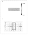
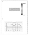
- 4 is a graph of (a) the luminance distribution in a rectangular area positioned at the center of the back surface and (b) the relationship between the luminance and the position on a horizontal line passing through the center of the rectangular area of the lighting device of Example 1
- 8 is a graph of (a) the luminance distribution in a rectangular area positioned at the center of the back surface and (b) the relationship between the position on a horizontal line passing through the center of the rectangular area and the luminance of the lighting device of Example 2
- 8 is a graph of (a) the luminance distribution in a rectangular area located at the center of the back surface and (b) the relationship between the position on a horizontal line passing through the center of the rectangular area and the luminance of the lighting device of Example 3.
- FIG. FIG. 10 is a graph of (a) the luminance distribution in a rectangular area located at the center of the back surface and (b) the relationship between the position on a horizontal line passing through the center of the rectangular area and the luminance of the lighting device of Example 4; 3 is a graph of (a) the luminance distribution in a rectangular area located at the center of the back surface and (b) the relationship between the position on a horizontal line passing through the center of the rectangular area and the luminance of the lighting device of Comparative Example 1; 3 is a graph of (a) the luminance distribution in a rectangular area positioned at the center of the back surface and (b) the relationship between the position on a horizontal line passing through the center of the rectangular area and the luminance of the illumination device of the reference example.
- FIG. 10 is a graph of (a) the luminance distribution in a rectangular area located at the center of the back surface and (b) the relationship between the position on a horizontal line passing through the center of the rectangular area and the luminance of the illumination device of the reference example.
- FIG. 10 is a schematic cross-sectional view of another lighting device 100A1_L according to an embodiment of the present invention
- FIG. 11 is a schematic cross-sectional view of still another lighting device 100A2_L according to an embodiment of the present invention
- FIG. 10 is a schematic cross-sectional view of still another lighting device 100A3_L according to an embodiment of the present invention
- FIG. 11 is a schematic cross-sectional view of a lighting device 900_L for a reference example
- a light guide member for a lighting device and a lighting device according to embodiments of the present invention will be described below with reference to the drawings.
- the light guide member for a lighting device and the lighting device according to the embodiments of the present invention are not limited to those exemplified below.
- FIG. 1 shows a schematic cross-sectional view of a lighting device 100A_L according to an embodiment of the present invention.
- the lighting device 100A_L is a sheet-like lighting device having an emission surface (bottom in FIG. 1) for emitting light LR and a rear surface (upper in FIG. 1) opposite to the emission surface.
- the light LR is emitted in the -Z direction side in FIG.
- the illumination device 100A_L has a light source LS and a light guide member 100A that receives light emitted from the light source LS, propagates the light in the Y direction, and emits the light in the -Z direction.
- the light guide member 100A has a light receiving portion that receives light emitted from the light source LS (for example, the light receiving side surface of the light guide layer 10 on the light source LS side), a first main surface on the light emitting surface side, and a first main surface.
- a light guide layer 10 having a second main surface on the opposite side; a light distribution control structure having a plurality of internal spaces 64; and an antireflection layer 40A disposed therebetween.
- the base layer 32 on which the antireflection layer 40 is formed is arranged on the first main surface side of the light guide layer 10 with the adhesive layer 52 interposed therebetween.
- the exit surface of the lighting device 100A_L is the surface of the antireflection layer 40A opposite to the light guide layer 10 .
- Each of the plurality of internal spaces 64 has a first inclined surface ISa that directs part of the light propagating in the light guide layer 10 toward the output surface side by total internal reflection (TIR), and a side opposite to the first inclined surface ISa. and a second inclined surface ISb.
- the antireflection layer 40A has a single dielectric layer having a refractive index lower than that of the light guide layer 10, or a multi-layer laminate composed of a plurality of dielectric layers having different refractive indices. The antireflection layer 40A prevents the light directed toward the emission surface from being Fresnel-reflected at the interface between the base material layer 32 and the antireflection layer 40A and directed toward the back side.
- the antireflection layer 40A suppresses the Fresnel reflectance to 3% or less.
- Light LR emitted from the emission surface is emitted from the light source LS, propagates through the light guide layer 10, is totally internally reflected by the first inclined surface ISa of the internal space 64, and passes through the light guide layer 10, the base material layer 32, and the light guide layer 32. This is light that has passed through the antireflection layer 40A.
- the light LR may be refracted as it passes through the interface, depending on the refractive index of the material that makes up the interface.
- the light distribution control structure having a plurality of internal spaces 64 is formed in the direction conversion layer 60 arranged on the second main surface side of the light guide layer 10 with the adhesive layer 54 interposed therebetween.
- a redirecting layer 60 having a plurality of internal spaces 64 is composed of a shaping film 62 having recesses 64 (indicated by the same reference numerals as the internal spaces 64 ) on its surface and an adhesive layer 56 .
- a plurality of internal spaces 64 may be formed within the light guide layer 10 .
- a direction changing layer may be formed on the first main surface side of the light guide layer 10 .
- the light distribution control structure is configured such that 80% or more of the light propagating in the light guide layer 10 is directed toward the exit surface side.
- the ratio of the light directed toward the exit surface side can be controlled by adjusting the cross-sectional shape, planar shape, size, arrangement density, and distribution of the internal space 64, for example. can be done.
- the cross-sectional shape of the internal space 64 is triangular as exemplified here, but is not limited to this, and may be trapezoidal or the like.
- the plurality of inner spaces 64 which are the light distribution control structure, correspond to the ratio of the area of the plurality of inner spaces 64 to the area of the light guide layer 10 (occupied area rate) is preferably 1% or more and 80% or less, the upper limit is more preferably 50% or less, further preferably 45% or less, and in order to obtain a high transmittance and / or a low haze value, 30% or less It is preferably 10% or less, more preferably 5% or less. For example, when the occupied area ratio of the internal space is 50%, a haze value of 30% can be obtained.
- the occupied area ratio of the internal space 64 may be uniform, or the occupied area ratio should increase as the distance from the light source LS increases so that the brightness does not decrease. good too.
- the occupied area ratio of the internal space 64 is uniform.
- the base material layer 32 is adhered to the first main surface of the light guide layer 10 with the adhesive layer 52, and the shaping film 62 is adhered to the second main surface of the light guide layer 10 with the adhesive layer 54. is attached. Furthermore, in the light guide member 100 ⁇ /b>A, the base layer 34 and the shaped film 62 are bonded together by the adhesive layer 56 that forms the direction changing layer 60 together with the shaped film 62 .
- the light guide layer 10 and substrate layers 32, 34 may be transparent substrates or films.
- the base material layer 32, the adhesive layer 52, the light guide layer 10, the adhesive layer 54, and the shaped film 62 are designed to have substantially the same refractive index.
- the lighting device 100A_L may have, for example, a visible light transmittance of 60% or more and a haze value of less than 30%.
- the visible light transmittance is preferably 70% or more, more preferably 80% or more.
- the haze value is preferably less than 10%, more preferably 5% or less. Since the light guide member 100A according to the embodiment of the present invention has a high visible light transmittance and a low haze value, objects (displays) can be seen through the light guide member 100A.
- light with a wavelength of 380 nm or more and 780 nm or less is defined as visible light.
- Visible light transmittance and haze value can be measured using, for example, a haze meter (manufactured by Murakami Color Research Laboratory: trade name HM-150).
- FIG. 2 shows a schematic plan view of the lighting device 100A_L.
- the plurality of internal spaces 64 are discretely arranged, for example, in the light guide direction (Y direction) of the light guide layer 10 and in the direction (X direction) orthogonal to the light guide direction.
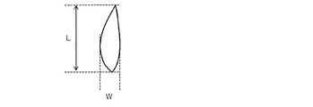
- the size of the internal space 64 (length L, width W: see FIGS. 3A and 3B)
- the length L is preferably 10 ⁇ m or more and 500 ⁇ m or less
- the width W is preferably 1 ⁇ m or more and 100 ⁇ m or less.
- the height H is preferably 1 ⁇ m or more and 100 ⁇ m or less.
- the plurality of internal spaces 64 are discretely arranged in the light guide direction (Y direction) of the light guide layer 10 and in the direction (X direction) orthogonal to the light guide direction.
- the plurality of internal spaces 64 can be discretely arranged in the light guide direction (Y direction) of the light guide layer 10 and in a direction intersecting the light guide direction.
- the discrete arrangement of the internal spaces 64 can be appropriately set according to the shape of the light guide layer 10, the required light distribution, and the like.
- the Y direction is referred to as the light guide direction
- light having a component in the Y direction (not zero) propagates in the Y direction. to The same applies to other directions. That is, light propagating in the -Y direction includes all light having a -Y direction component (not zero).
- the plurality of internal spaces 64 are discretely arranged, for example, in the light guide direction and in a direction intersecting the light guide direction.
- the discrete arrangement may or may not have periodicity (regularity) in at least one direction.
- a plurality of internal spaces 64 having substantially the same shape and convex curved surfaces in the same direction are formed in the light guiding direction (Y direction) of the light guide layer 10 and in the light guiding direction. They are arranged discretely and periodically in the entire area in the orthogonal direction (X direction).
- the pitch Px is preferably, for example, 10 ⁇ m or more and 500 ⁇ m or less
- the pitch Py is, for example, preferably 10 ⁇ m or more and 500 ⁇ m or less.
- the plurality of internal spaces 64 are arranged with a half pitch shift in each of the Y and X directions.
- Px is 200 ⁇ m and Py is 100 ⁇ m.
- the first inclined surface ISa forms a curved surface convex toward the light source LS.
- the light source LS is, for example, an LED device, and a plurality of LED devices are arranged in the X direction along the light receiving portion of the light guide layer 10 . Since the light emitted from each of the plurality of LED devices spreads in the Y direction, it is preferable that the first inclined surface ISa has a curved surface convex toward the light source LS side. acts uniformly on
- the light guide layer 10 has two light receiving portions located on opposite sides, one light receiving portion is provided with the light source LS, and the other light receiving portion is provided with another light source.
- the light distribution control structure may have an internal space 64 including a convex curved surface on the light source LS side, and may not have an internal space including a convex curved surface on the other light source side.
- the light distribution control structure may have an internal space 64 including a convex curved surface on the light source LS side and another internal space including another convex curved surface on the light source side.
- the two types of internal spaces including convex curved surfaces facing opposite sides may be arranged in a mixed manner within the light distribution control structure, or may be arranged separately.
- FIGS. 3A, 3B and 3C show a schematic cross-sectional view of the internal space 64
- FIG. 3B shows a schematic plan view of the internal space 64
- FIG. 3C shows a schematic plan view showing variations of the internal space 64. .
- the cross-sectional shape of the internal space 64 is, for example, triangular. If the inclination angle ⁇ a of the first inclined surface ISa and the inclination angle ⁇ b of the second inclined surface ISb are within the following ranges, 80% or more of the light propagating in the light guide layer 10 can be directed to the exit surface side.
- the inclination angle ⁇ a of the first inclined surface ISa on the light source LS side is, for example, 10° or more and 70° or less. If the inclination angle ⁇ a is less than 10°, the light extraction efficiency may decrease, and if it exceeds 70°, processing may become difficult.
- the inclination angle ⁇ b of the second inclined surface ISb is, for example, 50° or more and 100° or less. If the tilt angle ⁇ b is less than 50°, stray light may occur in undesired directions, and if it exceeds 100°, similarly, the amount of light in undesired directions may increase. Furthermore, in order to increase the amount of light LR emitted from the emission surface and to decrease the amount of light emitted to the viewer side, the inclination angle ⁇ a of the first inclined surface ISa should be, for example, 20° to 50°.
- the inclination angle ⁇ b of the second inclined surface ISb is preferably 70° or more and 90° or less, for example. In Examples 1 to 4 described later, the inclination angle ⁇ a of the first inclined surface ISa is 30°, and the inclination angle ⁇ b of the second inclined surface ISb is 70°.
- the length L of the internal space 64 is preferably 10 ⁇ m or more and 500 ⁇ m or less, and the width W is preferably 1 ⁇ m or more and 100 ⁇ m or less.
- the length L is, for example, twice the width W or more.
- the height H (see FIG. 3A) is preferably 1 ⁇ m or more and 100 ⁇ m or less.
- recesses having the planar shape shown in FIG. 3C may be formed depending on the processing accuracy of the mold. Even in such a case, the planar shape of the internal space can be characterized by the length L and width W. In Examples 1 to 4 described later, the length L of the internal space 64 is 80 ⁇ m, the width W is 20 ⁇ m, and the height H is 10 ⁇ m.
- the antireflection layer 40A not only allows the light LR to be efficiently emitted from the emission surface.
- a problem that occurs when the light guide member 100A does not have the antireflection layer 40A will be described with reference to FIG.
- FIG. 8 shows a schematic cross-sectional view of a lighting device 900_L for a reference example.
- the illumination device 900_L shown in FIG. 8 differs from the illumination device 100A_L shown in FIG. 1 in that the light guide member 900 does not have the adhesive layer 52, the base layer 32 and the antireflection layer 40A.
- most of the light LR1 emitted from the light source LS, propagated through the light guide layer 10, and directed toward the emission surface by the light distribution control structure passes through the first main surface. do.
- 3% to 5% of the light LR2 of the light directed toward the exit surface is Fresnel-reflected by the first main surface.
- the Fresnel-reflected light LR2 enters the internal space 64 from the first inclined surface ISa, passes through the internal space 64, and is emitted in the Z direction from the rear surface of the lighting device 900_L.
- the first inclined surface ISa having a convex curved surface functions as a lens and forms an image of the light LR2 that has passed through the first inclined surface ISa.
- the antireflection layer 40A can suppress the Fresnel reflection of the light directed toward the emission surface side.
- the antireflection layer 40A not only allows the light LR to be efficiently emitted from the exit surface to improve the light extraction efficiency, but also suppresses the generation of a ghost when the lighting device 100A_L is viewed from the rear side, thereby improving the lighting device 100A_L. It has the function of improving designability.
- FIG. 4 shows a schematic cross-sectional view of a lighting device 100B_L according to another embodiment of the invention.
- lighting device 100B_L differs from lighting device 100A_L shown in FIG. 1 in that light guide member 100B has anti-glare layer 40B instead of antireflection layer 40A.
- differences from the lighting device 100A_L shown in FIG. 1 will be mainly described.
- the anti-glare layer 40B is arranged on the first main surface side of the light guide layer 10, and has irregular unevenness on the surface 40BS on the side opposite to the light guide layer 10.
- the exit surface of the lighting device 100B_L is the surface 40BS of the antiglare layer 40B.
- the refractive indices of the anti-glare layer 40B and the substrate layer 32 are designed to be substantially equal to each other, so that light directed toward the exit surface side is Fresnel-reflected at the interface between the anti-glare layer 40B and the substrate layer 32. can be suppressed.
- the anti-glare layer 40B diffuses in various directions the light reflected by the surface 40BS among the light directed toward the emission surface side, thereby suppressing the generation of ghost when the illumination device 100B_L is viewed from the rear side. .
- the illumination device 100B_L becomes cloudy when viewed from the rear side, and the design of the illumination device 100B_L is deteriorated.
- the arithmetic mean roughness Ra of the surface 40BS of the antiglare layer 40B is 0.8 ⁇ m or more and 1000 ⁇ m or less and the maximum height Rz is 5.0 ⁇ m or more and 1000 ⁇ m or less, when the illumination device 100B_L is viewed from the rear side, It is possible to suppress the occurrence of ghosts and suppress cloudiness of the lighting device 100B_L.
- the arithmetic mean roughness Ra and the maximum height Rz can be measured, for example, using a KEYENCE laser microscope VK-X1000 at a magnification of 5 and laser confocal mode.
- the lighting device 100B_L shown in FIG. 4 can have, for example, a visible light transmittance of 60% or more and a haze value of less than 30%, similar to the lighting device 100A_L shown in FIG.
- FIG. 5 shows a schematic cross-sectional view of a lighting device 100C_L according to still another embodiment of the present invention.
- lighting device 100C_L differs from lighting device 100B_L shown in FIG. 4 in that light guide member 100C further includes antireflection layer 40A.
- the exit surface of the lighting device 100C_L is the surface of the antireflection layer 40A opposite to the light guide layer 10 .
- differences from the lighting device 100B_L shown in FIG. 4 will be mainly described.
- the antireflection layer 40A By arranging the antireflection layer 40A on the antiglare layer 40B, it is possible to suppress Fresnel reflection of the light directed toward the emission surface side at the interface between the antiglare layer 40B and the antireflection layer 40A. The reflected light that nevertheless occurs can be diffused in various directions at the surface 40BS. Compared with the lighting device 100B_L shown in FIG. 4, the lighting device 100C_L shown in FIG. The appearance of the lighting device 100C_L can be further improved by further suppressing the occurrence of a ghost when viewing the lighting device 100C_L.
- the lighting device 100C_L shown in FIG. 5 has, for example, a visible light transmittance of 60% or more and a haze value of less than 30%, similar to the lighting device 100A_L shown in FIG. 1 and the lighting device 100B_L shown in FIG. It can have the characteristic that there is
- the refractive index of the constituent elements shown below refers to the refractive index measured with an ellipsometer at a wavelength of 550 nm.
- the lighting device of Example 1 has substantially the same structure as the lighting device 100A_L shown in FIG.
- the light source of Example 1 includes 18 LED devices (Nichia Model No. NS2W266G-HG) arranged at intervals of 6 mm (center-to-center distance between adjacent LEDs) along the light receiving portion.
- the luminous flux of light emitted from each LED was 16.3 lm (20 mA), and the light distribution angle was 120° (the angle at which the brightness intensity is halved).
- the light guide member of Example 1 comprises an antireflection layer/base material layer/acrylic adhesive layer/acrylic plate/acrylic adhesive layer/concavo-convex shaping film/polyester adhesive layer/PET (polyethylene terephthalate) film. It has a laminated structure consisting of The concave-convex shaped film was made of PBT. The light guide member had a width of 120 mm and a length of 170 mm. Table 1 shows the refractive index and thickness of each component other than the base material layer and the antireflection layer contained in the light guide member of Example 1.
- the substrate layer is a TAC (triacetylcellulose) film
- the antireflection layers are, in order from the TAC film, a hard coat layer/a high layer. It has a laminated structure consisting of a refractive index layer/low refractive index layer.
- the hard coat layer was made of acrylic
- the high refractive index layer was made of ZrO
- the low refractive index layer was made of hollow silica.
- Table 2 shows the refractive index and thickness of each component contained in the laminate consisting of the substrate layer and the antireflection layer of Example 1.
- the light guide member of Example 1 can be produced by a known technique.
- the lighting device of Example 2 has substantially the same structure as the lighting device 100A_L shown in FIG.
- the lighting device of Example 2 has the same configuration as that of the lighting device of Example 1, except for the laminate composed of the base material layer and the antireflection layer.
- the base layer is a TAC film
- the antireflection layer is a laminate consisting of a hard coat layer/low refractive layer in order from the side closest to the TAC film. have a structure.
- the hard coat layer was made of acrylic and the low refractive index layer was made of hollow silica.
- Table 3 shows the refractive index and thickness of each component contained in the laminate consisting of the base material layer and the antireflection layer of Example 2.
- the light guide member of Example 2 can be produced by a known method.
- the lighting device of Example 3 has substantially the same structure as the lighting device 100B_L shown in FIG.
- the lighting device of Example 3 has the same configuration as that of the lighting device of Example 1 except for the laminate composed of the base material layer and the antiglare layer.
- the base material layer is a TAC film
- the anti-glare layer is an uneven layer made of PMMA particles.
- the surface of the uneven layer had an arithmetic mean roughness Ra of 1.2 ⁇ m and a maximum height Rz of 6.0 ⁇ m or less.
- Table 4 shows the refractive index and thickness of each component contained in the laminate consisting of the base material layer and the antiglare layer of Example 3.
- the light guide member of Example 3 can be produced by a known method.
- the lighting device of Example 4 has substantially the same structure as the lighting device 100C_L shown in FIG.
- the lighting device of Example 4 has the same configuration as the lighting device of Example 1, except for the laminate composed of the base material layer, the antiglare layer and the antireflection layer.
- the substrate layer is an acrylic film
- the antiglare layer is an uneven layer
- the antireflection layer is a low refractive index layer.
- the uneven layer was made of PMMA particles
- the low refractive index layer was made of hollow silica.
- the surface of the uneven layer had an arithmetic mean roughness Ra of 0.1 ⁇ m and a maximum height Rz of 0.6 ⁇ m or less.
- Table 5 shows the refractive index and thickness of each component contained in the laminate consisting of the substrate layer, antiglare layer and antireflection layer of Example 4.
- the light guide member of Example 4 can be produced by a known method.
- the lighting device of Comparative Example 1 differs from the lighting device of Example 1 in that it has a PET film as a base layer and does not have an antireflection layer.
- the PET film had a refractive index of 1.65 and a thickness of 75 ⁇ m.
- Fresnel reflection of light directed toward the exit surface side is not suppressed.
- the illumination device of the reference example has substantially the same structure as the illumination device 900_L shown in FIG.
- the lighting device of the reference example has a configuration obtained by removing the antireflection layer, the base material layer, and the acrylic adhesive layer disposed on the first main surface side of the acrylic plate from the lighting device of the first embodiment.
- 6A to 6F show, respectively, the luminance in the rectangular area (120 mm in the width direction and 48.5 mm in the length direction) located in the center of the back surface of the lighting devices of Examples 1 to 4, Comparative Example and Reference Example. 3 shows a graph of the distribution and (b) the relationship between the position on a horizontal line (parallel to the width direction) passing through the center of the rectangular area and the luminance.
- Table 6 shows the maximum luminance contrast ratio and presence or absence of ghost generation at specific portions on the back surface of the illumination devices of Examples 1 to 4, Comparative Example 1, and Reference Example.
- the luminance at a specific portion on the back surface is the luminance at a 17.3 mm long portion symmetrical with respect to the center of the horizontal line passing through the center of the above rectangular area ((b ), see the area enclosed by the bold line).
- the maximum contrast ratio of luminance at a specific portion on the back surface was 1.1 or less.
- the inventor investigated the maximum brightness contrast ratio in a square area (17.3 mm) located at an arbitrary location in the area where light leaks from the back of the lighting device.
- the term “light-leaking region” means a region of the rear surface whose luminance is 70% or more of the maximum luminance.
- the maximum luminance contrast ratio in the above-described square areas located at arbitrary locations was 1.1 or less.
- the haze values of the lighting devices of Examples 1 to 4 were 4.0% or less, and the lighting devices hardly became cloudy. Furthermore, the lighting devices of Examples 1 to 4 had a luminous reflectance Y of 2.0% or less, and the lighting devices had high transparency.
- FIGS. 7A, 7B, and 7C show examples of lighting devices having the same light distribution control structure as lighting device 100A_L shown in FIG.
- the lighting device 100A1_L shown in FIG. 7A differs from the lighting device 100A_L shown in FIG. 1 in that the hard coat layer 70 is arranged on the base material layer 34 via the adhesive layer 58 .
- the hard coat layer 70 may have a pencil hardness of H or higher, for example.
- the hard coat layer 70 can improve the scratch resistance of the surface of the lighting device 100A1_L.
- the illumination device 100A2_L shown in FIG. 7B differs from the illumination device 100A_L shown in FIG. 1 in that the low refractive index layer 20 is arranged instead of the base material layer 34 .
- the light emitted from the light source LS passes through the shaping film 62 without passing through the internal space 64, and travels toward the base material layer 34 at the interface between the base material layer 34 and the air. It is totally internally reflected and directed toward the exit surface. If the top surface of the base material layer 34 is dirty, total internal reflection may not occur in the dirty portion. As a result, problems such as leakage of light from the soiled portion and/or a change in the distribution of light propagating in the light guide member occur.
- the interface between the shaping film 62 and the low refractive index layer 20 becomes an interface capable of internal total reflection of the light propagating through the shaping film 62 .
- the “interface between the shaping film 62 and the low refractive index layer 20” refers to the interface between the shaping film 62 and the adhesive layer 56, the interface between the low refractive index layer 20 and the adhesive layer 56, and/or both interfaces. means the area between Light propagating through the shaping film 62 is not affected by the state of the interface between the low refractive index layer 20 and air. Therefore, the low refractive index layer 20 can improve the antifouling property of the surface of the lighting device 100A2_L.
- the lighting device 100A3_L shown in FIG. 7C differs from the lighting device 100A2_L shown in FIG. 7B in that the hard coat layer 70 is arranged on the low refractive index layer 20 with the adhesive layer 58 interposed therebetween.
- the hard coat layer 70 and the low refractive index layer 20 can improve the scratch resistance and antifouling properties of the surface of the lighting device 100A2_L, respectively.
- the hard coat layer 70 and the low refractive index layer 20 can be formed by a known method using known materials. These can also be applied to lighting devices 100B_L according to other embodiments of the invention and lighting devices 100C_L according to still other embodiments of the invention.
- a shaping film for forming an internal space can be manufactured, for example, as follows.
- a concave-convex shaped film was produced according to the method described in JP-T-2013-524288. Specifically, the surface of a polymethyl methacrylate (PMMA) film is coated with lacquer (Fine Cure RM-64 manufactured by Sanyo Chemical Industries, Ltd.), an optical pattern is embossed on the film surface containing the lacquer, and then the lacquer is applied. was cured to produce the desired concave-convex shaped film.
- the unevenness-imparting film had a total thickness of 130 ⁇ m and a haze of 0.8%.
- the light guide layer 10 is made of a known material with high visible light transmittance.
- the light guide layer 10 is made of, for example, an acrylic resin such as polymethyl methacrylate (PMMA), a polycarbonate (PC) resin, a cycloolefin resin, or glass (for example, quartz glass, alkali-free glass, or borosilicate glass). be.
- the refractive index n GP of the light guide layer 10 is, for example, 1.40 or more and 1.80 or less.
- the thickness of the light guide layer 10 can be appropriately set according to the application.
- the thickness of the light guide layer 10 is, for example, 0.05 mm or more and 50 mm or less.
- the thickness of the base material layers 32 and 34 is, for example, 1 ⁇ m or more and 1000 ⁇ m or less, preferably 10 ⁇ m or more and 100 ⁇ m or less, and more preferably 20 ⁇ m or more and 80 ⁇ m.
- the refractive indices of the substrate layers 32 and 34 are each independently preferably 1.40 or more and 1.70 or less, more preferably 1.43 or more and 1.65 or less.
- the thicknesses of the adhesive layers 52, 54, 56, and 58 are each independently, for example, 0.1 ⁇ m or more and 100 ⁇ m or less, preferably 0.3 ⁇ m or more and 100 ⁇ m or less, and more preferably 0.5 ⁇ m or more and 50 ⁇ m or less.
- the refractive indices of the adhesive layers 52, 54, 56 and 58 are each independently preferably 1.42 or more and 1.60 or less, more preferably 1.47 or more and 1.58 or less.
- the refractive index of the adhesive layers 52, 54, 56, and 58 is preferably close to the refractive index of the light guide layer 10 or the shaping film 62 with which it is in contact, and the absolute value of the refractive index difference is 0.2 or less. is preferably
- the adhesive layer 56 can adhere without filling the concave portions 64 on the surface of the shaping film 62 .
- the adhesive described in International Publication No. 2021/167090, International Publication No. 2021/167091, or International Application PCT/JP2022/004554 by the present applicant is preferably used. be able to. The entire disclosure of these applications is incorporated herein by reference.
- the polyester-based adhesive described in International Application PCT/JP2022/004554 is preferred.
- the antireflection layer 40A may be a single low refractive index layer, but is preferably an alternate laminate of high refractive index layers and low refractive index layers.
- the high refractive index layer has, for example, a refractive index of 1.9 or more, preferably 2.0 or more.
- high refractive index materials include titanium oxide, niobium oxide, zirconium oxide, tantalum oxide, zinc oxide, indium oxide, indium tin oxide (ITO), and antimony-doped tin oxide (ATO). Among them, titanium oxide or niobium oxide is preferable.
- the low refractive index layer has, for example, a refractive index of 1.6 or less, preferably 1.5 or less.
- low refractive index materials include silicon oxide, titanium nitride, magnesium fluoride, barium fluoride, calcium fluoride, hafnium fluoride, and lanthanum fluoride.
- silicon oxide is preferred.
- a medium refractive index layer having a refractive index of about 1.6 to 1.9 may be provided in addition to the low refractive index layer and the high refractive index layer.
- the film thicknesses of the high refractive index layer and the low refractive index layer are each about 5 nm or more and 200 nm or less, preferably about 15 nm or more and 150 nm or less.
- the film thickness of each layer may be designed so that the reflectance of visible light is reduced according to the refractive index, lamination structure, and the like.
- the antireflection layer 40A is preferably laminated on the hard coat layer via a primer layer.
- materials constituting the primer layer include metals such as silicon, nickel, chromium, tin, gold, silver, platinum, zinc, titanium, tungsten, aluminum, zirconium, and palladium; alloys of these metals; oxides, fluorides, sulfides or nitrides; Among them, the material of the primer layer is preferably an oxide, and particularly preferably silicon oxide.
- the primer layer is preferably an inorganic oxide layer with less than stoichiometric oxygen content. Among inorganic oxides having a non-stoichiometric composition, silicon oxide represented by the composition formula SiO x (0.5 ⁇ x ⁇ 2) is preferable.
- the thickness of the primer layer is, for example, about 1 nm or more and 20 nm or less, preferably 3 nm or more and 15 nm or less.
- the method of forming the thin film forming the antireflection layer 40A is not particularly limited, and either a wet coating method or a dry coating method may be used.
- a dry coating method such as vacuum deposition, CVD, sputtering, or electron beam deposition is preferable because a thin film having a uniform thickness can be formed.
- the sputtering method is preferable because it is excellent in uniformity of film thickness and easy to form a dense film.
- the antireflection layer described in JP-A-2020-52221 can be preferably used.
- the entire disclosure of Japanese Patent Application Laid-Open No. 2020-52221 is incorporated herein by reference.
- the antireflection layer 40A does not have to have the above-described single low refractive index layer or the alternate laminate of high refractive index layers and low refractive index layers.
- the antireflection layer 40A may have a so-called moth-eye structure.
- the antireflection layer 40A may be made of a material having voids, like the low refractive index layer 20 described below.
- the refractive indices n L1 of the low refractive index layers 20 are each independently, for example, preferably 1.30 or less, more preferably 1.20 or less, and even more preferably 1.15 or less.
- the low refractive index layer 20 is preferably solid, and preferably has a refractive index of, for example, 1.05 or more.
- the difference between the refractive index of the light guide layer 10 and the refractive index layer of the low refractive index layer 20 is preferably 0.20 or more, more preferably 0.23 or more, and still more preferably 0.25 or more.
- the low refractive index layer 20 having a refractive index of 1.30 or less can be formed using, for example, a porous material.
- Each of the low refractive index layers 20 has a thickness independently of, for example, 0.3 ⁇ m or more and 5 ⁇ m or less.
- the porosity is preferably 35% by volume or more, more preferably 38% by volume or more, and particularly preferably 40% by volume or more. . Within such a range, a low refractive index layer having a particularly low refractive index can be formed.
- the upper limit of the porosity of the low refractive index layer is, for example, 90% by volume or less, preferably 75% by volume or less. Within such a range, a low refractive index layer having excellent strength can be formed.
- the porosity is a value calculated by Lorentz-Lorenz's formula from refractive index values measured by an ellipsometer.
- the low refractive index layer for example, a low refractive index layer having voids disclosed in Patent Document 3 can be used.
- the low refractive index layer having voids is a porous body formed by directly chemically bonding particles (for example, microporous particles) to each other.
- the particles constituting the low refractive index layer having voids may be bonded together via a small amount (for example, the mass of the particles or less) of one component of the binder.
- the porosity and refractive index of the low refractive index layer can be adjusted by the particle size, particle size distribution, etc. of the particles forming the low refractive index layer.
- Methods for obtaining a low refractive index layer having voids include, for example, JP-A-2010-189212, JP-A-2008-040171, JP-A-2006-011175, International Publication No. 2004/113966, and their Methods described in ref. All of the disclosures of JP-A-2010-189212, JP-A-2008-040171, JP-A-2006-011175, and International Publication No. 2004/113966 are incorporated herein by reference.
- a silica porous material can be preferably used as the low refractive index layer having voids.
- a silica porous body is produced, for example, by the following method. a silicon compound; hydrolyzable silanes and/or silsesquioxane, and a method of hydrolyzing and polycondensing at least one of its partial hydrolyzate and dehydration condensate; porous particles and/or hollow fine particles; method, method of generating an airgel layer using the springback phenomenon, pulverizing the gel-like silicon compound obtained by the sol-gel method, and chemically pulverizing the resulting pulverized microporous particles with a catalyst or the like. and a method using a combined pulverized gel.
- the low refractive index layer is not limited to the porous silica material, nor is the manufacturing method limited to the exemplified manufacturing method, and may be manufactured by any manufacturing method.
- the porous layer is not limited to the silica porous body, and the manufacturing method is not limited to the exemplified manufacturing method, and may be manufactured by any manufacturing method.
- Silsesquioxane is a silicon compound having (RSiO 1.5 , R is a hydrocarbon group) as a basic structural unit, and is strictly different from silica having SiO 2 as a basic structural unit.
- a porous material containing silsesquioxane as a basic structural unit is also referred to herein as a silica porous material or a silica-based porous material, since it has a network structure crosslinked with silica in common.
- the silica porous body can be composed of microporous particles of a gel-like silicon compound bonded together.
- pulverized bodies of the gelled silicon compound can be mentioned.
- the silica porous body can be formed, for example, by coating a base material with a coating liquid containing a pulverized gel-like silicon compound.
- the pulverized gel-like silicon compound can be chemically bonded (for example, siloxane bond) by the action of a catalyst, light irradiation, heating, or the like.
- the hardness HH1 of the hard coat layer 70 is, for example, preferably a pencil hardness of H or higher, more preferably 2H or higher, and more preferably 4H or higher.
- the upper limit of the hardness HH1 of the hard coat layer 70 is not particularly limited, but is preferably 6H or less in pencil hardness, more preferably 5H or less.
- Pencil hardness is measured by a method conforming to JIS K 5400 "Pencil Hardness Test".
- the thickness of each hard coat layer 70 is preferably 1 ⁇ m or more and 30 ⁇ m or less, more preferably 2 ⁇ m or more and 20 ⁇ m or less, and still more preferably 3 ⁇ m or more and 15 ⁇ m or less. If the thickness of the hard coat layer 70 is within such a range, it has good scratch resistance.
- the hard coat layer 70 can be made of any appropriate material as long as it satisfies the above properties.
- the hard coat layer 70 is, for example, a cured layer of thermosetting resin or ionizing radiation (eg, visible light, ultraviolet) curable resin.
- curable resins include acrylates such as urethane (meth)acrylate, polyester (meth)acrylate and epoxy (meth)acrylate, silicon resins such as polysiloxane, unsaturated polyesters, and epoxy resins.
- the hard coat layer 70 can be formed, for example, by applying a material containing a solvent and a curable compound to the surface of the target substrate and curing the material. Details of the hard coat layer suitably used as the hard coat layer 70 are described in, for example, JP-A-2011-237789. The entire disclosure of JP-A-2011-237789 is incorporated herein by reference.
- a light guide member for an illuminating device and an illuminating device according to an embodiment of the present invention can emit light from one of two main surfaces facing in opposite directions, and emit light from the other main surface. Appears transparent when viewed.
- INDUSTRIAL APPLICABILITY The light guide member for a lighting device and the lighting device according to the embodiment of the present invention can provide new uses that combine practicality and design.
- 10 light guide layer
- 20 low refractive index layer
- 32, 34 base layer
- 40A antireflection layer
- 40B antiglare layer
- 52, 54, 56, 58 adhesive layer
- 60 direction changing layer
- 62 Shaping film
- 64 Internal space, concave portion
- 70 Hard coat layer
- 900 Light guide member for lighting device
- 900_L Lighting device
- ISa First slope surface
- ISb second inclined surface
- LR, LR1, LR2 light
- LS light source
Landscapes
- Physics & Mathematics (AREA)
- General Physics & Mathematics (AREA)
- Optics & Photonics (AREA)
- Engineering & Computer Science (AREA)
- General Engineering & Computer Science (AREA)
- Planar Illumination Modules (AREA)
- Non-Portable Lighting Devices Or Systems Thereof (AREA)
Priority Applications (5)
| Application Number | Priority Date | Filing Date | Title |
|---|---|---|---|
| CN202280043047.9A CN117501043A (zh) | 2021-06-17 | 2022-06-10 | 照明装置用导光部件以及照明装置 |
| EP22824920.7A EP4357663A4 (en) | 2021-06-17 | 2022-06-10 | Light guide member for lighting device and lighting device |
| JP2023529838A JPWO2022264930A1 (https=) | 2021-06-17 | 2022-06-10 | |
| KR1020237043443A KR20240022496A (ko) | 2021-06-17 | 2022-06-10 | 조명 장치용 도광 부재 및 조명 장치 |
| US18/570,874 US12210181B2 (en) | 2021-06-17 | 2022-06-10 | Light guide member for lighting device and lighting device |
Applications Claiming Priority (2)
| Application Number | Priority Date | Filing Date | Title |
|---|---|---|---|
| JP2021100994 | 2021-06-17 | ||
| JP2021-100994 | 2021-06-17 |
Publications (1)
| Publication Number | Publication Date |
|---|---|
| WO2022264930A1 true WO2022264930A1 (ja) | 2022-12-22 |
Family
ID=84527479
Family Applications (1)
| Application Number | Title | Priority Date | Filing Date |
|---|---|---|---|
| PCT/JP2022/023417 Ceased WO2022264930A1 (ja) | 2021-06-17 | 2022-06-10 | 照明装置用導光部材および照明装置 |
Country Status (7)
| Country | Link |
|---|---|
| US (1) | US12210181B2 (https=) |
| EP (1) | EP4357663A4 (https=) |
| JP (1) | JPWO2022264930A1 (https=) |
| KR (1) | KR20240022496A (https=) |
| CN (1) | CN117501043A (https=) |
| TW (1) | TW202314352A (https=) |
| WO (1) | WO2022264930A1 (https=) |
Families Citing this family (2)
| Publication number | Priority date | Publication date | Assignee | Title |
|---|---|---|---|---|
| WO2022260080A1 (ja) * | 2021-06-09 | 2022-12-15 | 日東電工株式会社 | 照明装置用導光部材および照明装置 |
| TWI889136B (zh) * | 2024-01-10 | 2025-07-01 | 李裕翔 | 導光件 |
Citations (17)
| Publication number | Priority date | Publication date | Assignee | Title |
|---|---|---|---|---|
| JP2000048617A (ja) * | 1998-07-28 | 2000-02-18 | Nitto Denko Corp | 導光板、面光源装置及び反射型液晶表示装置 |
| JP2004113966A (ja) | 2002-09-27 | 2004-04-15 | Kurashiki Seni Kako Kk | 生分解性空気清浄用フィルター |
| JP2006011175A (ja) | 2004-06-28 | 2006-01-12 | Pentax Corp | 反射防止膜を有する光学素子及びその製造方法 |
| JP2007200768A (ja) * | 2006-01-27 | 2007-08-09 | Nippon Leiz Co Ltd | 導光板および平面照明装置 |
| JP2008040171A (ja) | 2006-08-07 | 2008-02-21 | Pentax Corp | セルフクリーニング効果を有する反射防止膜を設けた光学素子及びその製造方法 |
| JP2010189212A (ja) | 2009-02-17 | 2010-09-02 | Shinshu Univ | 多孔質シリカ膜およびその製造方法 |
| JP2011133879A (ja) * | 2009-11-30 | 2011-07-07 | Nitto Denko Corp | 液晶表示装置 |
| WO2011124765A1 (en) | 2010-04-06 | 2011-10-13 | Kari Rinko | Laminate structure with embedded cavities and related method of manufacture |
| JP2011237789A (ja) | 2010-04-15 | 2011-11-24 | Nitto Denko Corp | ハードコートフィルム、偏光板、画像表示装置、及びハードコートフィルムの製造方法 |
| JP2013197065A (ja) * | 2012-03-22 | 2013-09-30 | Skg:Kk | 照明装置 |
| WO2019087118A1 (en) | 2017-11-01 | 2019-05-09 | Nitto Denko Corporation | Light distribution structure and element, related method and uses |
| WO2019102959A1 (ja) | 2017-11-21 | 2019-05-31 | 富士フイルム株式会社 | 片面照明兼用窓 |
| WO2019146628A1 (ja) | 2018-01-26 | 2019-08-01 | 日東電工株式会社 | Led照明器具用フィルム、led照明器具 |
| WO2019182091A1 (ja) | 2018-03-22 | 2019-09-26 | 日東電工株式会社 | 光学デバイス |
| JP2020052221A (ja) | 2018-09-26 | 2020-04-02 | 日東電工株式会社 | 保護フィルム付き光学フィルム |
| WO2021167091A1 (ja) | 2020-02-21 | 2021-08-26 | 日東電工株式会社 | 接着剤組成物層、積層体、光学積層体および光学装置、ならびに光学積層体の製造方法 |
| WO2021167090A1 (ja) | 2020-02-21 | 2021-08-26 | 日東電工株式会社 | 接着剤層、積層体、光学積層体および光学積層体の製造方法、ならびに光学装置 |
Family Cites Families (6)
| Publication number | Priority date | Publication date | Assignee | Title |
|---|---|---|---|---|
| DE69930025T2 (de) | 1998-04-17 | 2006-08-10 | Nitto Denko Corp., Ibaraki | Lichtleitende Platte, Oberfläche- Lichtquellenvorrichtung, und Reflexion-Type Flüssigkristall Anzeige |
| JP2002189106A (ja) * | 2000-12-20 | 2002-07-05 | Dainippon Printing Co Ltd | 防眩性フィルムおよびその製造方法、ならびに防眩性フィルムを用いた表示装置 |
| JP4122161B2 (ja) * | 2002-02-04 | 2008-07-23 | 日本電産コパル株式会社 | 面発光装置 |
| JP5512380B2 (ja) * | 2010-04-30 | 2014-06-04 | 株式会社フジクラ | 表示装置 |
| US20210148545A1 (en) * | 2019-11-20 | 2021-05-20 | Glint Photonics, Inc. | Antireflective optics for lighting products |
| WO2022260080A1 (ja) * | 2021-06-09 | 2022-12-15 | 日東電工株式会社 | 照明装置用導光部材および照明装置 |
-
2022
- 2022-06-10 JP JP2023529838A patent/JPWO2022264930A1/ja active Pending
- 2022-06-10 US US18/570,874 patent/US12210181B2/en active Active
- 2022-06-10 WO PCT/JP2022/023417 patent/WO2022264930A1/ja not_active Ceased
- 2022-06-10 EP EP22824920.7A patent/EP4357663A4/en active Pending
- 2022-06-10 KR KR1020237043443A patent/KR20240022496A/ko active Pending
- 2022-06-10 CN CN202280043047.9A patent/CN117501043A/zh active Pending
- 2022-06-16 TW TW111122375A patent/TW202314352A/zh unknown
Patent Citations (17)
| Publication number | Priority date | Publication date | Assignee | Title |
|---|---|---|---|---|
| JP2000048617A (ja) * | 1998-07-28 | 2000-02-18 | Nitto Denko Corp | 導光板、面光源装置及び反射型液晶表示装置 |
| JP2004113966A (ja) | 2002-09-27 | 2004-04-15 | Kurashiki Seni Kako Kk | 生分解性空気清浄用フィルター |
| JP2006011175A (ja) | 2004-06-28 | 2006-01-12 | Pentax Corp | 反射防止膜を有する光学素子及びその製造方法 |
| JP2007200768A (ja) * | 2006-01-27 | 2007-08-09 | Nippon Leiz Co Ltd | 導光板および平面照明装置 |
| JP2008040171A (ja) | 2006-08-07 | 2008-02-21 | Pentax Corp | セルフクリーニング効果を有する反射防止膜を設けた光学素子及びその製造方法 |
| JP2010189212A (ja) | 2009-02-17 | 2010-09-02 | Shinshu Univ | 多孔質シリカ膜およびその製造方法 |
| JP2011133879A (ja) * | 2009-11-30 | 2011-07-07 | Nitto Denko Corp | 液晶表示装置 |
| WO2011124765A1 (en) | 2010-04-06 | 2011-10-13 | Kari Rinko | Laminate structure with embedded cavities and related method of manufacture |
| JP2011237789A (ja) | 2010-04-15 | 2011-11-24 | Nitto Denko Corp | ハードコートフィルム、偏光板、画像表示装置、及びハードコートフィルムの製造方法 |
| JP2013197065A (ja) * | 2012-03-22 | 2013-09-30 | Skg:Kk | 照明装置 |
| WO2019087118A1 (en) | 2017-11-01 | 2019-05-09 | Nitto Denko Corporation | Light distribution structure and element, related method and uses |
| WO2019102959A1 (ja) | 2017-11-21 | 2019-05-31 | 富士フイルム株式会社 | 片面照明兼用窓 |
| WO2019146628A1 (ja) | 2018-01-26 | 2019-08-01 | 日東電工株式会社 | Led照明器具用フィルム、led照明器具 |
| WO2019182091A1 (ja) | 2018-03-22 | 2019-09-26 | 日東電工株式会社 | 光学デバイス |
| JP2020052221A (ja) | 2018-09-26 | 2020-04-02 | 日東電工株式会社 | 保護フィルム付き光学フィルム |
| WO2021167091A1 (ja) | 2020-02-21 | 2021-08-26 | 日東電工株式会社 | 接着剤組成物層、積層体、光学積層体および光学装置、ならびに光学積層体の製造方法 |
| WO2021167090A1 (ja) | 2020-02-21 | 2021-08-26 | 日東電工株式会社 | 接着剤層、積層体、光学積層体および光学積層体の製造方法、ならびに光学装置 |
Non-Patent Citations (1)
| Title |
|---|
| See also references of EP4357663A4 |
Also Published As
| Publication number | Publication date |
|---|---|
| CN117501043A (zh) | 2024-02-02 |
| JPWO2022264930A1 (https=) | 2022-12-22 |
| TW202314352A (zh) | 2023-04-01 |
| US12210181B2 (en) | 2025-01-28 |
| US20240219620A1 (en) | 2024-07-04 |
| EP4357663A1 (en) | 2024-04-24 |
| KR20240022496A (ko) | 2024-02-20 |
| EP4357663A4 (en) | 2025-05-21 |
Similar Documents
| Publication | Publication Date | Title |
|---|---|---|
| CN101836136B (zh) | 防眩膜、防眩性偏振板及图像显示装置 | |
| TWI497105B (zh) | 多功能複合型光學膜 | |
| KR102814283B1 (ko) | 조명 장치용 도광부재, 조명 장치 및 건축부재 | |
| WO2022264930A1 (ja) | 照明装置用導光部材および照明装置 | |
| TW201015159A (en) | Structure for multi-layer coating composite optical film | |
| KR101676901B1 (ko) | 광학 성능이 우수한 광학 필름 적층체 및 이를 포함하는 백라이트 유닛 | |
| TW201505847A (zh) | 積層體、積層體的製造方法、光源裝置用導光體及光源裝置 | |
| TW202314303A (zh) | 發光裝置用導光構件及發光裝置 | |
| JP2017219619A (ja) | 映像源ユニット | |
| JP2009258666A (ja) | 機能性部材、光学部品、バックライトユニット及び表示装置 | |
| JP7462840B2 (ja) | 照明装置用導光部材および照明装置 | |
| WO2023276836A1 (ja) | 照明装置用導光部材および照明装置 | |
| WO2015020031A1 (ja) | 積層体の製造方法、積層体、光源装置用導光体及び光源装置 | |
| JP4410840B2 (ja) | 光学調整部材、並びに、それを備える照明装置及び液晶表示装置 | |
| WO2023276705A1 (ja) | 光学積層体および照明装置 | |
| JP2014082095A (ja) | 導光体および面光源装置 | |
| WO2024070908A1 (ja) | 照明装置 | |
| TW202542566A (zh) | 導光體及照明裝置 | |
| TW202613450A (zh) | 賦形膜、積層體、附有導光層之積層體、照明裝置及模具 | |
| WO2022244474A1 (ja) | 光学装置 | |
| TW202613612A (zh) | 導光體及照明裝置 | |
| WO2024070909A1 (ja) | 光学装置、光学部材および導光部材 | |
| KR20150092654A (ko) | 조명 부재 및 이를 이용하는 조명 장치 | |
| JP4410841B2 (ja) | 照明装置及び液晶表示装置 | |
| JP6066564B2 (ja) | 照明装置 |
Legal Events
| Date | Code | Title | Description |
|---|---|---|---|
| 121 | Ep: the epo has been informed by wipo that ep was designated in this application |
Ref document number: 22824920 Country of ref document: EP Kind code of ref document: A1 |
|
| WWE | Wipo information: entry into national phase |
Ref document number: 202280043047.9 Country of ref document: CN Ref document number: 18570874 Country of ref document: US Ref document number: 2023529838 Country of ref document: JP |
|
| WWE | Wipo information: entry into national phase |
Ref document number: 2022824920 Country of ref document: EP |
|
| NENP | Non-entry into the national phase |
Ref country code: DE |
|
| ENP | Entry into the national phase |
Ref document number: 2022824920 Country of ref document: EP Effective date: 20240117 |