WO2022259593A1 - 電界効果トランジスタとその製造方法 - Google Patents
電界効果トランジスタとその製造方法 Download PDFInfo
- Publication number
- WO2022259593A1 WO2022259593A1 PCT/JP2022/001571 JP2022001571W WO2022259593A1 WO 2022259593 A1 WO2022259593 A1 WO 2022259593A1 JP 2022001571 W JP2022001571 W JP 2022001571W WO 2022259593 A1 WO2022259593 A1 WO 2022259593A1
- Authority
- WO
- WIPO (PCT)
- Prior art keywords
- region
- trench
- gate insulating
- breakdown voltage
- insulating film
- Prior art date
- Legal status (The legal status is an assumption and is not a legal conclusion. Google has not performed a legal analysis and makes no representation as to the accuracy of the status listed.)
- Ceased
Links
Images









Classifications
-
- H—ELECTRICITY
- H10—SEMICONDUCTOR DEVICES; ELECTRIC SOLID-STATE DEVICES NOT OTHERWISE PROVIDED FOR
- H10D—INORGANIC ELECTRIC SEMICONDUCTOR DEVICES
- H10D30/00—Field-effect transistors [FET]
- H10D30/01—Manufacture or treatment
- H10D30/021—Manufacture or treatment of FETs having insulated gates [IGFET]
-
- H—ELECTRICITY
- H10—SEMICONDUCTOR DEVICES; ELECTRIC SOLID-STATE DEVICES NOT OTHERWISE PROVIDED FOR
- H10D—INORGANIC ELECTRIC SEMICONDUCTOR DEVICES
- H10D30/00—Field-effect transistors [FET]
- H10D30/01—Manufacture or treatment
- H10D30/021—Manufacture or treatment of FETs having insulated gates [IGFET]
- H10D30/028—Manufacture or treatment of FETs having insulated gates [IGFET] of double-diffused metal oxide semiconductor [DMOS] FETs
- H10D30/0291—Manufacture or treatment of FETs having insulated gates [IGFET] of double-diffused metal oxide semiconductor [DMOS] FETs of vertical DMOS [VDMOS] FETs
- H10D30/0297—Manufacture or treatment of FETs having insulated gates [IGFET] of double-diffused metal oxide semiconductor [DMOS] FETs of vertical DMOS [VDMOS] FETs using recessing of the gate electrodes, e.g. to form trench gate electrodes
-
- H—ELECTRICITY
- H10—SEMICONDUCTOR DEVICES; ELECTRIC SOLID-STATE DEVICES NOT OTHERWISE PROVIDED FOR
- H10D—INORGANIC ELECTRIC SEMICONDUCTOR DEVICES
- H10D30/00—Field-effect transistors [FET]
- H10D30/60—Insulated-gate field-effect transistors [IGFET]
-
- H—ELECTRICITY
- H10—SEMICONDUCTOR DEVICES; ELECTRIC SOLID-STATE DEVICES NOT OTHERWISE PROVIDED FOR
- H10D—INORGANIC ELECTRIC SEMICONDUCTOR DEVICES
- H10D30/00—Field-effect transistors [FET]
- H10D30/60—Insulated-gate field-effect transistors [IGFET]
- H10D30/64—Double-diffused metal-oxide semiconductor [DMOS] FETs
- H10D30/66—Vertical DMOS [VDMOS] FETs
- H10D30/668—Vertical DMOS [VDMOS] FETs having trench gate electrodes, e.g. UMOS transistors
-
- H—ELECTRICITY
- H10—SEMICONDUCTOR DEVICES; ELECTRIC SOLID-STATE DEVICES NOT OTHERWISE PROVIDED FOR
- H10D—INORGANIC ELECTRIC SEMICONDUCTOR DEVICES
- H10D62/00—Semiconductor bodies, or regions thereof, of devices having potential barriers
- H10D62/01—Manufacture or treatment
- H10D62/051—Forming charge compensation regions, e.g. superjunctions
-
- H—ELECTRICITY
- H10—SEMICONDUCTOR DEVICES; ELECTRIC SOLID-STATE DEVICES NOT OTHERWISE PROVIDED FOR
- H10D—INORGANIC ELECTRIC SEMICONDUCTOR DEVICES
- H10D62/00—Semiconductor bodies, or regions thereof, of devices having potential barriers
- H10D62/10—Shapes, relative sizes or dispositions of the regions of the semiconductor bodies; Shapes of the semiconductor bodies
- H10D62/102—Constructional design considerations for preventing surface leakage or controlling electric field concentration
- H10D62/103—Constructional design considerations for preventing surface leakage or controlling electric field concentration for increasing or controlling the breakdown voltage of reverse-biased devices
- H10D62/105—Constructional design considerations for preventing surface leakage or controlling electric field concentration for increasing or controlling the breakdown voltage of reverse-biased devices by having particular doping profiles, shapes or arrangements of PN junctions; by having supplementary regions, e.g. junction termination extension [JTE]
- H10D62/106—Constructional design considerations for preventing surface leakage or controlling electric field concentration for increasing or controlling the breakdown voltage of reverse-biased devices by having particular doping profiles, shapes or arrangements of PN junctions; by having supplementary regions, e.g. junction termination extension [JTE] having supplementary regions doped oppositely to or in rectifying contact with regions of the semiconductor bodies, e.g. guard rings with PN or Schottky junctions
- H10D62/107—Buried supplementary regions, e.g. buried guard rings
-
- H—ELECTRICITY
- H10—SEMICONDUCTOR DEVICES; ELECTRIC SOLID-STATE DEVICES NOT OTHERWISE PROVIDED FOR
- H10D—INORGANIC ELECTRIC SEMICONDUCTOR DEVICES
- H10D62/00—Semiconductor bodies, or regions thereof, of devices having potential barriers
- H10D62/10—Shapes, relative sizes or dispositions of the regions of the semiconductor bodies; Shapes of the semiconductor bodies
- H10D62/102—Constructional design considerations for preventing surface leakage or controlling electric field concentration
- H10D62/103—Constructional design considerations for preventing surface leakage or controlling electric field concentration for increasing or controlling the breakdown voltage of reverse-biased devices
- H10D62/105—Constructional design considerations for preventing surface leakage or controlling electric field concentration for increasing or controlling the breakdown voltage of reverse-biased devices by having particular doping profiles, shapes or arrangements of PN junctions; by having supplementary regions, e.g. junction termination extension [JTE]
- H10D62/109—Reduced surface field [RESURF] PN junction structures
- H10D62/111—Multiple RESURF structures, e.g. double RESURF or 3D-RESURF structures
-
- H—ELECTRICITY
- H10—SEMICONDUCTOR DEVICES; ELECTRIC SOLID-STATE DEVICES NOT OTHERWISE PROVIDED FOR
- H10D—INORGANIC ELECTRIC SEMICONDUCTOR DEVICES
- H10D62/00—Semiconductor bodies, or regions thereof, of devices having potential barriers
- H10D62/10—Shapes, relative sizes or dispositions of the regions of the semiconductor bodies; Shapes of the semiconductor bodies
- H10D62/124—Shapes, relative sizes or dispositions of the regions of semiconductor bodies or of junctions between the regions
- H10D62/126—Top-view geometrical layouts of the regions or the junctions
- H10D62/127—Top-view geometrical layouts of the regions or the junctions of cellular field-effect devices, e.g. multicellular DMOS transistors or IGBTs
-
- H—ELECTRICITY
- H10—SEMICONDUCTOR DEVICES; ELECTRIC SOLID-STATE DEVICES NOT OTHERWISE PROVIDED FOR
- H10D—INORGANIC ELECTRIC SEMICONDUCTOR DEVICES
- H10D62/00—Semiconductor bodies, or regions thereof, of devices having potential barriers
- H10D62/10—Shapes, relative sizes or dispositions of the regions of the semiconductor bodies; Shapes of the semiconductor bodies
- H10D62/13—Semiconductor regions connected to electrodes carrying current to be rectified, amplified or switched, e.g. source or drain regions
- H10D62/149—Source or drain regions of field-effect devices
- H10D62/151—Source or drain regions of field-effect devices of IGFETs
- H10D62/156—Drain regions of DMOS transistors
- H10D62/157—Impurity concentrations or distributions
-
- H—ELECTRICITY
- H10—SEMICONDUCTOR DEVICES; ELECTRIC SOLID-STATE DEVICES NOT OTHERWISE PROVIDED FOR
- H10P—GENERIC PROCESSES OR APPARATUS FOR THE MANUFACTURE OR TREATMENT OF DEVICES COVERED BY CLASS H10
- H10P30/00—Ion implantation into wafers, substrates or parts of devices
- H10P30/20—Ion implantation into wafers, substrates or parts of devices into semiconductor materials, e.g. for doping
- H10P30/202—Ion implantation into wafers, substrates or parts of devices into semiconductor materials, e.g. for doping characterised by the semiconductor materials
- H10P30/204—Ion implantation into wafers, substrates or parts of devices into semiconductor materials, e.g. for doping characterised by the semiconductor materials into Group IV semiconductors
-
- H—ELECTRICITY
- H10—SEMICONDUCTOR DEVICES; ELECTRIC SOLID-STATE DEVICES NOT OTHERWISE PROVIDED FOR
- H10P—GENERIC PROCESSES OR APPARATUS FOR THE MANUFACTURE OR TREATMENT OF DEVICES COVERED BY CLASS H10
- H10P30/00—Ion implantation into wafers, substrates or parts of devices
- H10P30/20—Ion implantation into wafers, substrates or parts of devices into semiconductor materials, e.g. for doping
- H10P30/21—Ion implantation into wafers, substrates or parts of devices into semiconductor materials, e.g. for doping of electrically active species
-
- H—ELECTRICITY
- H10—SEMICONDUCTOR DEVICES; ELECTRIC SOLID-STATE DEVICES NOT OTHERWISE PROVIDED FOR
- H10P—GENERIC PROCESSES OR APPARATUS FOR THE MANUFACTURE OR TREATMENT OF DEVICES COVERED BY CLASS H10
- H10P30/00—Ion implantation into wafers, substrates or parts of devices
- H10P30/20—Ion implantation into wafers, substrates or parts of devices into semiconductor materials, e.g. for doping
- H10P30/22—Ion implantation into wafers, substrates or parts of devices into semiconductor materials, e.g. for doping using masks
Definitions
- the technology disclosed in this specification relates to field effect transistors.
- Patent Document 1 The field effect transistor disclosed in Japanese Patent Publication No. 2009-194065 (hereinafter referred to as Patent Document 1) has a plurality of p-type deep layers protruding downward from the body region. Each deep layer extends along a direction transverse to each trench. Each deep layer is spaced apart in a direction parallel to each trench. Each deep layer extends from above the lower end of each trench to below the lower end of each trench. According to this configuration, the depletion layer extends from each deep layer to the drift region, thereby suppressing electric field concentration at the lower end of each trench. Thereby, the gate insulating film can be protected from the electric field at the lower end of each trench.
- each deep layer is in contact with the side surface of the trench (that is, the gate insulating film) below the body region. Therefore, electrons that have passed through the channel formed in the body region cannot flow from the body region into the underlying deep layer. That is, electrons bypass the deep layer and flow into the drift region. Therefore, the field effect transistor of Patent Document 1 has a problem of high ON voltage.
- This specification proposes a field effect transistor capable of suppressing the electric field concentration at the lower end of the trench and reducing the ON voltage.
- a field effect transistor disclosed in the present specification includes a semiconductor substrate having a plurality of trenches provided on an upper surface thereof, a gate insulating film covering inner surfaces of the trenches, and a gate insulating film disposed in the trenches, the gate insulating film forming the a gate electrode insulated from the semiconductor substrate;
- the semiconductor substrate has a plurality of n-type source regions, a p-type body region, an n-type drift region, and a plurality of p-type breakdown regions.
- Each area of the semiconductor substrate located between the plurality of trenches is an inter-trench area.
- Each of the plurality of source regions is provided within the range between the corresponding trenches and is in contact with the corresponding gate insulating film.
- the body region extends across the inter-trench regions and contacts the gate insulating films below the source regions in the inter-trench regions.
- the drift region is distributed over a range from the inter-trench region to the range below the trenches, and is in contact with the gate insulating films below the body region.
- a plurality of the withstand voltage regions are provided within the range between the trenches.
- a plurality of the withstand voltage regions are arranged to form a plurality of columns extending along a first direction intersecting the plurality of trenches. Within each column, a plurality of the withstand voltage regions are arranged at intervals in the first direction. A plurality of said columns are spaced apart in a second direction parallel to said trenches.
- Each of the breakdown voltage regions has a higher p-type impurity concentration than the body region, extends from above a bottom edge of each trench to below the bottom edge of each trench, and is spaced from each gate isolation. are placed open.
- the drift region is in contact with the gate insulating film at a position between each breakdown voltage region and each gate insulating film.
- a p-type breakdown voltage region extends from above the lower end of each trench to below the lower end of each trench at a position spaced apart from each gate insulating film.
- a depletion layer extends from each breakdown voltage region into the drift region.
- Each withstand voltage region is arranged at a position spaced apart from each gate insulating film, but since the p-type impurity concentration of each withstand voltage region is high, a depletion layer can extend from each withstand voltage region to the periphery of the bottom end of the trench. . Therefore, electric field concentration at the lower end of each trench is suppressed, and the gate insulating film is protected from the electric field.
- the drift region is in contact with the gate insulating film at a position between each breakdown voltage region and each gate insulating film. Therefore, when this field effect transistor is turned on, electrons passing through the channel formed in the body region can flow into the drift region without being blocked by the breakdown voltage region. Therefore, this field effect transistor has a low on-resistance.
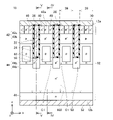
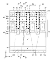
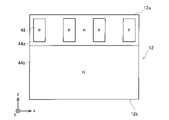
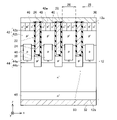
- FIG. 2 is a top plan view of the MOSFET according to the embodiment (with the source electrode and the interlayer insulating film omitted); Sectional drawing in the II-II line of FIG.1, 4, 5.
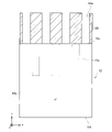
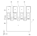
- Explanatory drawing of the manufacturing method of MOSFET (the top view which looked at the semiconductor substrate).
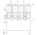
- FIG. 3 is an explanatory view of a method of manufacturing a MOSFET (cross-sectional view of a portion corresponding to FIG. 2);
- FIG. 3 is an explanatory view of a method of manufacturing a MOSFET (cross-sectional view of a portion corresponding to FIG. 2);
- FIG. 3 is an explanatory view of a method of manufacturing a MOSFET (cross-sectional view of a portion corresponding to FIG. 2);
- FIG. 3 is an explanatory view of a method of manufacturing a MOSFET (cross-sectional view of a portion corresponding to FIG. 2);
- FIG. 3 is an explanatory view of a method of manufacturing a MOSFET (cross-sectional view of a portion corresponding to FIG. 2);
- FIG. 3 is an explanatory view of a modified example of the manufacturing method of the MOSFET (cross-sectional view of a portion corresponding to FIG. 2);
- FIG. 3 is an explanatory view of a modified example of the manufacturing method of the MOSFET (cross-sectional view of a portion corresponding to FIG. 2);
- FIG. 3 is an explanatory view of a modified example of the manufacturing method of the MOSFET (cross-sectional view of a portion corresponding to FIG. 2);
- Sectional drawing corresponding to FIG. 2 of MOSFET of the modification 1 (sectional drawing of the location corresponding to FIG. 2).
- Sectional drawing corresponding to FIG. 2 of MOSFET of the modification 2 sectional drawing of the location corresponding to FIG. 2).
- Sectional drawing corresponding to FIG. 2 of MOSFET of the modification 3 sectional drawing of the location corresponding to FIG. 2).
- An example field effect transistor disclosed in this specification may further have a plurality of p-type bottom regions.
- Each of the bottom regions may have a lower p-type impurity concentration than each of the breakdown voltage regions.
- Each of the bottom regions may be in contact with the gate insulating film at the lower end of the corresponding trench and may be spaced apart from each of the breakdown voltage regions.
- the electric field concentration at the lower end of the trench can be more effectively suppressed by the bottom region.
- the drift region may have a low concentration region and a high concentration region having a higher n-type impurity concentration than the low concentration region.
- the high-concentration region is distributed from a position in contact with the body region to a position below the lower end of each trench, and is formed in each gate insulating film at a position between each breakdown voltage region and each gate insulating film. may be in contact with each other.
- the low concentration region may be in contact with the high concentration region from below.
- This specification proposes a method for manufacturing any of the above field effect transistors.
- This manufacturing method includes the steps of forming a mask extending in a grid pattern on the upper surface of the semiconductor substrate, and implanting a p-type impurity into the semiconductor substrate through the mask, thereby forming the plurality of breakdown voltage regions in the semiconductor substrate.
- a step of forming a mask extending in a grid pattern on the upper surface of the semiconductor substrate and implanting a p-type impurity into the semiconductor substrate through the mask, thereby forming the plurality of breakdown voltage regions in the semiconductor substrate.
- the mask since the mask is formed in a grid pattern, the mask can be stably formed. That is, it is possible to prevent the mask from partially falling down. Therefore, a field effect transistor can be suitably manufactured.
- the manufacturing method disclosed herein comprises the steps of forming a trench in the top surface of the semiconductor substrate, and implanting p-type impurities into the top surface of the semiconductor substrate and the bottom surface of the trench to form the body region and the bottom. It may further have a step of forming a region.
- the body region and the bottom region can be formed at the same time.
- MOSFET 10 metal oxide semiconductor field effect transistor
- MOSFET 10 has a semiconductor substrate 12 .
- the thickness direction of the semiconductor substrate 12 will be referred to as the z-direction
- one direction perpendicular to the z-direction will be referred to as the x-direction
- the direction perpendicular to the z-direction and the x-direction will be referred to as the y-direction.
- the x-direction and the y-direction are parallel to the upper surface 12a and the lower surface 12b of the semiconductor substrate 12, respectively.
- a plurality of trenches 20 are provided in the upper surface 12a of the semiconductor substrate 12. As shown in FIGS. As shown in FIG. 1, each trench 20 extends linearly in the y direction. The multiple trenches 20 are spaced apart in the x-direction. In the following, a range sandwiched between the plurality of trenches 20 in the interior of the semiconductor substrate 12 is referred to as an inter-trench range 28 .
- each trench 20 is covered with a gate insulating film 22 .
- a gate electrode 24 is disposed within each trench 20 .
- Each gate electrode 24 is insulated from the semiconductor substrate 12 by a gate insulating film 22 .
- An upper surface of each gate electrode 24 is covered with an interlayer insulating film 26 .
- the source electrode 30 is arranged on the upper surface 12a of the semiconductor substrate 12. As shown in FIGS. The source electrode 30 covers the interlayer insulating film 26 and the upper surface 12 a of the semiconductor substrate 12 . The source electrode 30 is in contact with the upper surface 12a of the semiconductor substrate 12 within a range where the interlayer insulating film 26 does not exist. The source electrode 30 is insulated from the gate electrode 24 by an interlayer insulating film 26 .
- a drain electrode 32 is arranged on the lower surface 12 b of the semiconductor substrate 12 .
- the drain electrode 32 is in contact with substantially the entire lower surface 12 b of the semiconductor substrate 12 .
- semiconductor substrate 12 includes a plurality of source regions 40, a body region 42, a drift region 44, a drain region 46, a plurality of breakdown voltage regions 48, and a plurality of bottom regions 50. As shown in FIGS. .
- each source region 40 is an n-type region and has a relatively high n-type impurity concentration.
- Each source region 40 is disposed within a corresponding inter-trench range 28 .
- Two source regions 40 are provided in each inter-trench area 28 .
- Each source region 40 is positioned adjacent to the corresponding trench 20 .
- each source region 40 extends along the trench 20 in the y direction.
- each source region 40 contacts the gate insulating film 22 at the upper end of the corresponding trench 20 .
- Each source region 40 is in ohmic contact with the source electrode 30 .
- the body region 42 is a p-type region. As shown in FIGS. 2 and 3, body region 42 extends across multiple inter-trench regions 28 .
- the body region 42 has a plurality of contact regions 42a and low concentration regions 42b. Each contact region 42a has a p-type impurity concentration higher than that of the low concentration region 42b.
- Each contact region 42a is disposed between two source regions 40 within a corresponding inter-trench area 28. As shown in FIG. Each contact region 42 a is in ohmic contact with the source electrode 30 . As shown in FIG. 1, each contact region 42a extends along the trench 20 in the y direction.
- the low-concentration regions 42b are distributed over a plurality of inter-trench ranges 28. As shown in FIGS.
- the lightly doped region 42b contacts the contact region 42a and the source region 40 from below within each inter-trench region 28 .
- the low-concentration region 42 b is in contact with the gate insulating film 22 below each source region 40
- the drift region 44 is an n-type region having a lower n-type impurity concentration than the source region 40. As shown in FIGS. 2 and 3, the drift region 44 is in contact with the body region 42 (more specifically, the low concentration region 42b) from below. The drift region 44 is in contact with the gate insulating film 22 below the body region 42 . Drift region 44 is separated from source region 40 by body region 42 . Drift regions 44 are distributed within each inter-trench area 28 to an area below each trench 20 . In the range below each trench 20, the drift regions 44 are widely distributed in the lateral direction.
- the drift region 44 has a high concentration region 44a and a low concentration region 44b. The high concentration region 44a has a higher n-type impurity concentration than the low concentration region 44b.
- the high-concentration region 44a is in contact with the body region 42 (more specifically, the low-concentration region 42b) from below.
- the high-concentration regions 44 a are distributed from a position in contact with the body region 42 to below the lower end of each trench 20 .
- the low-concentration region 44 b is arranged below the lower end of each trench 20 .
- the low concentration region 44b is in contact with the high concentration region 44a from below.
- the low-concentration regions 44b are widely distributed in the lateral direction across each range below each inter-trench range 28 .
- the drain region 46 is an n-type region with a higher n-type impurity concentration than the drift region 44 .
- the drain region 46 is in contact with the drift region 44 (more specifically, the low concentration region 44b) from below. Drain region 46 is arranged in a range including lower surface 12 b of semiconductor substrate 12 . Drain region 46 is in ohmic contact with drain electrode 32 .
- the multiple breakdown voltage regions 48 are p-type regions having a p-type impurity concentration higher than that of the body regions 42 . As shown in FIG. 2, each breakdown voltage region 48 is located within the corresponding inter-trench range 28 . Each breakdown voltage region 48 is arranged within a range surrounded by the drift region 44 (more specifically, the high concentration region 44a). As shown in FIG. 1, within each inter-trench range 28, a plurality of breakdown voltage regions 48 are provided. Within each inter-trench range 28, breakdown voltage regions 48 are spaced apart in the y-direction (ie, the direction parallel to trenches 20).
- a row 49 is formed by linearly arranging a plurality of breakdown voltage regions 48 arranged in different inter-trench ranges 28 along the x-direction (the direction intersecting with the plurality of trenches 20). Within each row 49, a plurality of breakdown voltage regions 48 are spaced apart in the x-direction. A plurality of rows 49 of breakdown voltage regions 48 (that is, rows extending in the x direction) are formed in the semiconductor substrate 12 . Each row 49 is spaced apart in the y-direction. As shown in FIG. 2 , each breakdown voltage region 48 extends from a position above the lower end of each trench 20 to a position below the lower end of each trench 20 . A space C1 is provided between each breakdown voltage region 48 and the gate insulating film 22 .
- each breakdown voltage region 48 is not in contact with the gate insulating film 22 .
- a drift region 44 (more specifically, a high-concentration region 44a) is arranged at the interval C1.
- the drift region 44 (more specifically, the high-concentration region 44a) is in contact with the gate insulating film 22 at the interval C1.
- Each breakdown voltage region 48 is isolated from the body region 42 .
- Each breakdown voltage region 48 floats within the drift region 44 .
- the drift region 44 (more specifically, the high-concentration region 44a) is in contact with the gate insulating film 22 below the body region 42 at the position where the breakdown voltage region 48 is not provided. .
- the plurality of bottom regions 50 are p-type regions having a p-type impurity concentration lower than that of the breakdown voltage region 48 .
- the p-type impurity concentration of each bottom region 50 is approximately equal to the p-type impurity concentration of the body region 42 .
- each bottom region 50 is located below the corresponding trench 20 .
- Each bottom region 50 contacts the gate insulating film 22 at the bottom surface of the corresponding trench 20 .
- the drift region 44 is in contact with the side and bottom surfaces of each bottom region 50 .
- Each bottom region 50 floats within drift region 44 .
- Each bottom region 50 extends from the lower end of each trench 20 to a depth reaching the low concentration region 44b. As shown in FIG.
- each bottom region 50 extends continuously along the trench 20 in the y-direction. Each bottom region 50 is in contact with the gate insulating film 22 over substantially the entire bottom surface of the corresponding trench 20 . As shown in FIG. 2, a space is provided between each bottom region 50 and the breakdown voltage region 48 . Therefore, each bottom region 50 does not contact the breakdown voltage region 48 .
- a channel is formed in the body region 42 in the vicinity of the gate insulating film 22 when a potential equal to or higher than the threshold is applied to the gate electrode 24 .
- a potential higher than that of the source electrode 30 is applied to the drain electrode 32 with the channel formed, electrons flow from the source region 40 to the drain region 46 via the channel and the drift region 44 . That is, the MOSFET 10 is turned on.
- the cross section shown in FIG. 3 where the breakdown voltage region 48 does not exist electrons that have passed through the channel flow downward in the drift region 44 as indicated by arrows 102 .
- the breakdown voltage region 48 is not in contact with the gate insulating film 22 below the body region 42, so that electrons passing through the channel are emitted as indicated by arrows 100 in FIG. It flows downward through the drift region 44 within the interval C1.
- the p-type breakdown voltage region 48 is not in contact with the gate insulating film 22, electrons passing through the channel can flow downward along the side surfaces of the trench 20. Therefore, the ON resistance of this MOSFET 10 is low.
- a depletion layer with a very small width extends from the breakdown voltage region 48 and the bottom region 50 (that is, the p-type region) into the drift region 44 .
- the breakdown voltage region 48 is located away from the gate insulation film 22 , the depletion layer extending from the breakdown voltage region 48 into the drift region 44 does not reach the gate insulation film 22 . Therefore, the depletion layer extending from the breakdown voltage region 48 into the drift region 44 inhibits the flow of electrons. Also, since the p-type impurity concentration of the bottom region 50 is low, the width of the depletion layer extending from the bottom region 50 into the drift region 44 is extremely small.
- the depletion layer extending from the bottom region 50 into the drift region 44 is less likely to block the flow of electrons, so the on-resistance of the MOSFET 10 is further reduced.
- the drift region 44 around the breakdown voltage region 48 is composed of the high concentration region 44a. Since the n-type impurity concentration of the high concentration region 44a is high, the resistivity of the high concentration region 44a is low. Therefore, electrons that have passed through the channel can flow through the high-concentration region 44a with low loss. In particular, since the drift region 44 in the narrow space C1 is composed of the high-concentration region 44a, electrons can pass through the space C1 with low loss. This further reduces the ON resistance of the MOSFET 10 .
- the MOSFET 10 When the potential of the gate electrode 24 is lowered to a value less than that, the channel disappears and the flow of electrons stops. That is, the MOSFET 10 is turned off. When the MOSFET 10 is turned off, a depletion layer spreads from the body region 42 to the drift region 44, and the drift region 44 is depleted over a wide range. At this time, a depletion layer widely extends from the breakdown voltage region 48 and the bottom region 50 to the drift region 44 as well. Withstand voltage region 48 is arranged at a position away from the lower end of trench 20 .
- the depletion layer extending from the breakdown voltage region 48 extends to the periphery of the lower end of the trench 20 .
- the drift region 44 is depleted around the bottom end of the trench 20 by the depletion layer extending from the breakdown voltage region 48 , thereby suppressing electric field concentration at the bottom end of the trench 20 .
- the drift region 44 around the lower end of the trench 20 is also depleted by the depletion layer extending from the bottom region 50 . This also suppresses electric field concentration at the lower end of the trench 20 .
- the depletion layer spreads from the breakdown voltage region 48 and the bottom region 50 to the vicinity of the lower end of the trench 20, so that electric field concentration at the lower end of the trench 20 is suppressed.
- the breakdown voltage region 48 with a high p-type impurity concentration is less likely to be depleted when the MOSFET 10 is turned off. Since the withstand voltage region 48, which is difficult to deplete, extends from the top to the bottom of the lower end of the trench 20, when the MOSFET 10 is turned off, an electric field is less likely to occur in the drift region 44 in the range above the lower end of the withstand voltage region 48. 4 and 6, the presence of the breakdown voltage region 48 makes it difficult for equipotential lines to enter the drift region 44 above the lower end of the breakdown voltage region 48 . This also suppresses electric field concentration at the lower end of the trench 20 .
- MOSFET 10 of the embodiment electric field concentration at the lower end of the trench 20 is suppressed. Therefore, application of a high electric field to gate insulating film 22 at the lower end of trench 20 is suppressed. Therefore, MOSFET 10 has a high withstand voltage.
- the breakdown voltage region 48 does not exist around the trench 20 in the MOSFET 10 of the embodiment. Therefore, the volume of the breakdown voltage region 48 is smaller than that of a conventional MOSFET in which the breakdown voltage region extends continuously in the direction intersecting the trench.
- the volume of the breakdown voltage region at the intersection is relatively small. Therefore, even if the breakdown voltage region 48 is eliminated at the crossing portion as in the MOSFET 10 of the embodiment, the reduction in volume of the breakdown voltage region 48 is small. Therefore, in the MOSFET 10 of the embodiment, a sufficient volume of the breakdown voltage region 48 can be secured, and a depletion layer can be widely extended from the breakdown voltage region 48 into the drift region 44 when the MOSFET 10 is turned off.
- the MOSFET 10 of the embodiment can reduce the on-resistance while maintaining a high breakdown voltage.
- the entire semiconductor substrate 12 before processing is composed of the low-concentration region 44 b of the drift region 44 .
- a mask 80 is formed on the upper surface 12a of the semiconductor substrate 12. As shown in FIG. Here, the mask 80 is formed so that the opening 80a is arranged above the range in which the withstand voltage region 48 is to be formed. In other words, a grid-like mask 80 is formed so as to avoid the area where the breakdown voltage region 48 should be formed.
- the beam portion of the mask 80 extending in the y direction extends along the range 20x in which the trench 20 is to be formed, and the beam portion of the mask 80 extending in the x direction extends in a direction perpendicular to the range 20x in which the trench 20 is to be formed.
- p-type impurities are implanted into the semiconductor substrate 12 through the mask 80 .
- the implantation energy is increased to implant the p-type impurity from the upper surface 12a to a deep position.
- a plurality of withstand voltage regions 48 are formed.
- the mask 80 is removed.
- the mask 80 needs to be thick because the ion implantation process for the withstand voltage region 48 uses high implantation energy as described above. Therefore, the cross-sectional shape of the mask 80 has a high aspect ratio as shown in FIGS. In general, forming a mask with such a high aspect ratio may cause partial collapse of the mask. However, in this embodiment, since the mask 80 is formed in a grid pattern as shown in FIG. 7, the collapse of the mask 80 is prevented.
- a mask (not shown) is formed to cover the outer periphery of the MOSFET 10, and n-type impurity ions are implanted into the semiconductor substrate 12 through the mask as shown in FIG. As a result, a high concentration region 44a is formed in the semiconductor substrate 12. Next, as shown in FIG.
- trenches 20 are formed by selectively etching the upper surface 12a of the semiconductor substrate 12. Then, as shown in FIG. 11, trenches 20 are formed by selectively etching the upper surface 12a of the semiconductor substrate 12. Then, as shown in FIG.
- p-type impurities are implanted into the semiconductor substrate 12 from the upper surface 12a side. Thereby, the low concentration region 42b of the body region 42 is formed. At this time, the p-type impurity is also implanted into the bottom surface of the trench 20 . As a result, a p-type bottom region 50 is formed in the range exposed at the bottom of trench 20 . Thus, in this manufacturing method, the low concentration region 42b and the bottom region 50 can be formed at the same time.
- a gate insulating film 22 and a gate electrode 24 are formed inside the trench 20 .
- a contact region 42a, a source region 40, and a drain region 46 are formed by ion implantation.
- the interlayer insulating film 26, the source electrode 30, and the drain electrode 32 are formed to complete the MOSFET 10 shown in FIGS.
- the low-concentration region 42b of the body region 42 is formed by ion implantation in the manufacturing method described above, the low-concentration region 42b may be formed by epitaxial growth.
- the high-concentration region 44a of the withstanding region 48 and the drift region 44 is formed by ion implantation in a shallow range near the upper surface 12a of the semiconductor substrate 12.
- FIG. 14 a low concentration region 42b is epitaxially grown on the semiconductor substrate 12.
- trenches 20 and bottom regions 50 are formed.
- MOSFET 10 is thus completed.
- the breakdown voltage region 48 may be formed by ion implantation after forming the trench 20 .
- the lower end of the withstand voltage region 48 is located above the lower end of the high concentration region 44a.
- the breakdown voltage region 48 may reach the low concentration region 44b.
- the withstand voltage region 48 is separated from the body region 42 .
- the breakdown voltage region 48 may be connected to the body region 42.
- the bottom region 50 is provided below the trench 20 .
- bottom region 50 may not be provided below trench 20 .
- the depletion layer extending from the breakdown voltage region 48 can suppress electric field concentration at the lower end of the trench 20 .
- the drift region 44 has the high-concentration region 44a and the low-concentration region 44b.
- the n-type impurity concentration may be uniform throughout the drift region 44 .
Landscapes
- Insulated Gate Type Field-Effect Transistor (AREA)
- Chemical & Material Sciences (AREA)
- Composite Materials (AREA)
Priority Applications (2)
| Application Number | Priority Date | Filing Date | Title |
|---|---|---|---|
| CN202280032568.4A CN117242582A (zh) | 2021-06-11 | 2022-01-18 | 场效应晶体管及其制造方法 |
| US18/461,679 US12557350B2 (en) | 2021-06-11 | 2023-09-06 | Field-effect transistor and method for manufacturing same |
Applications Claiming Priority (2)
| Application Number | Priority Date | Filing Date | Title |
|---|---|---|---|
| JP2021-098031 | 2021-06-11 | ||
| JP2021098031A JP7615904B2 (ja) | 2021-06-11 | 2021-06-11 | 電界効果トランジスタとその製造方法 |
Related Child Applications (1)
| Application Number | Title | Priority Date | Filing Date |
|---|---|---|---|
| US18/461,679 Continuation US12557350B2 (en) | 2021-06-11 | 2023-09-06 | Field-effect transistor and method for manufacturing same |
Publications (1)
| Publication Number | Publication Date |
|---|---|
| WO2022259593A1 true WO2022259593A1 (ja) | 2022-12-15 |
Family
ID=84425611
Family Applications (1)
| Application Number | Title | Priority Date | Filing Date |
|---|---|---|---|
| PCT/JP2022/001571 Ceased WO2022259593A1 (ja) | 2021-06-11 | 2022-01-18 | 電界効果トランジスタとその製造方法 |
Country Status (4)
| Country | Link |
|---|---|
| US (1) | US12557350B2 (https=) |
| JP (1) | JP7615904B2 (https=) |
| CN (1) | CN117242582A (https=) |
| WO (1) | WO2022259593A1 (https=) |
Families Citing this family (1)
| Publication number | Priority date | Publication date | Assignee | Title |
|---|---|---|---|---|
| JP7717010B2 (ja) * | 2022-03-08 | 2025-08-01 | 株式会社デンソー | 半導体装置 |
Citations (4)
| Publication number | Priority date | Publication date | Assignee | Title |
|---|---|---|---|---|
| JP2011253837A (ja) * | 2010-05-31 | 2011-12-15 | Denso Corp | 炭化珪素半導体装置およびその製造方法 |
| JP2020155739A (ja) * | 2019-03-22 | 2020-09-24 | 富士電機株式会社 | 絶縁ゲート型半導体装置 |
| JP2020191401A (ja) * | 2019-05-23 | 2020-11-26 | 富士電機株式会社 | 半導体装置及び半導体装置の製造方法 |
| JP2021068741A (ja) * | 2019-10-18 | 2021-04-30 | 富士電機株式会社 | 半導体装置 |
Family Cites Families (12)
| Publication number | Priority date | Publication date | Assignee | Title |
|---|---|---|---|---|
| GB0403934D0 (en) | 2004-02-21 | 2004-03-24 | Koninkl Philips Electronics Nv | Trench-gate semiconductor devices and the manufacture thereof |
| CN100502041C (zh) * | 2005-04-28 | 2009-06-17 | 恩益禧电子股份有限公司 | 半导体器件 |
| JP5196980B2 (ja) * | 2007-12-10 | 2013-05-15 | 株式会社東芝 | 半導体装置 |
| EP2091083A3 (en) | 2008-02-13 | 2009-10-14 | Denso Corporation | Silicon carbide semiconductor device including a deep layer |
| JP6283468B2 (ja) | 2013-03-01 | 2018-02-21 | 株式会社豊田中央研究所 | 逆導通igbt |
| JP2014236171A (ja) | 2013-06-05 | 2014-12-15 | ローム株式会社 | 半導体装置およびその製造方法 |
| JP2015195262A (ja) | 2014-03-31 | 2015-11-05 | マイクロン テクノロジー, インク. | 半導体装置及びその製造方法 |
| JP6255111B2 (ja) * | 2014-09-17 | 2017-12-27 | 株式会社日立製作所 | 半導体装置、インバータモジュール、インバータ、鉄道車両、および半導体装置の製造方法 |
| CN105977302A (zh) * | 2016-07-06 | 2016-09-28 | 电子科技大学 | 一种具有埋层结构的槽栅型mos |
| JP2019087611A (ja) | 2017-11-06 | 2019-06-06 | トヨタ自動車株式会社 | スイッチング素子とその製造方法 |
| JP7052330B2 (ja) * | 2017-12-13 | 2022-04-12 | 富士電機株式会社 | 絶縁ゲート型半導体装置及びその製造方法 |
| JP7622449B2 (ja) * | 2021-01-22 | 2025-01-28 | 富士電機株式会社 | 半導体装置 |
-
2021
- 2021-06-11 JP JP2021098031A patent/JP7615904B2/ja active Active
-
2022
- 2022-01-18 WO PCT/JP2022/001571 patent/WO2022259593A1/ja not_active Ceased
- 2022-01-18 CN CN202280032568.4A patent/CN117242582A/zh active Pending
-
2023
- 2023-09-06 US US18/461,679 patent/US12557350B2/en active Active
Patent Citations (4)
| Publication number | Priority date | Publication date | Assignee | Title |
|---|---|---|---|---|
| JP2011253837A (ja) * | 2010-05-31 | 2011-12-15 | Denso Corp | 炭化珪素半導体装置およびその製造方法 |
| JP2020155739A (ja) * | 2019-03-22 | 2020-09-24 | 富士電機株式会社 | 絶縁ゲート型半導体装置 |
| JP2020191401A (ja) * | 2019-05-23 | 2020-11-26 | 富士電機株式会社 | 半導体装置及び半導体装置の製造方法 |
| JP2021068741A (ja) * | 2019-10-18 | 2021-04-30 | 富士電機株式会社 | 半導体装置 |
Also Published As
| Publication number | Publication date |
|---|---|
| CN117242582A (zh) | 2023-12-15 |
| JP2022189453A (ja) | 2022-12-22 |
| US12557350B2 (en) | 2026-02-17 |
| JP7615904B2 (ja) | 2025-01-17 |
| US20230411449A1 (en) | 2023-12-21 |
Similar Documents
| Publication | Publication Date | Title |
|---|---|---|
| TWI553861B (zh) | High withstand voltage semiconductor device | |
| KR101864889B1 (ko) | 수평형 디모스 트랜지스터 및 그 제조방법 | |
| US8735249B2 (en) | Trenched power semiconductor device and fabrication method thereof | |
| US11437510B2 (en) | Trench MOSFET and method of manufacturing trench MOSFET | |
| JP2019087611A (ja) | スイッチング素子とその製造方法 | |
| JP4998524B2 (ja) | 半導体装置 | |
| JP7651403B2 (ja) | 電界効果トランジスタとその製造方法 | |
| JP7717900B2 (ja) | 半導体装置 | |
| US12205983B2 (en) | Semiconductor device and manufacturing method of semiconductor device | |
| CN117099213A (zh) | 半导体装置及其制造方法 | |
| US20230246102A1 (en) | Superjunction semiconductor device | |
| US11251299B2 (en) | Silicon carbide semiconductor device and manufacturing method of same | |
| US10319851B2 (en) | Semiconductor device and method for manufacturing same | |
| JP2017191817A (ja) | スイッチング素子の製造方法 | |
| US20230369483A1 (en) | Semiconductor device and manufacturing method of semiconductor device | |
| US12557350B2 (en) | Field-effect transistor and method for manufacturing same | |
| US20250120142A1 (en) | Semiconductor device and manufacturing method of semiconductor device | |
| JP2012204379A (ja) | 電力用半導体装置 | |
| JP2024137200A (ja) | 電界効果トランジスタ | |
| CN117581382A (zh) | 半导体装置和半导体装置的制造方法 | |
| JP7852457B2 (ja) | 半導体装置とその製造方法 | |
| US20250254935A1 (en) | Semiconductor device | |
| JP7230477B2 (ja) | トレンチゲート型のスイッチング素子の製造方法 | |
| CN112652666B (zh) | 一种功率半导体器件及其制作方法 | |
| CN120302682A (zh) | 场效应晶体管及其制造方法 |
Legal Events
| Date | Code | Title | Description |
|---|---|---|---|
| 121 | Ep: the epo has been informed by wipo that ep was designated in this application |
Ref document number: 22819784 Country of ref document: EP Kind code of ref document: A1 |
|
| WWE | Wipo information: entry into national phase |
Ref document number: 202280032568.4 Country of ref document: CN |
|
| NENP | Non-entry into the national phase |
Ref country code: DE |
|
| 122 | Ep: pct application non-entry in european phase |
Ref document number: 22819784 Country of ref document: EP Kind code of ref document: A1 |