WO2022259593A1 - Field-effect transistor and method for manufacturing same - Google Patents
Field-effect transistor and method for manufacturing same Download PDFInfo
- Publication number
- WO2022259593A1 WO2022259593A1 PCT/JP2022/001571 JP2022001571W WO2022259593A1 WO 2022259593 A1 WO2022259593 A1 WO 2022259593A1 JP 2022001571 W JP2022001571 W JP 2022001571W WO 2022259593 A1 WO2022259593 A1 WO 2022259593A1
- Authority
- WO
- WIPO (PCT)
- Prior art keywords
- region
- trench
- gate insulating
- breakdown voltage
- insulating film
- Prior art date
Links
- 230000005669 field effect Effects 0.000 title claims abstract description 23
- 238000004519 manufacturing process Methods 0.000 title claims description 21
- 238000000034 method Methods 0.000 title claims description 7
- 230000015556 catabolic process Effects 0.000 claims abstract description 73
- 239000004065 semiconductor Substances 0.000 claims abstract description 44
- 239000000758 substrate Substances 0.000 claims abstract description 43
- 210000000746 body region Anatomy 0.000 claims description 38
- 239000012535 impurity Substances 0.000 claims description 30
- 239000012212 insulator Substances 0.000 abstract 1
- 239000010410 layer Substances 0.000 description 25
- 230000005684 electric field Effects 0.000 description 14
- 239000011229 interlayer Substances 0.000 description 7
- 238000005468 ion implantation Methods 0.000 description 5
- 230000004048 modification Effects 0.000 description 4
- 238000012986 modification Methods 0.000 description 4
- 238000002513 implantation Methods 0.000 description 2
- 238000009413 insulation Methods 0.000 description 2
- 238000009826 distribution Methods 0.000 description 1
- 238000005530 etching Methods 0.000 description 1
- 239000007943 implant Substances 0.000 description 1
- 150000002500 ions Chemical class 0.000 description 1
- 238000002955 isolation Methods 0.000 description 1
- 229910044991 metal oxide Inorganic materials 0.000 description 1
- 150000004706 metal oxides Chemical class 0.000 description 1
Images


Classifications
-
- H—ELECTRICITY
- H01—ELECTRIC ELEMENTS
- H01L—SEMICONDUCTOR DEVICES NOT COVERED BY CLASS H10
- H01L29/00—Semiconductor devices adapted for rectifying, amplifying, oscillating or switching, or capacitors or resistors with at least one potential-jump barrier or surface barrier, e.g. PN junction depletion layer or carrier concentration layer; Details of semiconductor bodies or of electrodes thereof ; Multistep manufacturing processes therefor
- H01L29/02—Semiconductor bodies ; Multistep manufacturing processes therefor
- H01L29/06—Semiconductor bodies ; Multistep manufacturing processes therefor characterised by their shape; characterised by the shapes, relative sizes, or dispositions of the semiconductor regions ; characterised by the concentration or distribution of impurities within semiconductor regions
- H01L29/0603—Semiconductor bodies ; Multistep manufacturing processes therefor characterised by their shape; characterised by the shapes, relative sizes, or dispositions of the semiconductor regions ; characterised by the concentration or distribution of impurities within semiconductor regions characterised by particular constructional design considerations, e.g. for preventing surface leakage, for controlling electric field concentration or for internal isolations regions
- H01L29/0607—Semiconductor bodies ; Multistep manufacturing processes therefor characterised by their shape; characterised by the shapes, relative sizes, or dispositions of the semiconductor regions ; characterised by the concentration or distribution of impurities within semiconductor regions characterised by particular constructional design considerations, e.g. for preventing surface leakage, for controlling electric field concentration or for internal isolations regions for preventing surface leakage or controlling electric field concentration
- H01L29/0611—Semiconductor bodies ; Multistep manufacturing processes therefor characterised by their shape; characterised by the shapes, relative sizes, or dispositions of the semiconductor regions ; characterised by the concentration or distribution of impurities within semiconductor regions characterised by particular constructional design considerations, e.g. for preventing surface leakage, for controlling electric field concentration or for internal isolations regions for preventing surface leakage or controlling electric field concentration for increasing or controlling the breakdown voltage of reverse biased devices
- H01L29/0615—Semiconductor bodies ; Multistep manufacturing processes therefor characterised by their shape; characterised by the shapes, relative sizes, or dispositions of the semiconductor regions ; characterised by the concentration or distribution of impurities within semiconductor regions characterised by particular constructional design considerations, e.g. for preventing surface leakage, for controlling electric field concentration or for internal isolations regions for preventing surface leakage or controlling electric field concentration for increasing or controlling the breakdown voltage of reverse biased devices by the doping profile or the shape or the arrangement of the PN junction, or with supplementary regions, e.g. junction termination extension [JTE]
- H01L29/063—Reduced surface field [RESURF] pn-junction structures
- H01L29/0634—Multiple reduced surface field (multi-RESURF) structures, e.g. double RESURF, charge compensation, cool, superjunction (SJ), 3D-RESURF, composite buffer (CB) structures
-
- H—ELECTRICITY
- H01—ELECTRIC ELEMENTS
- H01L—SEMICONDUCTOR DEVICES NOT COVERED BY CLASS H10
- H01L21/00—Processes or apparatus adapted for the manufacture or treatment of semiconductor or solid state devices or of parts thereof
- H01L21/02—Manufacture or treatment of semiconductor devices or of parts thereof
- H01L21/04—Manufacture or treatment of semiconductor devices or of parts thereof the devices having at least one potential-jump barrier or surface barrier, e.g. PN junction, depletion layer or carrier concentration layer
- H01L21/18—Manufacture or treatment of semiconductor devices or of parts thereof the devices having at least one potential-jump barrier or surface barrier, e.g. PN junction, depletion layer or carrier concentration layer the devices having semiconductor bodies comprising elements of Group IV of the Periodic System or AIIIBV compounds with or without impurities, e.g. doping materials
- H01L21/26—Bombardment with radiation
- H01L21/263—Bombardment with radiation with high-energy radiation
- H01L21/265—Bombardment with radiation with high-energy radiation producing ion implantation
- H01L21/26506—Bombardment with radiation with high-energy radiation producing ion implantation in group IV semiconductors
- H01L21/26513—Bombardment with radiation with high-energy radiation producing ion implantation in group IV semiconductors of electrically active species
-
- H—ELECTRICITY
- H01—ELECTRIC ELEMENTS
- H01L—SEMICONDUCTOR DEVICES NOT COVERED BY CLASS H10
- H01L21/00—Processes or apparatus adapted for the manufacture or treatment of semiconductor or solid state devices or of parts thereof
- H01L21/02—Manufacture or treatment of semiconductor devices or of parts thereof
- H01L21/04—Manufacture or treatment of semiconductor devices or of parts thereof the devices having at least one potential-jump barrier or surface barrier, e.g. PN junction, depletion layer or carrier concentration layer
- H01L21/18—Manufacture or treatment of semiconductor devices or of parts thereof the devices having at least one potential-jump barrier or surface barrier, e.g. PN junction, depletion layer or carrier concentration layer the devices having semiconductor bodies comprising elements of Group IV of the Periodic System or AIIIBV compounds with or without impurities, e.g. doping materials
- H01L21/26—Bombardment with radiation
- H01L21/263—Bombardment with radiation with high-energy radiation
- H01L21/265—Bombardment with radiation with high-energy radiation producing ion implantation
- H01L21/266—Bombardment with radiation with high-energy radiation producing ion implantation using masks
-
- H—ELECTRICITY
- H01—ELECTRIC ELEMENTS
- H01L—SEMICONDUCTOR DEVICES NOT COVERED BY CLASS H10
- H01L29/00—Semiconductor devices adapted for rectifying, amplifying, oscillating or switching, or capacitors or resistors with at least one potential-jump barrier or surface barrier, e.g. PN junction depletion layer or carrier concentration layer; Details of semiconductor bodies or of electrodes thereof ; Multistep manufacturing processes therefor
- H01L29/02—Semiconductor bodies ; Multistep manufacturing processes therefor
- H01L29/06—Semiconductor bodies ; Multistep manufacturing processes therefor characterised by their shape; characterised by the shapes, relative sizes, or dispositions of the semiconductor regions ; characterised by the concentration or distribution of impurities within semiconductor regions
- H01L29/0603—Semiconductor bodies ; Multistep manufacturing processes therefor characterised by their shape; characterised by the shapes, relative sizes, or dispositions of the semiconductor regions ; characterised by the concentration or distribution of impurities within semiconductor regions characterised by particular constructional design considerations, e.g. for preventing surface leakage, for controlling electric field concentration or for internal isolations regions
- H01L29/0607—Semiconductor bodies ; Multistep manufacturing processes therefor characterised by their shape; characterised by the shapes, relative sizes, or dispositions of the semiconductor regions ; characterised by the concentration or distribution of impurities within semiconductor regions characterised by particular constructional design considerations, e.g. for preventing surface leakage, for controlling electric field concentration or for internal isolations regions for preventing surface leakage or controlling electric field concentration
- H01L29/0611—Semiconductor bodies ; Multistep manufacturing processes therefor characterised by their shape; characterised by the shapes, relative sizes, or dispositions of the semiconductor regions ; characterised by the concentration or distribution of impurities within semiconductor regions characterised by particular constructional design considerations, e.g. for preventing surface leakage, for controlling electric field concentration or for internal isolations regions for preventing surface leakage or controlling electric field concentration for increasing or controlling the breakdown voltage of reverse biased devices
- H01L29/0615—Semiconductor bodies ; Multistep manufacturing processes therefor characterised by their shape; characterised by the shapes, relative sizes, or dispositions of the semiconductor regions ; characterised by the concentration or distribution of impurities within semiconductor regions characterised by particular constructional design considerations, e.g. for preventing surface leakage, for controlling electric field concentration or for internal isolations regions for preventing surface leakage or controlling electric field concentration for increasing or controlling the breakdown voltage of reverse biased devices by the doping profile or the shape or the arrangement of the PN junction, or with supplementary regions, e.g. junction termination extension [JTE]
- H01L29/0619—Semiconductor bodies ; Multistep manufacturing processes therefor characterised by their shape; characterised by the shapes, relative sizes, or dispositions of the semiconductor regions ; characterised by the concentration or distribution of impurities within semiconductor regions characterised by particular constructional design considerations, e.g. for preventing surface leakage, for controlling electric field concentration or for internal isolations regions for preventing surface leakage or controlling electric field concentration for increasing or controlling the breakdown voltage of reverse biased devices by the doping profile or the shape or the arrangement of the PN junction, or with supplementary regions, e.g. junction termination extension [JTE] with a supplementary region doped oppositely to or in rectifying contact with the semiconductor containing or contacting region, e.g. guard rings with PN or Schottky junction
- H01L29/0623—Buried supplementary region, e.g. buried guard ring
-
- H—ELECTRICITY
- H01—ELECTRIC ELEMENTS
- H01L—SEMICONDUCTOR DEVICES NOT COVERED BY CLASS H10
- H01L29/00—Semiconductor devices adapted for rectifying, amplifying, oscillating or switching, or capacitors or resistors with at least one potential-jump barrier or surface barrier, e.g. PN junction depletion layer or carrier concentration layer; Details of semiconductor bodies or of electrodes thereof ; Multistep manufacturing processes therefor
- H01L29/02—Semiconductor bodies ; Multistep manufacturing processes therefor
- H01L29/06—Semiconductor bodies ; Multistep manufacturing processes therefor characterised by their shape; characterised by the shapes, relative sizes, or dispositions of the semiconductor regions ; characterised by the concentration or distribution of impurities within semiconductor regions
- H01L29/0684—Semiconductor bodies ; Multistep manufacturing processes therefor characterised by their shape; characterised by the shapes, relative sizes, or dispositions of the semiconductor regions ; characterised by the concentration or distribution of impurities within semiconductor regions characterised by the shape, relative sizes or dispositions of the semiconductor regions or junctions between the regions
- H01L29/0692—Surface layout
- H01L29/0696—Surface layout of cellular field-effect devices, e.g. multicellular DMOS transistors or IGBTs
-
- H—ELECTRICITY
- H01—ELECTRIC ELEMENTS
- H01L—SEMICONDUCTOR DEVICES NOT COVERED BY CLASS H10
- H01L29/00—Semiconductor devices adapted for rectifying, amplifying, oscillating or switching, or capacitors or resistors with at least one potential-jump barrier or surface barrier, e.g. PN junction depletion layer or carrier concentration layer; Details of semiconductor bodies or of electrodes thereof ; Multistep manufacturing processes therefor
- H01L29/02—Semiconductor bodies ; Multistep manufacturing processes therefor
- H01L29/06—Semiconductor bodies ; Multistep manufacturing processes therefor characterised by their shape; characterised by the shapes, relative sizes, or dispositions of the semiconductor regions ; characterised by the concentration or distribution of impurities within semiconductor regions
- H01L29/08—Semiconductor bodies ; Multistep manufacturing processes therefor characterised by their shape; characterised by the shapes, relative sizes, or dispositions of the semiconductor regions ; characterised by the concentration or distribution of impurities within semiconductor regions with semiconductor regions connected to an electrode carrying current to be rectified, amplified or switched and such electrode being part of a semiconductor device which comprises three or more electrodes
- H01L29/0843—Source or drain regions of field-effect devices
- H01L29/0847—Source or drain regions of field-effect devices of field-effect transistors with insulated gate
- H01L29/0852—Source or drain regions of field-effect devices of field-effect transistors with insulated gate of DMOS transistors
- H01L29/0873—Drain regions
- H01L29/0878—Impurity concentration or distribution
-
- H—ELECTRICITY
- H01—ELECTRIC ELEMENTS
- H01L—SEMICONDUCTOR DEVICES NOT COVERED BY CLASS H10
- H01L29/00—Semiconductor devices adapted for rectifying, amplifying, oscillating or switching, or capacitors or resistors with at least one potential-jump barrier or surface barrier, e.g. PN junction depletion layer or carrier concentration layer; Details of semiconductor bodies or of electrodes thereof ; Multistep manufacturing processes therefor
- H01L29/02—Semiconductor bodies ; Multistep manufacturing processes therefor
- H01L29/06—Semiconductor bodies ; Multistep manufacturing processes therefor characterised by their shape; characterised by the shapes, relative sizes, or dispositions of the semiconductor regions ; characterised by the concentration or distribution of impurities within semiconductor regions
- H01L29/10—Semiconductor bodies ; Multistep manufacturing processes therefor characterised by their shape; characterised by the shapes, relative sizes, or dispositions of the semiconductor regions ; characterised by the concentration or distribution of impurities within semiconductor regions with semiconductor regions connected to an electrode not carrying current to be rectified, amplified or switched and such electrode being part of a semiconductor device which comprises three or more electrodes
- H01L29/1095—Body region, i.e. base region, of DMOS transistors or IGBTs
-
- H—ELECTRICITY
- H01—ELECTRIC ELEMENTS
- H01L—SEMICONDUCTOR DEVICES NOT COVERED BY CLASS H10
- H01L29/00—Semiconductor devices adapted for rectifying, amplifying, oscillating or switching, or capacitors or resistors with at least one potential-jump barrier or surface barrier, e.g. PN junction depletion layer or carrier concentration layer; Details of semiconductor bodies or of electrodes thereof ; Multistep manufacturing processes therefor
- H01L29/02—Semiconductor bodies ; Multistep manufacturing processes therefor
- H01L29/12—Semiconductor bodies ; Multistep manufacturing processes therefor characterised by the materials of which they are formed
- H01L29/16—Semiconductor bodies ; Multistep manufacturing processes therefor characterised by the materials of which they are formed including, apart from doping materials or other impurities, only elements of Group IV of the Periodic System
- H01L29/1608—Silicon carbide
-
- H—ELECTRICITY
- H01—ELECTRIC ELEMENTS
- H01L—SEMICONDUCTOR DEVICES NOT COVERED BY CLASS H10
- H01L29/00—Semiconductor devices adapted for rectifying, amplifying, oscillating or switching, or capacitors or resistors with at least one potential-jump barrier or surface barrier, e.g. PN junction depletion layer or carrier concentration layer; Details of semiconductor bodies or of electrodes thereof ; Multistep manufacturing processes therefor
- H01L29/66—Types of semiconductor device ; Multistep manufacturing processes therefor
- H01L29/66007—Multistep manufacturing processes
- H01L29/66053—Multistep manufacturing processes of devices having a semiconductor body comprising crystalline silicon carbide
- H01L29/66068—Multistep manufacturing processes of devices having a semiconductor body comprising crystalline silicon carbide the devices being controllable only by the electric current supplied or the electric potential applied, to an electrode which does not carry the current to be rectified, amplified or switched, e.g. three-terminal devices
-
- H—ELECTRICITY
- H01—ELECTRIC ELEMENTS
- H01L—SEMICONDUCTOR DEVICES NOT COVERED BY CLASS H10
- H01L29/00—Semiconductor devices adapted for rectifying, amplifying, oscillating or switching, or capacitors or resistors with at least one potential-jump barrier or surface barrier, e.g. PN junction depletion layer or carrier concentration layer; Details of semiconductor bodies or of electrodes thereof ; Multistep manufacturing processes therefor
- H01L29/66—Types of semiconductor device ; Multistep manufacturing processes therefor
- H01L29/66007—Multistep manufacturing processes
- H01L29/66075—Multistep manufacturing processes of devices having semiconductor bodies comprising group 14 or group 13/15 materials
- H01L29/66227—Multistep manufacturing processes of devices having semiconductor bodies comprising group 14 or group 13/15 materials the devices being controllable only by the electric current supplied or the electric potential applied, to an electrode which does not carry the current to be rectified, amplified or switched, e.g. three-terminal devices
- H01L29/66409—Unipolar field-effect transistors
- H01L29/66477—Unipolar field-effect transistors with an insulated gate, i.e. MISFET
- H01L29/66674—DMOS transistors, i.e. MISFETs with a channel accommodating body or base region adjoining a drain drift region
- H01L29/66712—Vertical DMOS transistors, i.e. VDMOS transistors
- H01L29/66734—Vertical DMOS transistors, i.e. VDMOS transistors with a step of recessing the gate electrode, e.g. to form a trench gate electrode
-
- H—ELECTRICITY
- H01—ELECTRIC ELEMENTS
- H01L—SEMICONDUCTOR DEVICES NOT COVERED BY CLASS H10
- H01L29/00—Semiconductor devices adapted for rectifying, amplifying, oscillating or switching, or capacitors or resistors with at least one potential-jump barrier or surface barrier, e.g. PN junction depletion layer or carrier concentration layer; Details of semiconductor bodies or of electrodes thereof ; Multistep manufacturing processes therefor
- H01L29/66—Types of semiconductor device ; Multistep manufacturing processes therefor
- H01L29/68—Types of semiconductor device ; Multistep manufacturing processes therefor controllable by only the electric current supplied, or only the electric potential applied, to an electrode which does not carry the current to be rectified, amplified or switched
- H01L29/76—Unipolar devices, e.g. field effect transistors
- H01L29/772—Field effect transistors
- H01L29/78—Field effect transistors with field effect produced by an insulated gate
- H01L29/7801—DMOS transistors, i.e. MISFETs with a channel accommodating body or base region adjoining a drain drift region
- H01L29/7802—Vertical DMOS transistors, i.e. VDMOS transistors
- H01L29/7813—Vertical DMOS transistors, i.e. VDMOS transistors with trench gate electrode, e.g. UMOS transistors
Definitions
- the technology disclosed in this specification relates to field effect transistors.
- Patent Document 1 The field effect transistor disclosed in Japanese Patent Publication No. 2009-194065 (hereinafter referred to as Patent Document 1) has a plurality of p-type deep layers protruding downward from the body region. Each deep layer extends along a direction transverse to each trench. Each deep layer is spaced apart in a direction parallel to each trench. Each deep layer extends from above the lower end of each trench to below the lower end of each trench. According to this configuration, the depletion layer extends from each deep layer to the drift region, thereby suppressing electric field concentration at the lower end of each trench. Thereby, the gate insulating film can be protected from the electric field at the lower end of each trench.
- each deep layer is in contact with the side surface of the trench (that is, the gate insulating film) below the body region. Therefore, electrons that have passed through the channel formed in the body region cannot flow from the body region into the underlying deep layer. That is, electrons bypass the deep layer and flow into the drift region. Therefore, the field effect transistor of Patent Document 1 has a problem of high ON voltage.
- This specification proposes a field effect transistor capable of suppressing the electric field concentration at the lower end of the trench and reducing the ON voltage.
- a field effect transistor disclosed in the present specification includes a semiconductor substrate having a plurality of trenches provided on an upper surface thereof, a gate insulating film covering inner surfaces of the trenches, and a gate insulating film disposed in the trenches, the gate insulating film forming the a gate electrode insulated from the semiconductor substrate;
- the semiconductor substrate has a plurality of n-type source regions, a p-type body region, an n-type drift region, and a plurality of p-type breakdown regions.
- Each area of the semiconductor substrate located between the plurality of trenches is an inter-trench area.
- Each of the plurality of source regions is provided within the range between the corresponding trenches and is in contact with the corresponding gate insulating film.
- the body region extends across the inter-trench regions and contacts the gate insulating films below the source regions in the inter-trench regions.
- the drift region is distributed over a range from the inter-trench region to the range below the trenches, and is in contact with the gate insulating films below the body region.
- a plurality of the withstand voltage regions are provided within the range between the trenches.
- a plurality of the withstand voltage regions are arranged to form a plurality of columns extending along a first direction intersecting the plurality of trenches. Within each column, a plurality of the withstand voltage regions are arranged at intervals in the first direction. A plurality of said columns are spaced apart in a second direction parallel to said trenches.
- Each of the breakdown voltage regions has a higher p-type impurity concentration than the body region, extends from above a bottom edge of each trench to below the bottom edge of each trench, and is spaced from each gate isolation. are placed open.
- the drift region is in contact with the gate insulating film at a position between each breakdown voltage region and each gate insulating film.
- a p-type breakdown voltage region extends from above the lower end of each trench to below the lower end of each trench at a position spaced apart from each gate insulating film.
- a depletion layer extends from each breakdown voltage region into the drift region.
- Each withstand voltage region is arranged at a position spaced apart from each gate insulating film, but since the p-type impurity concentration of each withstand voltage region is high, a depletion layer can extend from each withstand voltage region to the periphery of the bottom end of the trench. . Therefore, electric field concentration at the lower end of each trench is suppressed, and the gate insulating film is protected from the electric field.
- the drift region is in contact with the gate insulating film at a position between each breakdown voltage region and each gate insulating film. Therefore, when this field effect transistor is turned on, electrons passing through the channel formed in the body region can flow into the drift region without being blocked by the breakdown voltage region. Therefore, this field effect transistor has a low on-resistance.
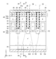
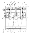
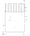
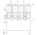
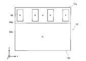
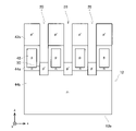
- FIG. 2 is a top plan view of the MOSFET according to the embodiment (with the source electrode and the interlayer insulating film omitted); Sectional drawing in the II-II line of FIG.1, 4, 5.
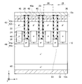
- Explanatory drawing of the manufacturing method of MOSFET (the top view which looked at the semiconductor substrate).
- FIG. 3 is an explanatory view of a method of manufacturing a MOSFET (cross-sectional view of a portion corresponding to FIG. 2);
- FIG. 3 is an explanatory view of a method of manufacturing a MOSFET (cross-sectional view of a portion corresponding to FIG. 2);
- FIG. 3 is an explanatory view of a method of manufacturing a MOSFET (cross-sectional view of a portion corresponding to FIG. 2);
- FIG. 3 is an explanatory view of a method of manufacturing a MOSFET (cross-sectional view of a portion corresponding to FIG. 2);
- FIG. 3 is an explanatory view of a method of manufacturing a MOSFET (cross-sectional view of a portion corresponding to FIG. 2);
- FIG. 3 is an explanatory view of a modified example of the manufacturing method of the MOSFET (cross-sectional view of a portion corresponding to FIG. 2);
- FIG. 3 is an explanatory view of a modified example of the manufacturing method of the MOSFET (cross-sectional view of a portion corresponding to FIG. 2);
- FIG. 3 is an explanatory view of a modified example of the manufacturing method of the MOSFET (cross-sectional view of a portion corresponding to FIG. 2);
- Sectional drawing corresponding to FIG. 2 of MOSFET of the modification 1 (sectional drawing of the location corresponding to FIG. 2).
- Sectional drawing corresponding to FIG. 2 of MOSFET of the modification 2 sectional drawing of the location corresponding to FIG. 2).
- Sectional drawing corresponding to FIG. 2 of MOSFET of the modification 3 sectional drawing of the location corresponding to FIG. 2).
- An example field effect transistor disclosed in this specification may further have a plurality of p-type bottom regions.
- Each of the bottom regions may have a lower p-type impurity concentration than each of the breakdown voltage regions.
- Each of the bottom regions may be in contact with the gate insulating film at the lower end of the corresponding trench and may be spaced apart from each of the breakdown voltage regions.
- the electric field concentration at the lower end of the trench can be more effectively suppressed by the bottom region.
- the drift region may have a low concentration region and a high concentration region having a higher n-type impurity concentration than the low concentration region.
- the high-concentration region is distributed from a position in contact with the body region to a position below the lower end of each trench, and is formed in each gate insulating film at a position between each breakdown voltage region and each gate insulating film. may be in contact with each other.
- the low concentration region may be in contact with the high concentration region from below.
- This specification proposes a method for manufacturing any of the above field effect transistors.
- This manufacturing method includes the steps of forming a mask extending in a grid pattern on the upper surface of the semiconductor substrate, and implanting a p-type impurity into the semiconductor substrate through the mask, thereby forming the plurality of breakdown voltage regions in the semiconductor substrate.
- a step of forming a mask extending in a grid pattern on the upper surface of the semiconductor substrate and implanting a p-type impurity into the semiconductor substrate through the mask, thereby forming the plurality of breakdown voltage regions in the semiconductor substrate.
- the mask since the mask is formed in a grid pattern, the mask can be stably formed. That is, it is possible to prevent the mask from partially falling down. Therefore, a field effect transistor can be suitably manufactured.
- the manufacturing method disclosed herein comprises the steps of forming a trench in the top surface of the semiconductor substrate, and implanting p-type impurities into the top surface of the semiconductor substrate and the bottom surface of the trench to form the body region and the bottom. It may further have a step of forming a region.
- the body region and the bottom region can be formed at the same time.
- MOSFET 10 metal oxide semiconductor field effect transistor
- MOSFET 10 has a semiconductor substrate 12 .
- the thickness direction of the semiconductor substrate 12 will be referred to as the z-direction
- one direction perpendicular to the z-direction will be referred to as the x-direction
- the direction perpendicular to the z-direction and the x-direction will be referred to as the y-direction.
- the x-direction and the y-direction are parallel to the upper surface 12a and the lower surface 12b of the semiconductor substrate 12, respectively.
- a plurality of trenches 20 are provided in the upper surface 12a of the semiconductor substrate 12. As shown in FIGS. As shown in FIG. 1, each trench 20 extends linearly in the y direction. The multiple trenches 20 are spaced apart in the x-direction. In the following, a range sandwiched between the plurality of trenches 20 in the interior of the semiconductor substrate 12 is referred to as an inter-trench range 28 .
- each trench 20 is covered with a gate insulating film 22 .
- a gate electrode 24 is disposed within each trench 20 .
- Each gate electrode 24 is insulated from the semiconductor substrate 12 by a gate insulating film 22 .
- An upper surface of each gate electrode 24 is covered with an interlayer insulating film 26 .
- the source electrode 30 is arranged on the upper surface 12a of the semiconductor substrate 12. As shown in FIGS. The source electrode 30 covers the interlayer insulating film 26 and the upper surface 12 a of the semiconductor substrate 12 . The source electrode 30 is in contact with the upper surface 12a of the semiconductor substrate 12 within a range where the interlayer insulating film 26 does not exist. The source electrode 30 is insulated from the gate electrode 24 by an interlayer insulating film 26 .
- a drain electrode 32 is arranged on the lower surface 12 b of the semiconductor substrate 12 .
- the drain electrode 32 is in contact with substantially the entire lower surface 12 b of the semiconductor substrate 12 .
- semiconductor substrate 12 includes a plurality of source regions 40, a body region 42, a drift region 44, a drain region 46, a plurality of breakdown voltage regions 48, and a plurality of bottom regions 50. As shown in FIGS. .
- each source region 40 is an n-type region and has a relatively high n-type impurity concentration.
- Each source region 40 is disposed within a corresponding inter-trench range 28 .
- Two source regions 40 are provided in each inter-trench area 28 .
- Each source region 40 is positioned adjacent to the corresponding trench 20 .
- each source region 40 extends along the trench 20 in the y direction.
- each source region 40 contacts the gate insulating film 22 at the upper end of the corresponding trench 20 .
- Each source region 40 is in ohmic contact with the source electrode 30 .
- the body region 42 is a p-type region. As shown in FIGS. 2 and 3, body region 42 extends across multiple inter-trench regions 28 .
- the body region 42 has a plurality of contact regions 42a and low concentration regions 42b. Each contact region 42a has a p-type impurity concentration higher than that of the low concentration region 42b.
- Each contact region 42a is disposed between two source regions 40 within a corresponding inter-trench area 28. As shown in FIG. Each contact region 42 a is in ohmic contact with the source electrode 30 . As shown in FIG. 1, each contact region 42a extends along the trench 20 in the y direction.
- the low-concentration regions 42b are distributed over a plurality of inter-trench ranges 28. As shown in FIGS.
- the lightly doped region 42b contacts the contact region 42a and the source region 40 from below within each inter-trench region 28 .
- the low-concentration region 42 b is in contact with the gate insulating film 22 below each source region 40
- the drift region 44 is an n-type region having a lower n-type impurity concentration than the source region 40. As shown in FIGS. 2 and 3, the drift region 44 is in contact with the body region 42 (more specifically, the low concentration region 42b) from below. The drift region 44 is in contact with the gate insulating film 22 below the body region 42 . Drift region 44 is separated from source region 40 by body region 42 . Drift regions 44 are distributed within each inter-trench area 28 to an area below each trench 20 . In the range below each trench 20, the drift regions 44 are widely distributed in the lateral direction.
- the drift region 44 has a high concentration region 44a and a low concentration region 44b. The high concentration region 44a has a higher n-type impurity concentration than the low concentration region 44b.
- the high-concentration region 44a is in contact with the body region 42 (more specifically, the low-concentration region 42b) from below.
- the high-concentration regions 44 a are distributed from a position in contact with the body region 42 to below the lower end of each trench 20 .
- the low-concentration region 44 b is arranged below the lower end of each trench 20 .
- the low concentration region 44b is in contact with the high concentration region 44a from below.
- the low-concentration regions 44b are widely distributed in the lateral direction across each range below each inter-trench range 28 .
- the drain region 46 is an n-type region with a higher n-type impurity concentration than the drift region 44 .
- the drain region 46 is in contact with the drift region 44 (more specifically, the low concentration region 44b) from below. Drain region 46 is arranged in a range including lower surface 12 b of semiconductor substrate 12 . Drain region 46 is in ohmic contact with drain electrode 32 .
- the multiple breakdown voltage regions 48 are p-type regions having a p-type impurity concentration higher than that of the body regions 42 . As shown in FIG. 2, each breakdown voltage region 48 is located within the corresponding inter-trench range 28 . Each breakdown voltage region 48 is arranged within a range surrounded by the drift region 44 (more specifically, the high concentration region 44a). As shown in FIG. 1, within each inter-trench range 28, a plurality of breakdown voltage regions 48 are provided. Within each inter-trench range 28, breakdown voltage regions 48 are spaced apart in the y-direction (ie, the direction parallel to trenches 20).
- a row 49 is formed by linearly arranging a plurality of breakdown voltage regions 48 arranged in different inter-trench ranges 28 along the x-direction (the direction intersecting with the plurality of trenches 20). Within each row 49, a plurality of breakdown voltage regions 48 are spaced apart in the x-direction. A plurality of rows 49 of breakdown voltage regions 48 (that is, rows extending in the x direction) are formed in the semiconductor substrate 12 . Each row 49 is spaced apart in the y-direction. As shown in FIG. 2 , each breakdown voltage region 48 extends from a position above the lower end of each trench 20 to a position below the lower end of each trench 20 . A space C1 is provided between each breakdown voltage region 48 and the gate insulating film 22 .
- each breakdown voltage region 48 is not in contact with the gate insulating film 22 .
- a drift region 44 (more specifically, a high-concentration region 44a) is arranged at the interval C1.
- the drift region 44 (more specifically, the high-concentration region 44a) is in contact with the gate insulating film 22 at the interval C1.
- Each breakdown voltage region 48 is isolated from the body region 42 .
- Each breakdown voltage region 48 floats within the drift region 44 .
- the drift region 44 (more specifically, the high-concentration region 44a) is in contact with the gate insulating film 22 below the body region 42 at the position where the breakdown voltage region 48 is not provided. .
- the plurality of bottom regions 50 are p-type regions having a p-type impurity concentration lower than that of the breakdown voltage region 48 .
- the p-type impurity concentration of each bottom region 50 is approximately equal to the p-type impurity concentration of the body region 42 .
- each bottom region 50 is located below the corresponding trench 20 .
- Each bottom region 50 contacts the gate insulating film 22 at the bottom surface of the corresponding trench 20 .
- the drift region 44 is in contact with the side and bottom surfaces of each bottom region 50 .
- Each bottom region 50 floats within drift region 44 .
- Each bottom region 50 extends from the lower end of each trench 20 to a depth reaching the low concentration region 44b. As shown in FIG.
- each bottom region 50 extends continuously along the trench 20 in the y-direction. Each bottom region 50 is in contact with the gate insulating film 22 over substantially the entire bottom surface of the corresponding trench 20 . As shown in FIG. 2, a space is provided between each bottom region 50 and the breakdown voltage region 48 . Therefore, each bottom region 50 does not contact the breakdown voltage region 48 .
- a channel is formed in the body region 42 in the vicinity of the gate insulating film 22 when a potential equal to or higher than the threshold is applied to the gate electrode 24 .
- a potential higher than that of the source electrode 30 is applied to the drain electrode 32 with the channel formed, electrons flow from the source region 40 to the drain region 46 via the channel and the drift region 44 . That is, the MOSFET 10 is turned on.
- the cross section shown in FIG. 3 where the breakdown voltage region 48 does not exist electrons that have passed through the channel flow downward in the drift region 44 as indicated by arrows 102 .
- the breakdown voltage region 48 is not in contact with the gate insulating film 22 below the body region 42, so that electrons passing through the channel are emitted as indicated by arrows 100 in FIG. It flows downward through the drift region 44 within the interval C1.
- the p-type breakdown voltage region 48 is not in contact with the gate insulating film 22, electrons passing through the channel can flow downward along the side surfaces of the trench 20. Therefore, the ON resistance of this MOSFET 10 is low.
- a depletion layer with a very small width extends from the breakdown voltage region 48 and the bottom region 50 (that is, the p-type region) into the drift region 44 .
- the breakdown voltage region 48 is located away from the gate insulation film 22 , the depletion layer extending from the breakdown voltage region 48 into the drift region 44 does not reach the gate insulation film 22 . Therefore, the depletion layer extending from the breakdown voltage region 48 into the drift region 44 inhibits the flow of electrons. Also, since the p-type impurity concentration of the bottom region 50 is low, the width of the depletion layer extending from the bottom region 50 into the drift region 44 is extremely small.
- the depletion layer extending from the bottom region 50 into the drift region 44 is less likely to block the flow of electrons, so the on-resistance of the MOSFET 10 is further reduced.
- the drift region 44 around the breakdown voltage region 48 is composed of the high concentration region 44a. Since the n-type impurity concentration of the high concentration region 44a is high, the resistivity of the high concentration region 44a is low. Therefore, electrons that have passed through the channel can flow through the high-concentration region 44a with low loss. In particular, since the drift region 44 in the narrow space C1 is composed of the high-concentration region 44a, electrons can pass through the space C1 with low loss. This further reduces the ON resistance of the MOSFET 10 .
- the MOSFET 10 When the potential of the gate electrode 24 is lowered to a value less than that, the channel disappears and the flow of electrons stops. That is, the MOSFET 10 is turned off. When the MOSFET 10 is turned off, a depletion layer spreads from the body region 42 to the drift region 44, and the drift region 44 is depleted over a wide range. At this time, a depletion layer widely extends from the breakdown voltage region 48 and the bottom region 50 to the drift region 44 as well. Withstand voltage region 48 is arranged at a position away from the lower end of trench 20 .
- the depletion layer extending from the breakdown voltage region 48 extends to the periphery of the lower end of the trench 20 .
- the drift region 44 is depleted around the bottom end of the trench 20 by the depletion layer extending from the breakdown voltage region 48 , thereby suppressing electric field concentration at the bottom end of the trench 20 .
- the drift region 44 around the lower end of the trench 20 is also depleted by the depletion layer extending from the bottom region 50 . This also suppresses electric field concentration at the lower end of the trench 20 .
- the depletion layer spreads from the breakdown voltage region 48 and the bottom region 50 to the vicinity of the lower end of the trench 20, so that electric field concentration at the lower end of the trench 20 is suppressed.
- the breakdown voltage region 48 with a high p-type impurity concentration is less likely to be depleted when the MOSFET 10 is turned off. Since the withstand voltage region 48, which is difficult to deplete, extends from the top to the bottom of the lower end of the trench 20, when the MOSFET 10 is turned off, an electric field is less likely to occur in the drift region 44 in the range above the lower end of the withstand voltage region 48. 4 and 6, the presence of the breakdown voltage region 48 makes it difficult for equipotential lines to enter the drift region 44 above the lower end of the breakdown voltage region 48 . This also suppresses electric field concentration at the lower end of the trench 20 .
- MOSFET 10 of the embodiment electric field concentration at the lower end of the trench 20 is suppressed. Therefore, application of a high electric field to gate insulating film 22 at the lower end of trench 20 is suppressed. Therefore, MOSFET 10 has a high withstand voltage.
- the breakdown voltage region 48 does not exist around the trench 20 in the MOSFET 10 of the embodiment. Therefore, the volume of the breakdown voltage region 48 is smaller than that of a conventional MOSFET in which the breakdown voltage region extends continuously in the direction intersecting the trench.
- the volume of the breakdown voltage region at the intersection is relatively small. Therefore, even if the breakdown voltage region 48 is eliminated at the crossing portion as in the MOSFET 10 of the embodiment, the reduction in volume of the breakdown voltage region 48 is small. Therefore, in the MOSFET 10 of the embodiment, a sufficient volume of the breakdown voltage region 48 can be secured, and a depletion layer can be widely extended from the breakdown voltage region 48 into the drift region 44 when the MOSFET 10 is turned off.
- the MOSFET 10 of the embodiment can reduce the on-resistance while maintaining a high breakdown voltage.
- the entire semiconductor substrate 12 before processing is composed of the low-concentration region 44 b of the drift region 44 .
- a mask 80 is formed on the upper surface 12a of the semiconductor substrate 12. As shown in FIG. Here, the mask 80 is formed so that the opening 80a is arranged above the range in which the withstand voltage region 48 is to be formed. In other words, a grid-like mask 80 is formed so as to avoid the area where the breakdown voltage region 48 should be formed.
- the beam portion of the mask 80 extending in the y direction extends along the range 20x in which the trench 20 is to be formed, and the beam portion of the mask 80 extending in the x direction extends in a direction perpendicular to the range 20x in which the trench 20 is to be formed.
- p-type impurities are implanted into the semiconductor substrate 12 through the mask 80 .
- the implantation energy is increased to implant the p-type impurity from the upper surface 12a to a deep position.
- a plurality of withstand voltage regions 48 are formed.
- the mask 80 is removed.
- the mask 80 needs to be thick because the ion implantation process for the withstand voltage region 48 uses high implantation energy as described above. Therefore, the cross-sectional shape of the mask 80 has a high aspect ratio as shown in FIGS. In general, forming a mask with such a high aspect ratio may cause partial collapse of the mask. However, in this embodiment, since the mask 80 is formed in a grid pattern as shown in FIG. 7, the collapse of the mask 80 is prevented.
- a mask (not shown) is formed to cover the outer periphery of the MOSFET 10, and n-type impurity ions are implanted into the semiconductor substrate 12 through the mask as shown in FIG. As a result, a high concentration region 44a is formed in the semiconductor substrate 12. Next, as shown in FIG.
- trenches 20 are formed by selectively etching the upper surface 12a of the semiconductor substrate 12. Then, as shown in FIG. 11, trenches 20 are formed by selectively etching the upper surface 12a of the semiconductor substrate 12. Then, as shown in FIG.
- p-type impurities are implanted into the semiconductor substrate 12 from the upper surface 12a side. Thereby, the low concentration region 42b of the body region 42 is formed. At this time, the p-type impurity is also implanted into the bottom surface of the trench 20 . As a result, a p-type bottom region 50 is formed in the range exposed at the bottom of trench 20 . Thus, in this manufacturing method, the low concentration region 42b and the bottom region 50 can be formed at the same time.
- a gate insulating film 22 and a gate electrode 24 are formed inside the trench 20 .
- a contact region 42a, a source region 40, and a drain region 46 are formed by ion implantation.
- the interlayer insulating film 26, the source electrode 30, and the drain electrode 32 are formed to complete the MOSFET 10 shown in FIGS.
- the low-concentration region 42b of the body region 42 is formed by ion implantation in the manufacturing method described above, the low-concentration region 42b may be formed by epitaxial growth.
- the high-concentration region 44a of the withstanding region 48 and the drift region 44 is formed by ion implantation in a shallow range near the upper surface 12a of the semiconductor substrate 12.
- FIG. 14 a low concentration region 42b is epitaxially grown on the semiconductor substrate 12.
- trenches 20 and bottom regions 50 are formed.
- MOSFET 10 is thus completed.
- the breakdown voltage region 48 may be formed by ion implantation after forming the trench 20 .
- the lower end of the withstand voltage region 48 is located above the lower end of the high concentration region 44a.
- the breakdown voltage region 48 may reach the low concentration region 44b.
- the withstand voltage region 48 is separated from the body region 42 .
- the breakdown voltage region 48 may be connected to the body region 42.
- the bottom region 50 is provided below the trench 20 .
- bottom region 50 may not be provided below trench 20 .
- the depletion layer extending from the breakdown voltage region 48 can suppress electric field concentration at the lower end of the trench 20 .
- the drift region 44 has the high-concentration region 44a and the low-concentration region 44b.
- the n-type impurity concentration may be uniform throughout the drift region 44 .
Abstract
Provided is a field-effect transistor that has a semiconductor substrate (12) that is provided with a plurality of trenches (20) in an upper surface, and gate electrodes (24) that are arranged in the trenches. A plurality of breakdown voltage areas (48) are provided in each inter-trench range (28). The plurality of breakdown voltage areas are arranged so as to form a plurality of rows (49) extending in a first direction that intersects the plurality of trenches. The plurality of rows are arranged spaced apart in a second direction that is parallel to the trenches. The breakdown voltage areas extend from above the lower ends of the trenches to below the lower ends of the trenches, and are arranged spaced apart from gate insulators (22). The drift areas are in contact with the gate insulating films at positions between the breakdown voltage areas and the gate insulating films.
Description
(関連出願の相互参照)
本出願は、2021年6月11日に出願された日本特許出願特願2021-098031の関連出願であり、この日本特許出願に基づく優先権を主張するものであり、この日本特許出願に記載された全ての内容を、本明細書を構成するものとして援用する。 (Cross reference to related applications)
This application is a related application of Japanese Patent Application No. 2021-098031 filed on June 11, 2021, and claims priority based on this Japanese patent application. , the entire contents of which are incorporated herein by reference.
本明細書に開示の技術は、電界効果トランジスタに関する。
The technology disclosed in this specification relates to field effect transistors.
日本特許公開2009-194065号(以下、特許文献1という)に開示の電界効果トランジスタは、ボディ領域から下側に向かって突出するp型の複数のディープ層を有している。各ディープ層は、各トレンチに対して交差する方向に沿って伸びている。各ディープ層は、各トレンチに平行な方向に間隔を開けて配置されている。各ディープ層は、各トレンチの下端よりも上側から各トレンチの下端よりも下側まで伸びている。この構成によれば、各ディープ層からドリフト領域に空乏層が伸びることで、各トレンチの下端における電界集中が抑制される。これにより、各トレンチの下端においてゲート絶縁膜を電界から保護することができる。
The field effect transistor disclosed in Japanese Patent Publication No. 2009-194065 (hereinafter referred to as Patent Document 1) has a plurality of p-type deep layers protruding downward from the body region. Each deep layer extends along a direction transverse to each trench. Each deep layer is spaced apart in a direction parallel to each trench. Each deep layer extends from above the lower end of each trench to below the lower end of each trench. According to this configuration, the depletion layer extends from each deep layer to the drift region, thereby suppressing electric field concentration at the lower end of each trench. Thereby, the gate insulating film can be protected from the electric field at the lower end of each trench.
特許文献1の電界効果トランジスタでは、ボディ領域の下側において各ディープ層がトレンチの側面(すなわち、ゲート絶縁膜)に接している。このため、ボディ領域に形成されたチャネルを通過した電子が、ボディ領域からその下側のディープ層に流入することができない。すなわち、電子は、ディープ層を迂回してドリフト領域へ流れる。このため、特許文献1の電界効果トランジスタは、オン電圧が高いという問題を有している。本明細書では、トレンチの下端における電界集中を抑制できるとともに、オン電圧を低減できる電界効果トランジスタを提案する。
In the field effect transistor of Patent Document 1, each deep layer is in contact with the side surface of the trench (that is, the gate insulating film) below the body region. Therefore, electrons that have passed through the channel formed in the body region cannot flow from the body region into the underlying deep layer. That is, electrons bypass the deep layer and flow into the drift region. Therefore, the field effect transistor of Patent Document 1 has a problem of high ON voltage. This specification proposes a field effect transistor capable of suppressing the electric field concentration at the lower end of the trench and reducing the ON voltage.
本明細書が開示する電界効果トランジスタは、上面に複数のトレンチが設けられた半導体基板と、前記トレンチの内面を覆うゲート絶縁膜と、前記トレンチ内に配置されており、前記ゲート絶縁膜によって前記半導体基板から絶縁されたゲート電極、を有している。前記半導体基板が、複数のn型のソース領域と、p型のボディ領域と、n型のドリフト領域と、複数のp型の耐圧領域、を有する。前記半導体基板のうちの複数の前記トレンチの間に位置する各範囲がトレンチ間範囲である。複数の前記ソース領域のそれぞれが、対応する前記トレンチ間範囲内に設けられており、対応する前記ゲート絶縁膜に接している。前記ボディ領域が、前記各トレンチ間範囲に跨って伸びており、前記各トレンチ間範囲内において前記ソース領域の下側で前記各ゲート絶縁膜に接している。前記ドリフト領域が、前記各トレンチ間範囲域内から前記各トレンチよりも下側の範囲に跨って分布しており、前記ボディ領域の下側で前記各ゲート絶縁膜に接している。複数の前記耐圧領域が、前記各トレンチ間範囲内に設けられている。複数の前記耐圧領域が、複数の前記トレンチと交差する第1方向に沿って伸びる列を複数個構成するように配置されている。前記各列内において、複数の前記耐圧領域が前記第1方向に間隔を開けて配置されている。複数の前記列が、前記トレンチと平行な第2方向に間隔を開けて配置されている。前記各耐圧領域が、前記ボディ領域よりも高いp型不純物濃度を有し、前記各トレンチの下端よりも上側から前記各トレンチの前記下端よりも下側まで伸びており、前記各ゲート絶縁から間隔を開けて配置されている。前記ドリフト領域が、前記各耐圧領域と前記各ゲート絶縁膜の間の位置で前記ゲート絶縁膜に接している。
A field effect transistor disclosed in the present specification includes a semiconductor substrate having a plurality of trenches provided on an upper surface thereof, a gate insulating film covering inner surfaces of the trenches, and a gate insulating film disposed in the trenches, the gate insulating film forming the a gate electrode insulated from the semiconductor substrate; The semiconductor substrate has a plurality of n-type source regions, a p-type body region, an n-type drift region, and a plurality of p-type breakdown regions. Each area of the semiconductor substrate located between the plurality of trenches is an inter-trench area. Each of the plurality of source regions is provided within the range between the corresponding trenches and is in contact with the corresponding gate insulating film. The body region extends across the inter-trench regions and contacts the gate insulating films below the source regions in the inter-trench regions. The drift region is distributed over a range from the inter-trench region to the range below the trenches, and is in contact with the gate insulating films below the body region. A plurality of the withstand voltage regions are provided within the range between the trenches. A plurality of the withstand voltage regions are arranged to form a plurality of columns extending along a first direction intersecting the plurality of trenches. Within each column, a plurality of the withstand voltage regions are arranged at intervals in the first direction. A plurality of said columns are spaced apart in a second direction parallel to said trenches. Each of the breakdown voltage regions has a higher p-type impurity concentration than the body region, extends from above a bottom edge of each trench to below the bottom edge of each trench, and is spaced from each gate isolation. are placed open. The drift region is in contact with the gate insulating film at a position between each breakdown voltage region and each gate insulating film.
この電界効果トランジスタでは、p型の耐圧領域が、各ゲート絶縁膜から間隔を開けた位置において、各トレンチの下端よりも上側から各トレンチの下端よりも下側まで伸びている。この電界効果トランジスタがオフすると、各耐圧領域からドリフト領域内に空乏層が伸びる。各耐圧領域は各ゲート絶縁膜から間隔を開けた位置に配置されているが、各耐圧領域のp型不純物濃度が高いので、各耐圧領域からトレンチの下端の周辺まで空乏層が伸びることができる。したがって、各トレンチの下端における電界集中が抑制され、ゲート絶縁膜が電界から保護される。また、この電界効果トランジスタでは、ドリフト領域が、各耐圧領域と各ゲート絶縁膜の間の位置でゲート絶縁膜に接している。したがって、この電界効果トランジスタがオンすると、ボディ領域に形成されたチャネルを通過した電子が、耐圧領域に阻害されることなくドリフト領域へ流れることができる。したがって、この電界効果トランジスタは、低いオン抵抗を有する。
In this field effect transistor, a p-type breakdown voltage region extends from above the lower end of each trench to below the lower end of each trench at a position spaced apart from each gate insulating film. When the field effect transistor is turned off, a depletion layer extends from each breakdown voltage region into the drift region. Each withstand voltage region is arranged at a position spaced apart from each gate insulating film, but since the p-type impurity concentration of each withstand voltage region is high, a depletion layer can extend from each withstand voltage region to the periphery of the bottom end of the trench. . Therefore, electric field concentration at the lower end of each trench is suppressed, and the gate insulating film is protected from the electric field. Also, in this field effect transistor, the drift region is in contact with the gate insulating film at a position between each breakdown voltage region and each gate insulating film. Therefore, when this field effect transistor is turned on, electrons passing through the channel formed in the body region can flow into the drift region without being blocked by the breakdown voltage region. Therefore, this field effect transistor has a low on-resistance.
本明細書が開示する一例の電界効果トランジスタは、複数のp型の底部領域をさらに有していてもよい。前記各底部領域が、前記各耐圧領域よりも低いp型不純物濃度を有していてもよい。前記各底部領域が、対応する前記トレンチの前記下端において前記ゲート絶縁膜に接しており、前記各耐圧領域から間隔を開けて配置されていてもよい。
An example field effect transistor disclosed in this specification may further have a plurality of p-type bottom regions. Each of the bottom regions may have a lower p-type impurity concentration than each of the breakdown voltage regions. Each of the bottom regions may be in contact with the gate insulating film at the lower end of the corresponding trench and may be spaced apart from each of the breakdown voltage regions.
この構成によれば、底部領域によってトレンチの下端における電界集中をより効果的に抑制することができる。
According to this configuration, the electric field concentration at the lower end of the trench can be more effectively suppressed by the bottom region.
本明細書が開示する一例の電界効果トランジスタでは、前記ドリフト領域が、低濃度領域と、前記低濃度領域よりもn型不純物濃度が高い高濃度領域を有していてもよい。前記高濃度領域が、前記ボディ領域に接する位置から前記各トレンチの前記下端よりも下側まで分布しており、前記各耐圧領域と前記各ゲート絶縁膜の間の位置で前記各ゲート絶縁膜に接していてもよい。前記低濃度領域が、前記高濃度領域に対して下側から接していてもよい。
In one example of the field effect transistor disclosed in this specification, the drift region may have a low concentration region and a high concentration region having a higher n-type impurity concentration than the low concentration region. The high-concentration region is distributed from a position in contact with the body region to a position below the lower end of each trench, and is formed in each gate insulating film at a position between each breakdown voltage region and each gate insulating film. may be in contact with each other. The low concentration region may be in contact with the high concentration region from below.
本明細書は、上記のいずれかの電界効果トランジスタの製造方法を提案する。この製造方法は、前記半導体基板の上面に格子状に伸びるマスクを形成する工程と、前記マスクを介して前記半導体基板にp型不純物を注入することによって、前記半導体基板内に複数の前記耐圧領域を形成する工程、を有していてもよい。
This specification proposes a method for manufacturing any of the above field effect transistors. This manufacturing method includes the steps of forming a mask extending in a grid pattern on the upper surface of the semiconductor substrate, and implanting a p-type impurity into the semiconductor substrate through the mask, thereby forming the plurality of breakdown voltage regions in the semiconductor substrate. A step of forming a
この構成によれば、マスクを格子状に形成するため、マスクを安定して形成することができる。すなわち、マスクが部分的に倒れることを抑制できる。したがって、電界効果トランジスタを好適に製造することができる。
According to this configuration, since the mask is formed in a grid pattern, the mask can be stably formed. That is, it is possible to prevent the mask from partially falling down. Therefore, a field effect transistor can be suitably manufactured.
本明細書が開示する製造方法は、前記半導体基板の前記上面にトレンチを形成する工程と、前記半導体基板の前記上面と前記トレンチの底面にp型不純物を注入することによって前記ボディ領域と前記底部領域を形成する工程をさらに有していてもよい。
The manufacturing method disclosed herein comprises the steps of forming a trench in the top surface of the semiconductor substrate, and implanting p-type impurities into the top surface of the semiconductor substrate and the bottom surface of the trench to form the body region and the bottom. It may further have a step of forming a region.
この製造方法によれば、ボディ領域と底部領域を同時に形成することができる。
According to this manufacturing method, the body region and the bottom region can be formed at the same time.
図1~5は、実施例のMOSFET10(metal oxide semiconductor field effect transistor)を示している。MOSFET10は、半導体基板12を有している。なお、以下では、半導体基板12の厚み方向をz方向といい、z方向に直交する一方向をx方向といい、z方向及びx方向に直交する方向をy方向という。x方向及びy方向は、半導体基板12の上面12a及び下面12bと平行である。
1 to 5 show the MOSFET 10 (metal oxide semiconductor field effect transistor) of the embodiment. MOSFET 10 has a semiconductor substrate 12 . Hereinafter, the thickness direction of the semiconductor substrate 12 will be referred to as the z-direction, one direction perpendicular to the z-direction will be referred to as the x-direction, and the direction perpendicular to the z-direction and the x-direction will be referred to as the y-direction. The x-direction and the y-direction are parallel to the upper surface 12a and the lower surface 12b of the semiconductor substrate 12, respectively.
図1~3に示すように、半導体基板12の上面12aに、複数のトレンチ20が設けられている。図1に示すように、各トレンチ20は、y方向に直線状に伸びている。複数のトレンチ20は、x方向に間隔を開けて配置されている。以下では、半導体基板12の内部のうち、複数のトレンチ20によって挟まれた範囲をトレンチ間範囲28という。
As shown in FIGS. 1 to 3, a plurality of trenches 20 are provided in the upper surface 12a of the semiconductor substrate 12. As shown in FIGS. As shown in FIG. 1, each trench 20 extends linearly in the y direction. The multiple trenches 20 are spaced apart in the x-direction. In the following, a range sandwiched between the plurality of trenches 20 in the interior of the semiconductor substrate 12 is referred to as an inter-trench range 28 .
各トレンチ20の内面は、ゲート絶縁膜22によって覆われている。各トレンチ20内に、ゲート電極24が配置されている。各ゲート電極24は、ゲート絶縁膜22によって半導体基板12から絶縁されている。各ゲート電極24の上面は、層間絶縁膜26によって覆われている。
The inner surface of each trench 20 is covered with a gate insulating film 22 . A gate electrode 24 is disposed within each trench 20 . Each gate electrode 24 is insulated from the semiconductor substrate 12 by a gate insulating film 22 . An upper surface of each gate electrode 24 is covered with an interlayer insulating film 26 .
図2~5に示すように、半導体基板12の上面12aに、ソース電極30が配置されている。ソース電極30は、層間絶縁膜26と半導体基板12の上面12aを覆っている。ソース電極30は、層間絶縁膜26が存在しない範囲で、半導体基板12の上面12aに接している。ソース電極30は、層間絶縁膜26によってゲート電極24から絶縁されている。
As shown in FIGS. 2 to 5, the source electrode 30 is arranged on the upper surface 12a of the semiconductor substrate 12. As shown in FIGS. The source electrode 30 covers the interlayer insulating film 26 and the upper surface 12 a of the semiconductor substrate 12 . The source electrode 30 is in contact with the upper surface 12a of the semiconductor substrate 12 within a range where the interlayer insulating film 26 does not exist. The source electrode 30 is insulated from the gate electrode 24 by an interlayer insulating film 26 .
半導体基板12の下面12bに、ドレイン電極32が配置されている。ドレイン電極32は、半導体基板12の下面12bの略全域に接している。
A drain electrode 32 is arranged on the lower surface 12 b of the semiconductor substrate 12 . The drain electrode 32 is in contact with substantially the entire lower surface 12 b of the semiconductor substrate 12 .
図1~5に示すように、半導体基板12は、複数のソース領域40、ボディ領域42、ドリフト領域44、ドレイン領域46、複数の耐圧領域48、及び、複数の底部領域50を有している。
As shown in FIGS. 1-5, semiconductor substrate 12 includes a plurality of source regions 40, a body region 42, a drift region 44, a drain region 46, a plurality of breakdown voltage regions 48, and a plurality of bottom regions 50. As shown in FIGS. .
図1~3に示すように、各ソース領域40は、n型領域であり、比較的高いn型不純物濃度を有している。各ソース領域40は、対応するトレンチ間範囲28内に配置されている。各トレンチ間範囲28内に、2つのソース領域40が設けられている。各ソース領域40は、対応するトレンチ20に隣接する位置に配置されている。図1に示すように、各ソース領域40は、トレンチ20に沿ってy方向に長く伸びている。図2、3に示すように、各ソース領域40は、対応するトレンチ20の上端部において、ゲート絶縁膜22に接している。各ソース領域40は、ソース電極30にオーミック接触している。
As shown in FIGS. 1-3, each source region 40 is an n-type region and has a relatively high n-type impurity concentration. Each source region 40 is disposed within a corresponding inter-trench range 28 . Two source regions 40 are provided in each inter-trench area 28 . Each source region 40 is positioned adjacent to the corresponding trench 20 . As shown in FIG. 1, each source region 40 extends along the trench 20 in the y direction. As shown in FIGS. 2 and 3, each source region 40 contacts the gate insulating film 22 at the upper end of the corresponding trench 20 . Each source region 40 is in ohmic contact with the source electrode 30 .
ボディ領域42は、p型領域である。図2、3に示すように、ボディ領域42は、複数のトレンチ間範囲28に跨って伸びている。ボディ領域42は、複数のコンタクト領域42aと低濃度領域42bを有している。各コンタクト領域42aは、低濃度領域42bよりも高いp型不純物濃度を有している。各コンタクト領域42aは、対応するトレンチ間範囲28内において、2つのソース領域40の間に配置されている。各コンタクト領域42aは、ソース電極30にオーミック接触している。図1に示すように、各コンタクト領域42aは、トレンチ20に沿ってy方向に長く伸びている。図2、3に示すように、低濃度領域42bは、複数のトレンチ間範囲28に跨って分布している。低濃度領域42bは、各トレンチ間範囲28内において、コンタクト領域42aとソース領域40に対して下側から接している。低濃度領域42bは、各ソース領域40の下側でゲート絶縁膜22に接している。
The body region 42 is a p-type region. As shown in FIGS. 2 and 3, body region 42 extends across multiple inter-trench regions 28 . The body region 42 has a plurality of contact regions 42a and low concentration regions 42b. Each contact region 42a has a p-type impurity concentration higher than that of the low concentration region 42b. Each contact region 42a is disposed between two source regions 40 within a corresponding inter-trench area 28. As shown in FIG. Each contact region 42 a is in ohmic contact with the source electrode 30 . As shown in FIG. 1, each contact region 42a extends along the trench 20 in the y direction. As shown in FIGS. 2 and 3, the low-concentration regions 42b are distributed over a plurality of inter-trench ranges 28. As shown in FIGS. The lightly doped region 42b contacts the contact region 42a and the source region 40 from below within each inter-trench region 28 . The low-concentration region 42 b is in contact with the gate insulating film 22 below each source region 40 .
ドリフト領域44は、ソース領域40よりも低いn型不純物濃度を有するn型領域である。図2、3に示すように、ドリフト領域44は、ボディ領域42(より詳細には、低濃度領域42b)に対して下側から接している。ドリフト領域44は、ボディ領域42の下側でゲート絶縁膜22に接している。ドリフト領域44は、ボディ領域42によってソース領域40から分離されている。ドリフト領域44は、各トレンチ間範囲28内から各トレンチ20よりも下側の範囲まで分布している。各トレンチ20よりも下側の範囲では、ドリフト領域44は、横方向に広く分布している。ドリフト領域44は、高濃度領域44aと低濃度領域44bを有している。高濃度領域44aは、低濃度領域44bよりも高いn型不純物濃度を有している。高濃度領域44aは、ボディ領域42(より詳細には、低濃度領域42b)に対して下側から接している。高濃度領域44aは、ボディ領域42に接する位置から各トレンチ20の下端よりも下側まで分布している。低濃度領域44bは、各トレンチ20の下端よりも下側に配置されている。低濃度領域44bは、高濃度領域44aに対して下側から接している。低濃度領域44bは、各トレンチ間範囲28の下側の各範囲に跨って横方向に広く分布している。
The drift region 44 is an n-type region having a lower n-type impurity concentration than the source region 40. As shown in FIGS. 2 and 3, the drift region 44 is in contact with the body region 42 (more specifically, the low concentration region 42b) from below. The drift region 44 is in contact with the gate insulating film 22 below the body region 42 . Drift region 44 is separated from source region 40 by body region 42 . Drift regions 44 are distributed within each inter-trench area 28 to an area below each trench 20 . In the range below each trench 20, the drift regions 44 are widely distributed in the lateral direction. The drift region 44 has a high concentration region 44a and a low concentration region 44b. The high concentration region 44a has a higher n-type impurity concentration than the low concentration region 44b. The high-concentration region 44a is in contact with the body region 42 (more specifically, the low-concentration region 42b) from below. The high-concentration regions 44 a are distributed from a position in contact with the body region 42 to below the lower end of each trench 20 . The low-concentration region 44 b is arranged below the lower end of each trench 20 . The low concentration region 44b is in contact with the high concentration region 44a from below. The low-concentration regions 44b are widely distributed in the lateral direction across each range below each inter-trench range 28 .
ドレイン領域46は、ドリフト領域44よりもn型不純物濃度が高いn型領域である。ドレイン領域46は、ドリフト領域44(より詳細には、低濃度領域44b)に対して下側から接している。ドレイン領域46は、半導体基板12の下面12bを含む範囲に配置されている。ドレイン領域46は、ドレイン電極32にオーミック接触している。
The drain region 46 is an n-type region with a higher n-type impurity concentration than the drift region 44 . The drain region 46 is in contact with the drift region 44 (more specifically, the low concentration region 44b) from below. Drain region 46 is arranged in a range including lower surface 12 b of semiconductor substrate 12 . Drain region 46 is in ohmic contact with drain electrode 32 .
複数の耐圧領域48は、ボディ領域42よりも高いp型不純物濃度を有するp型領域である。図2に示すように、各耐圧領域48は、対応するトレンチ間範囲28内に配置されている。各耐圧領域48は、ドリフト領域44(より詳細には、高濃度領域44a)に囲まれた範囲内に配置されている。図1に示すように、各トレンチ間範囲28内に、複数の耐圧領域48が設けられている。各トレンチ間範囲28内において、耐圧領域48がy方向(すなわち、トレンチ20と平行な方向)に間隔を開けて配列されている。異なるトレンチ間範囲28内に配置された複数の耐圧領域48が、x方向(複数のトレンチ20と交差する方向)に沿って直線状に配列されることで列49が形成されている。各列49内において、複数の耐圧領域48がx方向に間隔を開けて配置されている。半導体基板12に、耐圧領域48の列49(すなわち、x方向に伸びる列)が複数個形成されている。各列49は、y方向に間隔を開けて配置されている。図2に示すように、各耐圧領域48は、各トレンチ20の下端よりも上側の位置から各トレンチ20の下端よりも下側の位置まで伸びている。各耐圧領域48とゲート絶縁膜22の間には間隔C1が設けられている。したがって、各耐圧領域48は、ゲート絶縁膜22に接していない。間隔C1にドリフト領域44(より詳細には、高濃度領域44a)が配置されている。間隔C1において、ドリフト領域44(より詳細には、高濃度領域44a)がゲート絶縁膜22に接している。各耐圧領域48は、ボディ領域42から分離されている。各耐圧領域48は、ドリフト領域44内においてフローティングしている。また、図3に示すように、耐圧領域48が設けられていない位置では、ボディ領域42の下側でドリフト領域44(より詳細には、高濃度領域44a)がゲート絶縁膜22に接している。
The multiple breakdown voltage regions 48 are p-type regions having a p-type impurity concentration higher than that of the body regions 42 . As shown in FIG. 2, each breakdown voltage region 48 is located within the corresponding inter-trench range 28 . Each breakdown voltage region 48 is arranged within a range surrounded by the drift region 44 (more specifically, the high concentration region 44a). As shown in FIG. 1, within each inter-trench range 28, a plurality of breakdown voltage regions 48 are provided. Within each inter-trench range 28, breakdown voltage regions 48 are spaced apart in the y-direction (ie, the direction parallel to trenches 20). A row 49 is formed by linearly arranging a plurality of breakdown voltage regions 48 arranged in different inter-trench ranges 28 along the x-direction (the direction intersecting with the plurality of trenches 20). Within each row 49, a plurality of breakdown voltage regions 48 are spaced apart in the x-direction. A plurality of rows 49 of breakdown voltage regions 48 (that is, rows extending in the x direction) are formed in the semiconductor substrate 12 . Each row 49 is spaced apart in the y-direction. As shown in FIG. 2 , each breakdown voltage region 48 extends from a position above the lower end of each trench 20 to a position below the lower end of each trench 20 . A space C1 is provided between each breakdown voltage region 48 and the gate insulating film 22 . Therefore, each breakdown voltage region 48 is not in contact with the gate insulating film 22 . A drift region 44 (more specifically, a high-concentration region 44a) is arranged at the interval C1. The drift region 44 (more specifically, the high-concentration region 44a) is in contact with the gate insulating film 22 at the interval C1. Each breakdown voltage region 48 is isolated from the body region 42 . Each breakdown voltage region 48 floats within the drift region 44 . Further, as shown in FIG. 3, the drift region 44 (more specifically, the high-concentration region 44a) is in contact with the gate insulating film 22 below the body region 42 at the position where the breakdown voltage region 48 is not provided. .
複数の底部領域50は、耐圧領域48よりも低いp型不純物濃度を有するp型領域である。各底部領域50のp型不純物濃度は、ボディ領域42のp型不純物濃度と略等しい。図2、3に示すように、各底部領域50は、対応するトレンチ20の下部に配置されている。各底部領域50は、対応するトレンチ20の底面においてゲート絶縁膜22に接している。各底部領域50の側面及び底面には、ドリフト領域44が接している。各底部領域50は、ドリフト領域44内においてフローティングしている。各底部領域50は、各トレンチ20の下端から低濃度領域44bに達する深さまで伸びている。図5に示すように、各底部領域50は、トレンチ20に沿ってy方向に連続的に伸びている。各底部領域50は、対応するトレンチ20の底面の略全域でゲート絶縁膜22に接している。図2に示すように、各底部領域50と耐圧領域48の間には、間隔が設けられている。したがって、各底部領域50は、耐圧領域48に接していない。
The plurality of bottom regions 50 are p-type regions having a p-type impurity concentration lower than that of the breakdown voltage region 48 . The p-type impurity concentration of each bottom region 50 is approximately equal to the p-type impurity concentration of the body region 42 . As shown in FIGS. 2 and 3, each bottom region 50 is located below the corresponding trench 20 . Each bottom region 50 contacts the gate insulating film 22 at the bottom surface of the corresponding trench 20 . The drift region 44 is in contact with the side and bottom surfaces of each bottom region 50 . Each bottom region 50 floats within drift region 44 . Each bottom region 50 extends from the lower end of each trench 20 to a depth reaching the low concentration region 44b. As shown in FIG. 5, each bottom region 50 extends continuously along the trench 20 in the y-direction. Each bottom region 50 is in contact with the gate insulating film 22 over substantially the entire bottom surface of the corresponding trench 20 . As shown in FIG. 2, a space is provided between each bottom region 50 and the breakdown voltage region 48 . Therefore, each bottom region 50 does not contact the breakdown voltage region 48 .
次に、MOSFET10の動作について説明する。ゲート電極24に閾値以上の電位を印加すると、ゲート絶縁膜22近傍のボディ領域42にチャネルが形成される。チャネルが形成されている状態でドレイン電極32にソース電極30よりも高い電位が印加されると、ソース領域40からチャネルとドリフト領域44を介してドレイン領域46へ電子が流れる。すなわち、MOSFET10がオンする。図3に示す耐圧領域48が存在しない断面においては、チャネルを通過した電子は矢印102に示すようにドリフト領域44内を下側に流れる。また、図2に示す耐圧領域48が存在する断面では、ボディ領域42の下部で耐圧領域48がゲート絶縁膜22に接していないので、チャネルを通過した電子は図2の矢印100に示すように間隔C1内のドリフト領域44を通って下側へ流れる。このように、実施形態のMOSFET10では、p型の耐圧領域48がゲート絶縁膜22に接していないので、チャネルを通過した電子がトレンチ20の側面に沿って下側に流れることができる。このため、このMOSFET10のオン抵抗は低い。
Next, the operation of the MOSFET 10 will be explained. A channel is formed in the body region 42 in the vicinity of the gate insulating film 22 when a potential equal to or higher than the threshold is applied to the gate electrode 24 . When a potential higher than that of the source electrode 30 is applied to the drain electrode 32 with the channel formed, electrons flow from the source region 40 to the drain region 46 via the channel and the drift region 44 . That is, the MOSFET 10 is turned on. In the cross section shown in FIG. 3 where the breakdown voltage region 48 does not exist, electrons that have passed through the channel flow downward in the drift region 44 as indicated by arrows 102 . 2, the breakdown voltage region 48 is not in contact with the gate insulating film 22 below the body region 42, so that electrons passing through the channel are emitted as indicated by arrows 100 in FIG. It flows downward through the drift region 44 within the interval C1. Thus, in the MOSFET 10 of the embodiment, since the p-type breakdown voltage region 48 is not in contact with the gate insulating film 22, electrons passing through the channel can flow downward along the side surfaces of the trench 20. Therefore, the ON resistance of this MOSFET 10 is low.
また、MOSFET10がオンしている状態においては、耐圧領域48と底部領域50(すなわち、p型領域)からドリフト領域44内に微小な幅の空乏層が伸びている。上述したように、耐圧領域48がゲート絶縁膜22から離れた位置に配置されているので、耐圧領域48からドリフト領域44内に伸びる空乏層は、ゲート絶縁膜22まで到達しない。したがって、耐圧領域48からドリフト領域44内に伸びる空乏層によって電子の流れが阻害されることが抑制される。また、底部領域50のp型不純物濃度が低いので、底部領域50からドリフト領域44内に伸びる空乏層の幅は極めて小さい。したがって、底部領域50からドリフト領域44内に伸びる空乏層によって電子の流れが阻害されることが抑制される。このように、耐圧領域48と底部領域50から伸びる空乏層が電子の流れを阻害し難いので、MOSFET10のオン抵抗がより低減されている。
Also, when the MOSFET 10 is on, a depletion layer with a very small width extends from the breakdown voltage region 48 and the bottom region 50 (that is, the p-type region) into the drift region 44 . As described above, since the breakdown voltage region 48 is located away from the gate insulation film 22 , the depletion layer extending from the breakdown voltage region 48 into the drift region 44 does not reach the gate insulation film 22 . Therefore, the depletion layer extending from the breakdown voltage region 48 into the drift region 44 inhibits the flow of electrons. Also, since the p-type impurity concentration of the bottom region 50 is low, the width of the depletion layer extending from the bottom region 50 into the drift region 44 is extremely small. Therefore, it is possible to prevent the depletion layer extending from the bottom region 50 into the drift region 44 from impeding the flow of electrons. As described above, the depletion layer extending from the breakdown voltage region 48 and the bottom region 50 is less likely to block the flow of electrons, so the on-resistance of the MOSFET 10 is further reduced.
また、実施形態のMOSFET10では、耐圧領域48の周囲のドリフト領域44が高濃度領域44aによって構成されている。高濃度領域44aのn型不純物濃度が高いので、高濃度領域44aの抵抗率は低い。したがって、チャネルを通過した電子が、高濃度領域44a内を低損失で流れることができる。特に、幅が狭い間隔C1内のドリフト領域44が高濃度領域44aによって構成されているので、電子が間隔C1を低損失で通過することができる。これによって、MOSFET10のオン抵抗がさらに低減されている。
Further, in the MOSFET 10 of the embodiment, the drift region 44 around the breakdown voltage region 48 is composed of the high concentration region 44a. Since the n-type impurity concentration of the high concentration region 44a is high, the resistivity of the high concentration region 44a is low. Therefore, electrons that have passed through the channel can flow through the high-concentration region 44a with low loss. In particular, since the drift region 44 in the narrow space C1 is composed of the high-concentration region 44a, electrons can pass through the space C1 with low loss. This further reduces the ON resistance of the MOSFET 10 .
ゲート電極24の電位を未満の値まで低下させると、チャネルが消失し、電子の流れが停止する。すなわち、MOSFET10がオフする。MOSFET10がオフすると、ボディ領域42からドリフト領域44へ空乏層が広がり、ドリフト領域44が広い範囲で空乏化される。このとき、耐圧領域48と底部領域50からもドリフト領域44へ空乏層が広く伸展する。耐圧領域48はトレンチ20の下端から離れた位置に配置されている。しかしながら、耐圧領域48のp型不純物濃度が高いので、耐圧領域48から伸びる空乏層はトレンチ20の下端の周辺まで伸展する。このように、耐圧領域48から伸びる空乏層によってトレンチ20の下端の周辺でドリフト領域44が空乏化されることで、トレンチ20の下端における電界集中が抑制される。また、底部領域50から伸びる空乏層によっても、トレンチ20の下端の周辺でドリフト領域44が空乏化される。これによっても、トレンチ20の下端における電界集中が抑制される。このように、耐圧領域48と底部領域50からトレンチ20の下端周辺に空乏層が広がることで、トレンチ20の下端における電界集中が抑制される。
When the potential of the gate electrode 24 is lowered to a value less than that, the channel disappears and the flow of electrons stops. That is, the MOSFET 10 is turned off. When the MOSFET 10 is turned off, a depletion layer spreads from the body region 42 to the drift region 44, and the drift region 44 is depleted over a wide range. At this time, a depletion layer widely extends from the breakdown voltage region 48 and the bottom region 50 to the drift region 44 as well. Withstand voltage region 48 is arranged at a position away from the lower end of trench 20 . However, since the p-type impurity concentration of the breakdown voltage region 48 is high, the depletion layer extending from the breakdown voltage region 48 extends to the periphery of the lower end of the trench 20 . In this manner, the drift region 44 is depleted around the bottom end of the trench 20 by the depletion layer extending from the breakdown voltage region 48 , thereby suppressing electric field concentration at the bottom end of the trench 20 . The drift region 44 around the lower end of the trench 20 is also depleted by the depletion layer extending from the bottom region 50 . This also suppresses electric field concentration at the lower end of the trench 20 . As described above, the depletion layer spreads from the breakdown voltage region 48 and the bottom region 50 to the vicinity of the lower end of the trench 20, so that electric field concentration at the lower end of the trench 20 is suppressed.
また、p型不純物濃度が高い耐圧領域48は、MOSFET10がオフした状態において空乏化し難い。空乏化し難い耐圧領域48がトレンチ20の下端の上側から下側まで伸びているので、MOSFET10がオフしたときに、耐圧領域48の下端よりも上側の範囲においてドリフト領域44内に電界が生じ難い。すなわち、図4、6の破線200に示すように、耐圧領域48が存在することで、耐圧領域48の下端よりも上側のドリフト領域44内に等電位線が入り込み難くなる。これによっても、トレンチ20の下端における電界集中が抑制される。
Also, the breakdown voltage region 48 with a high p-type impurity concentration is less likely to be depleted when the MOSFET 10 is turned off. Since the withstand voltage region 48, which is difficult to deplete, extends from the top to the bottom of the lower end of the trench 20, when the MOSFET 10 is turned off, an electric field is less likely to occur in the drift region 44 in the range above the lower end of the withstand voltage region 48. 4 and 6, the presence of the breakdown voltage region 48 makes it difficult for equipotential lines to enter the drift region 44 above the lower end of the breakdown voltage region 48 . This also suppresses electric field concentration at the lower end of the trench 20 .
以上に説明したように、実施形態のMOSFET10によれば、トレンチ20の下端における電界集中が抑制される。したがって、トレンチ20の下端においてゲート絶縁膜22に高電界が印加されることが抑制される。したがって、MOSFET10は高い耐圧を有する。
As described above, according to the MOSFET 10 of the embodiment, electric field concentration at the lower end of the trench 20 is suppressed. Therefore, application of a high electric field to gate insulating film 22 at the lower end of trench 20 is suppressed. Therefore, MOSFET 10 has a high withstand voltage.
なお、実施形態のMOSFET10では、トレンチ20の周辺に耐圧領域48が存在しない。このため、耐圧領域がトレンチと交差する方向に連続して伸びている従来のMOSFETに比べて、耐圧領域48の体積が小さい。しかしながら、従来のMOSFETであっても、トレンチと耐圧領域との交差部分ではトレンチが占める体積が大きいので、交差部分における耐圧領域の体積は比較的小さい。このため、実施形態のMOSFET10のように交差部分において耐圧領域48を無くしても、耐圧領域48の体積の減少量は小さい。したがって、実施形態のMOSFET10では、耐圧領域48の体積を十分確保することができ、MOSFET10のオフ時に耐圧領域48からドリフト領域44内に空乏層を広く伸ばすことができる。
Note that the breakdown voltage region 48 does not exist around the trench 20 in the MOSFET 10 of the embodiment. Therefore, the volume of the breakdown voltage region 48 is smaller than that of a conventional MOSFET in which the breakdown voltage region extends continuously in the direction intersecting the trench. However, even in the conventional MOSFET, since the trench occupies a large volume at the intersection of the trench and the breakdown voltage region, the volume of the breakdown voltage region at the intersection is relatively small. Therefore, even if the breakdown voltage region 48 is eliminated at the crossing portion as in the MOSFET 10 of the embodiment, the reduction in volume of the breakdown voltage region 48 is small. Therefore, in the MOSFET 10 of the embodiment, a sufficient volume of the breakdown voltage region 48 can be secured, and a depletion layer can be widely extended from the breakdown voltage region 48 into the drift region 44 when the MOSFET 10 is turned off.
以上に説明したように、実施形態のMOSFET10では、高い耐圧を維持しながら、オン抵抗を低減することができる。
As described above, the MOSFET 10 of the embodiment can reduce the on-resistance while maintaining a high breakdown voltage.
次に、MOSFET10の製造方法について説明する。加工前の半導体基板12の全体は、ドリフト領域44の低濃度領域44bによって構成されている。まず、図7、8に示すように、半導体基板12の上面12aにマスク80を形成する。ここでは、耐圧領域48を形成すべき範囲の上部に開口部80aが配置されるようにマスク80を形成する。言い換えると、耐圧領域48を形成すべき範囲を避けるように伸びる格子状のマスク80を形成する。したがって、マスク80のy方向に伸びる梁部分はトレンチ20を形成すべき範囲20xに沿って伸び、マスク80のx方向に伸びる梁部分はトレンチ20を形成すべき範囲20xと直交する方向に伸びる。
Next, a method for manufacturing the MOSFET 10 will be described. The entire semiconductor substrate 12 before processing is composed of the low-concentration region 44 b of the drift region 44 . First, as shown in FIGS. 7 and 8, a mask 80 is formed on the upper surface 12a of the semiconductor substrate 12. As shown in FIG. Here, the mask 80 is formed so that the opening 80a is arranged above the range in which the withstand voltage region 48 is to be formed. In other words, a grid-like mask 80 is formed so as to avoid the area where the breakdown voltage region 48 should be formed. Therefore, the beam portion of the mask 80 extending in the y direction extends along the range 20x in which the trench 20 is to be formed, and the beam portion of the mask 80 extending in the x direction extends in a direction perpendicular to the range 20x in which the trench 20 is to be formed.
次に、図9に示すように、マスク80を介して半導体基板12にp型不純物を注入する。ここでは、注入エネルギーを高くして上面12aから深い位置までp型不純物を注入する。これによって、複数の耐圧領域48を形成する。耐圧領域48の形成後に、マスク80を除去する。
Next, as shown in FIG. 9, p-type impurities are implanted into the semiconductor substrate 12 through the mask 80 . Here, the implantation energy is increased to implant the p-type impurity from the upper surface 12a to a deep position. Thereby, a plurality of withstand voltage regions 48 are formed. After forming the breakdown voltage region 48, the mask 80 is removed.
なお、耐圧領域48に対するイオン注入工程では、上記のように高い注入エネルギーを用いるため、マスク80を厚くする必要がある。このため、マスク80の断面形状が図8、9のように高アスペクト比となる。一般には、このような高アスペクト比でマスクを形成すると、マスクの一部が倒壊する場合がある。しかしながら、本実施形態では、図7のように格子状にマスク80を形成するので、マスク80の倒壊が防止される。
It should be noted that the mask 80 needs to be thick because the ion implantation process for the withstand voltage region 48 uses high implantation energy as described above. Therefore, the cross-sectional shape of the mask 80 has a high aspect ratio as shown in FIGS. In general, forming a mask with such a high aspect ratio may cause partial collapse of the mask. However, in this embodiment, since the mask 80 is formed in a grid pattern as shown in FIG. 7, the collapse of the mask 80 is prevented.
次に、MOSFET10の外周部を覆うマスク(図示省略)を形成し、そのマスクを介して図10に示すように半導体基板12にn型不純物をイオン注入する。これによって、半導体基板12内に高濃度領域44aを形成する。
Next, a mask (not shown) is formed to cover the outer periphery of the MOSFET 10, and n-type impurity ions are implanted into the semiconductor substrate 12 through the mask as shown in FIG. As a result, a high concentration region 44a is formed in the semiconductor substrate 12. Next, as shown in FIG.
次に、図11に示すように、半導体基板12の上面12aを選択的にエッチングすることによって、トレンチ20を形成する。
Next, as shown in FIG. 11, trenches 20 are formed by selectively etching the upper surface 12a of the semiconductor substrate 12. Then, as shown in FIG.
次に、図12に示すように、上面12a側から半導体基板12にp型不純物を注入する。これによって、ボディ領域42の低濃度領域42bを形成する。このとき、トレンチ20の底面にもp型不純物が注入される。その結果、トレンチ20の底面に露出する範囲にp型の底部領域50が形成される。このように、この製造方法では、低濃度領域42bと底部領域50を同時に形成することができる。
Next, as shown in FIG. 12, p-type impurities are implanted into the semiconductor substrate 12 from the upper surface 12a side. Thereby, the low concentration region 42b of the body region 42 is formed. At this time, the p-type impurity is also implanted into the bottom surface of the trench 20 . As a result, a p-type bottom region 50 is formed in the range exposed at the bottom of trench 20 . Thus, in this manufacturing method, the low concentration region 42b and the bottom region 50 can be formed at the same time.
次に、トレンチ20内にゲート絶縁膜22とゲート電極24を形成する。次に、イオン注入によって、コンタクト領域42a、ソース領域40、及び、ドレイン領域46を形成する。その後、層間絶縁膜26、ソース電極30、及び、ドレイン電極32を形成することで、図1~5に示すMOSFET10が完成する。
Next, a gate insulating film 22 and a gate electrode 24 are formed inside the trench 20 . Next, a contact region 42a, a source region 40, and a drain region 46 are formed by ion implantation. After that, the interlayer insulating film 26, the source electrode 30, and the drain electrode 32 are formed to complete the MOSFET 10 shown in FIGS.
なお、上述した製造方法では、イオン注入によってボディ領域42の低濃度領域42bを形成したが、低濃度領域42bをエピタキシャル成長によって形成してもよい。この場合、エピタキシャル成長の前に、図13に示すように、半導体基板12の上面12a近傍の浅い範囲に耐圧領域48とドリフト領域44の高濃度領域44aをイオン注入によって形成する。次に、図14に示すように、半導体基板12上に低濃度領域42bをエピタキシャル成長させる。次に、図15に示すように、トレンチ20と底部領域50を形成する。次に、上述した製造方法と同様にして、ゲート絶縁膜22、ゲート電極24、コンタクト領域42a、ソース領域40、ドレイン領域46、層間絶縁膜26、ソース電極30、及び、ドレイン電極32を形成する。これによって、MOSFET10が完成する。
Although the low-concentration region 42b of the body region 42 is formed by ion implantation in the manufacturing method described above, the low-concentration region 42b may be formed by epitaxial growth. In this case, prior to the epitaxial growth, as shown in FIG. 13, the high-concentration region 44a of the withstanding region 48 and the drift region 44 is formed by ion implantation in a shallow range near the upper surface 12a of the semiconductor substrate 12. FIG. Next, as shown in FIG. 14, a low concentration region 42b is epitaxially grown on the semiconductor substrate 12. Next, as shown in FIG. Next, as shown in FIG. 15, trenches 20 and bottom regions 50 are formed. Next, the gate insulating film 22, the gate electrode 24, the contact region 42a, the source region 40, the drain region 46, the interlayer insulating film 26, the source electrode 30, and the drain electrode 32 are formed in the same manner as the manufacturing method described above. . MOSFET 10 is thus completed.
また、他の製造方法では、トレンチ20を形成した後に、イオン注入によって耐圧領域48を形成してもよい。
Also, in another manufacturing method, the breakdown voltage region 48 may be formed by ion implantation after forming the trench 20 .
なお、上述した実施形態のMOSFET10では、耐圧領域48の下端が高濃度領域44aの下端よりも上側に位置していた。しかしながら、図16に示すように、耐圧領域48が低濃度領域44bまで達していてもよい。
It should be noted that in the MOSFET 10 of the above-described embodiment, the lower end of the withstand voltage region 48 is located above the lower end of the high concentration region 44a. However, as shown in FIG. 16, the breakdown voltage region 48 may reach the low concentration region 44b.
また、上述した実施形態では、耐圧領域48がボディ領域42から分離されていた。しかしながら、図17に示すように、耐圧領域48がボディ領域42と繋がっていてもよい。
Also, in the above-described embodiments, the withstand voltage region 48 is separated from the body region 42 . However, as shown in FIG. 17, the breakdown voltage region 48 may be connected to the body region 42. FIG.
また、上述した実施形態では、トレンチ20の下部に底部領域50が設けられていた。しかしながら、図18に示すように、トレンチ20の下部に底部領域50が設けられていなくてもよい。この構成でも、耐圧領域48から伸びる空乏層によって、トレンチ20の下端における電界集中を抑制できる。
Also, in the above-described embodiment, the bottom region 50 is provided below the trench 20 . However, as shown in FIG. 18, bottom region 50 may not be provided below trench 20 . Even in this configuration, the depletion layer extending from the breakdown voltage region 48 can suppress electric field concentration at the lower end of the trench 20 .
また、上述した実施形態では、ドリフト領域44が高濃度領域44aと低濃度領域44bを有していた。しかしながら、ドリフト領域44全体でn型不純物濃度が均一であってもよい。
Also, in the above-described embodiment, the drift region 44 has the high-concentration region 44a and the low-concentration region 44b. However, the n-type impurity concentration may be uniform throughout the drift region 44 .
以上、実施形態について詳細に説明したが、これらは例示にすぎず、請求の範囲を限定するものではない。請求の範囲に記載の技術には、以上に例示した具体例をさまざまに変形、変更したものが含まれる。本明細書または図面に説明した技術要素は、単独あるいは各種の組み合わせによって技術有用性を発揮するものであり、出願時請求項記載の組み合わせに限定されるものではない。また、本明細書または図面に例示した技術は複数目的を同時に達成するものであり、そのうちの1つの目的を達成すること自体で技術有用性を持つものである。
Although the embodiments have been described in detail above, they are merely examples and do not limit the scope of the claims. The technology described in the claims includes various modifications and changes of the specific examples illustrated above. The technical elements described in this specification or drawings exhibit technical usefulness alone or in various combinations, and are not limited to the combinations described in the claims at the time of filing. In addition, the techniques exemplified in this specification or drawings simultaneously achieve a plurality of purposes, and achieving one of them has technical utility in itself.
Claims (5)
- 電界効果トランジスタであって、
上面に複数のトレンチ(20)が設けられた半導体基板(12)と、
前記トレンチの内面を覆うゲート絶縁膜(22)と、
前記トレンチ内に配置されており、前記ゲート絶縁膜によって前記半導体基板から絶縁されたゲート電極(24)、
を有し、
前記半導体基板が、
複数のn型のソース領域(40)と、
p型のボディ領域(42)と、
n型のドリフト領域(44)と、
複数のp型の耐圧領域(48)、
を有し、
前記半導体基板のうちの複数の前記トレンチの間に位置する各範囲がトレンチ間範囲(28)であり、
複数の前記ソース領域のそれぞれが、対応する前記トレンチ間範囲内に設けられており、対応する前記ゲート絶縁膜に接しており、
前記ボディ領域が、前記各トレンチ間範囲に跨って伸びており、前記各トレンチ間範囲内において前記ソース領域の下側で前記各ゲート絶縁膜に接しており、
前記ドリフト領域が、前記各トレンチ間範囲域内から前記各トレンチよりも下側の範囲に跨って分布しており、前記ボディ領域の下側で前記各ゲート絶縁膜に接しており、
複数の前記耐圧領域が、前記各トレンチ間範囲内に設けられており、
複数の前記耐圧領域が、複数の前記トレンチと交差する第1方向に沿って伸びる列(49)を複数個構成するように配置されており、
前記各列内において、複数の前記耐圧領域が前記第1方向に間隔を開けて配置されており、
複数の前記列が、前記トレンチと平行な第2方向に間隔を開けて配置されており、
前記各耐圧領域が、前記ボディ領域よりも高いp型不純物濃度を有し、前記各トレンチの下端よりも上側から前記各トレンチの前記下端よりも下側まで伸びており、前記各ゲート絶縁膜から間隔を開けて配置されており、
前記ドリフト領域が、前記各耐圧領域と前記各ゲート絶縁膜の間の位置で前記ゲート絶縁膜に接している、
電界効果トランジスタ。 A field effect transistor,
a semiconductor substrate (12) having a plurality of trenches (20) in its upper surface;
a gate insulating film (22) covering the inner surface of the trench;
a gate electrode (24) disposed within the trench and insulated from the semiconductor substrate by the gate insulating film;
has
The semiconductor substrate is
a plurality of n-type source regions (40);
a p-type body region (42);
an n-type drift region (44);
a plurality of p-type breakdown voltage regions (48);
has
each area of the semiconductor substrate located between a plurality of the trenches is an inter-trench area (28);
each of the plurality of source regions is provided within the range between the corresponding trenches and is in contact with the corresponding gate insulating film;
the body region extends across the range between the trenches and is in contact with the gate insulating film below the source region in the range between the trenches;
the drift region is distributed over a range from the inter-trench region to a range below the trenches, and is in contact with the gate insulating films below the body region;
A plurality of the withstand voltage regions are provided within the range between the trenches,
a plurality of the withstand voltage regions are arranged to form a plurality of rows (49) extending along a first direction intersecting the plurality of trenches;
In each of the columns, a plurality of the withstand voltage regions are spaced apart in the first direction,
a plurality of said rows spaced apart in a second direction parallel to said trenches;
Each breakdown voltage region has a p-type impurity concentration higher than that of the body region, extends from above the bottom end of each trench to below the bottom end of each trench, and extends from each gate insulating film. are spaced apart and
the drift region is in contact with the gate insulating film at a position between each breakdown voltage region and each gate insulating film;
Field effect transistor. - 複数のp型の底部領域(50)をさらに有し、
前記各底部領域が、前記各耐圧領域よりも低いp型不純物濃度を有しており、
前記各底部領域が、対応する前記トレンチの前記下端において前記ゲート絶縁膜に接しており、前記各耐圧領域から間隔を開けて配置されている、
請求項1に記載の電界効果トランジスタ。 further comprising a plurality of p-type bottom regions (50);
each of the bottom regions has a p-type impurity concentration lower than that of each of the breakdown voltage regions;
each of the bottom regions is in contact with the gate insulating film at the lower end of the corresponding trench and is spaced apart from each of the breakdown voltage regions;
A field effect transistor according to claim 1 . - 前記ドリフト領域が、低濃度領域(44b)と、前記低濃度領域よりもn型不純物濃度が高い高濃度領域(44a)を有しており、
前記高濃度領域が、前記ボディ領域に接する位置から前記各トレンチの前記下端よりも下側まで分布しており、前記各耐圧領域と前記各ゲート絶縁膜の間の位置で前記各ゲート絶縁膜に接しており、
前記低濃度領域が、前記高濃度領域に対して下側から接している、
請求項1または2に記載の電界効果トランジスタ。 The drift region has a low concentration region (44b) and a high concentration region (44a) having a higher n-type impurity concentration than the low concentration region,
The high-concentration region is distributed from a position in contact with the body region to a position below the lower end of each trench, and is formed in each gate insulating film at a position between each breakdown voltage region and each gate insulating film. is in contact with
The low-concentration region is in contact with the high-concentration region from below,
3. The field effect transistor according to claim 1 or 2. - 請求項1~3のいずれか一項に記載の電界効果トランジスタの製造方法であって、
前記半導体基板の上面に格子状に伸びるマスク(80)を形成する工程と、
前記マスクを介して前記半導体基板にp型不純物を注入することによって、前記半導体基板内に複数の前記耐圧領域を形成する工程、
を有する製造方法。 A method for manufacturing a field effect transistor according to any one of claims 1 to 3,
forming a mask (80) extending in a grid pattern on the upper surface of the semiconductor substrate;
forming a plurality of the breakdown voltage regions in the semiconductor substrate by implanting p-type impurities into the semiconductor substrate through the mask;
A manufacturing method having - 前記半導体基板の前記上面にトレンチを形成する工程と、
前記半導体基板の前記上面と前記トレンチの底面にp型不純物を注入することによって、前記ボディ領域と前記底部領域を形成する工程をさらに有する請求項4に記載の製造方法。 forming a trench in the top surface of the semiconductor substrate;
5. The method of claim 4, further comprising forming the body region and the bottom region by implanting p-type impurities into the top surface of the semiconductor substrate and the bottom surface of the trench.
Priority Applications (2)
| Application Number | Priority Date | Filing Date | Title |
|---|---|---|---|
| CN202280032568.4A CN117242582A (en) | 2021-06-11 | 2022-01-18 | Field effect transistor and method of manufacturing the same |
| US18/461,679 US20230411449A1 (en) | 2021-06-11 | 2023-09-06 | Field-effect transistor and method for manufacturing same |
Applications Claiming Priority (2)
| Application Number | Priority Date | Filing Date | Title |
|---|---|---|---|
| JP2021098031A JP2022189453A (en) | 2021-06-11 | 2021-06-11 | Field effect transistor and method for manufacturing the same |
| JP2021-098031 | 2021-06-11 |
Related Child Applications (1)
| Application Number | Title | Priority Date | Filing Date |
|---|---|---|---|
| US18/461,679 Continuation US20230411449A1 (en) | 2021-06-11 | 2023-09-06 | Field-effect transistor and method for manufacturing same |
Publications (1)
| Publication Number | Publication Date |
|---|---|
| WO2022259593A1 true WO2022259593A1 (en) | 2022-12-15 |
Family
ID=84425611
Family Applications (1)
| Application Number | Title | Priority Date | Filing Date |
|---|---|---|---|
| PCT/JP2022/001571 WO2022259593A1 (en) | 2021-06-11 | 2022-01-18 | Field-effect transistor and method for manufacturing same |
Country Status (4)
| Country | Link |
|---|---|
| US (1) | US20230411449A1 (en) |
| JP (1) | JP2022189453A (en) |
| CN (1) | CN117242582A (en) |
| WO (1) | WO2022259593A1 (en) |
Citations (4)
| Publication number | Priority date | Publication date | Assignee | Title |
|---|---|---|---|---|
| JP2011253837A (en) * | 2010-05-31 | 2011-12-15 | Denso Corp | Silicon carbide semiconductor device and method for manufacturing the same |
| JP2020155739A (en) * | 2019-03-22 | 2020-09-24 | 富士電機株式会社 | Insulation gate type semiconductor device |
| JP2020191401A (en) * | 2019-05-23 | 2020-11-26 | 富士電機株式会社 | Semiconductor device and method of manufacturing semiconductor device |
| JP2021068741A (en) * | 2019-10-18 | 2021-04-30 | 富士電機株式会社 | Semiconductor device |
-
2021
- 2021-06-11 JP JP2021098031A patent/JP2022189453A/en active Pending
-
2022
- 2022-01-18 CN CN202280032568.4A patent/CN117242582A/en active Pending
- 2022-01-18 WO PCT/JP2022/001571 patent/WO2022259593A1/en unknown
-
2023
- 2023-09-06 US US18/461,679 patent/US20230411449A1/en active Pending
Patent Citations (4)
| Publication number | Priority date | Publication date | Assignee | Title |
|---|---|---|---|---|
| JP2011253837A (en) * | 2010-05-31 | 2011-12-15 | Denso Corp | Silicon carbide semiconductor device and method for manufacturing the same |
| JP2020155739A (en) * | 2019-03-22 | 2020-09-24 | 富士電機株式会社 | Insulation gate type semiconductor device |
| JP2020191401A (en) * | 2019-05-23 | 2020-11-26 | 富士電機株式会社 | Semiconductor device and method of manufacturing semiconductor device |
| JP2021068741A (en) * | 2019-10-18 | 2021-04-30 | 富士電機株式会社 | Semiconductor device |
Also Published As
| Publication number | Publication date |
|---|---|
| US20230411449A1 (en) | 2023-12-21 |
| CN117242582A (en) | 2023-12-15 |
| JP2022189453A (en) | 2022-12-22 |
Similar Documents
| Publication | Publication Date | Title |
|---|---|---|
| US7553731B2 (en) | Method of manufacturing semiconductor device | |
| JP4980663B2 (en) | Semiconductor device and manufacturing method | |
| TWI553861B (en) | High withstand voltage semiconductor device | |
| JP3506676B2 (en) | Semiconductor device | |
| KR101864889B1 (en) | Lateral DMOS transistor and method of fabricating the same | |
| US20120299091A1 (en) | Trenched power semiconductor device and fabrication method thereof | |
| KR100425435B1 (en) | Lateral DMOS transistor having RESURF structure and method for fabricating the same | |
| US10468520B2 (en) | Switching element and method of manufacturing the same | |
| JP7165778B2 (en) | semiconductor equipment | |
| JP2019087611A (en) | Switching element and manufacturing method thereof | |
| US11437510B2 (en) | Trench MOSFET and method of manufacturing trench MOSFET | |
| JP4998524B2 (en) | Semiconductor device | |
| US11251299B2 (en) | Silicon carbide semiconductor device and manufacturing method of same | |
| JP2017191817A (en) | Method for manufacturing switching element | |
| JP5680460B2 (en) | Power semiconductor device | |
| WO2022259593A1 (en) | Field-effect transistor and method for manufacturing same | |
| CN107958936B (en) | Semiconductor device and method for manufacturing semiconductor device | |
| US20230369483A1 (en) | Semiconductor device and manufacturing method of semiconductor device | |
| JP7230477B2 (en) | Manufacturing method of trench gate type switching element | |
| US20220102485A1 (en) | Semiconductor device and manufacturing method of semiconductor device | |
| JP7111061B2 (en) | switching element | |
| US20230246102A1 (en) | Superjunction semiconductor device | |
| WO2023149043A1 (en) | Switching device and method for manufacturing same | |
| US20240128371A1 (en) | Semiconductor device and method of manufacturing the same | |
| JP2023023389A (en) | Field effect transistor and manufacturing method thereof |
Legal Events
| Date | Code | Title | Description |
|---|---|---|---|
| 121 | Ep: the epo has been informed by wipo that ep was designated in this application |
Ref document number: 22819784 Country of ref document: EP Kind code of ref document: A1 |
|
| NENP | Non-entry into the national phase |
Ref country code: DE |