WO2022200819A1 - 駆動回路 - Google Patents
駆動回路 Download PDFInfo
- Publication number
- WO2022200819A1 WO2022200819A1 PCT/IB2021/000184 IB2021000184W WO2022200819A1 WO 2022200819 A1 WO2022200819 A1 WO 2022200819A1 IB 2021000184 W IB2021000184 W IB 2021000184W WO 2022200819 A1 WO2022200819 A1 WO 2022200819A1
- Authority
- WO
- WIPO (PCT)
- Prior art keywords
- voltage
- state
- switching element
- transistor
- terminal
- Prior art date
- Legal status (The legal status is an assumption and is not a legal conclusion. Google has not performed a legal analysis and makes no representation as to the accuracy of the status listed.)
- Ceased
Links
Images



Classifications
-
- H—ELECTRICITY
- H03—ELECTRONIC CIRCUITRY
- H03K—PULSE TECHNIQUE
- H03K17/00—Electronic switching or gating, i.e. not by contact-making and –breaking
- H03K17/04—Modifications for accelerating switching
- H03K17/041—Modifications for accelerating switching without feedback from the output circuit to the control circuit
- H03K17/0412—Modifications for accelerating switching without feedback from the output circuit to the control circuit by measures taken in the control circuit
- H03K17/04123—Modifications for accelerating switching without feedback from the output circuit to the control circuit by measures taken in the control circuit in field-effect transistor switches
-
- H—ELECTRICITY
- H02—GENERATION; CONVERSION OR DISTRIBUTION OF ELECTRIC POWER
- H02M—APPARATUS FOR CONVERSION BETWEEN AC AND AC, BETWEEN AC AND DC, OR BETWEEN DC AND DC, AND FOR USE WITH MAINS OR SIMILAR POWER SUPPLY SYSTEMS; CONVERSION OF DC OR AC INPUT POWER INTO SURGE OUTPUT POWER; CONTROL OR REGULATION THEREOF
- H02M1/00—Details of apparatus for conversion
- H02M1/0048—Circuits or arrangements for reducing losses
-
- H—ELECTRICITY
- H02—GENERATION; CONVERSION OR DISTRIBUTION OF ELECTRIC POWER
- H02M—APPARATUS FOR CONVERSION BETWEEN AC AND AC, BETWEEN AC AND DC, OR BETWEEN DC AND DC, AND FOR USE WITH MAINS OR SIMILAR POWER SUPPLY SYSTEMS; CONVERSION OF DC OR AC INPUT POWER INTO SURGE OUTPUT POWER; CONTROL OR REGULATION THEREOF
- H02M1/00—Details of apparatus for conversion
- H02M1/08—Circuits specially adapted for the generation of control voltages for semiconductor devices incorporated in static converters
-
- H—ELECTRICITY
- H02—GENERATION; CONVERSION OR DISTRIBUTION OF ELECTRIC POWER
- H02M—APPARATUS FOR CONVERSION BETWEEN AC AND AC, BETWEEN AC AND DC, OR BETWEEN DC AND DC, AND FOR USE WITH MAINS OR SIMILAR POWER SUPPLY SYSTEMS; CONVERSION OF DC OR AC INPUT POWER INTO SURGE OUTPUT POWER; CONTROL OR REGULATION THEREOF
- H02M1/00—Details of apparatus for conversion
- H02M1/38—Means for preventing simultaneous conduction of switches
-
- H—ELECTRICITY
- H03—ELECTRONIC CIRCUITRY
- H03K—PULSE TECHNIQUE
- H03K17/00—Electronic switching or gating, i.e. not by contact-making and –breaking
- H03K17/06—Modifications for ensuring a fully conducting state
- H03K17/063—Modifications for ensuring a fully conducting state in field-effect transistor switches
-
- H—ELECTRICITY
- H03—ELECTRONIC CIRCUITRY
- H03K—PULSE TECHNIQUE
- H03K17/00—Electronic switching or gating, i.e. not by contact-making and –breaking
- H03K17/51—Electronic switching or gating, i.e. not by contact-making and –breaking characterised by the components used
- H03K17/56—Electronic switching or gating, i.e. not by contact-making and –breaking characterised by the components used by the use, as active elements, of semiconductor devices
- H03K17/687—Electronic switching or gating, i.e. not by contact-making and –breaking characterised by the components used by the use, as active elements, of semiconductor devices the devices being field-effect transistors
- H03K17/6871—Electronic switching or gating, i.e. not by contact-making and –breaking characterised by the components used by the use, as active elements, of semiconductor devices the devices being field-effect transistors the output circuit comprising more than one controlled field-effect transistor
-
- H—ELECTRICITY
- H03—ELECTRONIC CIRCUITRY
- H03K—PULSE TECHNIQUE
- H03K17/00—Electronic switching or gating, i.e. not by contact-making and –breaking
- H03K17/06—Modifications for ensuring a fully conducting state
- H03K2017/066—Maximizing the OFF-resistance instead of minimizing the ON-resistance
-
- H—ELECTRICITY
- H03—ELECTRONIC CIRCUITRY
- H03K—PULSE TECHNIQUE
- H03K2217/00—Indexing scheme related to electronic switching or gating, i.e. not by contact-making or -breaking covered by H03K17/00
- H03K2217/0063—High side switches, i.e. the higher potential [DC] or life wire [AC] being directly connected to the switch and not via the load
-
- H—ELECTRICITY
- H03—ELECTRONIC CIRCUITRY
- H03K—PULSE TECHNIQUE
- H03K2217/00—Indexing scheme related to electronic switching or gating, i.e. not by contact-making or -breaking covered by H03K17/00
- H03K2217/0072—Low side switches, i.e. the lower potential [DC] or neutral wire [AC] being directly connected to the switch and not via the load
Definitions
- the present invention relates to drive circuits.
- the gate drive circuit described in Patent Document 1 includes a gate-off power supply for turning off switching elements connected to a DC power supply and a gate-on power supply for turning on the switching elements.
- the gate drive circuit reliably switches ON/OFF of the switching element by supplying power from a gate-off power supply and a gate-on power supply.
- the gate-off power supply for turning off the switching element sets the voltage of the gate-off power supply to a negative voltage so that the gate potential of the switching element is smaller than the source potential.
- An object of the present invention is to provide a drive circuit that suppresses erroneous turn-on and speeds up turn-on.
- a drive circuit applies a voltage to a switching element to switch between an ON state and an OFF state.
- the switching element has a control terminal, a high potential terminal, and a low potential terminal, and current flows between the high potential terminal and the low potential terminal according to the voltage of the control terminal when the potential of the low potential terminal is used as a reference potential. is switched between an on state in which current flows and an off state in which no current flows.
- the drive circuit includes a negative voltage power source and a voltage changer.
- the negative voltage power source applies a negative voltage to the control terminal as a voltage when the switching element switches from the ON state to the OFF state.
- the voltage changer changes the voltage immediately before the switching element switches from the off state to the on state higher than the negative voltage from the negative voltage power source immediately after the switching element switches from the on state to the off state.
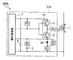
- FIG. 1 is a configuration diagram of a drive circuit according to the first embodiment of the present invention.
- FIG. 2 is a configuration diagram of a drive circuit according to a second embodiment of the present invention.
- FIG. 3 is a configuration diagram of a drive circuit according to a third embodiment of the present invention.
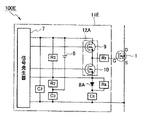
- FIG. 4 is a configuration diagram of a drive circuit according to a fourth embodiment of the present invention.
- FIG. 5 is a configuration diagram of a drive circuit according to a fifth embodiment of the present invention.
- FIG. 6 is a configuration diagram of a driving circuit according to a sixth embodiment of the present invention.
- FIG. 1 is a configuration diagram of a drive circuit according to the first embodiment of the present invention.
- the drive circuit according to the first embodiment uses a MOSFET (Metal Oxide Semiconductor Field Effect Transistor) as an example of the switching element 1 .
- MOSFET Metal Oxide Semiconductor Field Effect Transistor
- a bridge circuit or the like can be configured and used in a power converter or the like.
- the switching element 1 is not limited to unipolar type, bipolar type, and the bandgap of the element material, and can be used.
- the switching element 1 has a gate (control terminal), a drain (high potential terminal), and a source (low potential terminal). It switches between an on state in which current flows and an off state in which no current flows.
- the driving circuit 11 applies a gate voltage to the switching element 1 to switch between an ON state and an OFF state, and operates a push-pull circuit 12, a positive voltage power supply 4, a negative voltage power supply 5, a signal generator 7, It has resistors R2 and R3 and a capacitor C1.
- the push-pull circuit 12 has a PNP transistor 2 (P-type second transistor) and an NPN-type transistor 3 (N-type first transistor) that are connected in series and alternately turn on and off.
- the emitter (first main electrode) of PNP transistor 2 and the emitter (first main electrode) of NPN transistor 3 are connected to the gate of switching element 1 via resistor R1.
- the signal generator 7 applies a drive signal to the base (control electrode) of the PNP transistor 2 and the base (control electrode) of the NPN transistor 3 of the push-pull circuit 12, so that the PNP transistor 2 and the NPN transistor 3 are alternately turned on and off.
- the negative voltage power supply 5 applies a negative voltage to the gate as a voltage when the switching element 1 switches from the ON state to the OFF state.
- the resistor R2 is connected between the negative electrode of the negative voltage power supply 5 and the collector (second main electrode) of the PNP transistor 2, and is a first potential adjusting resistor.
- a capacitor C1 is connected between the positive terminal of the negative voltage power supply 5 and the collector of the PNP transistor 2 .
- the positive electrode of the negative voltage power supply 5 is connected to the capacitor C1 and the source of the switching element 1 .
- a resistor R3 is connected between the collector (second main electrode) and the base of the NPN transistor 3, and is a second potential adjusting resistor.
- the resistor R3 adjusts the gate voltage of the switching element 1 just before it turns on by dividing the voltage of the resistors R2 and R3 when the potentials of the collector and base of the PNP transistor 2 become close when the switching element 1 is turned off.
- the resistor R3 is a resistor that determines the convergence voltage of the gate voltage when the switching element 1 is turned off.
- the gate voltage immediately before the switching element 1 switches from the OFF state to the ON state can be increased.
- a voltage changing unit is configured to change the voltage immediately before switching from the off state to the on state (hereinafter abbreviated as turn-on) to be higher.
- the voltage changer changes the voltage immediately before the switching element 1 turns on to a positive voltage or more and less than the threshold voltage of the switching element 1 . Further, when the switching element 1 is in the OFF state, the voltage changing section holds the negative voltage immediately after the switching element 1 is turned off for a predetermined period. Also, the gate of the switching element 1 has a resistor R1 for adjusting the switching speed.
- a negative voltage (eg, -1 V) is applied as a drive signal from the signal generator 7 to the base of the NPN transistor 3 and the base of the PNP transistor 2 of the push-pull circuit 12 .
- the positive positive voltage e.g. 10V
- the negative negative voltage e.g. -10V
- the NPN transistor 3 is turned off and the PNP transistor 2 is turned on.
- the negative voltage from the negative voltage power supply 5 is applied to the gate of the switching element 1 via the resistor R2, the PNP transistor 2, and the resistor R1. That is, the gate of the switching element 1 becomes a negative voltage, and the switching element 1 is turned off.
- the gate potential of the switching element 1 is initially about -10 V in the previous example, but the gate potential rises as the capacitor C1 is charged. At this time, the switching speed can be increased by reducing the resistance R1. Thereby, the switching loss when the switching element 1 is turned off can be reduced.
- the switching element 1 When the switching element 1 is used in a bridge circuit or the like, immediately after the switching element 1 is turned off, a voltage change occurs between the drain and the source due to the ON operation of the switching element of the other arm. Due to this voltage change, the gate voltage coupled with the parasitic capacitance of the switching element 1 fluctuates.
- the switching element 1 When the fluctuated gate voltage exceeds the threshold voltage of the switching element 1, the switching element 1 is erroneously turned on. At this time, the gate voltage lower than the threshold voltage of the switching element 1 can be maintained by raising the negative voltage of the negative voltage power supply 5, that is, by increasing the negative voltage, or by increasing the capacity of the capacitor C1. As a result, erroneous turn-on of the switching element 1 can be suppressed.
- the gate voltage of the switching element 1 is increased by dividing the voltage of the positive voltage power supply 4, the negative voltage power supply 5, the resistors R2 and R3, and the charge change of the capacitor C1. Rise.
- the gate voltage of the switching element 1 immediately before turning on can be set to a voltage that is less than the threshold voltage of the switching element 1 and close to the threshold voltage in advance. Therefore, in order to turn on the switching element 1, the gate voltage is increased from a voltage less than the threshold voltage of the switching element 1 and close to the threshold voltage to a voltage equal to or higher than the threshold voltage of the switching element 1 by the positive voltage power source 4. Shorten.
- a positive voltage (for example, +1 V) is applied from the signal generator 7 to the base of the NPN transistor 3 and the base of the PNP transistor 2 .
- the positive voltage (e.g., 10 V) of the positive voltage source 4 is applied to the collector of the NPN transistor 3, and the negative electrode (e.g., -10 V) of the negative voltage source 5 is applied to the collector of the PNP transistor 2. .
- the NPN transistor 3 is turned on and the PNP transistor 2 is turned off.
- the positive voltage of the positive voltage power supply 4 is applied to the gate of the switching element 1 via the NPN transistor 3 and the resistor R1. That is, the gate of the switching element 1 becomes equal to or higher than the threshold voltage, and the switching element 1 is turned on.
- the resistors R2 and R3 and the capacitor C1 change the voltage just before the switching element 1 turns on to be higher than the negative voltage from the negative voltage power supply 5 just after the switching element 1 turns off. Therefore, the switching element 1 can be turned on at high speed.
- the resistors R2 and R3 and the capacitor C1 change the voltage just before the switching element 1 turns on to a positive voltage or more and less than the threshold voltage of the switching element 1.
- the switching element 1 can be turned on at high speed by raising the gate voltage of the switching element 1 immediately before turning on to a positive voltage or higher with respect to the source and close to the threshold voltage.
- the voltage changing unit holds the negative voltage immediately after the switching element 1 is turned off for a predetermined period or longer, specifically for a dead time or longer. As a result, it is possible to prevent the switching elements of the upper and lower arms from being turned on at the same time, so that the erroneous turn-on suppressing effect can be enhanced.
- a simple and low-cost circuit configuration including the push-pull circuit 12, the resistors R2 and R3, and the capacitor C1 enables suppression of erroneous turn-on and high-speed turn-on.
- FIG. 2 is a configuration diagram of a drive circuit according to the second embodiment of the present invention.
- the drive circuit according to the second embodiment differs from the drive circuit according to the first embodiment in that a resistor R4 and a diode 8A are provided.
- a resistor R4 and a diode 8A are connected in parallel between the collector of the PNP transistor 2, one end of the resistor R2, and one end of the capacitor C1.
- the anode of diode 8A is connected to the collector of PNP transistor 2, and the cathode of diode 8A is connected to one end of capacitor C1.
- the charge storage time from the negative voltage power supply 5 to the capacitor C1 is adjusted by the value of the resistor R4. can do. If the resistance R4 is small, the charging time will be short, and if the resistance R4 is large, the charging time will be long.
- the gate voltage immediately after turning off the switching element 1 can be changed to any voltage by adjusting the value of the resistor R4, and by making the gate voltage negative with respect to the source, it can be adjusted to the optimum erroneous turn-on suppression voltage. be able to.
- FIG. 3 is a configuration diagram of a drive circuit according to the third embodiment of the present invention.
- the drive circuit according to the third embodiment differs from the drive circuit according to the second embodiment in that the direction of the diode 8B is reversed.
- the cathode of diode 8B is connected to the collector of PNP transistor 2, and the anode of diode 8B is connected to one end of capacitor C1.
- the drive circuit of the third embodiment it is possible to shorten the charge storage time from the negative voltage power supply 5 to the capacitor C1.
- the charge accumulated in the capacitor C1 is discharged to the discharge resistor R4.
- the discharge time can be adjusted by the value of resistor R4.
- the switching speed when the switching element 1 is turned off can be arbitrarily changed, and the amount of change in the gate voltage can be adjusted to the optimum.
- FIG. 4 is a configuration diagram of a drive circuit according to the fourth embodiment of the present invention.
- the drive circuit according to the fourth embodiment differs from the drive circuit according to the second embodiment by using an N-channel MOSFET 9 (N-type transistor) and a P-channel MOSFET 10 (P-type transistor) for the push-pull circuit 12A. It is configured.
- the source of N-channel MOSFET 9 and the source of P-channel MOSFET 10 are connected to the gate of switching element 1 via resistor R1.
- a drive signal is applied to the gate of the N-channel MOSFET 9 and the gate of the P-channel MOSFET 10 .
- the positive terminal of the positive voltage power supply 4 is connected to the drain of the N-channel MOSFET 9 .
- Resistor R3 is connected between the drain of N-channel MOSFET 9 and the source of P-channel MOSFET 10 .
- the same effects as those of the drive circuit according to the second embodiment can be obtained. Further, by using the N-channel MOSFET 9 and the P-channel MOSFET 10, a large current can be passed through the gate of the switching element 1 with a small signal output from the signal generator 7. FIG.
- FIG. 5 is a configuration diagram of a drive circuit according to the fifth embodiment of the present invention.
- the drive circuit according to the fifth embodiment is different from the drive circuit according to the fourth embodiment in that a resistor R5 is provided instead of the positive voltage power supply 4, a resistor R6 is provided instead of the negative voltage power supply 5, and A positive voltage power source 6 is provided.
- the positive electrode of the positive voltage power supply 6 is connected to the drain of the N-channel MOSFET 9, one end of the resistor R3, and one end of the resistor R5.
- the negative electrode of the positive voltage power source 6 is connected to one end of the resistor R2 and one end of the resistor R6.
- the positive voltage of the positive voltage power source 6 is divided by the resistors R5 and R6.
- a current flows from the positive pole of the positive voltage power supply 6 to the negative pole of the positive voltage power supply 6 through the resistors R5 and R6.
- the potential at one end of the resistor R6 is lower than the potential at the source of the switching element 1 and becomes a negative voltage. Therefore, when the P-channel MOSFET 10 is on, the negative voltage at one end of the resistor R6 is applied to the gate of the switching element 1, and the switching element 1 is turned off.
- the positive voltage of the positive voltage power source 6 can be used as the gate voltage of the switching element 1 by dividing it with the resistors R5 and R6.
- a compact drive circuit 11D can be configured using only one positive voltage power supply 6 and passive elements such as the resistors R5 and R6.
- FIG. 6 is a configuration diagram of a drive circuit according to the sixth embodiment of the present invention.
- the drive circuit according to the fourth embodiment is provided with a capacitor C2 instead of the positive voltage power supply 4, a capacitor C3 instead of the negative voltage power supply 5, Furthermore, a positive voltage power supply 6 is provided.
- the positive electrode of the positive voltage power supply 6 is connected to the drain of the N-channel MOSFET 9, one end of the resistor R3, and one end of the capacitor C2.
- the negative electrode of the positive voltage power source 6 is connected to one end of the resistor R2 and one end of the capacitor C3.
- the positive voltage of the positive voltage power source 6 is divided by the capacitors C2 and C3.
- a current flows from the positive pole of the positive voltage power supply 6 to the negative pole of the positive voltage power supply 6 through the capacitors C2 and C3.
- the potential at one end of the capacitor C3 is lower than the potential at the source of the switching element 1 and becomes a negative voltage. Therefore, when the P-channel MOSFET 10 is on, the negative voltage at one end of the capacitor C3 is applied to the gate of the switching element 1, and the switching element 1 is turned off.
- the positive voltage of the positive voltage power supply 6 can be used as the gate voltage of the switching element 1 by dividing it with the capacitors C2 and C3.
- a compact drive circuit 11D can be configured using only the passive elements of the capacitors C2 and C3 using a single positive voltage power supply 6.
- the capacitors C2 and C3 can be charged by transient current flow, the current consumption from the positive voltage power supply 6 can be reduced at all times, resulting in a low-loss drive circuit.
- the drive circuit of the present invention is applicable to switching circuit devices.
Landscapes
- Engineering & Computer Science (AREA)
- Power Engineering (AREA)
- Power Conversion In General (AREA)
- Control Of Indicators Other Than Cathode Ray Tubes (AREA)
Priority Applications (5)
| Application Number | Priority Date | Filing Date | Title |
|---|---|---|---|
| EP21931956.3A EP4318947B1 (en) | 2021-03-22 | 2021-03-22 | Drive circuit |
| US18/283,417 US12126329B2 (en) | 2021-03-22 | 2021-03-22 | Driving circuit |
| JP2023508126A JPWO2022200819A1 (https=) | 2021-03-22 | 2021-03-22 | |
| PCT/IB2021/000184 WO2022200819A1 (ja) | 2021-03-22 | 2021-03-22 | 駆動回路 |
| CN202180095666.8A CN117083803B (zh) | 2021-03-22 | 2021-03-22 | 驱动电路 |
Applications Claiming Priority (1)
| Application Number | Priority Date | Filing Date | Title |
|---|---|---|---|
| PCT/IB2021/000184 WO2022200819A1 (ja) | 2021-03-22 | 2021-03-22 | 駆動回路 |
Publications (2)
| Publication Number | Publication Date |
|---|---|
| WO2022200819A1 true WO2022200819A1 (ja) | 2022-09-29 |
| WO2022200819A8 WO2022200819A8 (ja) | 2023-09-07 |
Family
ID=83395229
Family Applications (1)
| Application Number | Title | Priority Date | Filing Date |
|---|---|---|---|
| PCT/IB2021/000184 Ceased WO2022200819A1 (ja) | 2021-03-22 | 2021-03-22 | 駆動回路 |
Country Status (5)
| Country | Link |
|---|---|
| US (1) | US12126329B2 (https=) |
| EP (1) | EP4318947B1 (https=) |
| JP (1) | JPWO2022200819A1 (https=) |
| CN (1) | CN117083803B (https=) |
| WO (1) | WO2022200819A1 (https=) |
Families Citing this family (1)
| Publication number | Priority date | Publication date | Assignee | Title |
|---|---|---|---|---|
| JP7749979B2 (ja) * | 2021-08-18 | 2025-10-07 | 富士電機株式会社 | 駆動装置 |
Citations (7)
| Publication number | Priority date | Publication date | Assignee | Title |
|---|---|---|---|---|
| JPH11308084A (ja) * | 1998-04-20 | 1999-11-05 | Meidensha Corp | スイッチング素子のゲート駆動回路 |
| JP2001136732A (ja) * | 1999-11-05 | 2001-05-18 | Hitachi Ltd | 半導体電力変換装置 |
| JP2007235859A (ja) * | 2006-03-03 | 2007-09-13 | Kawasaki Heavy Ind Ltd | 自己消弧型半導体素子の駆動装置 |
| JP2011193705A (ja) * | 2010-03-17 | 2011-09-29 | Hitachi Appliances Inc | 電圧駆動型半導体素子のゲート駆動回路及び電力変換装置 |
| JP2014068326A (ja) * | 2012-09-27 | 2014-04-17 | Toyota Central R&D Labs Inc | 駆動回路 |
| WO2017216974A1 (ja) * | 2016-06-17 | 2017-12-21 | 日産自動車株式会社 | 駆動装置 |
| JP2019009846A (ja) | 2017-06-21 | 2019-01-17 | 富士電機株式会社 | ゲート駆動回路およびインバータ装置 |
Family Cites Families (7)
| Publication number | Priority date | Publication date | Assignee | Title |
|---|---|---|---|---|
| US4949213A (en) | 1988-11-16 | 1990-08-14 | Fuji Electric Co., Ltd. | Drive circuit for use with voltage-drive semiconductor device |
| US6201714B1 (en) * | 1999-11-09 | 2001-03-13 | Skynet Electronics Co., Ltd. | Exchanging converter having a zero-voltage switching control circuit for driving an output voltage filter capacitor to partially feed back storage energy to an input side of the transformer or storage inductor |
| JPWO2008155917A1 (ja) | 2007-06-19 | 2010-08-26 | パナソニック株式会社 | スイッチング素子駆動回路 |
| US20100109750A1 (en) * | 2008-10-30 | 2010-05-06 | Jens Barrenscheen | Boost Mechanism Using Driver Current Adjustment for Switching Phase Improvement |
| JP5989265B2 (ja) * | 2014-05-30 | 2016-09-07 | 三菱電機株式会社 | 電力用半導体素子の駆動回路 |
| US9496864B2 (en) * | 2014-12-18 | 2016-11-15 | General Electric Company | Gate drive circuit and method of operating same |
| JP6992498B2 (ja) * | 2017-12-26 | 2022-01-13 | 株式会社デンソー | 駆動対象スイッチの駆動回路 |
-
2021
- 2021-03-22 EP EP21931956.3A patent/EP4318947B1/en active Active
- 2021-03-22 CN CN202180095666.8A patent/CN117083803B/zh active Active
- 2021-03-22 JP JP2023508126A patent/JPWO2022200819A1/ja active Pending
- 2021-03-22 WO PCT/IB2021/000184 patent/WO2022200819A1/ja not_active Ceased
- 2021-03-22 US US18/283,417 patent/US12126329B2/en active Active
Patent Citations (7)
| Publication number | Priority date | Publication date | Assignee | Title |
|---|---|---|---|---|
| JPH11308084A (ja) * | 1998-04-20 | 1999-11-05 | Meidensha Corp | スイッチング素子のゲート駆動回路 |
| JP2001136732A (ja) * | 1999-11-05 | 2001-05-18 | Hitachi Ltd | 半導体電力変換装置 |
| JP2007235859A (ja) * | 2006-03-03 | 2007-09-13 | Kawasaki Heavy Ind Ltd | 自己消弧型半導体素子の駆動装置 |
| JP2011193705A (ja) * | 2010-03-17 | 2011-09-29 | Hitachi Appliances Inc | 電圧駆動型半導体素子のゲート駆動回路及び電力変換装置 |
| JP2014068326A (ja) * | 2012-09-27 | 2014-04-17 | Toyota Central R&D Labs Inc | 駆動回路 |
| WO2017216974A1 (ja) * | 2016-06-17 | 2017-12-21 | 日産自動車株式会社 | 駆動装置 |
| JP2019009846A (ja) | 2017-06-21 | 2019-01-17 | 富士電機株式会社 | ゲート駆動回路およびインバータ装置 |
Non-Patent Citations (1)
| Title |
|---|
| See also references of EP4318947A4 |
Also Published As
| Publication number | Publication date |
|---|---|
| EP4318947A1 (en) | 2024-02-07 |
| WO2022200819A8 (ja) | 2023-09-07 |
| EP4318947B1 (en) | 2025-07-02 |
| CN117083803A (zh) | 2023-11-17 |
| CN117083803B (zh) | 2024-09-27 |
| JPWO2022200819A1 (https=) | 2022-09-29 |
| US20240178829A1 (en) | 2024-05-30 |
| US12126329B2 (en) | 2024-10-22 |
| EP4318947A4 (en) | 2024-05-22 |
Similar Documents
| Publication | Publication Date | Title |
|---|---|---|
| JP5101741B2 (ja) | 半導体装置と、それを用いたインバータ、コンバータおよび電力変換装置 | |
| CN102439831B (zh) | 用于驱动电压驱动型元件的驱动装置 | |
| JP6842837B2 (ja) | ゲート駆動回路 | |
| US20220006450A1 (en) | Driver circuit, corresponding device and method of operation | |
| WO2022070806A1 (ja) | スイッチング素子の駆動回路及びスイッチング回路 | |
| JP2003069401A (ja) | 半導体電力変換装置 | |
| US11831307B2 (en) | Power switch drive circuit and device | |
| JP5407618B2 (ja) | ゲート駆動回路及び電力変換回路 | |
| JP2015012624A (ja) | 駆動回路 | |
| WO2021017538A1 (zh) | 开关电源及其控制电路和控制方法 | |
| JP6956386B2 (ja) | 負電圧生成回路およびこれを用いた電力変換装置 | |
| WO2015033444A1 (ja) | バッファ回路 | |
| CN109861503B (zh) | 用于功率器件的驱动电路 | |
| US6813169B2 (en) | Inverter device capable of reducing through current | |
| JP4779549B2 (ja) | 電圧駆動型半導体素子のゲート駆動回路。 | |
| WO2022200819A1 (ja) | 駆動回路 | |
| CN111869068B (zh) | 开关装置以及开关装置的控制方法 | |
| JP6627351B2 (ja) | スイッチング回路装置 | |
| JP7240835B2 (ja) | スイッチング回路 | |
| US12212224B2 (en) | Driving apparatus | |
| JP7793908B2 (ja) | スイッチング素子の駆動回路及びスイッチング回路 | |
| TW202425513A (zh) | 用於電源轉換設備的控制裝置 | |
| JP2023028099A (ja) | 駆動装置 | |
| WO2020035712A1 (ja) | スイッチング回路 | |
| KR102827085B1 (ko) | 턴온 전압을 승압하여 생성하는 게이트 드라이버 및 이를 구비한 게이트 드라이브 회로 |
Legal Events
| Date | Code | Title | Description |
|---|---|---|---|
| 121 | Ep: the epo has been informed by wipo that ep was designated in this application |
Ref document number: 21931956 Country of ref document: EP Kind code of ref document: A1 |
|
| WWE | Wipo information: entry into national phase |
Ref document number: 2023508126 Country of ref document: JP |
|
| WWE | Wipo information: entry into national phase |
Ref document number: 202180095666.8 Country of ref document: CN |
|
| WWE | Wipo information: entry into national phase |
Ref document number: 18283417 Country of ref document: US |
|
| WWE | Wipo information: entry into national phase |
Ref document number: 2021931956 Country of ref document: EP |
|
| NENP | Non-entry into the national phase |
Ref country code: DE |
|
| ENP | Entry into the national phase |
Ref document number: 2021931956 Country of ref document: EP Effective date: 20231023 |
|
| WWG | Wipo information: grant in national office |
Ref document number: 2021931956 Country of ref document: EP |