EP4318947B1 - Drive circuit - Google Patents
Drive circuit Download PDFInfo
- Publication number
- EP4318947B1 EP4318947B1 EP21931956.3A EP21931956A EP4318947B1 EP 4318947 B1 EP4318947 B1 EP 4318947B1 EP 21931956 A EP21931956 A EP 21931956A EP 4318947 B1 EP4318947 B1 EP 4318947B1
- Authority
- EP
- European Patent Office
- Prior art keywords
- voltage
- switching element
- state
- power supply
- positive
- Prior art date
- Legal status (The legal status is an assumption and is not a legal conclusion. Google has not performed a legal analysis and makes no representation as to the accuracy of the status listed.)
- Active
Links
Images


Classifications
-
- H—ELECTRICITY
- H03—ELECTRONIC CIRCUITRY
- H03K—PULSE TECHNIQUE
- H03K17/00—Electronic switching or gating, i.e. not by contact-making and –breaking
- H03K17/04—Modifications for accelerating switching
- H03K17/041—Modifications for accelerating switching without feedback from the output circuit to the control circuit
- H03K17/0412—Modifications for accelerating switching without feedback from the output circuit to the control circuit by measures taken in the control circuit
- H03K17/04123—Modifications for accelerating switching without feedback from the output circuit to the control circuit by measures taken in the control circuit in field-effect transistor switches
-
- H—ELECTRICITY
- H02—GENERATION; CONVERSION OR DISTRIBUTION OF ELECTRIC POWER
- H02M—APPARATUS FOR CONVERSION BETWEEN AC AND AC, BETWEEN AC AND DC, OR BETWEEN DC AND DC, AND FOR USE WITH MAINS OR SIMILAR POWER SUPPLY SYSTEMS; CONVERSION OF DC OR AC INPUT POWER INTO SURGE OUTPUT POWER; CONTROL OR REGULATION THEREOF
- H02M1/00—Details of apparatus for conversion
- H02M1/0048—Circuits or arrangements for reducing losses
-
- H—ELECTRICITY
- H02—GENERATION; CONVERSION OR DISTRIBUTION OF ELECTRIC POWER
- H02M—APPARATUS FOR CONVERSION BETWEEN AC AND AC, BETWEEN AC AND DC, OR BETWEEN DC AND DC, AND FOR USE WITH MAINS OR SIMILAR POWER SUPPLY SYSTEMS; CONVERSION OF DC OR AC INPUT POWER INTO SURGE OUTPUT POWER; CONTROL OR REGULATION THEREOF
- H02M1/00—Details of apparatus for conversion
- H02M1/08—Circuits specially adapted for the generation of control voltages for semiconductor devices incorporated in static converters
-
- H—ELECTRICITY
- H02—GENERATION; CONVERSION OR DISTRIBUTION OF ELECTRIC POWER
- H02M—APPARATUS FOR CONVERSION BETWEEN AC AND AC, BETWEEN AC AND DC, OR BETWEEN DC AND DC, AND FOR USE WITH MAINS OR SIMILAR POWER SUPPLY SYSTEMS; CONVERSION OF DC OR AC INPUT POWER INTO SURGE OUTPUT POWER; CONTROL OR REGULATION THEREOF
- H02M1/00—Details of apparatus for conversion
- H02M1/38—Means for preventing simultaneous conduction of switches
-
- H—ELECTRICITY
- H03—ELECTRONIC CIRCUITRY
- H03K—PULSE TECHNIQUE
- H03K17/00—Electronic switching or gating, i.e. not by contact-making and –breaking
- H03K17/06—Modifications for ensuring a fully conducting state
- H03K17/063—Modifications for ensuring a fully conducting state in field-effect transistor switches
-
- H—ELECTRICITY
- H03—ELECTRONIC CIRCUITRY
- H03K—PULSE TECHNIQUE
- H03K17/00—Electronic switching or gating, i.e. not by contact-making and –breaking
- H03K17/51—Electronic switching or gating, i.e. not by contact-making and –breaking characterised by the components used
- H03K17/56—Electronic switching or gating, i.e. not by contact-making and –breaking characterised by the components used by the use, as active elements, of semiconductor devices
- H03K17/687—Electronic switching or gating, i.e. not by contact-making and –breaking characterised by the components used by the use, as active elements, of semiconductor devices the devices being field-effect transistors
- H03K17/6871—Electronic switching or gating, i.e. not by contact-making and –breaking characterised by the components used by the use, as active elements, of semiconductor devices the devices being field-effect transistors the output circuit comprising more than one controlled field-effect transistor
-
- H—ELECTRICITY
- H03—ELECTRONIC CIRCUITRY
- H03K—PULSE TECHNIQUE
- H03K17/00—Electronic switching or gating, i.e. not by contact-making and –breaking
- H03K17/06—Modifications for ensuring a fully conducting state
- H03K2017/066—Maximizing the OFF-resistance instead of minimizing the ON-resistance
-
- H—ELECTRICITY
- H03—ELECTRONIC CIRCUITRY
- H03K—PULSE TECHNIQUE
- H03K2217/00—Indexing scheme related to electronic switching or gating, i.e. not by contact-making or -breaking covered by H03K17/00
- H03K2217/0063—High side switches, i.e. the higher potential [DC] or life wire [AC] being directly connected to the switch and not via the load
-
- H—ELECTRICITY
- H03—ELECTRONIC CIRCUITRY
- H03K—PULSE TECHNIQUE
- H03K2217/00—Indexing scheme related to electronic switching or gating, i.e. not by contact-making or -breaking covered by H03K17/00
- H03K2217/0072—Low side switches, i.e. the lower potential [DC] or neutral wire [AC] being directly connected to the switch and not via the load
Definitions
- the present invention relates to a driving circuit.
- a gate driving circuit disclosed in Patent Literature 1 is provided with a gate-off power supply for switching off a switching element connected to a DC power supply and a gate-on power supply for switching on the switching element.
- the gate driving circuit reliably switches the switching element between an ON state and an OFF state by means of the power supply between the gate-off power supply and the gate-on power supply.
- the gate-off power supply for switching off the switching element makes the voltage of the gate-off power supply negative such that the gate potential of the switching element is smaller than the source potential.
- a negative voltage of a gate-off power supply is applied to a gate of a switching element to suppress erroneous turn-on.
- US 2010/109750 A1 discloses a system and method for providing a boost current to a switching transistor gate.
- a boost capacitor precharged to a voltage level above a gate-source voltage is coupled to a switching transistor gate at the beginning of a switch-on phase.
- the boost capacitor is decoupled from the switching transistor gate when a boost capacitor voltage falls below the gate-source voltage and is again precharged to the voltage level above the gate-source voltage.
- a second-phase resistance is coupled between a supply voltage and the switching transistor gate. The second-phase resistance value is selected based upon a current peak detected in the switching transistor.
- a switch-off capacitor precharged to a voltage level below the gate-source voltage may be coupled to the switching transistor gate at the beginning of a switch-of phase.
- US 10 511 302 B2 discloses a drive circuit, in which a control switch is electrically connected between a negative voltage source and a reference voltage generator.
- a drive controller switches a discharge switch and a control switch from an off state to an on state to thereby supply a first negative output voltage to a main control terminal of a target switch.
- the drive controller switches the discharge switch and the control switch from the on state to the off state to thereby change the first negative output voltage to be supplied to the main control terminal of the target switch to a second negative voltage based on the reference voltage generated by the reference voltage generator.
- the second negative voltage is more positive than the first negative voltage.
- US 2010/176783 A1 discloses a switching device drive circuit in which a gate voltage detecting circuit detects a gate voltage of a switching device, and when the gate voltage is less than a predetermined voltage that is set to be less than a threshold voltage of the switching device, outputs an H-level boost instruction signal.
- a voltage control circuit when the boost instruction signal is at the L level, outputs a predetermined voltage of a control power supply as it is, and when the boost instruction signal is at the H level, outputs a voltage obtained by boosting the predetermined voltage.
- the drive signal output circuit amplifies a voltage of a PWM pulse output from a PWM pulse output circuit to a voltage output from the voltage control circuit. Therefore, a drive signal from the drive signal output circuit to the switching device initially becomes the boosted voltage when the PWM pulse goes to the H level, and then becomes the predetermined voltage when the gate voltage of the switching device increases to a predetermined voltage.
- US 4 949 213 A discloses a drive circuit for use with voltage-drive semiconductor device.
- Patent Literature 1 Japanese Patent Unexamined Publication No. 2019-9846
- An object of the present invention is to provide a driving circuit that is capable of suppressing erroneous turn-on and increasing turn-on speed.
- a driving circuit applies a voltage to a switching element to switch between an ON state and an OFF state.
- the switching element includes a control terminal, a high-potential terminal, and a low-potential terminal, and is switched between the ON state in which a current flows between the high-potential terminal and the low-potential terminal and the OFF state in which the current does not flow therebetween, depending on the voltage of the control terminal in a case in which a potential of the low-potential terminal is defined as a reference potential.
- the driving circuit includes a negative-voltage power supply and a voltage changing unit.
- the negative-voltage power supply applies a negative voltage as the voltage to the control terminal when the switching element is switched from the ON state to the OFF state.
- the voltage changing unit changes the voltage immediately before the switching element is switched from the OFF state to the ON state to be higher than the negative voltage from the negative-voltage power supply immediately after the switching element is switched from the ON state to the OFF state.
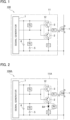
- FIG. 1 is a configuration diagram of a driving circuit according to a first embodiment of the present invention.
- the driving circuit according to the first embodiment uses a MOSFET (Metal Oxide Semiconductor Field Effect Transistor) as an example of a switching element 1.
- MOSFET Metal Oxide Semiconductor Field Effect Transistor
- a plurality of switching elements 1 form a bridge circuit or the like by being arranged in series or parallel, and can be used for a power converter or the like. It should be noted that the switching elements 1 are not limited to unipolar types, bipolar types, bandgaps of element materials, or the like.
- the switching element 1 includes a gate (control terminal), a drain (high-potential terminal) and a source (low-potential terminal), and is switched between an ON state in which a current flows between the drain and the source and an OFF state in which the current does not flow therebetween, depending on a voltage of the gate in a case in which a potential of the source is defined as a reference potential.
- the driving circuit 11 applies a gate voltage to the switching element 1 to switch between an ON state and an OFF state, and includes a push-pull circuit 12, a positive-voltage power supply 4, a negative-voltage power supply 5, a signal generator 7, resistors R2 and R3, and a capacitor C1.
- the push-pull circuit 12 includes a PNP-type transistor 2 (P-type second transistor) and an NPN-type transistor 3 (N-type first transistor) which are connected in series and perform an ON operation and an OFF operation alternately.
- An emitter (first main electrode) of the PNP-type transistor 2 and an emitter (first main electrode) of the NPN-type transistor 3 are connected to the gate of the switching element 1 via a resistor R1.
- the signal generator 7 supplies a drive signal to a base (control electrode) of the PNP-type transistor 2 and a base (control electrode) of the NPN-type transistor 3 in the push-pull circuit 12 to alternately switch the PNP-type transistor 2 and the NPN-type transistor 3 ON and OFF.
- the negative-voltage power supply 5 applies a negative voltage to the gate as a voltage when the switching element 1 is switched from an ON state to an OFF state.
- the resistor R2 is a first potential adjustment resistor that is connected between the negative electrode of the negative-voltage power supply 5 and a collector (second main electrode) of the PNP-type transistor 2.
- the capacitor C1 is connected between the positive electrode of the negative-voltage power supply 5 and the collector of the PNP-type transistor 2.
- the positive electrode of the negative-voltage power supply 5 is connected to the capacitor C1 and the source of the switching element 1.
- the resistor R3 is a second potential adjustment resistor that is connected between a collector (second main electrode) and the base of the NPN-type transistor 3.
- the resistor R3 adjusts the voltage immediately before turn-on of the gate voltage of the switching element 1, by division of voltage by the resistor R2 and the resistor R3. That is, the resistor R3 determines a convergence voltage of the gate voltage when the switching element 1 is OFF.
- the capacitor C1 and the resistors R2 and R3 form a voltage changing unit that changes the voltage immediately before the switching element 1 is switched from the OFF state to the ON state (hereinafter referred to as "turn-on”) to be higher than the negative voltage from the negative-voltage power supply 5 immediately after the switching element 1 is switched from the ON state to the OFF state (hereinafter referred to as "turn-off").
- the voltage changing unit changes the voltage immediately before the switching element 1 is turned off to be greater than the positive voltage and to be less than the threshold voltage of the switching element 1.
- the voltage changing unit also maintains the negative voltage immediately after the switching element 1 is turned off for a predetermined period of time when the switching element 1 is in the OFF state.
- the gate of the switching element 1 also has a resistor R1 that is used to adjust the switching speed.
- a negative voltage (for example, -1 V) is applied as a drive signal from the signal generator 7 to the base of the NPN-type transistor 3 and to the base of the PNP-type transistor 2 of the push-pull circuit 12.
- the positive voltage for example, 10 V
- the negative voltage for example, -10 V
- the NPN-type transistor 3 is switched off and the PNP-type transistor 2 is switched on.
- the negative voltage from the negative-voltage power supply 5 is applied to the gate of the switching element 1 via the resistor R2, the PNP-type transistor 2, and the resistor R1. That is, the gate of the switching element 1 becomes a negative voltage, which causes the switching element 1 to turn off.
- the capacitor C1 is connected in parallel with the gate capacitance of the switching element 1 at the moment when the PNP-type transistor 2 is switched on, thereby rapidly changing the gate potential of the switching element 1.
- the gate potential of the switching element 1 is approximately -10 V in the above example, and the electrical charge is charged to the capacitor C1, thereby increasing the gate potential. At this time, the switching speed can be increased by reducing the resistor R1. This reduces the switching loss when the switching element 1 is turned off.
- the gate voltage that is lower than the threshold voltage of the switching element 1 can be maintained by raising the negative voltage of the negative-voltage power supply 5, that is, by increasing the negative voltage, or by increasing the capacitance of the capacitor C1. This makes it possible to suppress erroneous turn-on of the switching element 1.
- the gate voltage of the switching element 1 increases due to the positive-voltage power supply 4, the negative-voltage power supply 5, the division of voltage by the resistor R2 and the resistor R3, and the change in the electrical charge of the capacitor C1.
- the gate voltage immediately before the switching element 1 is turned on can be set to a voltage that is less than the threshold voltage of the switching element 1 and close to the threshold voltage in advance. Therefore, in order to switch on the switching element 1, the gate voltage is increased from the voltage that is less than the threshold voltage of the switching element 1 and close to the threshold voltage to a voltage that is greater than the threshold voltage of the switching element 1 from the positive-voltage power supply 4, which results in a shorter turn-on time.
- a positive voltage (for example, +1 V) is applied from the signal generator 7 to the base of the NPN-type transistor 3 and the base of the PNP-type transistor 2.
- the positive voltage (for example, 10 V) of the positive electrode of the positive-voltage power supply 4 is applied to the collector of the NPN-type transistor 3, and the negative electrode (for example, -10 V) of the negative-voltage power supply 5 is applied to the collector of the PNP-type transistor 2. This switches on the NPN-type transistor 3 and switches off the PNP-type transistor 2.
- the driving circuit according to the first embodiment makes it possible to suppress erroneous turn-on by reducing the gate voltage immediately after the switching element 1 is turned off to the negative voltage.
- the voltage changing unit maintains the negative voltage immediately after the switching element 1 is turned off for a predetermined period of time or longer, more specifically, for the dead time or longer. This makes it possible to prevent switching elements of upper and lower arms from switching ON simultaneously, thereby enhancing the effect of suppressing erroneous turn-on.
- the gate voltage immediately after the switching element 1 is turned off can be changed to any voltage by adjusting the value of the resistor R4, and the optimal erroneous turn-on suppression voltage can be obtained by changing the gate voltage to the negative voltage with respect to the source.
- the driving circuit according to the fourth embodiment makes it possible to obtain the same effect as that of the driving circuit according to the second embodiment. Further, the use of the N-channel MOSFET 9 and the P-channel MOSFET 10 makes it possible to pass a large current through the gate of the switching element 1 with a smaller signal output from the signal generator 7.
- a positive electrode of the positive-voltage power supply 6 is connected to the drain of the N-channel MOSFET 9, one end of the resistor R3, and one end of the resistor R5.
- a negative electrode of positive-voltage power supply 6 is connected to one end of the resistor R2 and one end of the resistor R6.
- the positive voltage of the positive-voltage power supply 6 is divided by the resistor R5 and the resistor R6.
- a current flows from the positive electrode of the positive-voltage power supply 6 to the negative electrode of the positive-voltage power supply 6 via the resistor R5 and the resistor R6.
- FIG. 6 is a configuration diagram of a driving circuit according to a second comparative example.
- the driving circuit according to this example differs from the driving circuit according to the fourth embodiment of the invention in that a capacitor C2 is provided in place of the positive-voltage power supply 4, a capacitor C3 is provided in place of the negative-voltage power supply 5, and a positive-voltage power supply 6 is further provided.
- the positive voltage of the positive-voltage power supply 6 is divided by the capacitor C2 and the capacitor C3.
- a current transitionally flows from the positive electrode of the positive-voltage power supply 6 to the negative electrode of the positive-voltage power supply 6 via the capacitor C2 and the capacitor C3.
- the source of the switching element 1 is connected to the other end of the capacitor C3, which makes the potential of one end of the capacitor C3 to be lower than the potential of the source of the switching element 1 and results in a negative voltage. For this reason, when the P-channel MOSFET 10 is ON, the negative voltage of one end of the capacitor C3 is applied to the gate of the switching element 1, thereby causing the switching element 1 to turn off.
- the driving circuit of the present invention is applicable to switching circuit devices.
Landscapes
- Engineering & Computer Science (AREA)
- Power Engineering (AREA)
- Power Conversion In General (AREA)
- Control Of Indicators Other Than Cathode Ray Tubes (AREA)
Applications Claiming Priority (1)
| Application Number | Priority Date | Filing Date | Title |
|---|---|---|---|
| PCT/IB2021/000184 WO2022200819A1 (ja) | 2021-03-22 | 2021-03-22 | 駆動回路 |
Publications (3)
| Publication Number | Publication Date |
|---|---|
| EP4318947A1 EP4318947A1 (en) | 2024-02-07 |
| EP4318947A4 EP4318947A4 (en) | 2024-05-22 |
| EP4318947B1 true EP4318947B1 (en) | 2025-07-02 |
Family
ID=83395229
Family Applications (1)
| Application Number | Title | Priority Date | Filing Date |
|---|---|---|---|
| EP21931956.3A Active EP4318947B1 (en) | 2021-03-22 | 2021-03-22 | Drive circuit |
Country Status (5)
| Country | Link |
|---|---|
| US (1) | US12126329B2 (https=) |
| EP (1) | EP4318947B1 (https=) |
| JP (1) | JPWO2022200819A1 (https=) |
| CN (1) | CN117083803B (https=) |
| WO (1) | WO2022200819A1 (https=) |
Families Citing this family (1)
| Publication number | Priority date | Publication date | Assignee | Title |
|---|---|---|---|---|
| JP7749979B2 (ja) * | 2021-08-18 | 2025-10-07 | 富士電機株式会社 | 駆動装置 |
Family Cites Families (14)
| Publication number | Priority date | Publication date | Assignee | Title |
|---|---|---|---|---|
| US4949213A (en) | 1988-11-16 | 1990-08-14 | Fuji Electric Co., Ltd. | Drive circuit for use with voltage-drive semiconductor device |
| JP3769932B2 (ja) | 1998-04-20 | 2006-04-26 | 株式会社明電舎 | スイッチング素子のゲート駆動回路 |
| JP3770008B2 (ja) * | 1999-11-05 | 2006-04-26 | 株式会社日立製作所 | 半導体電力変換装置 |
| US6201714B1 (en) * | 1999-11-09 | 2001-03-13 | Skynet Electronics Co., Ltd. | Exchanging converter having a zero-voltage switching control circuit for driving an output voltage filter capacitor to partially feed back storage energy to an input side of the transformer or storage inductor |
| JP4768476B2 (ja) * | 2006-03-03 | 2011-09-07 | 川崎重工業株式会社 | 自己消弧型半導体素子の駆動装置 |
| JPWO2008155917A1 (ja) | 2007-06-19 | 2010-08-26 | パナソニック株式会社 | スイッチング素子駆動回路 |
| US20100109750A1 (en) * | 2008-10-30 | 2010-05-06 | Jens Barrenscheen | Boost Mechanism Using Driver Current Adjustment for Switching Phase Improvement |
| JP5130310B2 (ja) | 2010-03-17 | 2013-01-30 | 日立アプライアンス株式会社 | 電圧駆動型半導体素子のゲート駆動回路及び電力変換装置 |
| JP5827609B2 (ja) * | 2012-09-27 | 2015-12-02 | 株式会社豊田中央研究所 | 駆動回路 |
| JP5989265B2 (ja) * | 2014-05-30 | 2016-09-07 | 三菱電機株式会社 | 電力用半導体素子の駆動回路 |
| US9496864B2 (en) * | 2014-12-18 | 2016-11-15 | General Electric Company | Gate drive circuit and method of operating same |
| CN109314509B (zh) * | 2016-06-17 | 2020-03-10 | 日产自动车株式会社 | 驱动装置 |
| JP6904091B2 (ja) | 2017-06-21 | 2021-07-14 | 富士電機株式会社 | ゲート駆動回路およびインバータ装置 |
| JP6992498B2 (ja) * | 2017-12-26 | 2022-01-13 | 株式会社デンソー | 駆動対象スイッチの駆動回路 |
-
2021
- 2021-03-22 EP EP21931956.3A patent/EP4318947B1/en active Active
- 2021-03-22 CN CN202180095666.8A patent/CN117083803B/zh active Active
- 2021-03-22 JP JP2023508126A patent/JPWO2022200819A1/ja active Pending
- 2021-03-22 WO PCT/IB2021/000184 patent/WO2022200819A1/ja not_active Ceased
- 2021-03-22 US US18/283,417 patent/US12126329B2/en active Active
Also Published As
| Publication number | Publication date |
|---|---|
| EP4318947A1 (en) | 2024-02-07 |
| WO2022200819A8 (ja) | 2023-09-07 |
| CN117083803A (zh) | 2023-11-17 |
| CN117083803B (zh) | 2024-09-27 |
| WO2022200819A1 (ja) | 2022-09-29 |
| JPWO2022200819A1 (https=) | 2022-09-29 |
| US20240178829A1 (en) | 2024-05-30 |
| US12126329B2 (en) | 2024-10-22 |
| EP4318947A4 (en) | 2024-05-22 |
Similar Documents
| Publication | Publication Date | Title |
|---|---|---|
| EP3754847B1 (en) | Switched capacitor driving circuits for power semiconductors | |
| US11245324B2 (en) | Switching converter and a method thereof | |
| US6285235B1 (en) | Gate control circuit for voltage drive switching element | |
| US11368093B2 (en) | Switching power supply device | |
| JP2005295794A (ja) | アクティブダイオード | |
| US8030986B2 (en) | Power transistor with turn off control and method for operating | |
| EP3787164A1 (en) | Gate drive circuit and gate drive method | |
| CN112640279B (zh) | 过电流保护电路及开关电路 | |
| US7848125B2 (en) | Keep-alive for power stage with multiple switch nodes | |
| CN107769554B (zh) | 开关电源装置的控制电路和开关电源装置 | |
| US7551004B2 (en) | Inverter apparatus with improved gate drive for power MOSFET | |
| EP4318947B1 (en) | Drive circuit | |
| JP2023134570A (ja) | 出力トランジスタの駆動回路、半導体装置、自動車 | |
| JP7099199B2 (ja) | 駆動対象スイッチの駆動回路 | |
| US20260018997A1 (en) | Power supply control device | |
| US20040145918A1 (en) | Inverter device capable of reducing through-type current | |
| WO2023062745A1 (ja) | 電力用半導体素子の駆動回路、電力用半導体モジュール、および電力変換装置 | |
| CN219576854U (zh) | D型氮化镓开关驱动电路以及开关电源电路 | |
| US10075076B1 (en) | Voltage converter with current steering | |
| JP4319336B2 (ja) | Mosスイッチング回路 | |
| US20190363705A1 (en) | Switch circuit and power source apparatus | |
| CN116094292A (zh) | D型氮化镓开关驱动电路以及开关电源电路 | |
| EP4546648A1 (en) | Driver circuit for a power transistor | |
| CN117767711B (zh) | 单向导通电路、桥式驱动电路及开关电源 | |
| US20250015706A1 (en) | Gate driving device and power converter |
Legal Events
| Date | Code | Title | Description |
|---|---|---|---|
| STAA | Information on the status of an ep patent application or granted ep patent |
Free format text: STATUS: THE INTERNATIONAL PUBLICATION HAS BEEN MADE |
|
| PUAI | Public reference made under article 153(3) epc to a published international application that has entered the european phase |
Free format text: ORIGINAL CODE: 0009012 |
|
| STAA | Information on the status of an ep patent application or granted ep patent |
Free format text: STATUS: REQUEST FOR EXAMINATION WAS MADE |
|
| 17P | Request for examination filed |
Effective date: 20230907 |
|
| AK | Designated contracting states |
Kind code of ref document: A1 Designated state(s): AL AT BE BG CH CY CZ DE DK EE ES FI FR GB GR HR HU IE IS IT LI LT LU LV MC MK MT NL NO PL PT RO RS SE SI SK SM TR |
|
| A4 | Supplementary search report drawn up and despatched |
Effective date: 20240423 |
|
| RIC1 | Information provided on ipc code assigned before grant |
Ipc: H02M 1/38 20070101ALI20240417BHEP Ipc: H02M 1/08 20060101ALI20240417BHEP Ipc: H03K 17/687 20060101ALI20240417BHEP Ipc: H03K 17/60 20060101ALI20240417BHEP Ipc: H03K 17/04 20060101AFI20240417BHEP |
|
| DAV | Request for validation of the european patent (deleted) | ||
| DAX | Request for extension of the european patent (deleted) | ||
| STAA | Information on the status of an ep patent application or granted ep patent |
Free format text: STATUS: EXAMINATION IS IN PROGRESS |
|
| 17Q | First examination report despatched |
Effective date: 20241004 |
|
| REG | Reference to a national code |
Free format text: PREVIOUS MAIN CLASS: H03K0017040000 Ref country code: DE Ref legal event code: R079 Ref document number: 602021033604 Country of ref document: DE Free format text: PREVIOUS MAIN CLASS: H03K0017040000 Ipc: H03K0017041200 |
|
| RIC1 | Information provided on ipc code assigned before grant |
Ipc: H02M 1/38 20070101ALI20250327BHEP Ipc: H02M 1/08 20060101ALI20250327BHEP Ipc: H03K 17/06 20060101ALI20250327BHEP Ipc: H03K 17/0412 20060101AFI20250327BHEP |
|
| GRAP | Despatch of communication of intention to grant a patent |
Free format text: ORIGINAL CODE: EPIDOSNIGR1 |
|
| STAA | Information on the status of an ep patent application or granted ep patent |
Free format text: STATUS: GRANT OF PATENT IS INTENDED |
|
| GRAS | Grant fee paid |
Free format text: ORIGINAL CODE: EPIDOSNIGR3 |
|
| GRAA | (expected) grant |
Free format text: ORIGINAL CODE: 0009210 |
|
| STAA | Information on the status of an ep patent application or granted ep patent |
Free format text: STATUS: THE PATENT HAS BEEN GRANTED |
|
| INTG | Intention to grant announced |
Effective date: 20250508 |
|
| AK | Designated contracting states |
Kind code of ref document: B1 Designated state(s): AL AT BE BG CH CY CZ DE DK EE ES FI FR GB GR HR HU IE IS IT LI LT LU LV MC MK MT NL NO PL PT RO RS SE SI SK SM TR |
|
| REG | Reference to a national code |
Ref country code: GB Ref legal event code: FG4D |
|
| REG | Reference to a national code |
Ref country code: CH Ref legal event code: EP |
|
| REG | Reference to a national code |
Ref country code: DE Ref legal event code: R096 Ref document number: 602021033604 Country of ref document: DE |
|
| REG | Reference to a national code |
Ref country code: IE Ref legal event code: FG4D |
|
| REG | Reference to a national code |
Ref country code: NL Ref legal event code: MP Effective date: 20250702 |
|
| PG25 | Lapsed in a contracting state [announced via postgrant information from national office to epo] |
Ref country code: PT Free format text: LAPSE BECAUSE OF FAILURE TO SUBMIT A TRANSLATION OF THE DESCRIPTION OR TO PAY THE FEE WITHIN THE PRESCRIBED TIME-LIMIT Effective date: 20251103 |
|
| PG25 | Lapsed in a contracting state [announced via postgrant information from national office to epo] |
Ref country code: NL Free format text: LAPSE BECAUSE OF FAILURE TO SUBMIT A TRANSLATION OF THE DESCRIPTION OR TO PAY THE FEE WITHIN THE PRESCRIBED TIME-LIMIT Effective date: 20250702 |
|
| REG | Reference to a national code |
Ref country code: AT Ref legal event code: MK05 Ref document number: 1810446 Country of ref document: AT Kind code of ref document: T Effective date: 20250702 |
|
| PG25 | Lapsed in a contracting state [announced via postgrant information from national office to epo] |
Ref country code: IS Free format text: LAPSE BECAUSE OF FAILURE TO SUBMIT A TRANSLATION OF THE DESCRIPTION OR TO PAY THE FEE WITHIN THE PRESCRIBED TIME-LIMIT Effective date: 20251102 |
|
| PG25 | Lapsed in a contracting state [announced via postgrant information from national office to epo] |
Ref country code: NO Free format text: LAPSE BECAUSE OF FAILURE TO SUBMIT A TRANSLATION OF THE DESCRIPTION OR TO PAY THE FEE WITHIN THE PRESCRIBED TIME-LIMIT Effective date: 20251002 |
|
| REG | Reference to a national code |
Ref country code: LT Ref legal event code: MG9D |
|
| PG25 | Lapsed in a contracting state [announced via postgrant information from national office to epo] |
Ref country code: AT Free format text: LAPSE BECAUSE OF FAILURE TO SUBMIT A TRANSLATION OF THE DESCRIPTION OR TO PAY THE FEE WITHIN THE PRESCRIBED TIME-LIMIT Effective date: 20250702 |
|
| PG25 | Lapsed in a contracting state [announced via postgrant information from national office to epo] |
Ref country code: FI Free format text: LAPSE BECAUSE OF FAILURE TO SUBMIT A TRANSLATION OF THE DESCRIPTION OR TO PAY THE FEE WITHIN THE PRESCRIBED TIME-LIMIT Effective date: 20250702 |
|
| PG25 | Lapsed in a contracting state [announced via postgrant information from national office to epo] |
Ref country code: HR Free format text: LAPSE BECAUSE OF FAILURE TO SUBMIT A TRANSLATION OF THE DESCRIPTION OR TO PAY THE FEE WITHIN THE PRESCRIBED TIME-LIMIT Effective date: 20250702 |
|
| PG25 | Lapsed in a contracting state [announced via postgrant information from national office to epo] |
Ref country code: GR Free format text: LAPSE BECAUSE OF FAILURE TO SUBMIT A TRANSLATION OF THE DESCRIPTION OR TO PAY THE FEE WITHIN THE PRESCRIBED TIME-LIMIT Effective date: 20251003 |
|
| PG25 | Lapsed in a contracting state [announced via postgrant information from national office to epo] |
Ref country code: CZ Free format text: LAPSE BECAUSE OF FAILURE TO SUBMIT A TRANSLATION OF THE DESCRIPTION OR TO PAY THE FEE WITHIN THE PRESCRIBED TIME-LIMIT Effective date: 20250702 Ref country code: SE Free format text: LAPSE BECAUSE OF FAILURE TO SUBMIT A TRANSLATION OF THE DESCRIPTION OR TO PAY THE FEE WITHIN THE PRESCRIBED TIME-LIMIT Effective date: 20250702 |
|
| PG25 | Lapsed in a contracting state [announced via postgrant information from national office to epo] |
Ref country code: LV Free format text: LAPSE BECAUSE OF FAILURE TO SUBMIT A TRANSLATION OF THE DESCRIPTION OR TO PAY THE FEE WITHIN THE PRESCRIBED TIME-LIMIT Effective date: 20250702 |
|
| PG25 | Lapsed in a contracting state [announced via postgrant information from national office to epo] |
Ref country code: BG Free format text: LAPSE BECAUSE OF FAILURE TO SUBMIT A TRANSLATION OF THE DESCRIPTION OR TO PAY THE FEE WITHIN THE PRESCRIBED TIME-LIMIT Effective date: 20250702 Ref country code: PL Free format text: LAPSE BECAUSE OF FAILURE TO SUBMIT A TRANSLATION OF THE DESCRIPTION OR TO PAY THE FEE WITHIN THE PRESCRIBED TIME-LIMIT Effective date: 20250702 |
|
| PG25 | Lapsed in a contracting state [announced via postgrant information from national office to epo] |
Ref country code: RS Free format text: LAPSE BECAUSE OF FAILURE TO SUBMIT A TRANSLATION OF THE DESCRIPTION OR TO PAY THE FEE WITHIN THE PRESCRIBED TIME-LIMIT Effective date: 20251002 |
|
| PG25 | Lapsed in a contracting state [announced via postgrant information from national office to epo] |
Ref country code: ES Free format text: LAPSE BECAUSE OF FAILURE TO SUBMIT A TRANSLATION OF THE DESCRIPTION OR TO PAY THE FEE WITHIN THE PRESCRIBED TIME-LIMIT Effective date: 20250702 |
|
| PG25 | Lapsed in a contracting state [announced via postgrant information from national office to epo] |
Ref country code: SM Free format text: LAPSE BECAUSE OF FAILURE TO SUBMIT A TRANSLATION OF THE DESCRIPTION OR TO PAY THE FEE WITHIN THE PRESCRIBED TIME-LIMIT Effective date: 20250702 |
|
| PGFP | Annual fee paid to national office [announced via postgrant information from national office to epo] |
Ref country code: GB Payment date: 20260324 Year of fee payment: 6 |
|
| PG25 | Lapsed in a contracting state [announced via postgrant information from national office to epo] |
Ref country code: DK Free format text: LAPSE BECAUSE OF FAILURE TO SUBMIT A TRANSLATION OF THE DESCRIPTION OR TO PAY THE FEE WITHIN THE PRESCRIBED TIME-LIMIT Effective date: 20250702 |
|
| PGFP | Annual fee paid to national office [announced via postgrant information from national office to epo] |
Ref country code: DE Payment date: 20260327 Year of fee payment: 6 |
|
| PG25 | Lapsed in a contracting state [announced via postgrant information from national office to epo] |
Ref country code: IT Free format text: LAPSE BECAUSE OF FAILURE TO SUBMIT A TRANSLATION OF THE DESCRIPTION OR TO PAY THE FEE WITHIN THE PRESCRIBED TIME-LIMIT Effective date: 20250702 |
|
| PGFP | Annual fee paid to national office [announced via postgrant information from national office to epo] |
Ref country code: FR Payment date: 20260324 Year of fee payment: 6 |
|
| PG25 | Lapsed in a contracting state [announced via postgrant information from national office to epo] |
Ref country code: SK Free format text: LAPSE BECAUSE OF FAILURE TO SUBMIT A TRANSLATION OF THE DESCRIPTION OR TO PAY THE FEE WITHIN THE PRESCRIBED TIME-LIMIT Effective date: 20250702 Ref country code: EE Free format text: LAPSE BECAUSE OF FAILURE TO SUBMIT A TRANSLATION OF THE DESCRIPTION OR TO PAY THE FEE WITHIN THE PRESCRIBED TIME-LIMIT Effective date: 20250702 |