WO2022200819A1 - Drive circuit - Google Patents
Drive circuit Download PDFInfo
- Publication number
- WO2022200819A1 WO2022200819A1 PCT/IB2021/000184 IB2021000184W WO2022200819A1 WO 2022200819 A1 WO2022200819 A1 WO 2022200819A1 IB 2021000184 W IB2021000184 W IB 2021000184W WO 2022200819 A1 WO2022200819 A1 WO 2022200819A1
- Authority
- WO
- WIPO (PCT)
- Prior art keywords
- voltage
- state
- switching element
- transistor
- terminal
- Prior art date
Links
- 239000003990 capacitor Substances 0.000 claims description 38
- 238000010586 diagram Methods 0.000 description 12
- 230000000694 effects Effects 0.000 description 2
- 230000001629 suppression Effects 0.000 description 2
- 238000006243 chemical reaction Methods 0.000 description 1
- 230000005669 field effect Effects 0.000 description 1
- 239000000463 material Substances 0.000 description 1
- 229910044991 metal oxide Inorganic materials 0.000 description 1
- 150000004706 metal oxides Chemical class 0.000 description 1
- 230000003071 parasitic effect Effects 0.000 description 1
- 239000004065 semiconductor Substances 0.000 description 1
- 230000001052 transient effect Effects 0.000 description 1
Images


Classifications
-
- H—ELECTRICITY
- H03—ELECTRONIC CIRCUITRY
- H03K—PULSE TECHNIQUE
- H03K17/00—Electronic switching or gating, i.e. not by contact-making and –breaking
- H03K17/04—Modifications for accelerating switching
- H03K17/041—Modifications for accelerating switching without feedback from the output circuit to the control circuit
- H03K17/0412—Modifications for accelerating switching without feedback from the output circuit to the control circuit by measures taken in the control circuit
- H03K17/04123—Modifications for accelerating switching without feedback from the output circuit to the control circuit by measures taken in the control circuit in field-effect transistor switches
-
- H—ELECTRICITY
- H02—GENERATION; CONVERSION OR DISTRIBUTION OF ELECTRIC POWER
- H02M—APPARATUS FOR CONVERSION BETWEEN AC AND AC, BETWEEN AC AND DC, OR BETWEEN DC AND DC, AND FOR USE WITH MAINS OR SIMILAR POWER SUPPLY SYSTEMS; CONVERSION OF DC OR AC INPUT POWER INTO SURGE OUTPUT POWER; CONTROL OR REGULATION THEREOF
- H02M1/00—Details of apparatus for conversion
- H02M1/0048—Circuits or arrangements for reducing losses
-
- H—ELECTRICITY
- H02—GENERATION; CONVERSION OR DISTRIBUTION OF ELECTRIC POWER
- H02M—APPARATUS FOR CONVERSION BETWEEN AC AND AC, BETWEEN AC AND DC, OR BETWEEN DC AND DC, AND FOR USE WITH MAINS OR SIMILAR POWER SUPPLY SYSTEMS; CONVERSION OF DC OR AC INPUT POWER INTO SURGE OUTPUT POWER; CONTROL OR REGULATION THEREOF
- H02M1/00—Details of apparatus for conversion
- H02M1/08—Circuits specially adapted for the generation of control voltages for semiconductor devices incorporated in static converters
-
- H—ELECTRICITY
- H02—GENERATION; CONVERSION OR DISTRIBUTION OF ELECTRIC POWER
- H02M—APPARATUS FOR CONVERSION BETWEEN AC AND AC, BETWEEN AC AND DC, OR BETWEEN DC AND DC, AND FOR USE WITH MAINS OR SIMILAR POWER SUPPLY SYSTEMS; CONVERSION OF DC OR AC INPUT POWER INTO SURGE OUTPUT POWER; CONTROL OR REGULATION THEREOF
- H02M1/00—Details of apparatus for conversion
- H02M1/38—Means for preventing simultaneous conduction of switches
-
- H—ELECTRICITY
- H03—ELECTRONIC CIRCUITRY
- H03K—PULSE TECHNIQUE
- H03K17/00—Electronic switching or gating, i.e. not by contact-making and –breaking
- H03K17/06—Modifications for ensuring a fully conducting state
- H03K17/063—Modifications for ensuring a fully conducting state in field-effect transistor switches
-
- H—ELECTRICITY
- H03—ELECTRONIC CIRCUITRY
- H03K—PULSE TECHNIQUE
- H03K17/00—Electronic switching or gating, i.e. not by contact-making and –breaking
- H03K17/06—Modifications for ensuring a fully conducting state
- H03K2017/066—Maximizing the OFF-resistance instead of minimizing the ON-resistance
Definitions
- the present invention relates to drive circuits.
- the gate drive circuit described in Patent Document 1 includes a gate-off power supply for turning off switching elements connected to a DC power supply and a gate-on power supply for turning on the switching elements.
- the gate drive circuit reliably switches ON/OFF of the switching element by supplying power from a gate-off power supply and a gate-on power supply.
- the gate-off power supply for turning off the switching element sets the voltage of the gate-off power supply to a negative voltage so that the gate potential of the switching element is smaller than the source potential.
- An object of the present invention is to provide a drive circuit that suppresses erroneous turn-on and speeds up turn-on.
- a drive circuit applies a voltage to a switching element to switch between an ON state and an OFF state.
- the switching element has a control terminal, a high potential terminal, and a low potential terminal, and current flows between the high potential terminal and the low potential terminal according to the voltage of the control terminal when the potential of the low potential terminal is used as a reference potential. is switched between an on state in which current flows and an off state in which no current flows.
- the drive circuit includes a negative voltage power source and a voltage changer.
- the negative voltage power source applies a negative voltage to the control terminal as a voltage when the switching element switches from the ON state to the OFF state.
- the voltage changer changes the voltage immediately before the switching element switches from the off state to the on state higher than the negative voltage from the negative voltage power source immediately after the switching element switches from the on state to the off state.
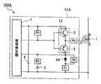
- FIG. 1 is a configuration diagram of a drive circuit according to the first embodiment of the present invention.
- FIG. 2 is a configuration diagram of a drive circuit according to a second embodiment of the present invention.
- FIG. 3 is a configuration diagram of a drive circuit according to a third embodiment of the present invention.
- FIG. 4 is a configuration diagram of a drive circuit according to a fourth embodiment of the present invention.
- FIG. 5 is a configuration diagram of a drive circuit according to a fifth embodiment of the present invention.
- FIG. 6 is a configuration diagram of a driving circuit according to a sixth embodiment of the present invention.
- FIG. 1 is a configuration diagram of a drive circuit according to the first embodiment of the present invention.
- the drive circuit according to the first embodiment uses a MOSFET (Metal Oxide Semiconductor Field Effect Transistor) as an example of the switching element 1 .
- MOSFET Metal Oxide Semiconductor Field Effect Transistor
- a bridge circuit or the like can be configured and used in a power converter or the like.
- the switching element 1 is not limited to unipolar type, bipolar type, and the bandgap of the element material, and can be used.
- the switching element 1 has a gate (control terminal), a drain (high potential terminal), and a source (low potential terminal). It switches between an on state in which current flows and an off state in which no current flows.
- the driving circuit 11 applies a gate voltage to the switching element 1 to switch between an ON state and an OFF state, and operates a push-pull circuit 12, a positive voltage power supply 4, a negative voltage power supply 5, a signal generator 7, It has resistors R2 and R3 and a capacitor C1.
- the push-pull circuit 12 has a PNP transistor 2 (P-type second transistor) and an NPN-type transistor 3 (N-type first transistor) that are connected in series and alternately turn on and off.
- the emitter (first main electrode) of PNP transistor 2 and the emitter (first main electrode) of NPN transistor 3 are connected to the gate of switching element 1 via resistor R1.
- the signal generator 7 applies a drive signal to the base (control electrode) of the PNP transistor 2 and the base (control electrode) of the NPN transistor 3 of the push-pull circuit 12, so that the PNP transistor 2 and the NPN transistor 3 are alternately turned on and off.
- the negative voltage power supply 5 applies a negative voltage to the gate as a voltage when the switching element 1 switches from the ON state to the OFF state.
- the resistor R2 is connected between the negative electrode of the negative voltage power supply 5 and the collector (second main electrode) of the PNP transistor 2, and is a first potential adjusting resistor.
- a capacitor C1 is connected between the positive terminal of the negative voltage power supply 5 and the collector of the PNP transistor 2 .
- the positive electrode of the negative voltage power supply 5 is connected to the capacitor C1 and the source of the switching element 1 .
- a resistor R3 is connected between the collector (second main electrode) and the base of the NPN transistor 3, and is a second potential adjusting resistor.
- the resistor R3 adjusts the gate voltage of the switching element 1 just before it turns on by dividing the voltage of the resistors R2 and R3 when the potentials of the collector and base of the PNP transistor 2 become close when the switching element 1 is turned off.
- the resistor R3 is a resistor that determines the convergence voltage of the gate voltage when the switching element 1 is turned off.
- the gate voltage immediately before the switching element 1 switches from the OFF state to the ON state can be increased.
- a voltage changing unit is configured to change the voltage immediately before switching from the off state to the on state (hereinafter abbreviated as turn-on) to be higher.
- the voltage changer changes the voltage immediately before the switching element 1 turns on to a positive voltage or more and less than the threshold voltage of the switching element 1 . Further, when the switching element 1 is in the OFF state, the voltage changing section holds the negative voltage immediately after the switching element 1 is turned off for a predetermined period. Also, the gate of the switching element 1 has a resistor R1 for adjusting the switching speed.
- a negative voltage (eg, -1 V) is applied as a drive signal from the signal generator 7 to the base of the NPN transistor 3 and the base of the PNP transistor 2 of the push-pull circuit 12 .
- the positive positive voltage e.g. 10V
- the negative negative voltage e.g. -10V
- the NPN transistor 3 is turned off and the PNP transistor 2 is turned on.
- the negative voltage from the negative voltage power supply 5 is applied to the gate of the switching element 1 via the resistor R2, the PNP transistor 2, and the resistor R1. That is, the gate of the switching element 1 becomes a negative voltage, and the switching element 1 is turned off.
- the gate potential of the switching element 1 is initially about -10 V in the previous example, but the gate potential rises as the capacitor C1 is charged. At this time, the switching speed can be increased by reducing the resistance R1. Thereby, the switching loss when the switching element 1 is turned off can be reduced.
- the switching element 1 When the switching element 1 is used in a bridge circuit or the like, immediately after the switching element 1 is turned off, a voltage change occurs between the drain and the source due to the ON operation of the switching element of the other arm. Due to this voltage change, the gate voltage coupled with the parasitic capacitance of the switching element 1 fluctuates.
- the switching element 1 When the fluctuated gate voltage exceeds the threshold voltage of the switching element 1, the switching element 1 is erroneously turned on. At this time, the gate voltage lower than the threshold voltage of the switching element 1 can be maintained by raising the negative voltage of the negative voltage power supply 5, that is, by increasing the negative voltage, or by increasing the capacity of the capacitor C1. As a result, erroneous turn-on of the switching element 1 can be suppressed.
- the gate voltage of the switching element 1 is increased by dividing the voltage of the positive voltage power supply 4, the negative voltage power supply 5, the resistors R2 and R3, and the charge change of the capacitor C1. Rise.
- the gate voltage of the switching element 1 immediately before turning on can be set to a voltage that is less than the threshold voltage of the switching element 1 and close to the threshold voltage in advance. Therefore, in order to turn on the switching element 1, the gate voltage is increased from a voltage less than the threshold voltage of the switching element 1 and close to the threshold voltage to a voltage equal to or higher than the threshold voltage of the switching element 1 by the positive voltage power source 4. Shorten.
- a positive voltage (for example, +1 V) is applied from the signal generator 7 to the base of the NPN transistor 3 and the base of the PNP transistor 2 .
- the positive voltage (e.g., 10 V) of the positive voltage source 4 is applied to the collector of the NPN transistor 3, and the negative electrode (e.g., -10 V) of the negative voltage source 5 is applied to the collector of the PNP transistor 2. .
- the NPN transistor 3 is turned on and the PNP transistor 2 is turned off.
- the positive voltage of the positive voltage power supply 4 is applied to the gate of the switching element 1 via the NPN transistor 3 and the resistor R1. That is, the gate of the switching element 1 becomes equal to or higher than the threshold voltage, and the switching element 1 is turned on.
- the resistors R2 and R3 and the capacitor C1 change the voltage just before the switching element 1 turns on to be higher than the negative voltage from the negative voltage power supply 5 just after the switching element 1 turns off. Therefore, the switching element 1 can be turned on at high speed.
- the resistors R2 and R3 and the capacitor C1 change the voltage just before the switching element 1 turns on to a positive voltage or more and less than the threshold voltage of the switching element 1.
- the switching element 1 can be turned on at high speed by raising the gate voltage of the switching element 1 immediately before turning on to a positive voltage or higher with respect to the source and close to the threshold voltage.
- the voltage changing unit holds the negative voltage immediately after the switching element 1 is turned off for a predetermined period or longer, specifically for a dead time or longer. As a result, it is possible to prevent the switching elements of the upper and lower arms from being turned on at the same time, so that the erroneous turn-on suppressing effect can be enhanced.
- a simple and low-cost circuit configuration including the push-pull circuit 12, the resistors R2 and R3, and the capacitor C1 enables suppression of erroneous turn-on and high-speed turn-on.
- FIG. 2 is a configuration diagram of a drive circuit according to the second embodiment of the present invention.
- the drive circuit according to the second embodiment differs from the drive circuit according to the first embodiment in that a resistor R4 and a diode 8A are provided.
- a resistor R4 and a diode 8A are connected in parallel between the collector of the PNP transistor 2, one end of the resistor R2, and one end of the capacitor C1.
- the anode of diode 8A is connected to the collector of PNP transistor 2, and the cathode of diode 8A is connected to one end of capacitor C1.
- the charge storage time from the negative voltage power supply 5 to the capacitor C1 is adjusted by the value of the resistor R4. can do. If the resistance R4 is small, the charging time will be short, and if the resistance R4 is large, the charging time will be long.
- the gate voltage immediately after turning off the switching element 1 can be changed to any voltage by adjusting the value of the resistor R4, and by making the gate voltage negative with respect to the source, it can be adjusted to the optimum erroneous turn-on suppression voltage. be able to.
- FIG. 3 is a configuration diagram of a drive circuit according to the third embodiment of the present invention.
- the drive circuit according to the third embodiment differs from the drive circuit according to the second embodiment in that the direction of the diode 8B is reversed.
- the cathode of diode 8B is connected to the collector of PNP transistor 2, and the anode of diode 8B is connected to one end of capacitor C1.
- the drive circuit of the third embodiment it is possible to shorten the charge storage time from the negative voltage power supply 5 to the capacitor C1.
- the charge accumulated in the capacitor C1 is discharged to the discharge resistor R4.
- the discharge time can be adjusted by the value of resistor R4.
- the switching speed when the switching element 1 is turned off can be arbitrarily changed, and the amount of change in the gate voltage can be adjusted to the optimum.
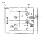
- FIG. 4 is a configuration diagram of a drive circuit according to the fourth embodiment of the present invention.
- the drive circuit according to the fourth embodiment differs from the drive circuit according to the second embodiment by using an N-channel MOSFET 9 (N-type transistor) and a P-channel MOSFET 10 (P-type transistor) for the push-pull circuit 12A. It is configured.
- the source of N-channel MOSFET 9 and the source of P-channel MOSFET 10 are connected to the gate of switching element 1 via resistor R1.
- a drive signal is applied to the gate of the N-channel MOSFET 9 and the gate of the P-channel MOSFET 10 .
- the positive terminal of the positive voltage power supply 4 is connected to the drain of the N-channel MOSFET 9 .
- Resistor R3 is connected between the drain of N-channel MOSFET 9 and the source of P-channel MOSFET 10 .
- the same effects as those of the drive circuit according to the second embodiment can be obtained. Further, by using the N-channel MOSFET 9 and the P-channel MOSFET 10, a large current can be passed through the gate of the switching element 1 with a small signal output from the signal generator 7. FIG.
- FIG. 5 is a configuration diagram of a drive circuit according to the fifth embodiment of the present invention.
- the drive circuit according to the fifth embodiment is different from the drive circuit according to the fourth embodiment in that a resistor R5 is provided instead of the positive voltage power supply 4, a resistor R6 is provided instead of the negative voltage power supply 5, and A positive voltage power source 6 is provided.
- the positive electrode of the positive voltage power supply 6 is connected to the drain of the N-channel MOSFET 9, one end of the resistor R3, and one end of the resistor R5.
- the negative electrode of the positive voltage power source 6 is connected to one end of the resistor R2 and one end of the resistor R6.
- the positive voltage of the positive voltage power source 6 is divided by the resistors R5 and R6.
- a current flows from the positive pole of the positive voltage power supply 6 to the negative pole of the positive voltage power supply 6 through the resistors R5 and R6.
- the potential at one end of the resistor R6 is lower than the potential at the source of the switching element 1 and becomes a negative voltage. Therefore, when the P-channel MOSFET 10 is on, the negative voltage at one end of the resistor R6 is applied to the gate of the switching element 1, and the switching element 1 is turned off.
- the positive voltage of the positive voltage power source 6 can be used as the gate voltage of the switching element 1 by dividing it with the resistors R5 and R6.
- a compact drive circuit 11D can be configured using only one positive voltage power supply 6 and passive elements such as the resistors R5 and R6.
- FIG. 6 is a configuration diagram of a drive circuit according to the sixth embodiment of the present invention.
- the drive circuit according to the fourth embodiment is provided with a capacitor C2 instead of the positive voltage power supply 4, a capacitor C3 instead of the negative voltage power supply 5, Furthermore, a positive voltage power supply 6 is provided.
- the positive electrode of the positive voltage power supply 6 is connected to the drain of the N-channel MOSFET 9, one end of the resistor R3, and one end of the capacitor C2.
- the negative electrode of the positive voltage power source 6 is connected to one end of the resistor R2 and one end of the capacitor C3.
- the positive voltage of the positive voltage power source 6 is divided by the capacitors C2 and C3.
- a current flows from the positive pole of the positive voltage power supply 6 to the negative pole of the positive voltage power supply 6 through the capacitors C2 and C3.
- the potential at one end of the capacitor C3 is lower than the potential at the source of the switching element 1 and becomes a negative voltage. Therefore, when the P-channel MOSFET 10 is on, the negative voltage at one end of the capacitor C3 is applied to the gate of the switching element 1, and the switching element 1 is turned off.
- the positive voltage of the positive voltage power supply 6 can be used as the gate voltage of the switching element 1 by dividing it with the capacitors C2 and C3.
- a compact drive circuit 11D can be configured using only the passive elements of the capacitors C2 and C3 using a single positive voltage power supply 6.
- the capacitors C2 and C3 can be charged by transient current flow, the current consumption from the positive voltage power supply 6 can be reduced at all times, resulting in a low-loss drive circuit.
- the drive circuit of the present invention is applicable to switching circuit devices.
Abstract
Description
(第1の実施形態) Hereinafter, drive circuits according to some embodiments of the present invention will be described in detail with reference to the drawings. The same or corresponding parts in the drawings of the drive circuit according to each embodiment are denoted by the same reference numerals, and descriptions thereof are omitted.
(First embodiment)
(第5の実施形態) As a result, the switching speed of turn-on and turn-off of the
(Fifth embodiment)
(第6の実施形態) That is, the positive voltage of the positive
(Sixth embodiment)
2 PNP型トランジスタ
3 NPN型トランジスタ
4,6 正電圧用電源
5 負電圧用電源
7 信号発生器
8A,8B ダイオード
9 NチャネルMOSFET
10 PチャネルMOSFET
11,11A,11B,11C,11D,11E 駆動回路
12,12A プッシュプル回路
R1~R6 抵抗
C1~C3 コンデンサ 1 switching
10 P-channel MOSFETs
11, 11A, 11B, 11C, 11D,
Claims (7)
- 制御端子と高電位端子と低電位端子とを有し、前記低電位端子の電位を基準電位とした場合の前記制御端子の電圧に応じて、前記高電位端子と前記低電位端子の間に電流が流れるオン状態と前記電流が流れないオフ状態とが切り替わるスイッチング素子に、前記電圧を印加して前記オン状態と前記オフ状態を切り替える駆動回路において、
前記スイッチング素子が前記オン状態から前記オフ状態に切り替わる時に前記電圧として前記制御端子に負電圧を印加する負電圧用電源と、
前記スイッチング素子が前記オン状態から前記オフ状態に切り替わった直後の時の前記負電圧用電源による前記負電圧よりも、前記スイッチング素子が前記オフ状態から前記オン状態に切り替わる直前の時の前記電圧を高く変更する電圧変更部と、
を備える、駆動回路。 A control terminal, a high potential terminal, and a low potential terminal are provided, and a current flows between the high potential terminal and the low potential terminal according to the voltage of the control terminal when the potential of the low potential terminal is used as a reference potential. In a drive circuit that switches between the ON state and the OFF state by applying the voltage to a switching element that switches between the ON state in which the current flows and the OFF state in which the current does not flow,
a negative voltage power source that applies a negative voltage to the control terminal as the voltage when the switching element switches from the ON state to the OFF state;
The voltage immediately before the switching element switches from the off state to the on state is higher than the negative voltage from the negative voltage power supply immediately after the switching element switches from the on state to the off state. a voltage changer that changes up;
A drive circuit. - 前記電圧変更部は、前記スイッチング素子が前記オフ状態から前記オン状態に切り替わる直前の時の前記電圧を、正の電圧以上かつ前記スイッチング素子の閾値電圧未満に変更する、請求項1に記載の駆動回路。 2. The drive according to claim 1, wherein the voltage changing unit changes the voltage immediately before the switching element switches from the off state to the on state to a positive voltage or more and less than a threshold voltage of the switching element. circuit.
- 前記電圧変更部は、前記スイッチング素子がオフ状態の時に、前記スイッチング素子が前記オン状態から前記オフ状態に切り替わる直後の時の前記負電圧を所定の期間保持する、請求項1又は2に記載の駆動回路。 3. The voltage changing unit according to claim 1, wherein when said switching element is in an off state, said voltage changing unit holds said negative voltage for a predetermined period immediately after said switching element is switched from said on state to said off state. drive circuit.
- 直列接続され且つ交互にオンオフ動作するN型の第1トランジスタとP型の第2トランジスタを有し、前記第1トランジスタの第1主電極と前記第2トランジスタの第1主電極とが前記制御端子に接続されるプッシュプル回路を備え、
前記電圧変更部は、
前記負電圧用電源の負極と前記第2トランジスタの第2主電極の間に直列接続された電位調整用抵抗と、
前記低電位端子と前記第2トランジスタの第2主電極の間に直列接続されたコンデンサとを有し、前記負電圧用電源の正極は、前記コンデンサ及び前記低電位端子に接続され、
前記スイッチング素子が前記オフ状態から前記オン状態に切り替わる直前の前記電圧は、前記負電圧用電源と前記電位調整用抵抗の電圧の分圧と前記コンデンサの電荷の変化により上昇し、正の電圧以上かつ前記スイッチング素子の閾値電圧未満に変更される、請求項1から3のいずれか1項に記載の駆動回路。 a first N-type transistor and a second P-type transistor connected in series and alternately turned on and off; a first main electrode of the first transistor and a first main electrode of the second transistor are connected to the control terminal; with a push-pull circuit connected to
The voltage change unit is
a potential adjusting resistor connected in series between the negative electrode of the negative voltage power source and the second main electrode of the second transistor;
a capacitor connected in series between the low potential terminal and a second main electrode of the second transistor, the positive electrode of the negative voltage power supply being connected to the capacitor and the low potential terminal;
The voltage immediately before the switching element switches from the off state to the on state increases due to the voltage division of the negative voltage power supply and the potential adjustment resistor and the change in the charge of the capacitor, and exceeds the positive voltage. 4. The drive circuit according to any one of claims 1 to 3, wherein the voltage is changed to less than the threshold voltage of the switching element. - ダイオードと、放電用抵抗とを有し、
前記コンデンサと前記第2トランジスタの前記第2主電極との間には、前記ダイオードと前記放電用抵抗とが並列に接続され、
前記ダイオードのアノードが前記第2トランジスタの前記第2主電極に接続される、請求項4の駆動回路。 having a diode and a discharge resistor,
the diode and the discharge resistor are connected in parallel between the capacitor and the second main electrode of the second transistor;
5. The driver circuit of claim 4, wherein the anode of said diode is connected to said second main electrode of said second transistor. - 前記スイッチング素子が前記オフ状態から前記オン状態に切り替わる時に前記制御端子に前記電圧として正電圧を印加する正電圧用電源を備え、
前記スイッチング素子が前記オフ状態から前記オン状態に切り替わった直後の時の前記正電圧用電源による正電圧は、前記スイッチング素子の閾値電圧以上である、請求項1から請求項5のいずれか1項の駆動回路。 a positive voltage power source that applies a positive voltage as the voltage to the control terminal when the switching element switches from the off state to the on state;
6. The positive voltage from the positive voltage power source immediately after the switching element is switched from the off state to the on state is equal to or higher than the threshold voltage of the switching element. drive circuit. - 制御端子と、高電位端子と、低電位端子と、を有し、前記低電位端子の電位を基準電位とした場合の前記制御端子の電圧に応じて、前記高電位端子と前記低電位端子の間に電流が流れるオン状態と前記電流が流れないオフ状態とが切り替わるスイッチング素子に、前記電圧を印加して前記オン状態と前記オフ状態を切り替える駆動回路において、
負電圧用電源と、
正電圧用電源と、
直列接続され且つ交互にオンオフ動作するN型の第1トランジスタとP型の第2トランジスタを有し、前記第1トランジスタの第1主電極と前記第2トランジスタの第1主電極とが前記制御端子に接続されるプッシュプル回路と、
前記負電圧用電源の負極と前記第2トランジスタの第2主電極の間に直列接続された第1電位調整用抵抗と、
前記低電位端子と前記第2トランジスタの前記第2主電極の間に直列接続されたコンデンサと、
一端が前記第1トランジスタの第2主電極と前記正電圧用電源の正極とに接続される第2電位調整用抵抗とを備え、
前記負電圧用電源の正極は、前記正電圧用電源の負極、前記コンデンサ、及び前記低電位端子に接続される、駆動回路。 a control terminal, a high-potential terminal, and a low-potential terminal, wherein the high-potential terminal and the low-potential terminal are switched according to the voltage of the control terminal when the potential of the low-potential terminal is used as a reference potential; In a driving circuit that switches between the ON state and the OFF state by applying the voltage to a switching element that switches between an ON state in which a current flows and an OFF state in which the current does not flow,
a negative voltage power supply;
a positive voltage power supply;
a first N-type transistor and a second P-type transistor connected in series and alternately turned on and off; a first main electrode of the first transistor and a first main electrode of the second transistor are connected to the control terminal; a push-pull circuit connected to
a first potential adjustment resistor connected in series between the negative electrode of the negative voltage power source and the second main electrode of the second transistor;
a capacitor connected in series between the low potential terminal and the second main electrode of the second transistor;
a second potential adjustment resistor, one end of which is connected to the second main electrode of the first transistor and the positive electrode of the positive voltage power supply;
A driving circuit, wherein the positive terminal of the negative voltage power supply is connected to the negative terminal of the positive voltage power supply, the capacitor, and the low potential terminal.
Priority Applications (4)
| Application Number | Priority Date | Filing Date | Title |
|---|---|---|---|
| PCT/IB2021/000184 WO2022200819A1 (en) | 2021-03-22 | 2021-03-22 | Drive circuit |
| JP2023508126A JPWO2022200819A1 (en) | 2021-03-22 | 2021-03-22 | |
| EP21931956.3A EP4318947A1 (en) | 2021-03-22 | 2021-03-22 | Drive circuit |
| CN202180095666.8A CN117083803A (en) | 2021-03-22 | 2021-03-22 | Driving circuit |
Applications Claiming Priority (1)
| Application Number | Priority Date | Filing Date | Title |
|---|---|---|---|
| PCT/IB2021/000184 WO2022200819A1 (en) | 2021-03-22 | 2021-03-22 | Drive circuit |
Publications (2)
| Publication Number | Publication Date |
|---|---|
| WO2022200819A1 true WO2022200819A1 (en) | 2022-09-29 |
| WO2022200819A8 WO2022200819A8 (en) | 2023-09-07 |
Family
ID=83395229
Family Applications (1)
| Application Number | Title | Priority Date | Filing Date |
|---|---|---|---|
| PCT/IB2021/000184 WO2022200819A1 (en) | 2021-03-22 | 2021-03-22 | Drive circuit |
Country Status (4)
| Country | Link |
|---|---|
| EP (1) | EP4318947A1 (en) |
| JP (1) | JPWO2022200819A1 (en) |
| CN (1) | CN117083803A (en) |
| WO (1) | WO2022200819A1 (en) |
Citations (7)
| Publication number | Priority date | Publication date | Assignee | Title |
|---|---|---|---|---|
| JPH11308084A (en) * | 1998-04-20 | 1999-11-05 | Meidensha Corp | Gate drive circuit of switching element |
| JP2001136732A (en) * | 1999-11-05 | 2001-05-18 | Hitachi Ltd | Semiconductor power converter |
| JP2007235859A (en) * | 2006-03-03 | 2007-09-13 | Kawasaki Heavy Ind Ltd | Driving apparatus for self-arc-extinguishing type semiconductor device |
| JP2011193705A (en) * | 2010-03-17 | 2011-09-29 | Hitachi Appliances Inc | Gate drive circuit of voltage drive type semiconductor element and power converter |
| JP2014068326A (en) * | 2012-09-27 | 2014-04-17 | Toyota Central R&D Labs Inc | Drive circuit |
| WO2017216974A1 (en) * | 2016-06-17 | 2017-12-21 | 日産自動車株式会社 | Drive device |
| JP2019009846A (en) | 2017-06-21 | 2019-01-17 | 富士電機株式会社 | Gate drive circuit and inverter device |
-
2021
- 2021-03-22 CN CN202180095666.8A patent/CN117083803A/en active Pending
- 2021-03-22 EP EP21931956.3A patent/EP4318947A1/en active Pending
- 2021-03-22 WO PCT/IB2021/000184 patent/WO2022200819A1/en active Application Filing
- 2021-03-22 JP JP2023508126A patent/JPWO2022200819A1/ja active Pending
Patent Citations (7)
| Publication number | Priority date | Publication date | Assignee | Title |
|---|---|---|---|---|
| JPH11308084A (en) * | 1998-04-20 | 1999-11-05 | Meidensha Corp | Gate drive circuit of switching element |
| JP2001136732A (en) * | 1999-11-05 | 2001-05-18 | Hitachi Ltd | Semiconductor power converter |
| JP2007235859A (en) * | 2006-03-03 | 2007-09-13 | Kawasaki Heavy Ind Ltd | Driving apparatus for self-arc-extinguishing type semiconductor device |
| JP2011193705A (en) * | 2010-03-17 | 2011-09-29 | Hitachi Appliances Inc | Gate drive circuit of voltage drive type semiconductor element and power converter |
| JP2014068326A (en) * | 2012-09-27 | 2014-04-17 | Toyota Central R&D Labs Inc | Drive circuit |
| WO2017216974A1 (en) * | 2016-06-17 | 2017-12-21 | 日産自動車株式会社 | Drive device |
| JP2019009846A (en) | 2017-06-21 | 2019-01-17 | 富士電機株式会社 | Gate drive circuit and inverter device |
Also Published As
| Publication number | Publication date |
|---|---|
| CN117083803A (en) | 2023-11-17 |
| WO2022200819A8 (en) | 2023-09-07 |
| EP4318947A1 (en) | 2024-02-07 |
| JPWO2022200819A1 (en) | 2022-09-29 |
Similar Documents
| Publication | Publication Date | Title |
|---|---|---|
| JP5101741B2 (en) | Semiconductor device and inverter, converter and power conversion device using the same | |
| JP4779549B2 (en) | A gate driving circuit of a voltage driven semiconductor element. | |
| JP6842837B2 (en) | Gate drive circuit | |
| JP2013179390A (en) | Drive circuit | |
| US20220006450A1 (en) | Driver circuit, corresponding device and method of operation | |
| JP2013503556A (en) | Power transistor with turn-off control and method of operation thereof | |
| JP6956386B2 (en) | Negative voltage generation circuit and power conversion device using this | |
| JP2003069401A (en) | Semiconductor power converter | |
| WO2021017538A1 (en) | Switch power supply, control circuit thereof and control method therefor | |
| WO2015033444A1 (en) | Buffer circuit | |
| JP5407618B2 (en) | Gate drive circuit and power conversion circuit | |
| CN111869068B (en) | Switching device and control method for switching device | |
| US6813169B2 (en) | Inverter device capable of reducing through current | |
| WO2022200819A1 (en) | Drive circuit | |
| JP6627351B2 (en) | Switching circuit device | |
| US7633276B2 (en) | Switching control in DC-DC-converters | |
| WO2020035712A1 (en) | Switching circuit | |
| JP7240835B2 (en) | switching circuit | |
| JP2022059297A (en) | Driving circuit for switching element and switching circuit | |
| CN109861503B (en) | Driving circuit for power device | |
| US20220209645A1 (en) | Driving apparatus | |
| US11831307B2 (en) | Power switch drive circuit and device | |
| JP7236335B2 (en) | switching device | |
| JP2001298943A (en) | Switching power circuit | |
| JP2023028099A (en) | Driving device |
Legal Events
| Date | Code | Title | Description |
|---|---|---|---|
| 121 | Ep: the epo has been informed by wipo that ep was designated in this application |
Ref document number: 21931956 Country of ref document: EP Kind code of ref document: A1 |
|
| WWE | Wipo information: entry into national phase |
Ref document number: 2023508126 Country of ref document: JP |
|
| WWE | Wipo information: entry into national phase |
Ref document number: 202180095666.8 Country of ref document: CN |
|
| WWE | Wipo information: entry into national phase |
Ref document number: 18283417 Country of ref document: US |
|
| WWE | Wipo information: entry into national phase |
Ref document number: 2021931956 Country of ref document: EP |
|
| NENP | Non-entry into the national phase |
Ref country code: DE |
|
| ENP | Entry into the national phase |
Ref document number: 2021931956 Country of ref document: EP Effective date: 20231023 |