WO2022157830A1 - 半導体装置の製造装置 - Google Patents
半導体装置の製造装置 Download PDFInfo
- Publication number
- WO2022157830A1 WO2022157830A1 PCT/JP2021/001678 JP2021001678W WO2022157830A1 WO 2022157830 A1 WO2022157830 A1 WO 2022157830A1 JP 2021001678 W JP2021001678 W JP 2021001678W WO 2022157830 A1 WO2022157830 A1 WO 2022157830A1
- Authority
- WO
- WIPO (PCT)
- Prior art keywords
- chip
- energy
- manufacturing apparatus
- target
- semiconductor device
- Prior art date
- Legal status (The legal status is an assumption and is not a legal conclusion. Google has not performed a legal analysis and makes no representation as to the accuracy of the status listed.)
- Ceased
Links
Images


Classifications
-
- H—ELECTRICITY
- H10—SEMICONDUCTOR DEVICES; ELECTRIC SOLID-STATE DEVICES NOT OTHERWISE PROVIDED FOR
- H10P—GENERIC PROCESSES OR APPARATUS FOR THE MANUFACTURE OR TREATMENT OF DEVICES COVERED BY CLASS H10
- H10P72/00—Handling or holding of wafers, substrates or devices during manufacture or treatment thereof
- H10P72/04—Apparatus for manufacture or treatment
- H10P72/0446—Apparatus for mounting on conductive members, e.g. leadframes or conductors on insulating substrates
-
- H—ELECTRICITY
- H10—SEMICONDUCTOR DEVICES; ELECTRIC SOLID-STATE DEVICES NOT OTHERWISE PROVIDED FOR
- H10P—GENERIC PROCESSES OR APPARATUS FOR THE MANUFACTURE OR TREATMENT OF DEVICES COVERED BY CLASS H10
- H10P72/00—Handling or holding of wafers, substrates or devices during manufacture or treatment thereof
- H10P72/04—Apparatus for manufacture or treatment
- H10P72/0442—Apparatus for placing on an insulating substrate, e.g. tape
-
- B—PERFORMING OPERATIONS; TRANSPORTING
- B32—LAYERED PRODUCTS
- B32B—LAYERED PRODUCTS, i.e. PRODUCTS BUILT-UP OF STRATA OF FLAT OR NON-FLAT, e.g. CELLULAR OR HONEYCOMB, FORM
- B32B41/00—Arrangements for controlling or monitoring lamination processes; Safety arrangements
-
- B—PERFORMING OPERATIONS; TRANSPORTING
- B32—LAYERED PRODUCTS
- B32B—LAYERED PRODUCTS, i.e. PRODUCTS BUILT-UP OF STRATA OF FLAT OR NON-FLAT, e.g. CELLULAR OR HONEYCOMB, FORM
- B32B43/00—Operations specially adapted for layered products and not otherwise provided for, e.g. repairing; Apparatus therefor
- B32B43/006—Delaminating
-
- H—ELECTRICITY
- H10—SEMICONDUCTOR DEVICES; ELECTRIC SOLID-STATE DEVICES NOT OTHERWISE PROVIDED FOR
- H10P—GENERIC PROCESSES OR APPARATUS FOR THE MANUFACTURE OR TREATMENT OF DEVICES COVERED BY CLASS H10
- H10P72/00—Handling or holding of wafers, substrates or devices during manufacture or treatment thereof
- H10P72/04—Apparatus for manufacture or treatment
- H10P72/0431—Apparatus for thermal treatment
- H10P72/0436—Apparatus for thermal treatment mainly by radiation
-
- H—ELECTRICITY
- H10—SEMICONDUCTOR DEVICES; ELECTRIC SOLID-STATE DEVICES NOT OTHERWISE PROVIDED FOR
- H10P—GENERIC PROCESSES OR APPARATUS FOR THE MANUFACTURE OR TREATMENT OF DEVICES COVERED BY CLASS H10
- H10P72/00—Handling or holding of wafers, substrates or devices during manufacture or treatment thereof
- H10P72/70—Handling or holding of wafers, substrates or devices during manufacture or treatment thereof for supporting or gripping
- H10P72/74—Handling or holding of wafers, substrates or devices during manufacture or treatment thereof for supporting or gripping using temporarily an auxiliary support
- H10P72/7402—Wafer tapes, e.g. grinding or dicing support tapes
-
- H—ELECTRICITY
- H10—SEMICONDUCTOR DEVICES; ELECTRIC SOLID-STATE DEVICES NOT OTHERWISE PROVIDED FOR
- H10P—GENERIC PROCESSES OR APPARATUS FOR THE MANUFACTURE OR TREATMENT OF DEVICES COVERED BY CLASS H10
- H10P72/00—Handling or holding of wafers, substrates or devices during manufacture or treatment thereof
- H10P72/70—Handling or holding of wafers, substrates or devices during manufacture or treatment thereof for supporting or gripping
- H10P72/74—Handling or holding of wafers, substrates or devices during manufacture or treatment thereof for supporting or gripping using temporarily an auxiliary support
- H10P72/7412—Handling or holding of wafers, substrates or devices during manufacture or treatment thereof for supporting or gripping using temporarily an auxiliary support the auxiliary support including means facilitating the separation of a device or wafer from the auxiliary support
- H10P72/7414—Handling or holding of wafers, substrates or devices during manufacture or treatment thereof for supporting or gripping using temporarily an auxiliary support the auxiliary support including means facilitating the separation of a device or wafer from the auxiliary support the auxiliary support including means facilitating the selective separation of some of a plurality of devices from the auxiliary support
-
- H—ELECTRICITY
- H10—SEMICONDUCTOR DEVICES; ELECTRIC SOLID-STATE DEVICES NOT OTHERWISE PROVIDED FOR
- H10P—GENERIC PROCESSES OR APPARATUS FOR THE MANUFACTURE OR TREATMENT OF DEVICES COVERED BY CLASS H10
- H10P72/00—Handling or holding of wafers, substrates or devices during manufacture or treatment thereof
- H10P72/70—Handling or holding of wafers, substrates or devices during manufacture or treatment thereof for supporting or gripping
- H10P72/74—Handling or holding of wafers, substrates or devices during manufacture or treatment thereof for supporting or gripping using temporarily an auxiliary support
- H10P72/744—Details of chemical or physical process used for separating the auxiliary support from a device or a wafer
-
- H—ELECTRICITY
- H10—SEMICONDUCTOR DEVICES; ELECTRIC SOLID-STATE DEVICES NOT OTHERWISE PROVIDED FOR
- H10P—GENERIC PROCESSES OR APPARATUS FOR THE MANUFACTURE OR TREATMENT OF DEVICES COVERED BY CLASS H10
- H10P72/00—Handling or holding of wafers, substrates or devices during manufacture or treatment thereof
- H10P72/70—Handling or holding of wafers, substrates or devices during manufacture or treatment thereof for supporting or gripping
- H10P72/78—Handling or holding of wafers, substrates or devices during manufacture or treatment thereof for supporting or gripping using vacuum or suction, e.g. Bernoulli chucks
-
- B—PERFORMING OPERATIONS; TRANSPORTING
- B32—LAYERED PRODUCTS
- B32B—LAYERED PRODUCTS, i.e. PRODUCTS BUILT-UP OF STRATA OF FLAT OR NON-FLAT, e.g. CELLULAR OR HONEYCOMB, FORM
- B32B2310/00—Treatment by energy or chemical effects
- B32B2310/028—Treatment by energy or chemical effects using vibration, e.g. sonic or ultrasonic
-
- B—PERFORMING OPERATIONS; TRANSPORTING
- B32—LAYERED PRODUCTS
- B32B—LAYERED PRODUCTS, i.e. PRODUCTS BUILT-UP OF STRATA OF FLAT OR NON-FLAT, e.g. CELLULAR OR HONEYCOMB, FORM
- B32B2310/00—Treatment by energy or chemical effects
- B32B2310/08—Treatment by energy or chemical effects by wave energy or particle radiation
- B32B2310/0806—Treatment by energy or chemical effects by wave energy or particle radiation using electromagnetic radiation
- B32B2310/0831—Treatment by energy or chemical effects by wave energy or particle radiation using electromagnetic radiation using UV radiation
-
- B—PERFORMING OPERATIONS; TRANSPORTING
- B32—LAYERED PRODUCTS
- B32B—LAYERED PRODUCTS, i.e. PRODUCTS BUILT-UP OF STRATA OF FLAT OR NON-FLAT, e.g. CELLULAR OR HONEYCOMB, FORM
- B32B2457/00—Electrical equipment
- B32B2457/14—Semiconductor wafers
-
- Y—GENERAL TAGGING OF NEW TECHNOLOGICAL DEVELOPMENTS; GENERAL TAGGING OF CROSS-SECTIONAL TECHNOLOGIES SPANNING OVER SEVERAL SECTIONS OF THE IPC; TECHNICAL SUBJECTS COVERED BY FORMER USPC CROSS-REFERENCE ART COLLECTIONS [XRACs] AND DIGESTS
- Y10—TECHNICAL SUBJECTS COVERED BY FORMER USPC
- Y10T—TECHNICAL SUBJECTS COVERED BY FORMER US CLASSIFICATION
- Y10T156/00—Adhesive bonding and miscellaneous chemical manufacture
- Y10T156/11—Methods of delaminating, per se; i.e., separating at bonding face
- Y10T156/1126—Using direct fluid current against work during delaminating
- Y10T156/1132—Using vacuum directly against work during delaminating
-
- Y—GENERAL TAGGING OF NEW TECHNOLOGICAL DEVELOPMENTS; GENERAL TAGGING OF CROSS-SECTIONAL TECHNOLOGIES SPANNING OVER SEVERAL SECTIONS OF THE IPC; TECHNICAL SUBJECTS COVERED BY FORMER USPC CROSS-REFERENCE ART COLLECTIONS [XRACs] AND DIGESTS
- Y10—TECHNICAL SUBJECTS COVERED BY FORMER USPC
- Y10T—TECHNICAL SUBJECTS COVERED BY FORMER US CLASSIFICATION
- Y10T156/00—Adhesive bonding and miscellaneous chemical manufacture
- Y10T156/11—Methods of delaminating, per se; i.e., separating at bonding face
- Y10T156/1153—Temperature change for delamination [e.g., heating during delaminating, etc.]
- Y10T156/1158—Electromagnetic radiation applied to work for delamination [e.g., microwave, uv, ir, etc.]
-
- Y—GENERAL TAGGING OF NEW TECHNOLOGICAL DEVELOPMENTS; GENERAL TAGGING OF CROSS-SECTIONAL TECHNOLOGIES SPANNING OVER SEVERAL SECTIONS OF THE IPC; TECHNICAL SUBJECTS COVERED BY FORMER USPC CROSS-REFERENCE ART COLLECTIONS [XRACs] AND DIGESTS
- Y10—TECHNICAL SUBJECTS COVERED BY FORMER USPC
- Y10T—TECHNICAL SUBJECTS COVERED BY FORMER US CLASSIFICATION
- Y10T156/00—Adhesive bonding and miscellaneous chemical manufacture
- Y10T156/19—Delaminating means
- Y10T156/1911—Heating or cooling delaminating means [e.g., melting means, freezing means, etc.]
- Y10T156/1917—Electromagnetic radiation delaminating means [e.g., microwave, uv, ir, etc.]
-
- Y—GENERAL TAGGING OF NEW TECHNOLOGICAL DEVELOPMENTS; GENERAL TAGGING OF CROSS-SECTIONAL TECHNOLOGIES SPANNING OVER SEVERAL SECTIONS OF THE IPC; TECHNICAL SUBJECTS COVERED BY FORMER USPC CROSS-REFERENCE ART COLLECTIONS [XRACs] AND DIGESTS
- Y10—TECHNICAL SUBJECTS COVERED BY FORMER USPC
- Y10T—TECHNICAL SUBJECTS COVERED BY FORMER US CLASSIFICATION
- Y10T156/00—Adhesive bonding and miscellaneous chemical manufacture
- Y10T156/19—Delaminating means
- Y10T156/1928—Differential fluid pressure delaminating means
- Y10T156/1944—Vacuum delaminating means [e.g., vacuum chamber, etc.]
Definitions
- This specification discloses a manufacturing apparatus that manufactures a semiconductor device by bonding a chip to a substrate.
- the chip In flip-chip mounting, the chip is bonded to the bonding target by pressing the bonding surface of the chip against the bonding target, which is a substrate or another chip.
- the bonding quality of the chip to the bonding object largely depends on the quality of the bonding surface.
- the bonding surface of the chip is required to maintain high quality.
- the quality of the bonding surface sometimes deteriorated during the process of picking up the chip. That is, the chip before bonding is usually adhesively held on a dicing tape with its bonding surface facing upward. In order to pick up the chip from the dicing tape, the conventional pick-up device holds the chip by suction and mechanically contacts the bonding surface of the chip during the pick-up process. Due to such mechanical contact, the bonding surface of the chip may change mechanically or chemically, degrading the quality of bonding with the bonding target.
- Patent Document 1 a dicing process in which a dicing tape whose adhesive strength is reduced by applying a stimulus is attached to the wafer and then the wafer is diced into individual chips, and a dicing process in which the dicing tape is stimulated to increase the adhesive strength.
- a method is disclosed that includes a step of reducing the adhesive strength to be reduced and a pickup step of picking up the chips by suction with a suction nozzle. According to this technology, since the adhesive strength of the dicing tape is lowered before picking up, the chip can be picked up with a small force.
- this specification discloses a semiconductor device manufacturing apparatus capable of further improving the bonding quality of a chip to an object.
- a semiconductor device manufacturing apparatus disclosed in this specification is a manufacturing apparatus for manufacturing a semiconductor device by bonding a chip having a bonding surface and a holding surface facing the bonding surface to an object to be bonded, wherein the holding surface a wafer holding device for holding, together with the dicing tape, one or more chips adhesively held on the surface of a dicing tape;
- a pick-up device for holding and picking up a target chip, which is a chip, in a non-contact manner; It is characterized by comprising an energy irradiation device for reducing adhesive strength of the tape, and a controller for controlling operations of the pickup device and the energy irradiation device.
- the adhesive layer of the dicing tape is a UV self-peeling adhesive layer that decreases in adhesive force and generates gas as it is irradiated with ultraviolet rays, and the energy irradiation device emits ultraviolet rays as the energy,
- the device ejects air from the center of the adsorption surface to generate a vacuum suction force at the center and forms an air layer between the adsorption target and the adsorption target, thereby holding the adsorption target without contact. It may have an air ejection type non-contact chuck.
- the controller may cause the energy irradiation device to start irradiating the ultraviolet rays after or at the same time that the pick-up device starts blowing the air.
- the controller may control the energy irradiation device so that the energy irradiation area is an area extending outward from the outline of the target chip.
- the pickup device is provided with a detection unit that detects a reaction force received from the target chip, and the controller determines whether the target chip is separated from the dicing tape based on a change in the load detected by the detection unit. You can judge the timing.
- the controller performs a pre-irradiation process for irradiating the energy irradiation device with an amount of the energy in which the adhesive force remains before the pick-up apparatus starts sucking the target chip, and after the pre-irradiation process, the residual and a main irradiation process of causing the energy irradiation device to irradiate the energy in an amount that eliminates the adhesive strength that is being applied.
- the adhesive layer of the dicing tape loses its adhesive force as it is irradiated with heat, the energy irradiation device irradiates heat as the energy, and the pickup device radially outwards from the center of the adsorption surface.
- An air ejection type non-contact chuck that holds the adsorption target in a non-contact manner by ejecting air to generate a vacuum suction force at the center and form an air layer between the adsorption target and the adsorption target.
- the controller may cause the pickup device to start ejecting the air after causing the energy irradiation device to irradiate the energy irradiation device with an amount of energy that causes the adhesive force to disappear.
- the semiconductor device manufacturing apparatus disclosed in this specification locally eliminates the adhesive force of the dicing tape. Therefore, the target chip can be picked up even by a non-contact pick-up device with a small suction force. As a result, it is possible to effectively prevent deterioration of the bonding surface of the target chip, thereby further improving the bonding quality of the chip to the target.
- FIG. 1 is a schematic diagram showing the configuration of a PU head;
- FIG. FIG. 4 is an image diagram showing how a pickup is performed by a PU head;
- FIG. 4 is an image diagram showing how a pickup is performed by a PU head;
- FIG. 4 is an image diagram showing how a pickup is performed by a PU head;
- 4 is a flowchart showing the flow of pick-up processing;
- 9 is a flowchart showing another flow of pick-up processing;
- It is a figure which shows the structure of an ultrasonic non-contact chuck. It is a figure which shows an example of a regulation mechanism.
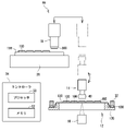
- FIG. 1 is a diagram showing the configuration of a manufacturing apparatus 10.
- the manufacturing apparatus 10 picks up the chip 100 from the dicing tape 130 and bonds it to the substrate 110 or another chip 100 to be bonded to manufacture a semiconductor device.
- a bonding material is provided on one surface of the chip 100, and the chip 100 is bonded to the bonding target by pressing the one surface against the bonding target.
- the surface of the chip 100 on which the bonding material is formed is referred to as the "bonding surface 102", and the opposite surface thereof is referred to as the "holding surface”.
- the joint surface 102 is illustrated with a thick line.
- the chip 100 When the chip 100 is bonded to the object to be bonded, the chip 100 may be heated so that the bonding material melts, but in this example, the chip 100 is bonded to the object to be bonded at room temperature without heating.
- room temperature bonding is bonding using atomic bonding or molecular bonding.
- the bonding surface 102 of the chip 100 of this example is required to maintain high quality.
- the manufacturing apparatus 10 has a mounting head 18 and a stage in order to bond the chip 100 to the bonding target.
- the stage 20 is a table on which the substrate 110 is placed.
- the mounting head 18 is arranged to face the stage 20, and suction-holds the holding surface of the chip 100 at its end. In other words, the mounting head 18 holds the chip 100 so that the mounting surface of the chip 100 faces the stage 20 .
- the mounting head 18 By moving the mounting head 18 relative to the stage 20, the chip 100 is pressed against the object to be bonded.
- the manufacturing apparatus 10 is further provided with a wafer holding device 12, a pickup device (hereinafter referred to as "PU device") 14, and an energy irradiation device 16.
- the wafer holding device 12 holds the wafer together with the dicing tape 130 .
- a dicing tape 130 is attached to the wafer in advance, and the wafer is diced into individual chips 100 . Therefore, a plurality of chips 100 are arranged on the surface of the dicing tape 130 .
- the dicing tape 130 has a base material 132 and an adhesive layer 134 as will be detailed later, and the individual chips 100 are held by the adhesive force of the adhesive layer 134 .
- a wafer ring 136 is attached to the dicing tape 130 so as to surround the wafer.
- the plurality of chips 100 are held by the dicing tape 130 in such a posture that the holding surfaces are in contact with the adhesive layer 134 and the bonding surfaces 102 face upward (so-called face-up posture).
- the wafer holding device 12 holds the dicing tape 130 while applying tension to the outside in the plane direction, and has an expand ring 30 and a ring retainer 32 .
- the expand ring 30 is a substantially tubular member having a through-hole formed therethrough in the axial direction, and a flange extending radially outward is provided at the lower end thereof.
- the inner diameter of this expand ring 30 is larger than the diameter of the wafer and smaller than the inner diameter of the wafer ring 136 .
- the dicing tape 130 is placed on this expand ring 30 . Also, the wafer ring 136 attached to the dicing tape 130 is pressed against the flange of the expand ring 30 by the ring retainer 32 and fixed. At this time, the dicing tape 130 covers the upper ends of the through holes of the expand ring 30, and the dicing tape 130 can be accessed from below through the through holes.
- the PU device 14 picks up the chip 100 from the dicing tape 130 in a face-up state, changes the posture to a face-down posture, and directly or indirectly delivers it to the mounting head 18 .
- the PU device 14 is arranged to face the joint surface 102 of the chip 100, and holds the joint surface 102 of the chip 100 to be picked up (hereinafter referred to as "target chip 100"). It has a PU head 40 . After picking up the target chip 100, the PU head 40 rotates 180 degrees to change the target chip 100 into a face-down posture. The PU device 14 hands over the target chip 100 in this face-down posture to the mounting head 18 .
- the target chip 100 is directly passed from the PU device 14 to the mounting head 18 in FIG. 1, it may be passed through another device.
- the energy irradiation device 16 is provided on the back side of the dicing tape 130, that is, on the opposite side of the PU device 14 with the dicing tape 130 interposed therebetween. This energy irradiation device 16 selectively irradiates energy toward the target chip 100 to locally reduce the adhesive force of the dicing tape 130 .
- the energy is selected according to the properties of the adhesive layer of dicing tape 130 . In this example, the energy is light, more specifically, ultraviolet rays.
- the energy irradiation device 16 may change the position and/or orientation of the energy generation source (eg, UV lamp), or may change the position and/or orientation of the energy generation source and the dicing tape 130 .
- the energy generation source eg, UV lamp
- a mask member may be provided to limit the irradiation area.
- the energy irradiation device 16 changes the energy irradiation position according to the position of the target chip 100 . The reason why such an energy irradiation device 16 is provided will be described later.
- the controller 22 controls driving of the mounting head 18, the PU device 14, and the energy irradiation device 16 described above.
- Controller 22 is physically a computer having processor 50 and memory 52 .
- the PU head 40 holds the joint surface 102 of the target chip 100 and picks it up. may be mechanically or chemically altered, degrading the quality of the mating surface 102 . This causes deterioration in bonding quality between the chip 100 and the object to be bonded.
- it is required to prevent mechanical contact between the PU head 40 and the bonding surface 102 .
- the PU head 40 is provided with a non-contact chuck 60 that holds the bonding surface 102 of the target chip 100 in a non-contact manner. Further, an energy irradiation device 16 is provided for reducing the adhesive strength of the dicing tape 130 by irradiating the target chip 100 with energy.
- the non-contact chuck 60 and the energy irradiation device 16 will be described in detail below.
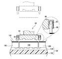
- FIG. 2 is a schematic diagram showing the configuration of the PU head 40.
- FIG. The PU head 40 of this example has the non-contact chuck 60 that holds the bonding surface 102 of the target chip 100 in a non-contact manner, as described above.
- the non-contact chuck 60 is formed with a plurality of ejection holes (not shown) for ejecting compressed air CA from substantially the center of the bottom surface (that is, the adsorption surface 62) toward the outside in the surface direction.
- a vacuum 64 is formed at substantially the center of the adsorption surface 62 by the compressed air CA flowing radially or cyclone-wise from the ejection holes along the adsorption surface 62 .
- the target chip 100 is attracted to the attraction surface 62 by bringing the attraction surface 62 close to the bonding surface 102 until the distance from the bonding surface 102 becomes equal to or less than a predetermined attraction distance.
- an air layer is formed by the compressed air CA flowing outward in the surface direction. This air layer prevents the joint surface 102 from contacting the adsorption surface 62 .
- the suction force generated by the formation of the vacuum 64 and the repulsive force generated by the air layer are simultaneously generated on the lower side of the adsorption surface 62 .
- the target chip 100 can be held without contact.
- the energy irradiation device 16 is provided in order to locally reduce the adhesive force of the dicing tape 130 .
- the dicing tape 130 handled in this example will be described.
- 3 to 5 are image diagrams showing pickup by the PU head 40.
- the dicing tape 130 is configured by laminating a base material 132 and an adhesive layer 134 .
- the adhesive layer 134 is a UV self-peeling adhesive layer from which the target chip 100 is automatically peeled off as it loses adhesiveness when irradiated with energy, more specifically, ultraviolet rays.
- a UV self-releasing adhesive layer can be composed, for example, of a special acrylic polymer and a UV-functional gas generant.
- the base material 132 may be made of a sheet made of a transparent resin such as polyacrylic, polyolefin, polycarbonate, vinyl chloride, ABS, polyethylene terephthalate (PET), nylon, polyurethane, polyimide, etc., as long as it can transmit ultraviolet rays. .
- the base material 132 may be composed of a sheet having a mesh structure, a sheet having holes, or the like.
- the target chip 100 When the area of the dicing tape 130 corresponding to the target chip 100 is irradiated with the ultraviolet rays 70 by the energy irradiation device 16, as shown in FIG. A gas is generated from the , and the target chip 100 is automatically peeled off. By separating the target chip 100 from the dicing tape 130 , the target chip 100 can be picked up even with a small suction force of the non-contact chuck 60 . Finally, the non-contact chuck 60 non-contactly holds and lifts the target chip 100 with an air layer interposed between the target chip 100 and the target chip 100, as shown in FIG.
- the non-contact chuck 60 can be used to pick up the target chip 100 by irradiating the adhesive layer 134 with energy to locally reduce the adhesive force.
- quality deterioration of the joint surface 102 can be effectively prevented, and the joint quality between the target chip 100 and the joint target can be further improved.
- the irradiation of the ultraviolet rays 70 by the energy irradiation device 16 starts at the same time as or after the non-contact chuck 60 starts blowing compressed air CA at a position close to the target chip 100 .
- This is to prevent the target chip 100 from jumping due to gas generated from the UV self-peeling adhesive layer.
- the adhesive layer 134 of the dicing tape 130 of this example is a UV self-peeling adhesive layer, and the UV self-peeling adhesive layer generates gas when irradiated with the ultraviolet rays 70 .
- the target chip 100 may jump off the dicing tape 130 due to the force of this gas ejection.
- the irradiation area Ea of the ultraviolet rays 70 (that is, energy) is an area that extends slightly outward from the outline of the target chip 100 so that the target chip 100 can be completely covered.
- the irradiation area Ea is an area that extends slightly outward from the outline of the target chip 100 so that the target chip 100 can be completely covered.
- the irradiation area Ea had to be slightly smaller than the external shape of the target chip 100 in order not to erroneously suck other adjacent chips 100 .
- the non-contact chuck 60 used in this example has a small suction force, even if the adhesive force of a part of the other chip 100 is reduced, the other chip 100 cannot be mistakenly sucked. do not have. Therefore, even if the irradiation area Ea is set larger than the target chip 100, there is no problem.
- the PU device 14 raises the PU head 40 when the target chip 100 is peeled off from the dicing tape 130 by irradiation with the ultraviolet rays 70 .
- the timing at which the target chip 100 is peeled off, and thus the timing at which the PU head 40 is lifted, may be determined from the elapsed time from the start of the irradiation of the ultraviolet rays 70, or from the change in the load acting on the PU head 40. good too. For example, the time required from the start of irradiation of the ultraviolet rays 70 to the peeling is obtained in advance as the peeling time as the peeling time. may be determined to be peeled off.
- the PU head 40 is provided with a detection unit 44 for detecting the load acting on the PU head 40, and the separation timing is determined based on the change in the load detected by the detection unit 44. can be judged. That is, when the non-contact chuck 60 is brought close to the target chip 100 while the compressed air CA is jetted, a vertically upward suction force Fa is generated in the target chip 100 (see FIGS. 3 and 4). When the target chip 100 is adhesively held by the adhesive layer 134 , the PU head 40 is acted upon by a vertically downward reaction force Fb that opposes the attraction force Fa. This reaction force Fb drops sharply at the timing when the target chip 100 is peeled off from the adhesive layer 134 .
- the detection unit 44 may detect this reaction force Fb and, in turn, the downward force acting on the PU head 40, and the timing at which the detected load suddenly drops may be determined as the peeling timing.
- the detection unit 44 may have a load sensor that detects the load acting on the PU head 40 .
- the detection unit 44 may be a mechanism that detects a downward force acting on the PU head 40 by monitoring the output of a motor capable of torque feedback that drives the PU head 40 .
- FIG. 6 is a flowchart showing the flow of pickup processing.
- the controller 22 first positions the PU head 40 (S10). That is, the PU head 40 is horizontally moved directly above the target chip 100, and the PU head 40 is lowered to move the PU head 40 to the target chip 100 up to the distance at which the suction force acts on the target chip 100, that is, the suction distance. bring close to
- the controller 22 supplies the compressed air CA to the non-contact chuck 60 of the PU head 40, and ejects the compressed air CA from the adsorption surface 62 (S12). Thereby, a vacuum 64 is formed under the non-contact chuck 60 and a suction force acts on the target chip 100 .
- the controller 22 starts irradiation of ultraviolet rays 70 by the energy irradiation device 16 (S14).
- the energy irradiation device 16 irradiates only the area corresponding to the target chip 100 with the ultraviolet rays 70 .
- the controller 22 continues irradiation of the ultraviolet rays 70 until a predetermined peeling time elapses from the irradiation of the ultraviolet rays 70 .
- the controller 22 determines that the target chip 100 has been peeled from the dicing tape 130.
- the load acting on the PU head 40 may be used to grasp the peeling timing.
- the controller 22 stops the irradiation of the ultraviolet rays 70 (S18) and raises the PU head 40 (S20). This completes the pickup of one target chip 100 .
- the PU device 14 delivers the picked up target chip 100 to the mounting head 18 as required. Also, if a new chip 100 needs to be picked up, steps S10 to S20 are repeated again.
- the target chip 100 can be picked up by the PU device 14 without coming into contact with the bonding surface 102 . It is possible to further improve the quality of bonding with the object to be bonded.
- the configuration described so far is only an example, and the PU device 14 that holds and picks up the target chip 100 in a non-contact manner and the target chip 100 are irradiated with energy in an area-selective manner to form a dicing tape 130.
- the energy irradiation device 16 that locally reduces the adhesive force is provided, other configurations may be changed as appropriate.
- the irradiation of the ultraviolet rays 70 is started after the compressed air CA is jetted.
- a pre-irradiation process may be performed to irradiate an amount of energy that maintains adhesive strength.
- the main irradiation treatment may be performed to irradiate energy in such an amount that the remaining adhesive strength disappears.
- the pre-irradiation process may be performed in advance on all of the plurality of chips 100 on the dicing tape 130 at one time. Further, as another form, while the PU device 14 is performing processing other than suction of the chip 100, for example, processing of transporting the chip 100 to the mounting head 18, a single pickup scheduled to be picked up next is performed. A pre-irradiation process may be performed on the chip 100 . By performing the pre-irradiation process in advance in this manner, the energy irradiation time in the main irradiation process can be shortened, and the time required for pickup can be shortened.
- the adhesive constituting the adhesive layer 134 may be a thermosetting adhesive that is crosslinked by heating to improve the elastic modulus and thereby reduce the adhesiveness, or a thermal foaming adhesive that contains a foaming agent that foams when heated.
- the compressed air CA when the compressed air CA is ejected from the non-contact chuck 60, wind is generated around the target chip 100, so the temperature of the target chip 100 and the surrounding dicing tape 130 tends to decrease. Therefore, if the compressed air CA is jetted in parallel with the heat irradiation, the temperature of the peeling layer may not rise sufficiently, and the peeling of the target chip 100 may be insufficient. Therefore, when heat is applied as energy, the compressed air CA may be ejected from the non-contact chuck 60 after peeling of the target chip 100 is completed, in other words, after heat irradiation is completed.
- FIG. 7 is a flowchart showing the flow of pick-up processing when irradiating heat.
- the thermal self-peeling dicing tape 130 is used, after positioning the PU head 40 (S30), heat irradiation is started prior to ejection of the compressed air CA (S36). (S32). Then, when a predetermined peeling time has passed (Yes in S34) and it can be judged that the peeling of the target chip 100 is completed, the injection of compressed air CA is started (S36), and the target chip 100 is held by the PU head 40 in a non-contact manner. do.
- the air ejection type non-contact chuck 60 that holds an object to be sucked in a non-contact manner by ejecting compressed air CA is used. good.
- an ultrasonic non-contact chuck 60 that uses high-frequency vibration to hold an object to be sucked in a non-contact manner may be used.
- FIG. 8 is a diagram showing the configuration of the ultrasonic non-contact chuck 60. As shown in FIG. The non-contact chuck 60 has a sonotrode 66 that micro-vibrates at a high frequency by applying a voltage. A so-called squeeze film 68 is formed on the lower surface of the non-contact chuck 60 by this slight vibration.
- This squeeze film 68 excludes the target chip 100 from contacting the attraction surface 62 .
- the non-contact chuck 60 also performs air suction in parallel with the formation of the squeeze film 68 . As a result, while the target chip 100 is attracted to the adsorption surface 62 , the squeeze film 68 inhibits contact with the adsorption surface 62 , so the non-contact chuck 60 can hold the target chip 100 without contact.
- the non-contact chuck 60 constrains the object to be sucked (target chip 100) in its axial direction, but in the direction of the sucking surface 62, it restrains the object to be sucked. do not restrain. Therefore, the target chip 100 sucked by the non-contact chuck 60 tends to move relatively easily in the surface direction of the sucking surface 62 .
- the PU head 40 may be provided with a restriction mechanism that restricts the movement of the target chip 100 in the planar direction.
- FIG. 9 is a diagram showing an example of a regulation mechanism.
- a restricting pin 80 that can advance and retreat in the axial direction is provided on the peripheral surface of the PU head 40 .
- the restricting pin 80 is biased downward by a spring 82 .
- the regulating pins 80 contact the bonding surface 102 of another chip 100 adjacent to the target chip 100 .
- the regulating pin 80 retreats upward against the biasing force of the spring 82 due to the reaction force received from the other chip 100 .
- the regulation pin 80 advances downward due to the biasing force of the spring.
- the lower end of the regulating pin 80 is lower than the upper surface (bonding surface 102 ) of the target chip 100 , and the regulating pin 80 is close to the peripheral surface of the target chip 100 . Therefore, even if the target chip 100 tries to move in the planar direction, the target chip 100 comes into contact with the regulating pin 80, and the target chip 100 is restricted from moving in the planar direction.
- the regulating pin 80 contacts the bonding surface 102 of another target chip 100 .
- the position of the regulating pin 80 is determined so that this contact does not degrade the bonding quality of the chip 100 to the bonding target. That is, even in the joint surface 102, the joint material to be joined to the object to be joined (for example, the electrode portion) is required to maintain high quality, but the area without the joint material may have a slight change in quality. , does not adversely affect the joint quality. Therefore, when the regulation pin 80 is provided, its position and size should be determined so as to make contact with a portion that does not affect the joint quality.
Landscapes
- Container, Conveyance, Adherence, Positioning, Of Wafer (AREA)
- Wire Bonding (AREA)
- Dicing (AREA)
- Health & Medical Sciences (AREA)
- Toxicology (AREA)
Priority Applications (8)
| Application Number | Priority Date | Filing Date | Title |
|---|---|---|---|
| PCT/JP2021/001678 WO2022157830A1 (ja) | 2021-01-19 | 2021-01-19 | 半導体装置の製造装置 |
| TW110143872A TW202230595A (zh) | 2021-01-19 | 2021-11-25 | 半導體裝置的製造裝置 |
| US18/012,944 US12131921B2 (en) | 2021-01-19 | 2021-12-13 | Manufacturing apparatus of semiconductor device |
| CN202180026419.2A CN115380369B (zh) | 2021-01-19 | 2021-12-13 | 半导体装置的制造装置 |
| JP2022577031A JP7523823B2 (ja) | 2021-01-19 | 2021-12-13 | 半導体装置の製造装置 |
| PCT/JP2021/045830 WO2022158166A1 (ja) | 2021-01-19 | 2021-12-13 | 半導体装置の製造装置 |
| KR1020237027642A KR102891252B1 (ko) | 2021-01-19 | 2021-12-13 | 반도체 장치의 제조장치 |
| TW111138141A TWI828355B (zh) | 2021-01-19 | 2022-10-07 | 半導體裝置的製造裝置 |
Applications Claiming Priority (1)
| Application Number | Priority Date | Filing Date | Title |
|---|---|---|---|
| PCT/JP2021/001678 WO2022157830A1 (ja) | 2021-01-19 | 2021-01-19 | 半導体装置の製造装置 |
Publications (1)
| Publication Number | Publication Date |
|---|---|
| WO2022157830A1 true WO2022157830A1 (ja) | 2022-07-28 |
Family
ID=82549593
Family Applications (2)
| Application Number | Title | Priority Date | Filing Date |
|---|---|---|---|
| PCT/JP2021/001678 Ceased WO2022157830A1 (ja) | 2021-01-19 | 2021-01-19 | 半導体装置の製造装置 |
| PCT/JP2021/045830 Ceased WO2022158166A1 (ja) | 2021-01-19 | 2021-12-13 | 半導体装置の製造装置 |
Family Applications After (1)
| Application Number | Title | Priority Date | Filing Date |
|---|---|---|---|
| PCT/JP2021/045830 Ceased WO2022158166A1 (ja) | 2021-01-19 | 2021-12-13 | 半導体装置の製造装置 |
Country Status (6)
| Country | Link |
|---|---|
| US (1) | US12131921B2 (https=) |
| JP (1) | JP7523823B2 (https=) |
| KR (1) | KR102891252B1 (https=) |
| CN (1) | CN115380369B (https=) |
| TW (2) | TW202230595A (https=) |
| WO (2) | WO2022157830A1 (https=) |
Families Citing this family (6)
| Publication number | Priority date | Publication date | Assignee | Title |
|---|---|---|---|---|
| KR20250105390A (ko) * | 2022-10-27 | 2025-07-08 | 도쿄엘렉트론가부시키가이샤 | 옮겨 싣기 장치, 기판 처리 장치, 옮겨 싣기 방법 및 기판 처리 방법 |
| KR20250105403A (ko) * | 2022-12-06 | 2025-07-08 | 파나소닉 아이피 매니지먼트 가부시키가이샤 | 픽업 시스템 및 픽업 방법 |
| TW202507896A (zh) * | 2023-08-03 | 2025-02-16 | 日商松下知識產權經營股份有限公司 | 拾取系統、接合裝置、分類裝置及拾取方法 |
| TW202520412A (zh) * | 2023-10-12 | 2025-05-16 | 日商松下知識產權經營股份有限公司 | 拾取系統、接合裝置、分類裝置及控制方法 |
| JP2025095916A (ja) * | 2023-12-15 | 2025-06-26 | ヤマハロボティクスホールディングス株式会社 | 半導体装置の製造装置および半導体装置の製造方法 |
| WO2025243968A1 (ja) * | 2024-05-22 | 2025-11-27 | パナソニックIpマネジメント株式会社 | 接合装置および制御方法 |
Citations (10)
| Publication number | Priority date | Publication date | Assignee | Title |
|---|---|---|---|---|
| JPH0272638A (ja) * | 1988-09-07 | 1990-03-12 | Seiko Epson Corp | 半導体装置の製造方法 |
| JP2001200234A (ja) * | 2000-01-21 | 2001-07-24 | Asahi Kasei Corp | 半導体ウエハー固定用の粘着剤ならびに加工方法 |
| JP2004072037A (ja) * | 2002-08-09 | 2004-03-04 | Renesas Technology Corp | 半導体装置の製造方法 |
| JP2006160935A (ja) * | 2004-12-09 | 2006-06-22 | Nitto Denko Corp | 被着物の加熱剥離方法及び被着物加熱剥離装置 |
| JP2006324373A (ja) * | 2005-05-18 | 2006-11-30 | Matsushita Electric Ind Co Ltd | チップのピックアップ装置およびピックアップ方法 |
| JP2007194433A (ja) * | 2006-01-19 | 2007-08-02 | Canon Machinery Inc | ピックアップ装置及びピックアップ方法 |
| JP2012199442A (ja) * | 2011-03-22 | 2012-10-18 | Hitachi High-Tech Instruments Co Ltd | ダイボンダ及び半導体製造方法 |
| WO2018061107A1 (ja) * | 2016-09-28 | 2018-04-05 | 富士機械製造株式会社 | ダイ実装装置 |
| WO2020213566A1 (ja) * | 2019-04-15 | 2020-10-22 | 株式会社新川 | 搬送装置 |
| WO2020213567A1 (ja) * | 2019-04-15 | 2020-10-22 | 株式会社新川 | 実装装置 |
Family Cites Families (11)
| Publication number | Priority date | Publication date | Assignee | Title |
|---|---|---|---|---|
| JP2008130742A (ja) | 2006-11-20 | 2008-06-05 | Sekisui Chem Co Ltd | 半導体チップの製造方法 |
| KR20140064255A (ko) * | 2012-11-20 | 2014-05-28 | 한미반도체 주식회사 | 전자부품 실장장치 및 이의 인포지션 판정 방법 |
| TWI553721B (zh) * | 2012-12-26 | 2016-10-11 | 日立化成股份有限公司 | 擴展方法、以及半導體裝置的製造方法 |
| US9437468B2 (en) * | 2014-03-29 | 2016-09-06 | Intel Corporation | Heat assisted handling of highly warped substrates post temporary bonding |
| DE102014111744B4 (de) * | 2014-08-18 | 2022-01-05 | Infineon Technologies Ag | Baugruppe zum handhaben eines halbleiterchips und verfahren zum handhaben eines halbleiterchips |
| JP6418360B1 (ja) * | 2017-03-17 | 2018-11-07 | 住友ベークライト株式会社 | 粘着テープセットおよび半導体素子移送用粘着テープ |
| JP6720333B2 (ja) * | 2017-06-12 | 2020-07-08 | ユニカルタ・インコーポレイテッド | 基板上に個別部品を並列に組み立てる方法 |
| KR102516339B1 (ko) * | 2018-04-06 | 2023-03-31 | 삼성전자주식회사 | 광 조사기용 덮개 구조물과 이를 구비하는 광 조사장치 및 이를 이용한 다이 접착 방법 |
| KR20190131311A (ko) * | 2018-05-16 | 2019-11-26 | (주)포인트엔지니어링 | 마이크로 led 흡착체 |
| KR102361476B1 (ko) * | 2019-06-25 | 2022-02-10 | 세메스 주식회사 | 반도체 소자들을 픽업하기 위한 장치 및 방법 |
| US11056377B2 (en) * | 2019-07-02 | 2021-07-06 | Asm Technology Singapore Pte Ltd | Collet inspection in a semiconductor pick and place apparatus |
-
2021
- 2021-01-19 WO PCT/JP2021/001678 patent/WO2022157830A1/ja not_active Ceased
- 2021-11-25 TW TW110143872A patent/TW202230595A/zh unknown
- 2021-12-13 WO PCT/JP2021/045830 patent/WO2022158166A1/ja not_active Ceased
- 2021-12-13 KR KR1020237027642A patent/KR102891252B1/ko active Active
- 2021-12-13 US US18/012,944 patent/US12131921B2/en active Active
- 2021-12-13 CN CN202180026419.2A patent/CN115380369B/zh active Active
- 2021-12-13 JP JP2022577031A patent/JP7523823B2/ja active Active
-
2022
- 2022-10-07 TW TW111138141A patent/TWI828355B/zh active
Patent Citations (10)
| Publication number | Priority date | Publication date | Assignee | Title |
|---|---|---|---|---|
| JPH0272638A (ja) * | 1988-09-07 | 1990-03-12 | Seiko Epson Corp | 半導体装置の製造方法 |
| JP2001200234A (ja) * | 2000-01-21 | 2001-07-24 | Asahi Kasei Corp | 半導体ウエハー固定用の粘着剤ならびに加工方法 |
| JP2004072037A (ja) * | 2002-08-09 | 2004-03-04 | Renesas Technology Corp | 半導体装置の製造方法 |
| JP2006160935A (ja) * | 2004-12-09 | 2006-06-22 | Nitto Denko Corp | 被着物の加熱剥離方法及び被着物加熱剥離装置 |
| JP2006324373A (ja) * | 2005-05-18 | 2006-11-30 | Matsushita Electric Ind Co Ltd | チップのピックアップ装置およびピックアップ方法 |
| JP2007194433A (ja) * | 2006-01-19 | 2007-08-02 | Canon Machinery Inc | ピックアップ装置及びピックアップ方法 |
| JP2012199442A (ja) * | 2011-03-22 | 2012-10-18 | Hitachi High-Tech Instruments Co Ltd | ダイボンダ及び半導体製造方法 |
| WO2018061107A1 (ja) * | 2016-09-28 | 2018-04-05 | 富士機械製造株式会社 | ダイ実装装置 |
| WO2020213566A1 (ja) * | 2019-04-15 | 2020-10-22 | 株式会社新川 | 搬送装置 |
| WO2020213567A1 (ja) * | 2019-04-15 | 2020-10-22 | 株式会社新川 | 実装装置 |
Also Published As
| Publication number | Publication date |
|---|---|
| TW202329297A (zh) | 2023-07-16 |
| TW202230595A (zh) | 2022-08-01 |
| US20230352324A1 (en) | 2023-11-02 |
| WO2022158166A1 (ja) | 2022-07-28 |
| JPWO2022158166A1 (https=) | 2022-07-28 |
| US12131921B2 (en) | 2024-10-29 |
| TWI828355B (zh) | 2024-01-01 |
| JP7523823B2 (ja) | 2024-07-29 |
| KR102891252B1 (ko) | 2025-12-03 |
| CN115380369B (zh) | 2025-09-12 |
| KR20230129542A (ko) | 2023-09-08 |
| CN115380369A (zh) | 2022-11-22 |
Similar Documents
| Publication | Publication Date | Title |
|---|---|---|
| WO2022157830A1 (ja) | 半導体装置の製造装置 | |
| JP5253996B2 (ja) | ワーク分割方法およびテープ拡張装置 | |
| CN102034747B (zh) | 保护带剥离方法及其装置 | |
| TWI463580B (zh) | Manufacturing method of semiconductor integrated circuit device | |
| KR100638760B1 (ko) | 반도체 장치 및 반도체 장치의 제조 방법 | |
| JP5612963B2 (ja) | 電子部品実装装置および電子部品実装方法 | |
| CN101409225B (zh) | 紫外线照射方法及使用了该方法的装置 | |
| US20170309594A1 (en) | Bonding method of semiconductor chip and bonding apparatus of semiconductor chip | |
| CN102005365B (zh) | 保护带剥离方法及其装置 | |
| JP2004304066A (ja) | 半導体装置の製造方法 | |
| WO2021039405A1 (ja) | 接合装置、接合システム、及び接合方法 | |
| JP2021153176A (ja) | ダイボンディング装置、剥離治具および半導体装置の製造方法 | |
| TW202105632A (zh) | 電子裝置的製造方法 | |
| JP2010219219A (ja) | 電子部品剥離装置及び電子部品剥離方法 | |
| JP4136692B2 (ja) | ペレット搬送装置、ペレットボンディング方法およびペレットボンディング装置 | |
| CN114999986A (zh) | 工件与片材的一体化方法及其一体化装置和半导体产品的制造方法 | |
| JP6200735B2 (ja) | ダイボンダ及びボンディング方法 | |
| JP5847410B2 (ja) | ダイボンダ及び半導体製造方法 | |
| KR20250026841A (ko) | 반도체 장치의 제조 장치 및 제조 방법 | |
| WO2004030079A1 (ja) | 接合方法および装置 | |
| JP2021111671A (ja) | ダイボンディング装置、半導体装置の製造方法およびエキスパンド装置 | |
| JP3243190B2 (ja) | 半導体装置の製造装置および製造方法 | |
| US20250300003A1 (en) | Frame unit forming method, frame unit forming apparatus, and method of forming device chips | |
| JP2007220905A (ja) | 板状物品のピックアップ装置 |
Legal Events
| Date | Code | Title | Description |
|---|---|---|---|
| 121 | Ep: the epo has been informed by wipo that ep was designated in this application |
Ref document number: 21920129 Country of ref document: EP Kind code of ref document: A1 |
|
| NENP | Non-entry into the national phase |
Ref country code: DE |
|
| 122 | Ep: pct application non-entry in european phase |
Ref document number: 21920129 Country of ref document: EP Kind code of ref document: A1 |
|
| NENP | Non-entry into the national phase |
Ref country code: JP |