WO2022118141A1 - 表示装置、および表示補正システム - Google Patents
表示装置、および表示補正システム Download PDFInfo
- Publication number
- WO2022118141A1 WO2022118141A1 PCT/IB2021/060902 IB2021060902W WO2022118141A1 WO 2022118141 A1 WO2022118141 A1 WO 2022118141A1 IB 2021060902 W IB2021060902 W IB 2021060902W WO 2022118141 A1 WO2022118141 A1 WO 2022118141A1
- Authority
- WO
- WIPO (PCT)
- Prior art keywords
- circuit
- layer
- insulator
- transistor
- conductor
- Prior art date
- Legal status (The legal status is an assumption and is not a legal conclusion. Google has not performed a legal analysis and makes no representation as to the accuracy of the status listed.)
- Ceased
Links
Images


























Classifications
-
- G—PHYSICS
- G09—EDUCATION; CRYPTOGRAPHY; DISPLAY; ADVERTISING; SEALS
- G09G—ARRANGEMENTS OR CIRCUITS FOR CONTROL OF INDICATING DEVICES USING STATIC MEANS TO PRESENT VARIABLE INFORMATION
- G09G3/00—Control arrangements or circuits, of interest only in connection with visual indicators other than cathode-ray tubes
- G09G3/20—Control arrangements or circuits, of interest only in connection with visual indicators other than cathode-ray tubes for presentation of an assembly of a number of characters, e.g. a page, by composing the assembly by combination of individual elements arranged in a matrix no fixed position being assigned to or needed to be assigned to the individual characters or partial characters
- G09G3/22—Control arrangements or circuits, of interest only in connection with visual indicators other than cathode-ray tubes for presentation of an assembly of a number of characters, e.g. a page, by composing the assembly by combination of individual elements arranged in a matrix no fixed position being assigned to or needed to be assigned to the individual characters or partial characters using controlled light sources
- G09G3/30—Control arrangements or circuits, of interest only in connection with visual indicators other than cathode-ray tubes for presentation of an assembly of a number of characters, e.g. a page, by composing the assembly by combination of individual elements arranged in a matrix no fixed position being assigned to or needed to be assigned to the individual characters or partial characters using controlled light sources using electroluminescent panels
- G09G3/32—Control arrangements or circuits, of interest only in connection with visual indicators other than cathode-ray tubes for presentation of an assembly of a number of characters, e.g. a page, by composing the assembly by combination of individual elements arranged in a matrix no fixed position being assigned to or needed to be assigned to the individual characters or partial characters using controlled light sources using electroluminescent panels semiconductive, e.g. using light-emitting diodes [LED]
- G09G3/3208—Control arrangements or circuits, of interest only in connection with visual indicators other than cathode-ray tubes for presentation of an assembly of a number of characters, e.g. a page, by composing the assembly by combination of individual elements arranged in a matrix no fixed position being assigned to or needed to be assigned to the individual characters or partial characters using controlled light sources using electroluminescent panels semiconductive, e.g. using light-emitting diodes [LED] organic, e.g. using organic light-emitting diodes [OLED]
- G09G3/3225—Control arrangements or circuits, of interest only in connection with visual indicators other than cathode-ray tubes for presentation of an assembly of a number of characters, e.g. a page, by composing the assembly by combination of individual elements arranged in a matrix no fixed position being assigned to or needed to be assigned to the individual characters or partial characters using controlled light sources using electroluminescent panels semiconductive, e.g. using light-emitting diodes [LED] organic, e.g. using organic light-emitting diodes [OLED] using an active matrix
- G09G3/3233—Control arrangements or circuits, of interest only in connection with visual indicators other than cathode-ray tubes for presentation of an assembly of a number of characters, e.g. a page, by composing the assembly by combination of individual elements arranged in a matrix no fixed position being assigned to or needed to be assigned to the individual characters or partial characters using controlled light sources using electroluminescent panels semiconductive, e.g. using light-emitting diodes [LED] organic, e.g. using organic light-emitting diodes [OLED] using an active matrix with pixel circuitry controlling the current through the light-emitting element
-
- G—PHYSICS
- G02—OPTICS
- G02B—OPTICAL ELEMENTS, SYSTEMS OR APPARATUS
- G02B27/00—Optical systems or apparatus not provided for by any of the groups G02B1/00 - G02B26/00, G02B30/00
- G02B27/02—Viewing or reading apparatus
-
- G—PHYSICS
- G09—EDUCATION; CRYPTOGRAPHY; DISPLAY; ADVERTISING; SEALS
- G09F—DISPLAYING; ADVERTISING; SIGNS; LABELS OR NAME-PLATES; SEALS
- G09F9/00—Indicating arrangements for variable information in which the information is built-up on a support by selection or combination of individual elements
- G09F9/30—Indicating arrangements for variable information in which the information is built-up on a support by selection or combination of individual elements in which the desired character or characters are formed by combining individual elements
-
- G—PHYSICS
- G09—EDUCATION; CRYPTOGRAPHY; DISPLAY; ADVERTISING; SEALS
- G09F—DISPLAYING; ADVERTISING; SIGNS; LABELS OR NAME-PLATES; SEALS
- G09F9/00—Indicating arrangements for variable information in which the information is built-up on a support by selection or combination of individual elements
- G09F9/30—Indicating arrangements for variable information in which the information is built-up on a support by selection or combination of individual elements in which the desired character or characters are formed by combining individual elements
- G09F9/33—Indicating arrangements for variable information in which the information is built-up on a support by selection or combination of individual elements in which the desired character or characters are formed by combining individual elements being semiconductor devices, e.g. diodes
- G09F9/335—Indicating arrangements for variable information in which the information is built-up on a support by selection or combination of individual elements in which the desired character or characters are formed by combining individual elements being semiconductor devices, e.g. diodes being organic light emitting diodes [OLED]
-
- G—PHYSICS
- G09—EDUCATION; CRYPTOGRAPHY; DISPLAY; ADVERTISING; SEALS
- G09G—ARRANGEMENTS OR CIRCUITS FOR CONTROL OF INDICATING DEVICES USING STATIC MEANS TO PRESENT VARIABLE INFORMATION
- G09G3/00—Control arrangements or circuits, of interest only in connection with visual indicators other than cathode-ray tubes
- G09G3/20—Control arrangements or circuits, of interest only in connection with visual indicators other than cathode-ray tubes for presentation of an assembly of a number of characters, e.g. a page, by composing the assembly by combination of individual elements arranged in a matrix no fixed position being assigned to or needed to be assigned to the individual characters or partial characters
- G09G3/22—Control arrangements or circuits, of interest only in connection with visual indicators other than cathode-ray tubes for presentation of an assembly of a number of characters, e.g. a page, by composing the assembly by combination of individual elements arranged in a matrix no fixed position being assigned to or needed to be assigned to the individual characters or partial characters using controlled light sources
- G09G3/30—Control arrangements or circuits, of interest only in connection with visual indicators other than cathode-ray tubes for presentation of an assembly of a number of characters, e.g. a page, by composing the assembly by combination of individual elements arranged in a matrix no fixed position being assigned to or needed to be assigned to the individual characters or partial characters using controlled light sources using electroluminescent panels
- G09G3/32—Control arrangements or circuits, of interest only in connection with visual indicators other than cathode-ray tubes for presentation of an assembly of a number of characters, e.g. a page, by composing the assembly by combination of individual elements arranged in a matrix no fixed position being assigned to or needed to be assigned to the individual characters or partial characters using controlled light sources using electroluminescent panels semiconductive, e.g. using light-emitting diodes [LED]
-
- H—ELECTRICITY
- H05—ELECTRIC TECHNIQUES NOT OTHERWISE PROVIDED FOR
- H05B—ELECTRIC HEATING; ELECTRIC LIGHT SOURCES NOT OTHERWISE PROVIDED FOR; CIRCUIT ARRANGEMENTS FOR ELECTRIC LIGHT SOURCES, IN GENERAL
- H05B33/00—Electroluminescent light sources
- H05B33/02—Details
-
- G—PHYSICS
- G09—EDUCATION; CRYPTOGRAPHY; DISPLAY; ADVERTISING; SEALS
- G09G—ARRANGEMENTS OR CIRCUITS FOR CONTROL OF INDICATING DEVICES USING STATIC MEANS TO PRESENT VARIABLE INFORMATION
- G09G2300/00—Aspects of the constitution of display devices
- G09G2300/02—Composition of display devices
- G09G2300/023—Display panel composed of stacked panels
-
- G—PHYSICS
- G09—EDUCATION; CRYPTOGRAPHY; DISPLAY; ADVERTISING; SEALS
- G09G—ARRANGEMENTS OR CIRCUITS FOR CONTROL OF INDICATING DEVICES USING STATIC MEANS TO PRESENT VARIABLE INFORMATION
- G09G2300/00—Aspects of the constitution of display devices
- G09G2300/04—Structural and physical details of display devices
- G09G2300/0404—Matrix technologies
-
- G—PHYSICS
- G09—EDUCATION; CRYPTOGRAPHY; DISPLAY; ADVERTISING; SEALS
- G09G—ARRANGEMENTS OR CIRCUITS FOR CONTROL OF INDICATING DEVICES USING STATIC MEANS TO PRESENT VARIABLE INFORMATION
- G09G2300/00—Aspects of the constitution of display devices
- G09G2300/04—Structural and physical details of display devices
- G09G2300/0404—Matrix technologies
- G09G2300/0417—Special arrangements specific to the use of low carrier mobility technology
-
- G—PHYSICS
- G09—EDUCATION; CRYPTOGRAPHY; DISPLAY; ADVERTISING; SEALS
- G09G—ARRANGEMENTS OR CIRCUITS FOR CONTROL OF INDICATING DEVICES USING STATIC MEANS TO PRESENT VARIABLE INFORMATION
- G09G2300/00—Aspects of the constitution of display devices
- G09G2300/04—Structural and physical details of display devices
- G09G2300/0421—Structural details of the set of electrodes
- G09G2300/0426—Layout of electrodes and connections
-
- G—PHYSICS
- G09—EDUCATION; CRYPTOGRAPHY; DISPLAY; ADVERTISING; SEALS
- G09G—ARRANGEMENTS OR CIRCUITS FOR CONTROL OF INDICATING DEVICES USING STATIC MEANS TO PRESENT VARIABLE INFORMATION
- G09G2300/00—Aspects of the constitution of display devices
- G09G2300/04—Structural and physical details of display devices
- G09G2300/0439—Pixel structures
- G09G2300/0452—Details of colour pixel setup, e.g. pixel composed of a red, a blue and two green components
-
- G—PHYSICS
- G09—EDUCATION; CRYPTOGRAPHY; DISPLAY; ADVERTISING; SEALS
- G09G—ARRANGEMENTS OR CIRCUITS FOR CONTROL OF INDICATING DEVICES USING STATIC MEANS TO PRESENT VARIABLE INFORMATION
- G09G2300/00—Aspects of the constitution of display devices
- G09G2300/08—Active matrix structure, i.e. with use of active elements, inclusive of non-linear two terminal elements, in the pixels together with light emitting or modulating elements
- G09G2300/0809—Several active elements per pixel in active matrix panels
- G09G2300/0814—Several active elements per pixel in active matrix panels used for selection purposes, e.g. logical AND for partial update
-
- G—PHYSICS
- G09—EDUCATION; CRYPTOGRAPHY; DISPLAY; ADVERTISING; SEALS
- G09G—ARRANGEMENTS OR CIRCUITS FOR CONTROL OF INDICATING DEVICES USING STATIC MEANS TO PRESENT VARIABLE INFORMATION
- G09G2300/00—Aspects of the constitution of display devices
- G09G2300/08—Active matrix structure, i.e. with use of active elements, inclusive of non-linear two terminal elements, in the pixels together with light emitting or modulating elements
- G09G2300/0809—Several active elements per pixel in active matrix panels
- G09G2300/0842—Several active elements per pixel in active matrix panels forming a memory circuit, e.g. a dynamic memory with one capacitor
-
- G—PHYSICS
- G09—EDUCATION; CRYPTOGRAPHY; DISPLAY; ADVERTISING; SEALS
- G09G—ARRANGEMENTS OR CIRCUITS FOR CONTROL OF INDICATING DEVICES USING STATIC MEANS TO PRESENT VARIABLE INFORMATION
- G09G2300/00—Aspects of the constitution of display devices
- G09G2300/08—Active matrix structure, i.e. with use of active elements, inclusive of non-linear two terminal elements, in the pixels together with light emitting or modulating elements
- G09G2300/0809—Several active elements per pixel in active matrix panels
- G09G2300/0842—Several active elements per pixel in active matrix panels forming a memory circuit, e.g. a dynamic memory with one capacitor
- G09G2300/0861—Several active elements per pixel in active matrix panels forming a memory circuit, e.g. a dynamic memory with one capacitor with additional control of the display period without amending the charge stored in a pixel memory, e.g. by means of additional select electrodes
-
- G—PHYSICS
- G09—EDUCATION; CRYPTOGRAPHY; DISPLAY; ADVERTISING; SEALS
- G09G—ARRANGEMENTS OR CIRCUITS FOR CONTROL OF INDICATING DEVICES USING STATIC MEANS TO PRESENT VARIABLE INFORMATION
- G09G2310/00—Command of the display device
- G09G2310/02—Addressing, scanning or driving the display screen or processing steps related thereto
- G09G2310/0264—Details of driving circuits
- G09G2310/0289—Details of voltage level shifters arranged for use in a driving circuit
-
- G—PHYSICS
- G09—EDUCATION; CRYPTOGRAPHY; DISPLAY; ADVERTISING; SEALS
- G09G—ARRANGEMENTS OR CIRCUITS FOR CONTROL OF INDICATING DEVICES USING STATIC MEANS TO PRESENT VARIABLE INFORMATION
- G09G2310/00—Command of the display device
- G09G2310/08—Details of timing specific for flat panels, other than clock recovery
-
- G—PHYSICS
- G09—EDUCATION; CRYPTOGRAPHY; DISPLAY; ADVERTISING; SEALS
- G09G—ARRANGEMENTS OR CIRCUITS FOR CONTROL OF INDICATING DEVICES USING STATIC MEANS TO PRESENT VARIABLE INFORMATION
- G09G2320/00—Control of display operating conditions
- G09G2320/02—Improving the quality of display appearance
- G09G2320/0233—Improving the luminance or brightness uniformity across the screen
-
- G—PHYSICS
- G09—EDUCATION; CRYPTOGRAPHY; DISPLAY; ADVERTISING; SEALS
- G09G—ARRANGEMENTS OR CIRCUITS FOR CONTROL OF INDICATING DEVICES USING STATIC MEANS TO PRESENT VARIABLE INFORMATION
- G09G2320/00—Control of display operating conditions
- G09G2320/02—Improving the quality of display appearance
- G09G2320/029—Improving the quality of display appearance by monitoring one or more pixels in the display panel, e.g. by monitoring a fixed reference pixel
- G09G2320/0295—Improving the quality of display appearance by monitoring one or more pixels in the display panel, e.g. by monitoring a fixed reference pixel by monitoring each display pixel
-
- G—PHYSICS
- G09—EDUCATION; CRYPTOGRAPHY; DISPLAY; ADVERTISING; SEALS
- G09G—ARRANGEMENTS OR CIRCUITS FOR CONTROL OF INDICATING DEVICES USING STATIC MEANS TO PRESENT VARIABLE INFORMATION
- G09G2320/00—Control of display operating conditions
- G09G2320/06—Adjustment of display parameters
- G09G2320/0626—Adjustment of display parameters for control of overall brightness
-
- G—PHYSICS
- G09—EDUCATION; CRYPTOGRAPHY; DISPLAY; ADVERTISING; SEALS
- G09G—ARRANGEMENTS OR CIRCUITS FOR CONTROL OF INDICATING DEVICES USING STATIC MEANS TO PRESENT VARIABLE INFORMATION
- G09G2330/00—Aspects of power supply; Aspects of display protection and defect management
- G09G2330/02—Details of power systems and of start or stop of display operation
- G09G2330/021—Power management, e.g. power saving
-
- G—PHYSICS
- G09—EDUCATION; CRYPTOGRAPHY; DISPLAY; ADVERTISING; SEALS
- G09G—ARRANGEMENTS OR CIRCUITS FOR CONTROL OF INDICATING DEVICES USING STATIC MEANS TO PRESENT VARIABLE INFORMATION
- G09G2330/00—Aspects of power supply; Aspects of display protection and defect management
- G09G2330/08—Fault-tolerant or redundant circuits, or circuits in which repair of defects is prepared
-
- G—PHYSICS
- G09—EDUCATION; CRYPTOGRAPHY; DISPLAY; ADVERTISING; SEALS
- G09G—ARRANGEMENTS OR CIRCUITS FOR CONTROL OF INDICATING DEVICES USING STATIC MEANS TO PRESENT VARIABLE INFORMATION
- G09G2330/00—Aspects of power supply; Aspects of display protection and defect management
- G09G2330/10—Dealing with defective pixels
Definitions
- One embodiment of the present invention relates to a display device and a display correction system.
- one aspect of the present invention is not limited to the above technical fields.
- the technical fields of one aspect of the present invention disclosed in the present specification and the like include semiconductor devices, image pickup devices, display devices, light emitting devices, power storage devices, storage devices, display systems, electronic devices, lighting devices, input devices, and input / output devices.
- Devices, their driving methods, or their manufacturing methods can be mentioned as an example.
- the semiconductor device refers to all devices that can function by utilizing the semiconductor characteristics.
- Display devices liquid crystal display devices, light emission display devices, etc.
- projection devices lighting devices, electro-optic devices, power storage devices, storage devices, semiconductor circuits, image pickup devices, electronic devices, and the like may be said to be semiconductor devices.
- they may be said to have semiconductor devices.
- Wearable electronic devices and stationary electronic devices are becoming widespread as electronic devices provided with display devices for augmented reality (AR) or virtual reality (VR).
- Examples of the wearable type electronic device include a head-mounted display (HMD: Head Mounted Display), a spectacle-type electronic device, and the like.
- Examples of the stationary electronic device include a head-up display (HUD: Head-Up Display) and the like.
- Patent Document 1 discloses a method of realizing an HMD having fine pixels by using a transistor capable of high-speed driving.
- the pixel density can be increased by making the pixels of the display device fine. As a result, a large number of pixels can be provided in the display device, and a high immersive feeling or a realistic feeling can be obtained. In order to obtain a more immersive or realistic feeling, it is preferable that there are few pixel defects (bright spots, dark spots, etc.).
- an arithmetic unit such as a CPU and a display device
- the function of the display device may be impaired due to heat generation of the arithmetic unit or the like.
- the degree of freedom in arranging the arithmetic unit may be impaired depending on the shape of the display device and the like.
- One of the problems of one embodiment of the present invention is to provide a display device having a new configuration, a display correction system, or the like.
- one of the problems of the present invention is to provide a display device, a display correction system, or the like that can be miniaturized.
- one of the problems of the present invention is to provide a display device, a display correction system, or the like that can reduce power consumption.
- one of the problems of the present invention is to provide a display device, a display correction system, or the like with an increased degree of freedom in the arrangement of arithmetic units.
- One aspect of the present invention includes a pixel circuit, a drive circuit, and a functional circuit
- the drive circuit has a function of outputting a signal for displaying in the pixel circuit
- the functional circuit is a backup circuit. It has a CPU with a CPU core having a flip-flop electrically connected to it, and has a first layer and a second layer, the first layer being a drive circuit, a CPU, and the like.
- the second layer has a pixel circuit and a backup circuit, and the first layer and the second layer are display devices provided in different layers.
- One aspect of the present invention includes a pixel circuit, a drive circuit, and a functional circuit, the drive circuit has a function of outputting an image signal for display in the pixel circuit, and the functional circuit is a backup. It has a CPU with a CPU core having a flip-flop electrically connected to the circuit, has a first layer, a second layer, and the first layer is a drive circuit and a CPU. , The second layer has a pixel circuit and a backup circuit, the first layer and the second layer are provided in different layers, and the CPU flows through the pixel circuit. It is a display device having a function of correcting an image signal according to the amount of current.
- the drive circuit has a function of outputting an image signal for display in the pixel circuit, and the functional circuit is a backup. It has a CPU with a CPU core having a flip flop electrically connected to the circuit, has a first layer, a second layer, and the first layer is a drive circuit and a CPU.
- the second layer has a pixel circuit and a backup circuit, and the first layer has a first transistor having a semiconductor layer having silicon in a channel forming region, and a second layer.
- the layer has a second transistor having a semiconductor layer having a metal oxide in the channel forming region, and the CPU is a display device having a function of correcting an image signal according to the amount of current flowing through the pixel circuit.
- the metal oxide is preferably a display device containing In, the element M (M is Al, Ga, Y, or Sn), and Zn.
- the backup circuit is preferably a display device having a function of holding the data held in the flip-flop in a state where the supply of the power supply voltage is stopped when the CPU is not operating.
- a display device is preferable in which the functional circuit has an accelerator and the accelerator is a circuit that performs a product-sum operation.
- the pixel circuit has an organic EL device, and the organic EL device is preferably a display device which is a light emitting device processed by a photolithography method.
- the backup circuit has a first transistor provided in the first layer and a capacitance electrically connected to the first transistor, the capacitance being provided in the first layer. Display devices are preferred.
- One aspect of the present invention includes a pixel circuit, a drive circuit, and a functional circuit, the drive circuit has a function of outputting an image signal for display in the pixel circuit, and the functional circuit is a backup. It has a CPU with a CPU core having a flip flop electrically connected to the circuit, has a first layer, a second layer, and the first layer is a drive circuit and a CPU. The second layer has a pixel circuit and a backup circuit, and the backup circuit turns off the first transistor having a semiconductor layer having silicon in the channel forming region when the CPU is not operating.
- the CPU has a function of holding the data possessed by the flip flop by setting it to a state, and the CPU has a function of correcting an image signal by estimating a defective pixel according to the amount of current flowing through the pixel circuit.
- This is a display correction system that corrects the amount of current flowing in the pixel circuit of a pixel adjacent to a defective pixel.
- One embodiment of the present invention can provide a display device having a new configuration, a display correction system, or the like.
- one embodiment of the present invention can provide a display device that can be miniaturized, a display correction system, or the like.
- one embodiment of the present invention can provide a display device, a display correction system, or the like that can reduce power consumption.
- one embodiment of the present invention can provide a display device having an increased degree of freedom in the arrangement of arithmetic units, a display correction system, or the like.
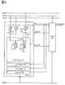
- FIG. 1 is a block diagram showing a configuration example of a display device.
- FIG. 2 is a block diagram showing a configuration example of the display device.
- FIG. 3 is a block diagram showing a configuration example of the display device.
- 4A and 4B are block diagrams showing a configuration example of a display device.
- FIG. 5 is a block diagram showing a configuration example of the display device.
- FIG. 6 is a block diagram showing a configuration example of the display device.
- 7A and 7B are circuit diagrams showing a configuration example of the display device.
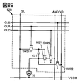
- 8A and 8B are circuit diagrams showing a configuration example of the display device.
- FIG. 9 is a block diagram showing a configuration example of the display device.
- 10A and 10B are circuit diagrams showing a configuration example of the display device.
- FIG. 11 is a timing chart showing an example of a driving method of the display device.
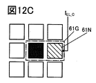
- 12A to 12C are a circuit diagram and a schematic diagram showing a configuration example of the display device.
- FIG. 13 is a block diagram showing a configuration example of the display device.
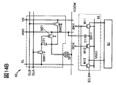
- 14A and 14B are circuit diagrams showing a configuration example of the display device.
- 15A and 15B are circuit diagrams showing a configuration example of a display device.
- FIG. 16 is a circuit diagram showing a configuration example of the display device.
- FIG. 17 is a circuit diagram showing a configuration example of the display device.
- FIG. 18 is a circuit diagram showing a configuration example of the display device.
- FIG. 19 is a circuit diagram showing a configuration example of the display device.
- 20A and 20B are circuit diagrams showing a configuration example of the display device.
- 21A and 21B are circuit diagrams showing a configuration example of a display device.
- 22A and 22B are circuit diagrams showing a configuration example of the display device.
- 23A and 23B are circuit diagrams showing a configuration example of the display device.
- 24A and 24B are circuit diagrams showing a configuration example of the display device.
- 25A and 25B are circuit diagrams showing a configuration example of the display device.
- 26A and 26B are circuit diagrams showing a configuration example of a display device.
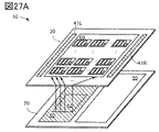
- 27A and 27B are block diagrams showing a configuration example of a display device.
- FIG. 28 is a cross-sectional view showing a configuration example of the display device.
- FIG. 29 is a cross-sectional view showing a configuration example of the display device.
- FIG. 30A is a block diagram showing a configuration example of the display device.
- FIG. 30B is a cross-sectional view showing a configuration example of the display device.
- FIG. 31 is a cross-sectional view showing a configuration example of the display device.
- FIG. 32 is a cross-sectional view showing a configuration example of the display device.
- FIG. 33 is a cross-sectional view showing a configuration example of the display device.
- FIG. 34 is a cross-sectional view showing a configuration example of the display device.
- FIG. 35A is a top view showing a configuration example of the transistor.
- 35B and 35C are cross-sectional views showing a configuration example of a transistor.
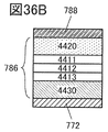
- 36A to 36C are views showing a configuration example of a display device.
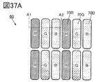
- FIG. 37A to 37C are views showing a configuration example of a display device.
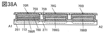
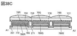
- 38A to 38C are views showing a configuration example of the display device.
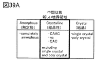
- FIG. 39A is a diagram illustrating the classification of the crystal structure of IGZO.
- FIG. 39B is a diagram illustrating an XRD spectrum of a CAAC-IGZO film.
- FIG. 39C is a diagram illustrating a microelectron beam diffraction pattern of the CAAC-IGZO film.
- 40A and 40B are diagrams showing an example of a display IC.
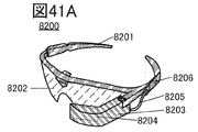
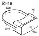
- 41A to 41D are views showing an example of an electronic device.
- 42A and 42B are diagrams showing an example of an electronic device.
- the off current means a drain current when the transistor is in an off state (also referred to as a non-conducting state or a cutoff state).
- the off state is a state in which the voltage V gs between the gate and the source is lower than the threshold voltage V th in the n-channel transistor (higher than V th in the p-channel transistor) unless otherwise specified. To say.
- a metal oxide is a metal oxide in a broad sense. Metal oxides are classified into oxide insulators, oxide conductors (including transparent oxide conductors), oxide semiconductors (also referred to as Oxide Semiconductor or simply OS) and the like. For example, when a metal oxide is used for the active layer of a transistor, the metal oxide may be referred to as an oxide semiconductor. That is, when it is described as an OS transistor, it can be rephrased as a transistor having an oxide or an oxide semiconductor.
- FIG. 1 is a block diagram schematically showing a configuration example of a display device 10 which is a display device of one aspect of the present invention.
- the display device 10 has a layer 20 and a layer 30, and the layer 30 can be provided so as to be laminated on, for example, above the layer 20.
- an interlayer insulator Between the layer 20 and the layer 30, an interlayer insulator, a conductor for making an electrical connection between different layers, and the like can be provided.
- the transistor provided in the layer 20 can be, for example, a transistor having silicon in the channel forming region (also referred to as a Si transistor), and can be, for example, a transistor having single crystal silicon in the channel forming region.
- a transistor having single crystal silicon in the channel forming region is used as the transistor provided in the layer 20
- the on-current of the transistor can be increased. Therefore, the circuit included in the layer 20 can be driven at high speed, which is preferable.
- the Si transistor can be formed by fine processing having a channel length of 3 nm to 10 nm, it can be a display device 10 provided with an accelerator such as a CPU and a GPU, an application processor, and the like.
- the transistor provided in the layer 30 can be, for example, an OS transistor.
- the OS transistor it is preferable to use a transistor having an oxide containing at least one of indium, element M (element M is aluminum, gallium, yttrium, or tin) and zinc in the channel forming region.
- Such an OS transistor has a characteristic that the off-current is very low. Therefore, it is particularly preferable to use an OS transistor as a transistor provided in the pixel circuit of the display unit because the analog data written in the pixel circuit can be retained for a long period of time.
- the drive circuit 40 and the functional circuit 50 are provided on the layer 20.
- the Si transistor of the layer 20 can increase the on-current of the transistor. Therefore, each circuit can be driven at high speed.
- the layer 30 is provided with a display unit 60 provided with a plurality of pixels 61.
- the pixel 61 is provided with pixel circuits 62R, 62G, 62B in which light emission of red, green, and blue is controlled.
- the pixel circuits 62R, 62G, and 62B have a function as sub-pixels of the pixel 61. Since the pixel circuits 62R, 62G, and 62B have an OS transistor, the analog data written in the pixel circuit can be held for a long period of time.
- a backup circuit 82 is provided for each of the pixels 61 of the layer 30.
- the backup circuit may be referred to as a storage circuit or a memory circuit.
- the drive circuit 40 includes a gate line drive circuit, a source line drive circuit, and the like for driving the pixel circuits 62R, 62G, and 62B.
- the drive circuit 40 includes a gate line drive circuit and a source line drive circuit for driving the pixel 61 of the display unit 60.
- the drive circuit 40 includes an LVDS (Low Voltage Differential Signaling) circuit having a function as an interface for receiving data such as image data from the outside of the display device 10, a D / A (Digital to Analog) conversion circuit, or the like. You may have.
- the Si transistor of the layer 20 can increase the on-current of the transistor.
- the channel length or channel width of the Si transistor may be different depending on the operating speed of each circuit.
- the functional circuit 50 has a CPU used for data calculation processing.
- the CPU has a plurality of CPU cores.
- the CPU core has a flip-flop.
- the flip-flop has a plurality of scan flip-flops.
- the flip-flop 80 inputs / outputs scan flip-flop data (backup data) to / from the backup circuit 82.
- a backup data BD is illustrated as a data signal held by the backup circuit 82.
- a memory having an OS transistor is suitable for the backup circuit 82.
- the backup circuit composed of OS transistors can suppress the voltage drop according to the data to be backed up due to the feature of OS transistor that the off current is extremely small, and it consumes almost no power to hold the data. , Etc. have advantages.
- the backup circuit 82 having an OS transistor can be provided in the display unit 60 in which a plurality of pixels 61 are arranged.
- FIG. 1 illustrates how a backup circuit 82 is provided in each pixel 61.
- the backup circuit 82 composed of the OS transistor can be provided by being laminated with the layer 20 having the Si transistor.
- the backup circuit 82 may be arranged in a matrix like the sub-pixels in the pixel 61, or may be arranged for each of a plurality of pixels. That is, the backup circuit 82 can be arranged in the layer 30 without being restricted by the arrangement of the pixels 61. Therefore, the degree of freedom of the display unit / circuit layout can be increased, the circuit area can be arranged without increasing the circuit area, and the storage capacity of the backup circuit 82 required for the arithmetic processing can be increased.
- ⁇ Configuration example of pixel circuit and backup circuit> 2 to 4 show a configuration example of the arrangement of the backup circuit 82 and the pixel circuits 62R, 62G, 62B which are sub-pixels in the display unit 60.
- FIG. 2 illustrates a configuration in which a plurality of pixels 61 are arranged in a matrix in the display unit 60.
- the pixel 61 has a backup circuit 82 in addition to the pixel circuits 62R, 62G, and 62B.
- the backup circuit 82 and the pixel circuits 62R, 62G, and 62B can all be configured by the OS transistor, they can be arranged in the same pixel.
- FIG. 3 illustrates a configuration in which a plurality of pixels 61 are arranged in a matrix in the display unit 60, and in FIG. 3, the pixels 61 in 2 rows and 2 columns are shown as unit pixels 61UNI.
- the pixel 61 has pixel circuits 62R, 62G, 62B.
- the unit pixel 61UNI has a backup circuit 82 at a position surrounded by four pixels 61. As described above, both the backup circuit 82 and the pixel 61 can be configured by the OS transistor, so that they can be arranged in the same unit pixel 61UNI.
- FIG. 4A illustrates a configuration in which pixels 61PEN to which the pentile arrangement is applied are arranged in the display unit.
- the pixel 61PEN has a backup circuit 82 in addition to the pixel circuits 62R and 62G or the pixel circuits 62B and 62G.
- the backup circuit 82 and the pixel circuits 62R, 62G, or the pixel circuits 62B, 62G can both be configured by the OS transistor, so that they can be arranged in the same pixel.
- FIG. 4B illustrates a configuration in which pixels 61PENs are arranged in a matrix in the display unit 60, and FIG. 4B illustrates pixels 61PENs in 2 rows and 2 columns as unit pixels 61UNI.
- the pixel 61PEN has a pixel circuit 62R, 62G, or a pixel circuit 62B, 62G.
- the unit pixel 61UNI has a backup circuit 82 at a position surrounded by four pixels 61PEN. As described above, both the backup circuit 82 and the pixel 61PEN can be configured by the OS transistor, so that they can be arranged in the same unit pixel 61UNI.
- FIG. 5 shows a block diagram for explaining each configuration of the display device 10.
- the display device includes a drive circuit 40, a functional circuit 50, and a display unit 60.
- the drive circuit 40 has a gate driver 41 and a source driver 42 as an example.
- the gate driver 41 has a function of driving a wiring GL that functions as a gate line for outputting a signal to the pixel circuits 62R, 62G, and 62B.
- the source driver 42 has a function of driving a plurality of wiring SLs that function as source lines for outputting signals to the pixel circuits 62R, 62G, and 62B. Further, the drive circuit 40 supplies a voltage for displaying in the pixel circuits 62R, 62G, 62B to the pixel circuits 62R, 62G, 62B via a plurality of wirings.
- the functional circuit 50 has a CPU 51.
- the CPU 51 has a CPU core 53.
- the CPU core 53 has a flip-flop 80 for temporarily holding data used for arithmetic processing.
- the flip-flop 80 has a plurality of scan flip-flops 81, and each scan flip-flop 81 is electrically connected to a backup circuit 82 provided in the display unit 60.
- the display unit 60 has a plurality of pixels 61 provided with pixel circuits 62R, 62G, 62B and a backup circuit 82.
- the backup circuit 82 does not necessarily have to be arranged in the pixel 61 which is a repeating unit. It can be freely arranged according to the shape of the display unit 60, the shapes of the pixel circuits 62R, 62G, 62B, and the like.
- FIG. 6 is a schematic diagram for explaining the positional relationship between the layer 30 provided on the layer 20 and the light emitting element 70.
- FIG. 6 corresponds to an example of a schematic cross-sectional view of the display device 10 shown in FIG.
- the functional circuits 50A and 50B are illustrated on the layer 20 as an example of the drive circuit 40 and the functional circuit 50.
- the drive circuit 40 and the functional circuits 50A and 50B have Si transistors.
- the functional circuits 50A and 50B are functional circuits having different functions.
- the layer 30 has pixel circuits 62R, 62G, 62B, and a backup circuit 82 provided at positions overlapping with the drive circuit 40, the functional circuits 50A, and 50B.
- FIG. 6 illustrates a configuration example having a backup circuit for each pixel circuit.
- the light emitting element 70 has light emitting elements 70R, 70G, 70B connected to the pixel circuits 62R, 62G, 62B, respectively.
- the light emitting element 70R, the pixel circuit 62R, the backup circuit 82, and the drive circuit 40 are provided so as to overlap each other in the region 71.
- the functional circuit 50A and the functional circuit 50B are connected to different backup circuits 82 via the wirings 72 and 73.
- the pixel circuits 62R, 62G, and 62B are connected to the light emitting elements 70R, 70G, and 70B, respectively, via the wiring 74.
- the backup circuit 82 can be provided on the layer 30 in which the OS transistor is provided, the backup circuit 82 can be provided in a laminated manner with the layer 20 having the Si transistor.
- the backup circuit 82 can be arranged in the layer 30 without being restricted by the arrangement of the pixels 61. Therefore, the degree of freedom of the display unit / circuit layout can be increased, the circuit area can be arranged without increasing the circuit area, and the storage capacity of the backup circuit 82 required for the arithmetic processing can be increased.
- the functional circuit 50A and the functional circuit 50B can be operated intermittently, so that power saving can be achieved.
- FIG. 7A and 7B show a configuration example of the pixel circuit 62 applicable to the pixel circuits 62R, 62G, and 62B, and a light emitting element 70 connected to the pixel circuit 62.
- FIG. 7A is a diagram showing the connection of each element
- FIG. 7B is a diagram schematically showing the vertical relationship between the drive circuit 40, the pixel circuit 62, and the light emitting element 70.
- the term element may be paraphrased as "device".
- the display element, the light emitting element, and the liquid crystal element can be paraphrased as, for example, a display device, a light emitting device, and a liquid crystal device.
- the pixel circuit 62 shown as an example in FIGS. 7A and 7B includes a switch SW21, a switch SW22, a transistor M21, and a capacitance C21.
- the switch SW21 and the switch SW22 can be transistors.
- the switch SW21 and the switch of the switch SW22 may also be transistors.
- the switch SW21, the switch SW22, and the transistor M21 can be composed of an OS transistor.
- Each OS transistor of the switch SW21, the switch SW22, and the transistor M21 is preferably provided with a back gate electrode.
- the back gate electrode is configured to give the same signal as the gate electrode, and the back gate electrode has a signal different from the gate electrode. Can be configured to give.
- the transistor M21 includes a gate electrode electrically connected to the switch SW21, a first electrode electrically connected to the light emitting element 70, and a second electrode electrically connected to the wiring ANO. ..
- the wiring ANO is wiring for giving a potential for supplying a current to the light emitting element 70.
- the switch SW21 has a first terminal electrically connected to the gate electrode of the transistor M21 and a second terminal electrically connected to the wiring SL functioning as a source line, and functions as a gate line. It has a function of controlling a conduction state or a non-conduction state based on the potential of the wiring GLA to be connected.
- the switch SW22 has a first terminal electrically connected to the wiring V0 and a second terminal electrically connected to the light emitting element 70, and is based on the potential of the wiring GLB which functions as a gate line. It also has a function to control the conduction state or the non-conduction state.
- the wiring V0 is a wiring for giving a reference potential and a wiring for outputting the current flowing through the pixel circuit 62 to the drive circuit 40 or the functional circuit 50.
- the capacitance C21 includes a conductive film electrically connected to the gate electrode of the transistor M21 and a conductive film electrically connected to the second terminal of the switch SW22.
- the light emitting element 70 includes a first electrode electrically connected to the first electrode of the transistor M21 and a second electrode electrically connected to the wiring VCOM.
- the wiring VCOM is a wiring for giving a potential for supplying a current to the light emitting element 70.
- the intensity of the light emitted by the light emitting element 70 can be controlled according to the image signal given to the gate electrode of the transistor M21. Further, the amount of current flowing through the light emitting element 70 can be controlled by the reference potential of the wiring V0 given via the switch SW22. Further, by monitoring the amount of current flowing through the wiring V0 with an external circuit, the amount of current flowing through the light emitting element can be estimated. This makes it possible to detect pixel defects and the like.
- the light emitting element described in one aspect of the present invention refers to a self-luminous display element such as an organic EL element (also referred to as an OLED (Organic Light Emitting Diode)).
- the light emitting element electrically connected to the pixel circuit can be a self-luminous light emitting element such as an LED (Light Emitting Diode), a micro LED, a QLED (Quantum-dot Light Emitting Diode), or a semiconductor laser. Is.
- a liquid crystal element or the like can be used as the display element.
- the wiring for electrically connecting the pixel circuit 62 and the drive circuit 40 can be shortened, so that the wiring resistance of the wiring can be reduced. Therefore, since the data can be written at high speed, the display device 10 can be driven at high speed. As a result, a sufficient frame period can be secured even if the number of pixels 61 included in the display device 10 is increased, so that the pixel density of the display device 10 can be increased. Further, by increasing the pixel density of the display device 10, the definition of the image displayed by the display device 10 can be increased. For example, the pixel density of the display device 10 can be 1000 ppi or more, 5000 ppi or more, or 7000 ppi or more. Therefore, the display device 10 can be, for example, a display device for AR or VR, and can be suitably applied to an electronic device such as an HMD in which the distance between the display unit and the user is short.
- an electronic device such as an HMD in which the distance between the display unit and the user is short.
- FIG. 7B shows a diagram in which the wiring GLA, the wiring GLB, the wiring ANO, the wiring VCOM, the wiring V0, and the wiring SL are supplied from the drive circuit 40 below the pixel circuit 62 via the wiring.
- the wiring for supplying the signal and voltage of the drive circuit 40 may be routed around the outer peripheral portion of the display unit 60 and electrically connected to each pixel circuit 62 arranged in a matrix on the layer 30.
- it is effective to provide the gate driver 41 of the drive circuit 40 on the layer 30. That is, it is effective that the transistor of the gate driver 41 is an OS transistor.
- a pixel circuit 62 having a total of three transistors, two transistors functioning as switches and one transistor functioning as a drive transistor, is shown as an example, but one aspect of the present invention is limited to this. do not have.
- the pixel circuit 62A shown in FIG. 8A or the pixel circuit 62B shown in FIG. 8A may be used.
- the pixel circuit 62A illustrated in FIG. 8A is a pixel circuit having two transistors, a switch SW21 and a transistor M21.
- the capacitance C21 in FIGS. 7A and 7B can be omitted by using the gate capacitance of the transistor M21.
- the pixel circuit 62B shown in FIG. 8B is a pixel circuit 62 shown in FIGS. 7A and 7B, which has a switch SW23 in which a gate electrode is electrically connected to the wiring GLC between the transistor M21 and the wiring ANO.
- the pixel circuit 62B shown in FIG. 8B is a pixel circuit including four transistors.
- the pixel circuit 62 is not limited to the number of transistors in the pixel circuit 62A and the pixel circuit 62B shown as an example, and a pixel circuit having another circuit configuration can be applied.
- the wiring connected to the back gate electrode is different from the wiring connected to the gate electrode, and the configuration in which different potentials are applied is shown, but as another configuration. May be good.
- the back gate electrode may be configured to be interconnected with the gate electrode.
- the transistor that functions as a switch and the drive transistor that controls the current flowing through the light emitting element 70 may have different connection configurations.
- the back gate electrode is configured to be interconnected with the gate electrode, and in a drive transistor, the back gate electrode is connected to the source side of the transistor (for example, the wiring side connected to the light emitting element 70). Can be.
- Example of functional circuit configuration As an example of the circuit of the functional circuit, a CPU having a CPU core capable of power gating will be described.
- FIG. 9 shows a configuration example of the CPU 51 included in the functional circuit 50.
- the CPU 51 includes a CPU core (CPU Core) 53, an L1 (level 1) cache memory device (L1 cache) 54, an L2 cache memory device (L2 cache) 55, a bus interface unit (Bus I / F) 56, and a power switch 57A to. It has 57C, level shifter (LS) 58.
- the CPU core 53 has a flip-flop 80.
- the CPU core 53, the L1 cache memory device 54, and the L2 cache memory device 55 are connected to each other by the bus interface unit 56.
- the PMU59 generates a clock signal GCLK1 and various PG (power gating) control signals (PG control signals) in response to signals such as interrupt signals (Interrupts) input from the outside and signals SLEEP1 emitted by the CPU 51.
- the clock signals GCLK1 and PG control signals are input to the CPU 51.
- the PG control signal controls the power switches 57A to 57C and the flip-flop 80.
- the power switches 57A and 57B control the supply of voltages VDDD and VDD1 to the virtual power supply line V_ VDD (hereinafter referred to as V_ VDD line), respectively.
- the power switch 57C controls the supply of the voltage VDDH to the virtual power supply line V_VDH (hereinafter referred to as V_VDH line).
- the voltage VSSS is input to the CPU 51 and the PMU 59 without going through the power switch.
- the voltage VDDD is input to the PMU 59 without going through the power switch.
- Voltages VDDD and VDD1 are drive voltages for CMOS circuits.
- the voltage VDD1 is lower than the voltage VDDD and is the drive voltage in the sleep state.
- the voltage VDDH is the drive voltage for the OS transistor and is higher than the voltage VDDD.
- Each of the L1 cache memory device 54, the L2 cache memory device 55, and the bus interface unit 56 has at least one power domain capable of power gating.
- a power domain capable of power gating is provided with one or more power switches. These power switches are controlled by PG control signals.
- the flip-flop 80 is used as a register.
- the flip-flop 80 is provided with a backup circuit. Hereinafter, the flip-flop 80 will be described.
- FIG. 10A shows a circuit configuration example of the flip-flop 80 (Flip-flop).
- the flip-flop 80 has a scan flip-flop (Scan-Flip-flop) 81 and a backup circuit (Backup Circuit) 82.
- the scan flip-flop 81 has nodes D1, Q1, SD, SE, RT, CK, and a clock buffer circuit 81A.
- Node D1 is a data (data) input node
- node Q1 is a data output node
- node SD is a scan test data input node.
- the node SE is an input node of the signal SCE.
- the node CK is an input node for the clock signal GCLK1.
- the clock signal GCLK1 is input to the clock buffer circuit 81A.
- the analog switch of the scan flip-flop 81 is connected to the nodes CK1 and CKB1 of the clock buffer circuit 81A.
- the node RT is an input node for a reset signal.
- the signal SCE is a scan enable signal and is generated by the PMU59.
- the PMU59 generates signals BK and RC.
- the level shifter 58 level-shifts the signals BK and RC to generate the signals BKH and RH.
- the signals BK and RC are backup signals and recovery signals.
- the circuit configuration of the scan flip-flop 81 is not limited to FIG. 10A. Flip-flops provided in standard circuit libraries can be applied.
- the backup circuit 82 has nodes SD_IN, SN11, transistors M11 to M13, and a capacitance C11.
- the node SD_IN is an input node for scan test data and is connected to the node Q1 of the scan flip-flop 81.
- the node SN 11 is a holding node of the backup circuit 82.
- the capacity C11 is a holding capacity for holding the voltage of the node SN11.
- the transistor M11 controls the conduction state between the node Q1 and the node SN11.
- the transistor M12 controls the conduction state between the node SN11 and the node SD.
- the transistor M13 controls the conduction state between the node SD_IN and the node SD.
- the on / off of the transistors M11 and M13 is controlled by the signal BKH, and the on / off of the transistors M12 is controlled by the signal RH.
- Transistors M11 to M13 are OS transistors, similar to the transistors included in the pixel circuit 62.
- the transistors M11 to M13 show a configuration having a back gate. An example is shown in which the back gates of the transistors M11 to M13 are connected to a power supply line for supplying the voltage VBG1.
- the backup circuit 82 has a non-volatile characteristic because it is possible to suppress a drop in the voltage of the node SN11 due to the feature of the OS transistor that the off-current is extremely small, and almost no power is consumed to hold data. Since the data is rewritten by charging / discharging the capacitance C11, the backup circuit 82 is not limited in the number of rewritings in principle, and the data can be written and read with low energy.
- the backup circuit 82 can be laminated on the scan flip-flop 81 composed of the silicon CMOS circuit.
- the backup circuit 82 Since the backup circuit 82 has a very small number of elements as compared with the scan flip-flop 81, it is not necessary to change the circuit configuration and layout of the scan flip-flop 81 in order to stack the backup circuit 82. That is, the backup circuit 82 is a very versatile backup circuit. Further, since the backup circuit 82 can be provided so as to overlap in the region where the scan flip-flop 81 is formed, the area overhead of the flip-flop 80 can be reduced to zero even if the backup circuit 82 is incorporated. Therefore, by providing the backup circuit 82 on the flip-flop 80, power gating of the CPU core 53 becomes possible. Since the energy required for power gating is small, it is possible to perform power gating of the CPU core 53 with high efficiency.
- the backup circuit 82 By providing the backup circuit 82, the parasitic capacitance due to the transistor M11 is added to the node Q1, but since it is smaller than the parasitic capacitance due to the logic circuit connected to the node Q1, the scan flip-flop 81 operates. There is no effect. That is, even if the backup circuit 82 is provided, the performance of the flip-flop 80 does not substantially deteriorate.
- the low power consumption state (non-operating state) of the CPU core 53 for example, a clock gating state, a power gating state, and a hibernation state can be set.
- the PMU 59 selects the low power consumption mode of the CPU core 53 based on the interrupt signal, the signal SLEEP1, and the like. For example, when shifting from the normal operating state to the clock gating state, the PMU 59 stops generating the clock signal GCLK1.
- the PMU 59 when shifting from the normal operating state to the hibernation state, the PMU 59 performs voltage and / or frequency scaling. For example, when performing voltage scaling, the PMU 59 turns off the power switch 57A and turns on the power switch 57B in order to input the voltage VDD1 to the CPU core 53.
- the voltage VDD1 is a voltage that does not cause the data of the scan flip-flop 81 to be lost.
- frequency scaling is performed, the PMU 59 lowers the frequency of the clock signal GCLK1.
- FIG. 11 shows an example of the power gating sequence of the CPU core 53.
- t1 to t7 represent the time.
- the signals PSE0 to PSE2 are control signals of the power switches 57A to 57C and are generated by the PMU 59.
- the signal PSE0 is “H” / “L”
- the power switches 57A to 57C are on / off.
- the transistor M11 of the backup circuit 82 is turned on, and the data of the node Q1 of the scan flip-flop 81 is written to the node SN11 of the backup circuit 82. If the node Q1 of the scan flip-flop 81 is "L”, the node SN11 remains “L”, and if the node Q1 is "H”, the node SN11 becomes "H”.
- the PMU 59 sets the signals PSE2 and BK to “L” at time t2 and sets the signal PSE0 to “L” at time t3. At time t3, the state of the CPU core 53 shifts to the power gating state.
- the signal PSE0 may be turned off at the timing of lowering.
- the PMU 59 sets the signal PSE0 to “H” to shift from the power gating state to the recovery state.
- the PMU59 sets the signals PSE2, RC, and SCE to "H” in a state (time t5) in which charging of the V_ VDD line is started and the voltage of the V_ldap line becomes VDDD.
- the transistor M12 is turned on, and the charge of the capacitance C11 is distributed to the node SN11 and the node SD. If the node SN11 is "H”, the voltage of the node SD rises. Since the node SE is “H”, the data of the node SD is written to the input side latch circuit of the scan flip-flop 81. When the clock signal GCLK1 is input to the node CK at time t6, the data of the input side latch circuit is written to the node Q1. That is, the data of the node SN11 is written to the node Q1.
- the PMU59 sets the signals PSE2, SCE, and RC to “L”, and the recovery operation ends.
- the backup circuit 82 using the OS transistor is very suitable for normal-off computing because both dynamic and static low power consumption are small. Even if the flip-flop 80 is mounted, it is possible to hardly cause a decrease in performance of the CPU core 53 and an increase in dynamic power.
- the CPU core 53 may have a plurality of power domains capable of power gating.
- the plurality of power domains are provided with one or more power switches for controlling the voltage input.
- the CPU core 53 may have one or a plurality of power domains in which power gating is not performed.
- a power gating control circuit for controlling the flip-flop 80 and the power switches 57A to 57C may be provided in the power domain where power gating is not performed.
- the application of the flip-flop 80 is not limited to the CPU 51.
- the flip-flop 80 can be applied to a register provided in a power domain capable of power gating.
- the display correction system of one aspect of the present invention can reduce display defects based on defective pixels such as bright spots or dark spots by correcting the current IEL flowing through the light emitting element 70.
- the circuit diagram shown in FIG. 12A is a diagram showing a part of the pixel circuit 62 shown in FIG. 5 extracted.
- the current I EL flowing through the light emitting element 70 becomes extremely large or small as compared with the current flowing through the pixels of normal display.
- the CPU 51 periodically acquires the data of the monitor current IMONI flowing through the switch SW23.
- the current amount of the monitor current I MONI is converted into digital data that can be handled by the CPU 51, and the CPU 51 performs arithmetic processing using the digital data.
- Defective pixels are estimated by arithmetic processing in the CPU 51, and the CPU 51 makes corrections to make it difficult to visually recognize display defects due to the defective pixels. For example, when the pixel 61D shown in FIG. 12B is a defective pixel, the current IEL flowing through the light emitting element 70 of the adjacent pixel 61N is corrected.
- the correction is applied to artificial neural networks such as deep neural networks (DNN), convolutional neural networks (CNN), recurrent neural networks (RNN), self-encoders, deep Boltzmann machines (DBM), and deep belief networks (DBN). It can be estimated by performing an operation based on it.
- DNN deep neural networks
- CNN convolutional neural networks
- RNN recurrent neural networks
- DBM deep Boltzmann machines
- DBN deep belief networks
- the calculation for correcting the current flowing through the pixels by the display correction system can continue to hold the data in the middle of the calculation as backup data in the CPU 51 described above. Therefore, it is particularly effective in performing a huge amount of arithmetic processing such as an arithmetic based on an artificial neural network.
- the CPU 51 function as an application processor, it is possible to reduce display defects and reduce power consumption by combining a drive that makes the frame frequency variable.
- ⁇ Modification example of display device> 13 to 27 show modifications of each configuration of the display device 10 described above.
- the block diagram of the display device 10A shown in FIG. 13 corresponds to a configuration in which the accelerator 52 is added to the functional circuit 50 in the display device 10 of FIG.
- the accelerator 52 functions as a dedicated arithmetic circuit for the product-sum operation processing of the artificial neural network NN. In the calculation using the accelerator 52, it is possible to perform correction due to the display defect described above, or processing to correct the contour of the image by up-converting the display data. It should be noted that power consumption can be reduced by configuring the CPU 51 to perform power gating while performing arithmetic processing by the accelerator 52.
- FIGS. 14A and 14B is a diagram in which the pixel circuit 62 shown in FIG. 7A and the backup circuit 82 shown in FIG. 10A are combined.
- FIG. 14A illustrates a configuration in which one electrode of the capacitance C11 included in the backup circuit 82 is connected to the wiring VCOM.
- FIG. 14B illustrates a configuration in which one electrode of the capacitance C11 of the backup circuit 82 is connected to the wiring ANO.
- the number of wirings can be reduced by sharing the wiring between the pixel circuit 62 and the backup circuit 82 having different circuit configurations in the layer 30.
- the transistor M12 and the transistor M13 can be omitted.
- the configuration is shown in FIGS. 15A and 15B, respectively.
- the memory circuit 82B shown in FIGS. 15A and 15B can be used not only for backing up data in the flip-flop 80 but also as a highly versatile memory circuit.
- the memory circuit 82B can be used as the memory circuit of the functional circuit 50.
- FIGS. 15A and 15B show a configuration in which one electrode of the capacitance C11 of the memory circuit 82B is connected to the wiring VCOM or the wiring ANO, another configuration may be used. For example, it may be configured to be connected to wiring V0 or wiring GL.
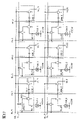
- FIG. 16 illustrates an example of a pixel circuit and a memory circuit provided over a plurality of lines.
- a pixel circuit 62_1R, a pixel circuit 62_1G, and a pixel circuit 62_1B are shown as pixel circuits that function as sub-pixels in the first row.
- the light emitting element 70R_1, the light emitting element 70G_1, and the light emitting element 70B_1 are shown.
- the memory circuit 82B_1 is shown as the memory circuit on the first line.
- a pixel circuit 62_2R, a pixel circuit 62_2G, and a pixel circuit 62_2B are shown as pixel circuits that function as sub-pixels in the second row.
- the memory circuit 82B_2 is shown as the memory circuit on the second line.
- the memory circuits 82B_1 and 82B_2 are connected to the nodes holding the data in the functional circuits 50_1 and 50_1.
- the functional circuits 50_1 and 50_1 correspond to different terminals in the functional circuit 50.
- FIG. 16 illustrates the wiring GL_1 that functions as the wiring GL of the first line and the wiring GL_1 that functions as the wiring GL of the second line.
- FIG. 16 illustrates wiring SL_R, SL_G, SL_B, wiring ANO, and wiring VCOM that function as source lines.
- FIG. 16 illustrates the wiring ML_1 for supplying the signal BKH for controlling the memory circuit 82B_1 and the wiring ML_2 for supplying the signal BKH for controlling the memory circuit 82B_1.
- the code may be a code for identifying a line number such as "_1" or “_2", “R”, or “R”.
- a code for identifying each color controlled by the sub-pixels such as "G” and "B” may be added and described.
- FIG. 8A including the switch SW21 and the transistor M21 is applied as the pixel circuits 62_1 and 62_2 shown in FIG. 16 is shown.
- the memory circuit 82B may be configured to be arranged between a set of pixel circuits (pixel circuits 62_1R, 62_1G, and 62_1B) that control RGB.
- connection of the back gate electrodes of the transistors of the pixel circuits 62_1 and 62_2 and the memory circuits 82B_1 and 82B_2 is omitted, but may be configured to be connected to each other.
- the back gate electrodes of the transistors of the pixel circuit 62 and the memory circuit 82B in the same row may be connected to each other.
- the back gate electrodes of the transistors of the pixel circuit 62 may be connected to each other, and the back gate electrodes of the transistors of the memory circuit 82B may be connected to each other separately. That is, it is preferable that the wiring for connecting the back gate electrode of the transistor of the pixel circuit 62 and the wiring for connecting the back gate electrode of the transistor of the memory circuit 82B are separate wiring.
- the memory circuit 82B provided together with the pixel circuit 62 can be provided corresponding to the RGB sub-pixels.
- the memory circuit 82B can hold the data of the circuit provided in the layer 20 such as the functional circuit 50 or the CPU 51 by using the OS transistor. Since the memory circuit 82B provided in the layer 30 in which the OS transistor is provided can be uniformly arranged in the layer 30, the memory circuit 82B and the functional circuit are different from the case where the memory circuit 82B is locally arranged. It becomes possible to easily make an electrical connection with the 50 or the CPU 51.
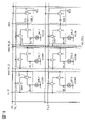
- FIG. 17 illustrates an example of a pixel circuit and a memory circuit provided over a plurality of lines, which have a configuration different from that of FIG.
- FIG. 16 shows a configuration in which a memory circuit 82B is provided corresponding to a set of pixel circuits 62_1 and 62_2 that control RGB, but in FIG. 17, a memory circuit 82B is arranged for each set of pixel circuits that control RGB.
- the configuration is illustrated.
- the functional circuits 50_11, 50_12, 50_13, 50_21, 50_22, and 50_23 correspond to different terminals in the functional circuit 50.
- more memory circuits 82B than the configuration of FIG. 16 can be provided on the layer 30 in which the OS transistor is provided.
- the memory circuit 82B and the functional circuit 50 do not depend on the circuit arrangement of the functional circuit 50 or the CPU 51. Alternatively, it becomes possible to easily make an electrical connection with the CPU 51.
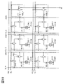
- FIG. 18 illustrates an example of a pixel circuit and a memory circuit provided over a plurality of lines, which have different configurations from those of FIGS. 16 and 17.
- the wiring ML_1 and the wiring ML_2 are configured as a common wiring ML.
- the wiring ML is wiring for supplying a signal BKH for controlling the memory circuit 82B_1 and the memory circuit 82B_2. Further, the wiring ML is configured to connect the wiring provided in different rows with the wiring provided in parallel with the wiring provided in the column direction.
- the wiring ML_COL provided in parallel with the wiring provided in the column direction can reduce the influence of noise between the pixel circuits by arranging the wiring ML_COL between the pixel circuits of the sub-pixels, for example.
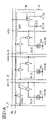
- FIG. 19 illustrates an example of a pixel circuit and a memory circuit provided over a plurality of lines having a configuration different from that of FIGS. 16 to 18.
- the memory circuit 82B_1 on the first line and the memory circuit 82B_1 on the second line are connected to the same node that holds the data in the functional circuit 50. Since the memory circuit 82B_1 and the memory circuit 82B_1 can control the transistor M11 at different timings by different signals, the configuration is such that the node data in the functional circuit 50 is acquired and held at a plurality of timings. Can be done.
- FIG. 20A shows a modification of the memory circuit 82B_1 in the first line and / or the memory circuit 82B_2 in the second line shown in FIGS. 16 to 19.
- FIG. 20A illustrates a configuration in which the terminal of the capacitance C11 on the side connected to the wiring ANO is connected to a node to which a fixed potential is given in the functional circuit 50 on the layer 20 side.
- the terminal of the capacitance C11 on the side connected to the wiring ANO is connected to the node to which the fixed potential is given in the functional circuit 50 on the layer 20 side, and is connected to the gate electrode of the transistor M11.
- the wiring ML to be performed is omitted, and the configuration in which a signal for control is given from the functional circuit 50 on the layer 20 side is illustrated.
- the functional circuits 50_1A, 50_1B, and 50_1C represent different terminals in the functional circuit 50. With this configuration, the configuration of the memory circuit 82B in the layer 30 can be reduced, and the area occupied by the pixel circuit 62 can be increased.
- FIG. 21A shows a modification of the memory circuit 82B as in FIGS. 20A and 20B.
- FIG. 21A illustrates a configuration in which the capacitance C11 in the memory circuit 82B is provided in the functional circuit 50 on the layer 20 side.
- the capacitance C11 in the memory circuit 82B is provided in the functional circuit 50 on the layer 20 side, and the wiring ML connected to the gate electrode of the transistor M11 is omitted, and the functional circuit on the layer 20 side is omitted.
- the configuration which gives the signal to control from 50 is illustrated. With this configuration, the configuration of the memory circuit 82B in the layer 30 can be reduced, and the area occupied by the pixel circuit 62 can be increased.
- FIG. 22A shows a modified example in which the backup circuit 82 described in FIG. 14B is applied instead of the memory circuit 82B described in FIGS. 16 to 20.
- FIG. 22A illustrates a configuration in which the terminal of the capacitance C11 in the backup circuit 82 is connected to the wiring ANO.
- FIG. 22B illustrates a configuration in which the terminal of the capacitance C11 in the backup circuit 82 is connected to the transistor M12.
- the scan flip-flops 81_A, 81_B, and 81_C represent different terminals in the scan flip-flop 81. With this configuration, it is also possible to hold the data of the node in the functional circuit 50 in the capacitance C11.
- FIG. 23A shows a modified example of the backup circuit 82, similarly to FIGS. 22A and 22B.
- FIG. 23A illustrates a configuration in which the capacitance C11 in the backup circuit 82 is provided on the layer 20 side of the scan flip-flop 81.
- the capacitance C11 in the backup circuit 82 is provided on the layer 20 side of the scan flip-flop 81, and is connected to the wiring connected to the gate electrode of the transistor M11 and the gate of the transistor M12.
- the wiring is omitted, and the configuration in which signals BUH and RH for control from the functional circuit 50 on the layer 20 side are given is illustrated.
- the configuration of the backup circuit 82 in the layer 30 can be reduced, and the area occupied by the pixel circuit 62 can be increased.
- the connection of the back gate electrodes of the transistors of the pixel circuit 62 and the backup circuit 82 is omitted in FIGS. 22A to 23B, they may be connected to each other.
- the back gate electrodes of the transistors of the pixel circuit 62 and the backup circuit 82 in the same row may be connected to each other.
- the back gate electrodes of the transistors of the pixel circuit 62 may be connected to each other, and the back gate electrodes of the transistors of the backup circuit 82 may be connected to each other separately. That is, it is preferable that the wiring for connecting the back gate electrode of the transistor of the pixel circuit 62 and the wiring for connecting the back gate electrode of the transistor of the backup circuit 82 are separate wiring.
- FIG. 24A shows an example of a circuit configuration different from the above-mentioned memory circuit 82B and backup circuit 82 provided in the layer 30.
- the arithmetic circuit 82C shown in FIG. 24A is an example of a circuit that performs a product-sum operation and an activation function operation.
- the arithmetic circuit 82C shown in FIG. 24A is a circuit that performs a product-sum operation of the first data and the second data. Since the calculation circuit 82C performs the product-sum calculation using a plurality of data, it is preferable to provide a plurality of calculation circuits 82C.
- the arithmetic circuit 82C has a transistor M31, a transistor M32, and a capacitance CP.
- the transistor M31 is preferably an OS transistor.
- OS transistor By using an OS transistor as the transistor M31, the leakage current of the transistor M31 can be suppressed. Therefore, the data required for the calculation can be held in the node NM as an electric charge for a long time, and a product-sum calculation circuit with high calculation accuracy can be realized. Since the refreshing operation of the potential of the node NM can be reduced, the power consumption of the product-sum calculation circuit can be reduced.
- the OS transistor for the transistor M32, it can be manufactured at the same time as the transistor M31, so that the manufacturing process of the product-sum calculation circuit can be shortened.
- the first terminal of the transistor M31 is electrically connected to the gate of the transistor M32.
- the first terminal of the transistor M32 is electrically connected to the wiring VR .
- the first terminal of the capacitance CP is electrically connected to the gate of the transistor M32.
- the second terminal of the transistor M31 is electrically connected to the wiring BW, and the gate of the transistor M31 is electrically connected to the wiring WW.
- the second terminal of the transistor M32 is electrically connected to the wiring V Y , and the second terminal of the capacitance CP is electrically connected to the wiring V X.
- the current flowing from the wiring V Y to the second terminal of the transistor M32 is defined as IAM.
- the electric charge corresponding to the data is held in the node NM, and the potential of the wiring VX is changed to change the potential of the gate of the transistor M32 which is electrically suspended, and the transistor M32 is changed. It is possible to obtain the multiplication result for the flowing current I AM . Then, by adding the currents I AM flowing through the plurality of arithmetic circuits 82C, the product-sum operation corresponding to the sum of the multiplication results can be executed.
- FIG. 24B shows a modified example in which the arithmetic circuit 82C described in FIG. 24A is applied instead of the memory circuit 82B or the backup circuit 82 described in FIGS. 16 to 23.
- FIG. 25A illustrates a configuration in which the capacitance CP in the arithmetic circuit 82C is provided on the layer 30 side.
- the OS transistor provided in the layer 30 may have a configuration in which the transistor characteristics are different for each transistor.
- the transistor M31 is required to suppress the leak current in order to retain the electric charge
- the transistor M32 is preferably a transistor provided with a semiconductor layer having high mobility for passing the current IAM .
- FIG. 25B provides the capacitance CP in the arithmetic circuit 82C on the layer 20 side, omits the wiring connected to the gate electrode of the transistor M31 and the wiring connected to the transistor M32, and omits the wiring on the layer 20 side.
- the wiring BW and WWL for controlling from the functional circuit 50, and the terminals for providing the wirings VR , V Y , and V X are shown in the figure.
- the transistor M31 is shown as an OS transistor provided on the layer 30, and the transistor M32 is shown as a Si transistor provided on the layer 20.
- connection of the back gate electrodes of the transistors of the pixel circuit 62 and the arithmetic circuit 82C may be connected to each other.
- the back gate electrodes of the transistors of the pixel circuit 62 and the arithmetic circuit 82C in the same row may be connected to each other.
- the back gate electrodes of the transistors of the pixel circuit 62 may be connected to each other, and the back gate electrodes of the transistors of the arithmetic circuit 82C may be connected to each other separately. That is, it is preferable that the wiring for connecting the back gate electrode of the transistor of the pixel circuit 62 and the wiring for connecting the back gate electrode of the transistor of the arithmetic circuit 82C are separate wiring.
- FIG. 26A shows an example of a circuit configuration different from the above-mentioned memory circuit 82B and backup circuit 82 provided in the layer 30.
- the block circuit 82D shown in FIG. 26A represents a sequential circuit or a combinational circuit such as a flip-flop, an inverter, and a shift register. It is preferable that a plurality of block circuits 82D are provided in combination.
- the block circuit 82D is provided between the wirings that provide the power supply potential (VDD-VSS). Further, the block circuit 82D is connected to the transistor M41 as shown in FIG. 26A.
- the transistor M41 is preferably an OS transistor.
- the transistor M41 can be provided with a period for turning off the transistor M41 by the control signal PSW. By turning off the transistor M41, the potential of the node V VDD can be made smaller than the VDD, so that the leakage current flowing between the wirings that give the power supply potential (VDD-VSS) via the block circuit 82D can be suppressed. .. Therefore, power consumption can be reduced by turning off the transistor M41 during the period when the block circuit 82D does not operate.
- FIG. 26B shows a modified example in which the block circuit 82D described in FIG. 26A is applied instead of the memory circuit 82B or the backup circuit 82 described in FIGS. 16 to 23.
- FIG. 26A illustrates a configuration in which the block circuit 82D is provided on the layer 20 side and the transistor M41 is provided on the layer 30 side. With this configuration, the transistor M41 can be arranged so as to overlap the block circuit 82D, so that the power consumption can be reduced without increasing the area occupied by the block circuit 82D.
- the transistor of the gate driver 41 included in the drive circuit 40 is used as an OS transistor, and the gate driver 41 (shown as a gate driver 41L and a gate driver 41R on both sides of the display unit 60 in the figure) is used as a layer 30.
- the gate driver 41 shown as a gate driver 41L and a gate driver 41R on both sides of the display unit 60 in the figure.
- FIG. 27B is an example of a configuration in which a part of the function of the source driver 42 of the drive circuit 40 is provided in the layer 30 in FIG. 27A.
- FIG. 27B is an example of a configuration in which the transistor of the demultiplexer that distributes the signal output by the source driver 42 to each source line is an OS transistor and is provided on the layer 30 as the demultiplexer 42DEM. With this configuration, the number of wirings from the drive circuit 40 in the layer 20 to the display unit 60 in the layer 30 can be further reduced.
- FIG. 28 is a cross-sectional view showing a configuration example of the display device 10.
- the display device 10 has a substrate 701 and a substrate 705, and the substrate 701 and the substrate 705 are bonded to each other by a sealing material 712.
- a single crystal semiconductor substrate such as a single crystal silicon substrate can be used.
- a semiconductor substrate other than the single crystal semiconductor substrate may be used as the substrate 701.
- a transistor 441 and a transistor 601 are provided on the substrate 701.
- the transistor 441 and the transistor 601 can be a transistor provided on the layer 20 shown in the first embodiment.
- the transistor 441 is composed of a conductor 443 having a function as a gate electrode, an insulator 445 having a function as a gate insulator, and a part of a substrate 701, and is a semiconductor region 447 including a channel forming region and a source region. Alternatively, it has a low resistance region 449a having a function as one of the drain regions and a low resistance region 449b having a function as the other of the source region or the drain region.
- the transistor 441 may be either a p-channel type or an n-channel type.
- the transistor 441 is electrically separated from other transistors by the element separation layer 403.
- FIG. 28 shows a case where the transistor 441 and the transistor 601 are electrically separated by the element separation layer 403.
- the element separation layer 403 can be formed by using a LOCOS (LOCOExidation of Silicon) method, an STI (Shallow Trench Isolation) method, or the like.
- the semiconductor region 447 has a convex shape. Further, the side surface and the upper surface of the semiconductor region 447 are provided so as to be covered by the conductor 443 via the insulator 445. Note that FIG. 28 does not show how the conductor 443 covers the side surface of the semiconductor region 447. Further, a material for adjusting the work function can be used for the conductor 443.
- a transistor having a convex shape in the semiconductor region can be called a fin type transistor because the convex portion of the semiconductor substrate is used.
- it may have an insulator which is in contact with the upper part of the convex portion and has a function as a mask for forming the convex portion.
- FIG. 28 shows a configuration in which a part of the substrate 701 is processed to form a convex portion, the SOI substrate may be processed to form a semiconductor having a convex shape.
- the configuration of the transistor 441 shown in FIG. 28 is an example, and is not limited to the configuration, and may be an appropriate configuration according to the circuit configuration, the circuit operation method, and the like.
- the transistor 441 may be a planar transistor.
- the transistor 601 can have the same configuration as the transistor 441.
- an insulator 405, an insulator 407, an insulator 409, and an insulator 411 are provided.
- the conductor 451 is embedded in the insulator 405, the insulator 407, the insulator 409, and the insulator 411.
- the height of the upper surface of the conductor 451 and the height of the upper surface of the insulator 411 can be made the same.
- the insulator 421 and the insulator 214 are provided on the conductor 451 and the insulator 411.
- the conductor 453 is embedded in the insulator 421 and in the insulator 214.
- the height of the upper surface of the conductor 453 and the height of the upper surface of the insulator 214 can be made equal to each other.
- the insulator 216 is provided on the conductor 453 and the insulator 214.
- a conductor 455 is embedded in the insulator 216.
- the height of the upper surface of the conductor 455 and the height of the upper surface of the insulator 216 can be made equal to each other.
- Insulator 222, insulator 224, insulator 254, insulator 280, insulator 274, and insulator 281 are provided on the conductor 455 and the insulator 216.
- the conductor 305 is embedded in the insulator 222, the insulator 224, the insulator 254, the insulator 280, the insulator 274, and the insulator 281.
- the height of the upper surface of the conductor 305 and the height of the upper surface of the insulator 281 can be made equal to each other.
- the insulator 361 is provided on the conductor 305 and the insulator 281.
- a conductor 317 and a conductor 337 are embedded in the insulator 361.
- the height of the upper surface of the conductor 337 and the height of the upper surface of the insulator 361 can be made the same.
- the insulator 363 is provided on the conductor 337 and the insulator 361.
- a conductor 347, a conductor 353, a conductor 355, and a conductor 357 are embedded in the insulator 363.
- the height of the upper surface of the conductor 353, the conductor 355, and the conductor 357 can be made the same as the height of the upper surface of the insulator 363.
- connection electrode 760 is provided on the conductor 353, the conductor 355, the conductor 357, and the insulator 363. Further, an anisotropic conductor 780 is provided so as to be electrically connected to the connection electrode 760, and an FPC (Flexible Printed Circuit) 716 is provided so as to be electrically connected to the anisotropic conductor 780. Various signals and the like are supplied to the display device 10 from the outside of the display device 10 by the FPC 716.
- FPC Flexible Printed Circuit
- the low resistance region 449b having a function as the other of the source region or the drain region of the transistor 441 includes a conductor 451 and a conductor 453, a conductor 455, a conductor 305, a conductor 317, and a conductor. It is electrically connected to the FPC 716 via a 337, a conductor 347, a conductor 353, a conductor 355, a conductor 357, a connection electrode 760, and an anisotropic conductor 780.
- FIG. 28 the low resistance region 449b having a function as the other of the source region or the drain region of the transistor 441 includes a conductor 451 and a conductor 453, a conductor 455, a conductor 305, a conductor 317, and a conductor. It is electrically connected to the FPC 716 via a 337, a conductor 347, a conductor 353, a conductor 355, a conductor 357, a connection electrode 760, and an anis
- connection electrode 760 and the conductor 347 shows three conductors having a function of electrically connecting the connection electrode 760 and the conductor 347, that is, the conductor 353, the conductor 355, and the conductor 357, which is one of the present inventions.
- the embodiment is not limited to this.
- the number of conductors having a function of electrically connecting the connection electrode 760 and the conductor 347 may be one, two, or four or more.
- the contact resistance can be reduced by providing a plurality of conductors having a function of electrically connecting the connection electrode 760 and the conductor 347.
- a transistor 750 is provided on the insulator 214.
- the transistor 750 can be a transistor provided on the layer 30 shown in the first embodiment.
- it may be a transistor provided in the pixel circuit 62.
- an OS transistor can be preferably used as the transistor 750.
- the OS transistor has a feature that the off-current is extremely small. Therefore, since the holding time of the image data or the like can be lengthened, the frequency of the refreshing operation can be reduced. Therefore, the power consumption of the display device 10 can be reduced.
- the transistor 750 can be a transistor provided in the backup circuit 82.
- an OS transistor can be preferably used.
- the OS transistor has a feature that the off-current is extremely small. Therefore, the data contained in the flip-flop can be retained even during the period when the sharing of the power supply voltage is stopped. Therefore, it is possible to perform a normally-off operation of the CPU (an operation of intermittently stopping the power supply voltage). Therefore, the power consumption of the display device 10 can be reduced.
- Conductors 301a and 301b are embedded in the insulator 254, the insulator 280, the insulator 274, and the insulator 281.
- the conductor 301a is electrically connected to one of the source or drain of the transistor 750
- the conductor 301b is electrically connected to the other of the source or drain of the transistor 750.
- the height of the upper surface of the conductor 301a and the conductor 301b can be made the same as the height of the upper surface of the insulator 281.
- Conductor 311 and conductor 313, conductor 331, capacity 790, conductor 333, and conductor 335 are embedded in the insulator 361.
- the conductor 311 and the conductor 313 are electrically connected to the transistor 750 and have a function as wiring.
- the conductor 333 and the conductor 335 are electrically connected to the capacity 790.
- the height of the upper surface of the conductor 331, the conductor 333, and the conductor 335 can be made the same as the height of the upper surface of the insulator 361.
- Conductor 341, conductor 343, and conductor 351 are embedded in the insulator 363.
- the height of the upper surface of the conductor 351 and the height of the upper surface of the insulator 363 can be made the same.
- the insulator 405, the insulator 407, the insulator 409, the insulator 411, the insulator 421, the insulator 214, the insulator 280, the insulator 274, the insulator 281 and the insulator 361, and the insulator 363 are used as an interlayer film. It may have a function and may have a function as a flattening film that covers each lower uneven shape. For example, the upper surface of the insulator 363 may be flattened by a flattening treatment using a chemical mechanical polishing (CMP) method or the like in order to improve the flatness.
- CMP chemical mechanical polishing
- the capacitance 790 has a lower electrode 321 and an upper electrode 325. Further, an insulator 323 is provided between the lower electrode 321 and the upper electrode 325. That is, the capacitance 790 is a laminated structure in which an insulator 323 that functions as a dielectric is sandwiched between a pair of electrodes.
- FIG. 28 shows an example in which the capacity 790 is provided on the insulator 281, the capacity 790 may be provided on an insulator different from the insulator 281.
- FIG. 28 shows an example in which the conductor 301a, the conductor 301b, and the conductor 305 are formed in the same layer. Further, an example is shown in which the conductor 311 and the conductor 313, the conductor 317, and the lower electrode 321 are formed in the same layer. Further, an example is shown in which the conductor 331, the conductor 333, the conductor 335, and the conductor 337 are formed in the same layer. Further, an example is shown in which the conductor 341, the conductor 343, and the conductor 347 are formed in the same layer. Further, an example is shown in which the conductor 351 and the conductor 353, the conductor 355, and the conductor 357 are formed in the same layer.
- the display device 10 shown in FIG. 28 has a light emitting element 70.
- the light emitting element 70 has a conductor 772, an EL layer 786, and a conductor 788.
- the EL layer 786 has an organic compound or an inorganic compound such as a quantum dot.
- Examples of materials that can be used for organic compounds include fluorescent materials and phosphorescent materials.
- Examples of materials that can be used for quantum dots include colloidal quantum dot materials, alloy-type quantum dot materials, core-shell type quantum dot materials, and core-type quantum dot materials.
- the conductor 772 is electrically connected to the other of the source or drain of the transistor 750 via the conductor 351 and the conductor 341, the conductor 331, the conductor 313, and the conductor 301b.
- the conductor 772 is formed on the insulator 363 and has a function as a pixel electrode.
- a material that is transparent to visible light or a material that is reflective can be used.
- the translucent material for example, an oxide material containing indium, zinc, tin and the like may be used.
- the reflective material for example, a material containing aluminum, silver, etc. may be used.
- the display device 10 can be provided with an optical member (optical substrate) such as a polarizing member, a retardation member, and an antireflection member.
- an optical member optical substrate
- polarizing member such as a polarizing member, a retardation member, and an antireflection member.
- a light-shielding layer 738 and an insulator 734 in contact with the light-shielding layer 738 are provided on the substrate 705 side.
- the light-shielding layer 738 has a function of blocking light emitted from an adjacent region.
- the light-shielding layer 738 has a function of blocking external light from reaching the transistor 750 or the like.
- an insulator 730 is provided on the insulator 363.
- the insulator 730 can be configured to cover a part of the conductor 772.
- the light emitting element 70 has a translucent conductor 788, and can be a top emission type light emitting element.
- the light emitting element 70 may have a bottom emission structure that emits light to the conductor 772 side, or a dual emission structure that emits light to both the conductor 772 and the conductor 788.
- the light-shielding layer 738 is provided so as to have a region overlapping with the insulator 730. Further, the light-shielding layer 738 is covered with an insulator 734. Further, the space between the light emitting element 70 and the insulator 734 is filled with a sealing layer 732.
- the structure 778 is provided between the insulator 730 and the EL layer 786. Further, the structure 778 is provided between the insulator 730 and the insulator 734.
- FIG. 29 shows the Si transistor of the drive circuit 40 included in the layer 20, the OS transistor (regions 40, 62) included in the pixel circuit 62 included in the layer 30, and the functional circuit 50 included in the layer 20 described in the first embodiment. It is sectional drawing in the case of the Si transistor of the above, and the OS transistor (regions 50, 82) included in the backup circuit 82 included in the layer 30. The description of the cross-sectional view shown in FIG. 29 is the same as each configuration of the cross-sectional view shown in FIG. 28.
- the layer 20 may be provided with the Si transistor 91 of the drive circuit 40 and the Si transistor 94 of the functional circuit 50.
- the layer 30 may be provided with the OS transistor 92 and the capacity 93 of the pixel circuit 62, and the OS transistor 95 and the capacity 96 of the backup circuit 82.
- a light emitting element 70 can be provided on the upper layer of the layer 30.
- FIG. 30A is a diagram schematically showing a state of data backup in the functional circuit 50 provided in the layer 20 in the configuration example of the display device 10 described in the first embodiment.
- FIG. 30A illustrates a configuration example in which the backup circuit 82 is provided in each pixel 61 in the display unit 60 provided in the layer 30.
- the backup circuit 82 shown in FIG. 30A is uniformly arranged on the display unit 60
- the backup circuit 82 is arranged close to the flip-flop 80 for transmitting and receiving the backup data BD.
- the backup data can be transmitted / received to / from the backup circuit 82 directly above the flip-flop 80 regardless of the location of the layer 20. ..
- backup data is transmitted and received to and from the circuit (for example, flip-flop 80) of the functional circuit 50 directly underneath, and in the backup circuit 82F of FIG. 30A, the circuit and backup of the functional circuit 50 directly underneath are backed up. It can be configured so that data is not transmitted or received.
- FIG. 30B shows a schematic cross-sectional view corresponding to the configuration described with reference to FIG. 30A.
- the layer 20 is provided with a wiring 97 for making an electrical connection between the layer 20 and the layer 30.
- a transistor 94M can be electrically connected to a transistor 95M and a capacity 96M on the layer 30.
- no wiring 97 for making an electrical connection between the layer 20 and the layer 30 is provided between the circuit of the functional circuit 50 and the backup circuit 82F for transmitting and receiving backup data.
- the transistor 94M in the layer 20 and the transistor 95M and the capacity 96M in the layer 30 are not electrically connected.
- the backup circuit 82F which is not electrically connected to the circuit of the functional circuit 50, may have each terminal electrically suspended or may be connected to a wiring to which a fixed potential is given.
- data is calculated by having a configuration in which the electrical connection between the circuit of the functional circuit 50 in the layer 20 and the backup circuit 82 in the layer 30 can be selected. Even if the arrangement of the functional circuit 50 to be processed is changed in the layer 20, it is possible to secure the connection with the backup circuit that backs up the data only by changing the layout of the wiring layer.
- FIG. 31 A modified example of the display device 10 shown in FIG. 28 is shown in FIG. 31.
- the display device 10 shown in FIG. 31 differs from the display device 10 shown in FIG. 28 in that the colored layer 736 is provided.
- the colored layer 736 is provided so as to have a region overlapping with the light emitting element 70.
- the color purity of the light extracted from the light emitting element 70 can be increased.
- a high-quality image can be displayed on the display device 10.
- all the light emitting elements 70 of the display device 10 can be light emitting elements that emit white light, it is not necessary to form the EL layer 786 by painting separately, and the display device 10 has a high definition. can do.
- the light emitting element 70 can have a micro-optical resonator (microcavity) structure.
- a predetermined color for example, RGB
- the display device 10 can perform color display.
- the display device 10 can display a high-brightness image, and the power consumption of the display device 10 can be reduced.
- the EL layer 786 is formed in an island shape for each pixel or in a striped shape for each pixel row, that is, when the EL layer 786 is formed by painting separately, it is possible to form a configuration in which the colored layer is not provided.
- the brightness of the display device 10 can be, for example, 500 cd / m 2 or more, preferably 1000 cd / m 2 or more and 10000 cd / m 2 or less, and more preferably 2000 cd / m 2 or more and 5000 cd / m 2 or less.
- FIG. 32 A modification of FIG. 31 is shown in FIG. 32.
- the display device 10 shown in FIG. 32 is mainly different from the display device 10 shown in FIG. 31 in that the display device 10 has the transistor 602 and the transistor 603 which are OS transistors instead of the transistor 441 and the transistor 601. Further, as the transistor 750, an OS transistor can be used. That is, the display device 10 shown in FIG. 32 is provided with OS transistors stacked.
- An insulator 613 and an insulator 614 are provided on the substrate 701, and a transistor 602 and a transistor 603 are provided on the insulator 614.
- a transistor or the like may be provided between the substrate 701 and the insulator 613.
- a transistor having the same configuration as the transistor 441 and the transistor 601 shown in FIG. 31 may be provided between the substrate 701 and the insulator 613.
- the transistor 602 and the transistor 603 can be a transistor provided on the layer 20 shown in the first embodiment.
- the transistor 602 and the transistor 603 can be a transistor having the same configuration as the transistor 750.
- the transistor 602 and the transistor 603 may be an OS transistor having a configuration different from that of the transistor 750.
- an insulator 616, an insulator 622, an insulator 624, an insulator 654, an insulator 680, an insulator 674, and an insulator 681 are provided on the insulator 614.
- the conductor 461 is embedded in the insulator 654, the insulator 680, the insulator 674, and the insulator 681.
- the height of the upper surface of the conductor 461 and the height of the upper surface of the insulator 681 can be made the same.
- the insulator 501 is provided on the conductor 461 and the insulator 681.
- a conductor 463 is embedded in the insulator 501.
- the height of the upper surface of the conductor 463 and the height of the upper surface of the insulator 501 can be made the same.
- the insulator 421 and the insulator 214 are provided on the conductor 463 and the insulator 501.
- the conductor 453 is embedded in the insulator 421 and in the insulator 214.
- the height of the upper surface of the conductor 453 and the height of the upper surface of the insulator 214 can be made equal to each other.
- one of the source and drain of the transistor 602 is a conductor 461, a conductor 463, a conductor 453, a conductor 455, a conductor 305, a conductor 317, a conductor 337, a conductor 347, and a conductor. It is electrically connected to the FPC 716 via a body 353, a conductor 355, a conductor 357, a connection electrode 760, and an anisotropic conductor 780.
- the insulator 613, the insulator 614, the insulator 680, the insulator 674, the insulator 681, and the insulator 501 have a function as an interlayer film and a function as a flattening film covering the uneven shape below each. May have.
- the display device 10 By configuring the display device 10 as shown in FIG. 32, all the transistors of the display device 10 can be used as OS transistors while the display device 10 is narrowed and downsized. Thereby, for example, the transistor provided in the layer 20 shown in the first embodiment and the transistor provided in the layer 30 can be manufactured by using the same device. Therefore, the manufacturing cost of the display device 10 can be reduced, and the display device 10 can be made inexpensive.
- FIG. 33 is a cross-sectional view showing a configuration example of the display device 10. It is mainly different from the display device 10 shown in FIG. 31 in that a layer having a transistor 800 is provided between a layer having a transistor 750 and a layer having a transistor 601 and a transistor 441.
- the layer 20 shown in the first embodiment can be composed of a layer having a transistor 601 and a transistor 441 and a layer having a transistor 800.
- the transistor 750 can be a transistor provided on the layer 30 shown in the first embodiment.
- Insulator 821 and insulator 814 are provided on the conductor 451 and the insulator 411.
- the conductor 853 is embedded in the insulator 821 and in the insulator 814.
- the height of the upper surface of the conductor 853 and the height of the upper surface of the insulator 814 can be made the same.
- the insulator 816 is provided on the conductor 853 and the insulator 814.
- a conductor 855 is embedded in the insulator 816.
- the height of the upper surface of the conductor 855 and the height of the upper surface of the insulator 816 can be made about the same.
- Insulator 822, insulator 824, insulator 854, insulator 880, insulator 874, and insulator 881 are provided on the conductor 855 and the insulator 816.
- the conductor 805 is embedded in the insulator 822, the insulator 824, the insulator 854, the insulator 880, the insulator 874, and the insulator 881.
- the height of the upper surface of the conductor 805 and the height of the upper surface of the insulator 881 can be made the same.
- Insulator 421 and insulator 214 are provided on the conductor 817 and the insulator 881.
- the low resistance region 449b having a function as the other of the source region or the drain region of the transistor 441 includes a conductor 451 and a conductor 853, a conductor 855, a conductor 805, a conductor 817, and a conductor.
- a transistor 800 is provided on the insulator 814.
- the transistor 800 can be a transistor provided on the layer 20 shown in the first embodiment.
- the transistor 800 is preferably an OS transistor.
- the transistor 800 can be a transistor provided in the backup circuit 82.
- Conductors 801a and 801b are embedded in the insulator 854, the insulator 880, the insulator 874, and the insulator 881.
- the conductor 801a is electrically connected to one of the source or drain of the transistor 800
- the conductor 801b is electrically connected to the other of the source or drain of the transistor 800.
- the height of the upper surface of the conductor 801a and the conductor 801b can be made the same as the height of the upper surface of the insulator 881.
- the transistor 750 can be a transistor provided on the layer 30 shown in the first embodiment.
- the transistor 750 can be a transistor provided in the pixel circuit 62.
- the transistor 750 is preferably an OS transistor.
- the 274, the insulator 281 and the insulator 361, and the insulator 363 have a function as an interlayer film, and may have a function as a flattening film that covers the uneven shape below each of them.
- FIG. 33 shows an example in which the conductor 801a, the conductor 801b, and the conductor 805 are formed in the same layer. Further, an example is shown in which the conductor 811, the conductor 813, and the conductor 817 are formed in the same layer.
- FIG. 34 is a cross-sectional view showing a configuration example of the display device 10. It is mainly different from the display device 10 shown in FIG. 31 in that the layer having the transistor 750 is omitted in the illustration.
- the Si transistor in the layer 20 shown in the first embodiment for example, the transistor 601 can be used as the transistor corresponding to the transistor 750 which is the OS transistor. Since the transistor 601 is used as a transistor having a small off current, a configuration in which the channel length is longer than that of the transistor 441 is preferable.
- the layer in which the conductor functions as wiring is also omitted.
- a plurality of layers in which the conductor functions as wiring may be provided between the layer having the Si transistor of the transistor 601 and the transistor 441 and the layer having the light emitting element 70.
- This embodiment can be carried out by appropriately combining at least a part thereof with other embodiments described in the present specification.
- 35A, 35B, and 35C are a top view and a cross-sectional view of the transistor 200A, which can be used in the display device according to one aspect of the present invention, and the periphery of the transistor 200A.
- a transistor 200A can be applied to the display device of one aspect of the present invention.
- FIG. 35A is a top view of the transistor 200A.
- 35B and 35C are cross-sectional views of the transistor 200A.
- FIG. 35B is a cross-sectional view of the portion shown by the alternate long and short dash line of A1-A2 in FIG. 35A, and is also a cross-sectional view of the transistor 200A in the channel length direction.
- FIG. 35C is a cross-sectional view of the portion shown by the alternate long and short dash line of A3-A4 in FIG. 35A, and is also a cross-sectional view of the transistor 200A in the channel width direction.
- some elements are omitted for the sake of clarity of the figure.
- the transistor 200A is composed of a metal oxide 230a arranged on a substrate (not shown), a metal oxide 230b arranged on the metal oxide 230a, and a metal oxide 230b.
- Insulator 280 arranged above the conductors 242a and 242b spaced apart from each other and on the conductors 242a and 242b with an opening formed between the conductors 242a and the conductors 242b.
- the conductor 260 arranged in the opening, the metal oxide 230b, the conductor 242a, the conductor 242b, and the insulator 280, the insulator 250 arranged between the conductor 260, and the metal.
- the conductor 242a and the conductor 242b may be collectively referred to as a conductor 242.
- the side surfaces of the conductor 242a and the conductor 242b on the conductor 260 side have a substantially vertical shape.
- the transistor 200A shown in FIG. 35 is not limited to this, and the angle formed by the side surface and the bottom surface of the conductor 242a and the conductor 242b is 10 ° or more and 80 ° or less, preferably 30 ° or more and 60 ° or less. May be. Further, the opposing side surfaces of the conductor 242a and the conductor 242b may have a plurality of surfaces.
- the insulator 254 is arranged between the insulator 224, the metal oxide 230a, the metal oxide 230b, the conductor 242a, the conductor 242b, the metal oxide 230c, and the insulator 280. Is preferable.
- the insulator 254 includes a side surface of the metal oxide 230c, an upper surface and a side surface of the conductor 242a, an upper surface and a side surface of the conductor 242b, and the metal oxide 230a and the metal oxide 230b. It is preferable to be in contact with the side surface of the insulator and the upper surface of the insulator 224.
- the transistor 200A has a configuration in which three layers of a metal oxide 230a, a metal oxide 230b, and a metal oxide 230c are laminated in a region where a channel is formed (hereinafter, also referred to as a channel formation region) and in the vicinity thereof.
- a two-layer structure of the metal oxide 230b and the metal oxide 230c, or a laminated structure of four or more layers may be provided.
- the conductor 260 is shown as a two-layer laminated structure, but the present invention is not limited to this.
- the conductor 260 may have a single-layer structure or a laminated structure of three or more layers.
- each of the metal oxide 230a, the metal oxide 230b, and the metal oxide 230c may have a laminated structure of two or more layers.
- the metal oxide 230c has a laminated structure consisting of a first metal oxide and a second metal oxide on the first metal oxide
- the first metal oxide is the metal oxide 230b. It has a similar composition
- the second metal oxide preferably has the same composition as the metal oxide 230a.
- the conductor 260 functions as a gate electrode of the transistor, and the conductor 242a and the conductor 242b function as a source electrode or a drain electrode, respectively.
- the conductor 260 is formed so as to be embedded in the opening of the insulator 280 and the region sandwiched between the conductor 242a and the conductor 242b.
- the arrangement of the conductor 260, the conductor 242a, and the conductor 242b is selected in a self-aligned manner with respect to the opening of the insulator 280. That is, in the transistor 200A, the gate electrode can be arranged in a self-aligned manner between the source electrode and the drain electrode. Therefore, since the conductor 260 can be formed without providing the alignment margin, the occupied area of the transistor 200A can be reduced. As a result, the display device can be made high-definition. Further, the display device can be made into a narrow frame.
- the conductor 260 preferably has a conductor 260a provided inside the insulator 250 and a conductor 260b provided so as to be embedded inside the conductor 260a.
- the transistor 200A includes an insulator 214 arranged on a substrate (not shown), an insulator 216 arranged on the insulator 214, and a conductor 205 arranged so as to be embedded in the insulator 216. It is preferable to have an insulator 222 arranged on the insulator 216 and the conductor 205, and an insulator 224 arranged on the insulator 222. It is preferable that the metal oxide 230a is arranged on the insulator 224.
- the insulator 274 that functions as an interlayer film and the insulator 281 are arranged on the transistor 200A.
- the insulator 274 is arranged in contact with the upper surface of the conductor 260, the insulator 250, the insulator 254, the metal oxide 230c, and the insulator 280.
- the insulator 222, the insulator 254, and the insulator 274 have a function of suppressing the diffusion of at least one hydrogen (for example, a hydrogen atom, a hydrogen molecule, etc.).
- the insulator 222, the insulator 254, and the insulator 274 preferably have lower hydrogen permeability than the insulator 224, the insulator 250, and the insulator 280.
- the insulator 222 and the insulator 254 have a function of suppressing the diffusion of oxygen (for example, at least one oxygen atom, oxygen molecule, etc.).
- the insulator 222 and the insulator 254 preferably have lower oxygen permeability than the insulator 224, the insulator 250, and the insulator 280.
- the insulator 224, the metal oxide 230, and the insulator 250 are separated from the insulator 280 and the insulator 281 by the insulator 254 and the insulator 274. Therefore, in the insulator 224, the metal oxide 230, and the insulator 250, impurities such as hydrogen contained in the insulator 280 and the insulator 281 or excess oxygen are added to the insulator 224, the metal oxide 230a, and the metal oxide. It is possible to suppress contamination with 230b and the insulator 250.
- a conductor 240 (conductor 240a and conductor 240b) that is electrically connected to the transistor 200A and functions as a plug is provided.
- An insulator 241 (insulator 241a and insulator 241b) is provided in contact with the side surface of the conductor 240 that functions as a plug. That is, the insulator 241 is provided in contact with the inner wall of the opening of the insulator 254, the insulator 280, the insulator 274, and the insulator 281. Further, the first conductor of the conductor 240 may be provided in contact with the side surface of the insulator 241 and the second conductor of the conductor 240 may be further provided inside.
- the height of the upper surface of the conductor 240 and the height of the upper surface of the insulator 281 can be made equal to each other.
- the transistor 200A shows a configuration in which the first conductor of the conductor 240 and the second conductor of the conductor 240 are laminated, but the present invention is not limited to this.
- the conductor 240 may be provided as a single layer or a laminated structure having three or more layers. When the structure has a laminated structure, an ordinal number may be given in the order of formation to distinguish them.
- the transistor 200A is a metal oxide 230 (metal oxide 230a, metal oxide 230b, and metal oxide 230c) containing a channel forming region, and a metal oxide (hereinafter, also referred to as an oxide semiconductor) that functions as an oxide semiconductor. ) Is preferably used.
- a metal oxide serving as the channel forming region of the metal oxide 230, it is preferable to use a metal oxide having a band gap of 2 eV or more, preferably 2.5 eV or more.
- the metal oxide preferably contains at least indium (In) or zinc (Zn). In particular, it is preferable to contain indium (In) and zinc (Zn). Further, in addition to these, it is preferable that the element M is contained.
- Elements M include aluminum (Al), gallium (Ga), yttrium (Y), tin (Sn), boron (B), titanium (Ti), iron (Fe), nickel (Ni), germanium (Ge), and zirconium.
- Zr molybdenum
- Mo lanthanum
- La cerium
- Ce neodymium
- Hf hafnium
- tungsten (W) magnesium
- Mg cobalt
- the element M is preferably one or more of aluminum (Al), gallium (Ga), yttrium (Y), or tin (Sn). Further, it is more preferable that the element M has either one or both of Ga and Sn.
- the film thickness of the region of the metal oxide 230b that does not overlap with the conductor 242 may be thinner than the film thickness of the region that overlaps with the conductor 242. This is formed by removing a part of the upper surface of the metal oxide 230b when forming the conductor 242a and the conductor 242b.
- a region having low resistance may be formed in the vicinity of the interface with the conductive film. As described above, by removing the region having low resistance located between the conductor 242a and the conductor 242b on the upper surface of the metal oxide 230b, it is possible to prevent the formation of a channel in the region.
- a display device having a transistor having a small size and a high definition it is possible to provide a display device having a transistor having a large on-current and a high luminance. Alternatively, it is possible to provide a display device having a fast-moving transistor and a fast-moving display device. Alternatively, it is possible to provide a highly reliable display device having a transistor having stable electrical characteristics. Alternatively, it is possible to provide a display device having a transistor having a small off current and low power consumption.
- transistor 200A A detailed configuration of the transistor 200A that can be used in the display device according to one aspect of the present invention will be described.
- the conductor 205 is arranged so as to have a region overlapping with the metal oxide 230 and the conductor 260. Further, it is preferable that the conductor 205 is embedded in the insulator 216.
- the conductor 205 has a conductor 205a, a conductor 205b, and a conductor 205c.
- the conductor 205a is provided in contact with the bottom surface and the side wall of the opening provided in the insulator 216.
- the conductor 205b is provided so as to be embedded in the recess formed in the conductor 205a.
- the upper surface of the conductor 205b is lower than the upper surface of the conductor 205a and the upper surface of the insulator 216.
- the conductor 205c is provided in contact with the upper surface of the conductor 205b and the side surface of the conductor 205a.
- the height of the upper surface of the conductor 205c substantially coincides with the height of the upper surface of the conductor 205a and the height of the upper surface of the insulator 216. That is, the conductor 205b is wrapped in the conductor 205a and the conductor 205c.
- the conductor 205a and the conductor 205c have a function of suppressing diffusion of impurities such as hydrogen atom, hydrogen molecule, water molecule, nitrogen atom, nitrogen molecule, nitrogen oxide molecule (N2O, NO, NO2, etc.) and copper atom. It is preferable to use a sex material. Alternatively, it is preferable to use a conductive material having a function of suppressing the diffusion of oxygen (for example, at least one such as an oxygen atom and an oxygen molecule).
- impurities such as hydrogen contained in the conductor 205b are removed from the metal oxide 230 via the insulator 224 and the like. It can be suppressed from spreading to hydrogen. Further, by using a conductive material having a function of suppressing the diffusion of oxygen for the conductor 205a and the conductor 205c, it is possible to prevent the conductor 205b from being oxidized and the conductivity from being lowered.
- the conductive material having a function of suppressing the diffusion of oxygen for example, titanium, titanium nitride, tantalum, tantalum nitride, ruthenium, ruthenium oxide and the like are preferably used. Therefore, as the conductor 205a, the above-mentioned conductive material may be a single layer or a laminated material. For example, titanium nitride may be used for the conductor 205a.
- a conductive material containing tungsten, copper, or aluminum as a main component for the conductor 205b.
- tungsten may be used for the conductor 205b.
- the conductor 260 may function as a first gate (also referred to as a top gate) electrode.
- the conductor 205 may function as a second gate (also referred to as a bottom gate) electrode.
- the Vth of the transistor 200A can be controlled by changing the potential applied to the conductor 205 independently without interlocking with the potential applied to the conductor 260.
- a negative potential to the conductor 205, it is possible to make the Vth of the transistor 200A larger than 0V and reduce the off-current. Therefore, when a negative potential is applied to the conductor 205, the drain current when the potential applied to the conductor 260 is 0 V can be made smaller than when it is not applied.
- the conductor 205 may be provided larger than the channel forming region in the metal oxide 230.
- the conductor 205 is also stretched in a region outside the end portion intersecting the channel width direction of the metal oxide 230. That is, it is preferable that the conductor 205 and the conductor 260 are superimposed via an insulator on the outside of the side surface of the metal oxide 230 in the channel width direction.
- the channel forming region of the metal oxide 230 is formed by the electric field of the conductor 260 having the function as the first gate electrode and the electric field of the conductor 205 having the function as the second gate electrode. Can be electrically surrounded.
- the conductor 205 is stretched to function as wiring.
- the present invention is not limited to this, and a conductor that functions as wiring may be provided under the conductor 205.
- the insulator 214 preferably functions as a barrier insulating film that prevents impurities such as water and hydrogen from being mixed into the transistor 200A from the substrate side. Therefore, the insulator 214 has a function of suppressing the diffusion of impurities such as hydrogen atom, hydrogen molecule, water molecule, nitrogen atom, nitrogen molecule, nitrogen oxide molecule ( N2 O, NO, NO 2 , etc.) and copper atom. (It is difficult for the above impurities to permeate.) It is preferable to use an insulating material. Alternatively, it is preferable to use an insulating material having a function of suppressing the diffusion of oxygen (for example, at least one oxygen atom, oxygen molecule, etc.) (the above oxygen is difficult to permeate).
- oxygen for example, at least one oxygen atom, oxygen molecule, etc.
- the insulator 214 it is preferable to use aluminum oxide, silicon nitride, or the like as the insulator 214. This makes it possible to prevent impurities such as water and hydrogen from diffusing from the substrate side to the transistor 200A side of the insulator 214. Alternatively, oxygen contained in the insulator 224 or the like can be suppressed from diffusing toward the substrate side of the insulator 214.
- the insulator 216, the insulator 280, and the insulator 281 that function as the interlayer film have a lower dielectric constant than the insulator 214.
- a material having a low dielectric constant as an interlayer film, it is possible to reduce the parasitic capacitance generated between the wirings.
- silicon oxide, silicon oxide nitride, silicon nitride oxide, silicon nitride, silicon oxide to which fluorine was added, silicon oxide to which carbon was added, carbon, and nitrogen were added. Silicon oxide, silicon oxide having pores, or the like may be appropriately used.
- the insulator 222 and the insulator 224 have a function as a gate insulator.
- the insulator 224 in contact with the metal oxide 230 desorbs oxygen by heating.
- oxygen released by heating may be referred to as excess oxygen.
- silicon oxide, silicon nitride, or the like may be appropriately used for the insulator 224.
- the insulator 224 it is preferable to use an oxide material in which a part of oxygen is desorbed by heating.
- Oxides that desorb oxygen by heating are those whose oxygen desorption amount in terms of oxygen atoms is 1.0 ⁇ 10 18 atoms / cm 3 or more, preferably 1 in TDS (Thermal Desorption Spectroscopy) analysis.
- the surface temperature of the film during the TDS analysis is preferably in the range of 100 ° C. or higher and 700 ° C. or lower, or 100 ° C. or higher and 400 ° C. or lower.
- the film thickness of the region where the insulator 224 does not overlap with the insulator 254 and does not overlap with the metal oxide 230b may be thinner than the film thickness in the other regions.
- the film thickness of the region that does not overlap with the insulator 254 and does not overlap with the metal oxide 230b is preferably a film thickness that can sufficiently diffuse the oxygen.
- the insulator 222 preferably functions as a barrier insulating film that prevents impurities such as water and hydrogen from being mixed into the transistor 200A from the substrate side.
- the insulator 222 preferably has a lower hydrogen permeability than the insulator 224.
- the insulator 222 has a function of suppressing the diffusion of oxygen (for example, at least one of oxygen atoms, oxygen molecules, etc.) (the above oxygen is difficult to permeate).
- the insulator 222 preferably has a lower oxygen permeability than the insulator 224. Since the insulator 222 has a function of suppressing the diffusion of oxygen or impurities, it is possible to reduce the diffusion of oxygen contained in the metal oxide 230 toward the substrate side, which is preferable. Further, it is possible to suppress the conductor 205 from reacting with the oxygen contained in the insulator 224 or the metal oxide 230.
- the insulator 222 it is preferable to use an insulator containing oxides of one or both of aluminum and hafnium, which are insulating materials.
- an insulator containing an oxide of one or both of aluminum and hafnium it is preferable to use aluminum oxide, hafnium oxide, an oxide containing aluminum and hafnium (hafnium aluminate) and the like.
- the insulator 222 releases oxygen from the metal oxide 230 or mixes impurities such as hydrogen from the peripheral portion of the transistor 200A into the metal oxide 230. It functions as a suppressing layer.
- aluminum oxide, bismuth oxide, germanium oxide, niobium oxide, silicon oxide, titanium oxide, tungsten oxide, yttrium oxide, and zirconium oxide may be added to these insulators.
- these insulators may be nitrided. Silicon oxide, silicon nitride, or silicon nitride may be laminated on the above insulator.
- the insulator 222 is, for example, so-called high such as aluminum oxide, hafnium oxide, tantalum oxide, zirconium oxide, lead zirconate titanate (PZT), strontium titanate (SrTiO 3 ) or (Ba, Sr) TiO 3 (BST). Insulators containing the ⁇ k material may be used in a single layer or laminated. As the miniaturization and high integration of transistors progress, problems such as leakage current may occur due to the thinning of the gate insulator. By using a high-k material for an insulator that functions as a gate insulator, it is possible to reduce the gate potential during transistor operation while maintaining the physical film thickness.
- the insulator 222 and the insulator 224 may have a laminated structure of two or more layers.
- the laminated structure is not limited to the same material, and may be a laminated structure made of different materials.
- an insulator similar to the insulator 224 may be provided under the insulator 222.
- the metal oxide 230 has a metal oxide 230a, a metal oxide 230b on the metal oxide 230a, and a metal oxide 230c on the metal oxide 230b.
- the metal oxide 230a under the metal oxide 230b, it is possible to suppress the diffusion of impurities from the structure formed below the metal oxide 230a to the metal oxide 230b.
- the metal oxide 230c on the metal oxide 230b, it is possible to suppress the diffusion of impurities from the structure formed above the metal oxide 230c to the metal oxide 230b.
- the metal oxide 230 preferably has a laminated structure of a plurality of oxide layers having different atomic number ratios of each metal atom.
- the number of the elements M contained in the metal oxide 230a is the same as the number of atoms of all the elements constituting the metal oxide 230a.
- the ratio is preferably higher than the ratio of the number of atoms of the element M contained in the metal oxide 230b to the number of atoms of all the elements constituting the metal oxide 230b.
- the atomic number ratio of the element M contained in the metal oxide 230a to In is larger than the atomic number ratio of the element M contained in the metal oxide 230b to In.
- the metal oxide 230c a metal oxide that can be used for the metal oxide 230a or the metal oxide 230b can be used.
- the energy at the lower end of the conduction band of the metal oxide 230a and the metal oxide 230c is higher than the energy at the lower end of the conduction band of the metal oxide 230b.
- the electron affinity of the metal oxide 230a and the metal oxide 230c is smaller than the electron affinity of the metal oxide 230b.
- the metal oxide 230c it is preferable to use a metal oxide that can be used for the metal oxide 230a.
- the ratio of the number of atoms of the element M contained in the metal oxide 230c to the number of atoms of all the elements constituting the metal oxide 230c is the metal with respect to the number of atoms of all the elements constituting the metal oxide 230b. It is preferably higher than the ratio of the number of atoms of the element M contained in the oxide 230b. Further, it is preferable that the atomic number ratio of the element M contained in the metal oxide 230c to In is larger than the atomic number ratio of the element M contained in the metal oxide 230b to In.
- the energy level at the lower end of the conduction band changes gently.
- the energy level at the lower end of the conduction band at the junction of the metal oxide 230a, the metal oxide 230b, and the metal oxide 230c is continuously changed or continuously bonded.
- the metal oxide 230a and the metal oxide 230b, and the metal oxide 230b and the metal oxide 230c have a common element (main component) other than oxygen, so that the defect level density is low.
- a mixed layer can be formed.
- the metal oxide 230b is an In-Ga-Zn oxide, In-Ga-Zn oxide, Ga-Zn oxide, gallium oxide or the like may be used as the metal oxide 230a and the metal oxide 230c. ..
- the metal oxide 230c may have a laminated structure.
- a laminated structure with gallium oxide can be used.
- the laminated structure of the In-Ga-Zn oxide and the oxide containing no In may be used as the metal oxide 230c.
- the metal oxide 230c has a laminated structure
- the main path of the carrier is the metal oxide 230b.
- the defect level density at the interface between the metal oxide 230a and the metal oxide 230b and the interface between the metal oxide 230b and the metal oxide 230c can be determined. Can be lowered. Therefore, the influence of interfacial scattering on carrier conduction is reduced, and the transistor 200A can obtain high on-current and high frequency characteristics.
- the constituent elements of the metal oxide 230c are It is expected to suppress diffusion to the insulator 250 side.
- the metal oxide 230c has a laminated structure and the oxide containing no In is positioned above the laminated structure, In that can be diffused to the insulator 250 side can be suppressed. Since the insulator 250 functions as a gate insulator, if In is diffused, the characteristics of the transistor become poor. Therefore, by forming the metal oxide 230c in a laminated structure, it is possible to provide a highly reliable display device.
- a conductor 242 (conductor 242a and conductor 242b) that functions as a source electrode and a drain electrode is provided on the metal oxide 230b.
- the conductor 242 aluminum, chromium, copper, silver, gold, platinum, tantalum, nickel, titanium, molybdenum, tungsten, hafnium, vanadium, niobium, manganese, magnesium, zirconium, beryllium, indium, ruthenium, iridium, strontium, lanthanum. It is preferable to use a metal element selected from the above, an alloy containing the above-mentioned metal element as a component, an alloy in which the above-mentioned metal element is combined, or the like.
- tantalum nitride, titanium nitride, tungsten, a nitride containing titanium and aluminum, a nitride containing tantalum and aluminum, ruthenium oxide, ruthenium nitride, an oxide containing strontium and ruthenium, an oxide containing lanthanum and nickel, and the like are used. Is preferable.
- tantalum nitride, titanium nitride, nitrides containing titanium and aluminum, nitrides containing tantalum and aluminum, ruthenium oxide, ruthenium nitride, oxides containing strontium and ruthenium, and oxides containing lanthanum and nickel are difficult to oxidize. It is preferable because it is a conductive material or a material that maintains conductivity even if it absorbs oxygen.
- the oxygen concentration may be reduced in the vicinity of the conductor 242 of the metal oxide 230. Further, in the vicinity of the conductor 242 of the metal oxide 230, a metal compound layer containing the metal contained in the conductor 242 and the component of the metal oxide 230 may be formed. In such a case, the carrier density increases in the region near the conductor 242 of the metal oxide 230, and the region becomes a low resistance region.
- the region between the conductor 242a and the conductor 242b is formed so as to overlap with the opening of the insulator 280.
- the conductor 260 can be arranged in a self-aligned manner between the conductor 242a and the conductor 242b.
- the insulator 250 functions as a gate insulator.
- the insulator 250 is preferably arranged in contact with the upper surface of the metal oxide 230c.
- silicon oxide, silicon oxide nitride, silicon nitride oxide, silicon nitride, silicon oxide to which fluorine is added, silicon oxide to which carbon is added, silicon oxide to which carbon and nitrogen are added, and silicon oxide having holes are used. be able to.
- silicon oxide and silicon nitride nitride are preferable because they are stable against heat.
- the insulator 250 preferably has a reduced concentration of impurities such as water or hydrogen in the insulator 250.
- the film thickness of the insulator 250 is preferably 1 nm or more and 20 nm or less.
- a metal oxide may be provided between the insulator 250 and the conductor 260.
- the metal oxide preferably suppresses oxygen diffusion from the insulator 250 to the conductor 260. As a result, the oxidation of the conductor 260 by oxygen of the insulator 250 can be suppressed.
- the metal oxide may have a function as a part of a gate insulator. Therefore, when silicon oxide, silicon oxynitride, or the like is used for the insulator 250, it is preferable to use a metal oxide which is a high-k material having a high relative permittivity.
- a metal oxide which is a high-k material having a high relative permittivity.
- metal oxides selected from hafnium, aluminum, gallium, yttrium, zirconium, tungsten, titanium, tantalum, nickel, germanium, magnesium and the like.
- the conductor 260 is shown as a two-layer structure in FIG. 35, it may have a single-layer structure or a laminated structure of three or more layers.
- the conductor 260a has the above-mentioned function of suppressing the diffusion of impurities such as hydrogen atom, hydrogen molecule, water molecule, nitrogen atom, nitrogen molecule, nitrogen oxide molecule ( N2O, NO, NO2 , etc.) and copper atom. It is preferable to use a conductor having the same. Alternatively, it is preferable to use a conductive material having a function of suppressing the diffusion of oxygen (for example, at least one such as an oxygen atom and an oxygen molecule).
- the conductor 260a has a function of suppressing the diffusion of oxygen, it is possible to prevent the conductor 260b from being oxidized by the oxygen contained in the insulator 250 and the conductivity from being lowered.
- the conductive material having a function of suppressing the diffusion of oxygen for example, tantalum, tantalum nitride, ruthenium, ruthenium oxide and the like are preferably used.
- the conductor 260b it is preferable to use a conductive material containing tungsten, copper, or aluminum as a main component. Further, since the conductor 260 also functions as wiring, it is preferable to use a conductor having high conductivity. For example, a conductive material containing tungsten, copper, or aluminum as a main component can be used. Further, the conductor 260b may have a laminated structure, for example, a laminated structure of titanium or titanium nitride and the conductive material.
- the side surface of the metal oxide 230 is covered with the conductor 260 in the region that does not overlap with the conductor 242 of the metal oxide 230b, in other words, in the channel forming region of the metal oxide 230. Have been placed. This makes it easier for the electric field of the conductor 260, which functions as the first gate electrode, to act on the side surface of the metal oxide 230. Therefore, the on-current of the transistor 200A can be increased and the frequency characteristics can be improved.
- the insulator 254 preferably functions as a barrier insulating film that prevents impurities such as water and hydrogen from being mixed into the transistor 200A from the insulator 280 side.
- the insulator 254 preferably has a lower hydrogen permeability than the insulator 224.
- the insulator 254 is a side surface of the metal oxide 230c, an upper surface and a side surface of the conductor 242a, an upper surface and a side surface of the conductor 242b, and a metal oxide 230a and a metal oxide 230b. It is preferable to be in contact with the side surface and the upper surface of the insulator 224.
- the insulator 254 has a function of suppressing the diffusion of oxygen (for example, at least one of oxygen atoms, oxygen molecules, etc.) (the above oxygen is difficult to permeate).
- the insulator 254 preferably has lower oxygen permeability than the insulator 280 or the insulator 224.
- the insulator 254 is preferably formed by using a sputtering method.
- oxygen can be added to the vicinity of the region of the insulator 224 in contact with the insulator 254. Thereby, oxygen can be supplied from the region into the metal oxide 230 via the insulator 224.
- the insulator 254 has a function of suppressing the diffusion of oxygen upward, it is possible to prevent oxygen from diffusing from the metal oxide 230 to the insulator 280.
- the insulator 222 has a function of suppressing the diffusion of oxygen downward, it is possible to prevent oxygen from diffusing from the metal oxide 230 toward the substrate side. In this way, oxygen is supplied to the channel forming region of the metal oxide 230. As a result, the oxygen deficiency of the metal oxide 230 can be reduced and the normalization of the transistor can be suppressed.
- the insulator 254 for example, it is preferable to form an insulator containing oxides of one or both of aluminum and hafnium.
- the insulator containing one or both oxides of aluminum and hafnium it is preferable to use aluminum oxide, hafnium oxide, an oxide containing aluminum and hafnium (hafnium aluminate) and the like.
- the insulator 280 is covered with the insulator 224, the metal oxide 230, by the insulator 254. And isolated from the insulator 250.
- impurities such as hydrogen can be suppressed from entering from the outside of the transistor 200A, so that good electrical characteristics and reliability can be given to the transistor 200A.
- the insulator 280 is provided on the insulator 224, the metal oxide 230, and the conductor 242 via the insulator 254.
- silicon oxide, silicon oxide nitride, silicon nitride, silicon oxide to which fluorine is added, silicon oxide to which carbon is added, silicon oxide to which carbon and nitrogen are added, silicon oxide having holes, and the like are used as the insulator 280. It is preferable to have.
- silicon oxide and silicon nitride nitride are preferable because they are thermally stable.
- materials such as silicon oxide, silicon oxide nitride, and silicon oxide having pores are preferable because they can easily form a region containing oxygen desorbed by heating.
- the concentration of impurities such as water or hydrogen in the insulator 280 is reduced. Further, the upper surface of the insulator 280 may be flattened.
- the insulator 274 preferably functions as a barrier insulating film that prevents impurities such as water and hydrogen from being mixed into the insulator 280 from above.
- the insulator 274 for example, an insulator that can be used for the insulator 214, the insulator 254, and the like may be used.
- the insulator 281 that functions as an interlayer film on the insulator 274.
- the insulator 281 preferably has a reduced concentration of impurities such as water and hydrogen in the membrane.
- the conductor 240a and the conductor 240b are arranged in the openings formed in the insulator 281, the insulator 274, the insulator 280, and the insulator 254.
- the conductor 240a and the conductor 240b are provided so as to face each other with the conductor 260 interposed therebetween.
- the height of the upper surfaces of the conductor 240a and the conductor 240b may be flush with the upper surface of the insulator 281.
- the insulator 241a is provided in contact with the inner wall of the opening of the insulator 281, the insulator 274, the insulator 280, and the insulator 254, and the first conductor of the conductor 240a is formed in contact with the side surface thereof. ing.
- a conductor 242a is located at least a part of the bottom of the opening, and the conductor 240a is in contact with the conductor 242a.
- the insulator 241b is provided in contact with the inner wall of the opening of the insulator 281, the insulator 274, the insulator 280, and the insulator 254, and the first conductor of the conductor 240b is formed in contact with the side surface thereof.
- the conductor 242b is located at least a part of the bottom of the opening, and the conductor 240b is in contact with the conductor 242b.
- the conductor 240a and the conductor 240b it is preferable to use a conductive material containing tungsten, copper, or aluminum as a main component. Further, the conductor 240a and the conductor 240b may have a laminated structure.
- the conductor 240 has a laminated structure
- the above-mentioned water is used as the conductor in contact with the metal oxide 230a, the metal oxide 230b, the conductor 242, the insulator 254, the insulator 280, the insulator 274, and the insulator 281.
- a conductor having a function of suppressing the diffusion of impurities such as hydrogen For example, tantalum, tantalum nitride, titanium, titanium nitride, ruthenium, ruthenium oxide and the like are preferably used.
- the conductive material having a function of suppressing the diffusion of impurities such as water or hydrogen may be used in a single layer or in a laminated state.
- the conductive material By using the conductive material, it is possible to suppress the oxygen added to the insulator 280 from being absorbed by the conductor 240a and the conductor 240b. Further, it is possible to prevent impurities such as water or hydrogen from being mixed into the metal oxide 230 from the layer above the insulator 281 through the conductor 240a and the conductor 240b.
- the insulator 241a and the insulator 241b for example, an insulator that can be used for the insulator 254 or the like may be used. Since the insulator 241a and the insulator 241b are provided in contact with the insulator 254, impurities such as water or hydrogen from the insulator 280 and the like are suppressed from being mixed into the metal oxide 230 through the conductor 240a and the conductor 240b. can. Further, it is possible to suppress the oxygen contained in the insulator 280 from being absorbed by the conductor 240a and the conductor 240b.
- a conductor that functions as wiring may be arranged in contact with the upper surface of the conductor 240a and the upper surface of the conductor 240b.
- the conductor functioning as wiring it is preferable to use a conductive material containing tungsten, copper, or aluminum as a main component.
- the conductor may have a laminated structure, for example, titanium or titanium nitride may be laminated with the conductive material.
- the conductor may be formed so as to be embedded in an opening provided in the insulator.
- Transistor constituent materials The constituent materials that can be used for the transistor will be described.
- the substrate on which the transistor 200A is formed for example, an insulator substrate, a semiconductor substrate, or a conductor substrate may be used.
- the insulator substrate include a glass substrate, a quartz substrate, a sapphire substrate, a stabilized zirconia substrate (yttria stabilized zirconia substrate, etc.), a resin substrate, and the like.
- the semiconductor substrate for example, there are a semiconductor substrate such as silicon and germanium, or a compound semiconductor substrate made of silicon carbide, silicon germanium, gallium arsenide, indium phosphide, zinc oxide and gallium oxide.
- the conductor substrate includes a graphite substrate, a metal substrate, an alloy substrate, a conductive resin substrate and the like.
- the substrate having a metal nitride there are a substrate having a metal oxide, and the like.
- a substrate in which a conductor or a semiconductor is provided in an insulator substrate a substrate in which a conductor or an insulator is provided in a semiconductor substrate, a substrate in which a semiconductor or an insulator is provided in a conductor substrate, and the like.
- those on which an element is provided may be used.
- Elements provided on the substrate include capacitive elements, resistance elements, switch elements, light emitting elements, storage elements, and the like.
- Insulator examples include oxides, nitrides, oxide nitrides, nitride oxides, metal oxides, metal oxide nitrides, metal nitride oxides and the like having insulating properties.
- insulators having a high relative permittivity gallium oxide, hafnium oxide, zirconium oxide, oxides having aluminum and hafnium, nitrides having aluminum and hafnium, oxides having silicon and hafnium, and nitrides having silicon and hafnium.
- an insulator with a low relative permittivity it has silicon oxide, silicon oxide nitride, silicon nitride oxide, silicon nitride, silicon oxide to which fluorine is added, silicon oxide to which carbon is added, silicon oxide to which carbon and nitrogen are added, and vacancies. There are silicon oxide, resin, etc.
- a transistor using an oxide semiconductor is surrounded by an insulator (insulator 214, insulator 222, insulator 254, insulator 274, etc.) having a function of suppressing the permeation of impurities such as hydrogen and oxygen.
- an insulator having a function of suppressing the permeation of impurities such as hydrogen and oxygen for example, boron, carbon, nitrogen, oxygen, fluorine, magnesium, aluminum, silicon, phosphorus, chlorine, argon, gallium, germanium, yttrium, zirconium, Insulations containing lanthanum, neodymium, hafnium, or tantalum may be used in a single layer or in layers.
- an insulator having a function of suppressing the permeation of impurities such as hydrogen and oxygen aluminum oxide, magnesium oxide, gallium oxide, germanium oxide, yttrium oxide, zirconium oxide, lanthanum oxide, neodymium oxide, hafnium oxide, etc.
- a metal oxide such as tantalum oxide, or a metal nitride such as aluminum nitride, aluminum nitride titanium, titanium nitride, silicon nitride or silicon nitride can be used.
- the insulator that functions as a gate insulator is preferably an insulator that has a region containing oxygen that is desorbed by heating.
- an insulator that has a region containing oxygen that is desorbed by heating For example, by forming the silicon oxide or silicon oxide nitride having a region containing oxygen desorbed by heating in contact with the metal oxide 230, the oxygen deficiency of the metal oxide 230 can be compensated.
- Conductors include aluminum, chromium, copper, silver, gold, platinum, tantalum, nickel, titanium, molybdenum, tungsten, hafnium, vanadium, niobium, manganese, magnesium, zirconium, beryllium, indium, ruthenium, iridium, strontium, lanthanum, etc. It is preferable to use a metal element selected from the above, an alloy containing the above-mentioned metal element as a component, an alloy in which the above-mentioned metal element is combined, or the like.
- tantalum nitride, titanium nitride, tungsten, a nitride containing titanium and aluminum, a nitride containing tantalum and aluminum, ruthenium oxide, ruthenium nitride, an oxide containing strontium and ruthenium, an oxide containing lanthanum and nickel, and the like are used. Is preferable.
- tantalum nitride, titanium nitride, nitrides containing titanium and aluminum, nitrides containing tantalum and aluminum, ruthenium oxide, ruthenium nitride, oxides containing strontium and ruthenium, and oxides containing lanthanum and nickel are difficult to oxidize.
- a plurality of conductors formed of the above materials may be laminated and used.
- a laminated structure may be formed in which the above-mentioned material containing a metal element and a conductive material containing oxygen are combined.
- a laminated structure may be formed in which the above-mentioned material containing a metal element and a conductive material containing nitrogen are combined.
- a laminated structure may be formed in which the above-mentioned material containing a metal element, a conductive material containing oxygen, and a conductive material containing nitrogen are combined.
- a laminated structure in which the above-mentioned material containing a metal element and a conductive material containing oxygen are combined is used for the conductor functioning as a gate electrode.
- a conductive material containing oxygen may be provided on the channel forming region side.
- the conductor that functions as the gate electrode it is preferable to use a conductive material containing a metal element and oxygen contained in the metal oxide in which the channel is formed.
- the above-mentioned conductive material containing a metal element and nitrogen may be used.
- a conductive material containing nitrogen such as titanium nitride and tantalum nitride may be used.
- indium tin oxide, indium oxide containing tungsten oxide, indium zinc oxide containing tungsten oxide, indium oxide containing titanium oxide, indium tin oxide containing titanium oxide, indium zinc oxide, and silicon were added.
- Indium zinc oxide may be used.
- indium gallium zinc oxide containing nitrogen may be used.
- the EL layer 786 included in the light emitting element 70 can be composed of a plurality of layers such as a layer 4420, a light emitting layer 4411, and a layer 4430.
- the layer 4420 can have, for example, a layer containing a substance having a high electron injectability (electron injection layer) and a layer containing a substance having a high electron transport property (electron transport layer).
- the light emitting layer 4411 has, for example, a luminescent compound.
- the layer 4430 can have, for example, a layer containing a substance having a high hole injection property (hole injection layer) and a layer containing a substance having a high hole transport property (hole transport layer).
- a configuration having a layer 4420, a light emitting layer 4411 and a layer 4430 provided between a pair of electrodes can function as a single light emitting unit, and the configuration of FIG. 36A is referred to as a single structure in the present specification.
- a configuration in which a plurality of light emitting layers (light emitting layers 4411, 4412, 4413) are provided between the layer 4420 and the layer 4430 is also a variation of the single structure.
- tandem structure a configuration in which a plurality of light emitting units (EL layers 786a and 786b) are connected in series via an intermediate layer (charge generation layer) 4440 is referred to as a tandem structure in the present specification.
- the configuration as shown in FIG. 36C is referred to as a tandem structure, but the structure is not limited to this, and for example, the tandem structure may be referred to as a stack structure.
- the tandem structure can be used as a light emitting element capable of high-luminance light emission.
- the emission color of the light emitting element 70 can be red, green, blue, cyan, magenta, yellow, white, or the like, depending on the material constituting the EL layer 786. Further, the color purity can be further improved by imparting the microcavity structure to the light emitting element 70.
- the light emitting element that emits white light has a structure in which the light emitting layer contains two or more kinds of light emitting substances.
- a light emitting substance may be selected so that the light emission of each of the two or more light emitting substances has a complementary color relationship.
- the light emitting layer preferably contains two or more light emitting substances such as R (red), G (green), B (blue), Y (yellow), and O (orange).
- the luminescent substance has two or more, and the luminescence of each luminescent substance contains spectral components of two or more colors among R, G, and B.
- FIG. 37A shows a schematic top view of the light emitting device 70 according to one aspect of the present invention.
- the light emitting element 70 has a plurality of light emitting elements 70R having a red color, a light emitting element 70G having a green color, and a plurality of light emitting elements 70B having a blue color.
- R, G, and B are designated in the light emitting region of each light emitting element in order to simplify the distinction between the light emitting elements.
- the configuration of the light emitting element 70 shown in FIG. 37A may be referred to as an SBS (Side By Side) structure.
- SBS System By Side
- the configuration shown in FIG. 37A is exemplified, but is not limited to, the configuration having three colors of red (R), green (G), and blue (B). For example, it may be configured to have four or more colors.
- the light emitting element 70R, the light emitting element 70G, and the light emitting element 70B are arranged in a matrix.
- FIG. 37A shows a so-called stripe arrangement in which light emitting elements of the same color are arranged in one direction.
- the arrangement method of the light emitting elements is not limited to this, and an arrangement method such as a delta arrangement or a zigzag arrangement may be applied, or a pentile arrangement may be used.
- the light emitting element 70R, the light emitting element 70G, and the light emitting element 70B it is preferable to use an organic EL device such as an OLED (Organic Light Emitting Diode) or a QLED (Quantum-dot Light Emitting Diode).
- the light emitting substances possessed by the EL element include substances that emit fluorescence (fluorescent material), substances that emit phosphorescence (phosphorescent material), inorganic compounds (quantum dot material, etc.), and substances that exhibit thermal activated delayed fluorescence (thermally activated delayed fluorescence). (Themally activated delayed fluorescence (TADF) material) and the like.
- the TADF material a material having a thermal equilibrium state between the singlet excited state and the triplet excited state may be used. Since such a TADF material has a short emission lifetime (excitation lifetime), it is possible to suppress a decrease in efficiency in a high-luminance region of the light emitting element.
- FIG. 37B is a schematic cross-sectional view corresponding to the alternate long and short dash line A1-A2 in FIG. 37A.
- FIG. 37B shows a cross section of the light emitting element 70R, the light emitting element 70G, and the light emitting element 70B.
- the light emitting element 70R, the light emitting element 70G, and the light emitting element 70B are each provided on the substrate 251 and have a conductor 772 that functions as a pixel electrode and a conductor 788 that functions as a common electrode.
- the light emitting element 70R has an EL layer 786R between the conductor 772 that functions as a pixel electrode and the conductor 788 that functions as a common electrode.
- the EL layer 786R has a luminescent organic compound that emits light having a peak in at least the red wavelength region.
- the EL layer 786G included in the light emitting device 70G has a luminescent organic compound that emits light having a peak in at least the green wavelength region.
- the EL layer 786B included in the light emitting device 70B has a luminescent organic compound that emits light having a peak in at least a blue wavelength region.
- the EL layer 786R, the EL layer 786G, and the EL layer 786B are composed of an electron injection layer, an electron transport layer, a hole injection layer, and a hole transport layer, in addition to a layer containing a luminescent organic compound (light emitting layer). Of these, one or more may be possessed.
- the conductor 772 that functions as a pixel electrode is provided for each light emitting element. Further, the conductor 788 that functions as a common electrode is provided as a continuous layer common to each light emitting element. A conductive film having translucency with respect to visible light is used for either the conductor 772 functioning as a pixel electrode or the conductor 788 functioning as a common electrode, and a conductive film having reflectivity is used for the other.
- a top-emission type (top-emission type) display device By making the conductor 772 that functions as a reflective and the conductor 788 that functions as a common electrode translucent, a top-emission type (top-emission type) display device can be obtained. By making both the conductor 772 functioning as a pixel electrode and the conductor 788 functioning as a common electrode translucent, a double-sided injection type (dual emission type) display device can be obtained.
- An insulating layer 272 is provided so as to cover the end portion of the conductor 772 that functions as a pixel electrode.
- the end of the insulating layer 272 preferably has a tapered shape.
- the EL layer 786R, the EL layer 786G, and the EL layer 786B each have a region in contact with the upper surface of the conductor 772 functioning as a pixel electrode and a region in contact with the surface of the insulating layer 272. Further, the ends of the EL layer 786R, the EL layer 786G, and the EL layer 786B are located on the insulating layer 272.
- a gap is provided between the two EL layers between the light emitting elements of different colors.
- the EL layer 786R, the EL layer 786G, and the EL layer 786G are provided so as not to be in contact with each other.
- an unintended light emission also referred to as crosstalk
- crosstalk an unintended light emission due to a current flowing through two adjacent EL layers. Therefore, the contrast can be enhanced, and a display device with high display quality can be realized.
- the EL layer 786R, the EL layer 786G, and the EL layer 786G can be separately produced by a vacuum vapor deposition method using a shadow mask such as a metal mask. Alternatively, these may be produced separately by a photolithography method. By using the photolithography method, it is possible to realize a high-definition display device that is difficult to realize when a metal mask is used.
- a protective layer 271 is provided so as to cover the light emitting element 70R, the light emitting element 70G, and the light emitting element 70B.
- the protective layer 271 has a function of preventing impurities such as water from diffusing into each light emitting element from above.
- the protective layer 271 may have, for example, a single-layer structure or a laminated structure including at least an inorganic insulating film.
- the inorganic insulating film include an oxide film such as a silicon oxide film, a silicon nitride film, a silicon nitride film, a silicon nitride film, an aluminum oxide film, an aluminum nitride film, and a hafnium oxide film, or a nitride film. ..
- a semiconductor material such as indium gallium oxide or indium gallium zinc oxide may be used as the protective layer 271.
- the protective layer 271 may be formed by using an ALD method, a CVD method, and a sputtering method.
- the present invention is not limited to this.
- the protective layer 271 may have a laminated structure of an inorganic insulating film and an organic insulating film.
- FIG. 37C shows an example different from the above.
- FIG. 37C has a light emitting element 70W that exhibits white light.
- the light emitting element 70W has an EL layer 786W that exhibits white light between the pixel electrode and the conductor 788 that functions as a common electrode.
- the EL layer 786W may have, for example, a configuration in which two or more light emitting layers selected so that each light emitting color has a complementary color relationship are laminated. Further, a laminated EL layer in which a charge generation layer is sandwiched between light emitting layers may be used.
- FIG. 37C shows three light emitting elements 70W side by side.
- a colored layer 264R is provided on the upper part of the light emitting element 70W on the left.
- the colored layer 264R functions as a bandpass filter that transmits red light.
- a colored layer 264G that transmits green light is provided on the upper portion of the central light emitting element 70W
- a colored layer 264B that transmits blue light is provided on the upper portion of the right light emitting element 70W. This allows the display device to display a color image.
- the EL layer 786W and the conductor 788 functioning as a common electrode are separated from each other.
- the EL layer 786W and the conductor 788 functioning as a common electrode are separated from each other.
- the EL layer 786W the higher the definition, that is, the smaller the distance between adjacent pixels, the more crosstalk.
- the influence of the above becomes remarkable and the contrast is lowered. Therefore, with such a configuration, it is possible to realize a display device having both high definition and high contrast.
- the EL layer 786W and the conductor 788 that functions as a common electrode are preferably separated by a photolithography method. As a result, the distance between the light emitting elements can be narrowed, so that a display device having a higher aperture ratio can be realized as compared with the case where a shadow mask such as a metal mask is used.
- a colored layer may be provided between the conductor 772 functioning as a pixel electrode and the substrate 251.
- FIG. 38A shows an example different from the above.
- FIG. 38A has a configuration in which the insulating layer 272 is not provided between the light emitting element 70R, the light emitting element 70G, and the light emitting element 70B.
- the protective layer 271 covers the side surfaces of the light emitting element 70R, the light emitting element 70G, and the light emitting element 70B.
- impurities typically water and the like
- the top surface shapes of the conductor 772, the EL layer 786R, and the conductor 788 substantially match.
- Such a structure can be collectively formed by using a resist mask or the like after forming the conductor 772, the EL layer 786R, and the conductor 788.
- Such a process can also be referred to as self-aligned patterning because the EL layer 786R and the conductor 788 are processed using the conductor 788 as a mask.
- the light emitting element 70R has been described here, the light emitting element 70G and the light emitting element 70B can have the same configuration.
- the protective layer 758 is further provided on the protective layer 271.
- the protective layer 271 is formed by using a device capable of forming a film having a high covering property (typically, an ALD device or the like), and the protective layer 758 is formed by forming a film having a lower covering property than the protective layer 271.
- a region 759 can be provided between the protective layer 271 and the protective layer 758 by forming the protective layer (typically, a sputtering device or the like). In other words, the region 759 is located between the light emitting element 70R and the light emitting element 70G, and between the light emitting element 70G and the light emitting element 70B.
- the region 759 has one or more selected from, for example, air, nitrogen, oxygen, carbon dioxide, and Group 18 elements (typically, helium, neon, argon, xenon, krypton, etc.). .. Further, the region 759 may contain, for example, a gas used for forming the protective layer 758. For example, when the protective layer 758 is formed by the sputtering method, the region 759 may contain one or more of the above Group 18 elements. When the region 759 contains a gas, the gas can be identified by a gas chromatography method or the like. Alternatively, when the protective layer 758 is formed by the sputtering method, the gas used during sputtering may be contained in the film of the protective layer 758. In this case, when the protective layer 758 is analyzed by energy dispersive X-ray analysis (EDX analysis) or the like, an element such as argon may be detected.
- EDX analysis energy dispersive X-ray analysis
- the refractive index of the region 759 is lower than the refractive index of the protective layer 271
- the light emitted from the light emitting element 70R, the light emitting element 70G, or the light emitting element 70B is reflected at the interface between the protective layer 271 and the region 759.
- the distance between the light emitting elements is 1 ⁇ m or less, preferably 500 nm or less, more preferably 200 nm or less, 100 nm or less, 90 nm or less, 70 nm or less, 50 nm or less, 30 nm or less, 20 nm or less, 15 nm or less, or 10 nm.
- the distance between the light emitting elements is 1 ⁇ m or less, preferably 500 nm or less, more preferably 200 nm or less, 100 nm or less, 90 nm or less, 70 nm or less, 50 nm or less, 30 nm or less, 20 nm or less, 15 nm or less, or 10 nm.
- the distance between the side surface of the light emitting element 70R and the side surface of the light emitting element 70G or the distance between the side surface of the light emitting element 70G and the side surface of the light emitting element 70B has a region of 1 ⁇ m or less, preferably 0.5 ⁇ m (500 nm). ) It has the following region, more preferably 100 nm or less.
- the region 759 has air, it is possible to separate the elements from each other and suppress color mixing or crosstalk of light from each light emitting element.
- the region 759 may have an insulating layer or the like having an organic material.
- the region 759 is filled with an acrylic resin, a polyimide resin, an epoxy resin, an imide resin, a polyamide resin, a polyimide amide resin, a silicone resin, a siloxane resin, a benzocyclobutene resin, a phenol resin, a precursor of these resins, and the like. It may have been done.
- the region 759 may be filled with a photosensitive resin.
- a photoresist may be used as the photosensitive resin.
- As the photosensitive resin a positive type material or a negative type material can be used.
- the region 759 may have an insulating layer or the like having an inorganic material.
- an inorganic insulating film such as an oxide insulating film, a nitride insulating film, an oxide nitride insulating film, and a nitride oxide insulating film can be used.
- the inorganic insulating film may have a single-layer structure or a laminated structure.
- the oxide insulating film includes silicon oxide film, aluminum oxide film, magnesium oxide film, indium gallium zinc oxide film, gallium oxide film, germanium oxide film, yttrium oxide film, zirconium oxide film, lanthanum oxide film, neodymium oxide film, and oxidation.
- Examples thereof include a hafnium film and a tantalum oxide film.
- Examples of the nitride insulating film include a silicon nitride film and an aluminum nitride film.
- Examples of the oxynitride insulating film include a silicon oxynitride film and an aluminum oxynitride film.
- Examples of the nitride oxide insulating film include a silicon nitride film and an aluminum nitride film.
- the region 759 has both the above-mentioned inorganic material and the organic material.
- examples of the region 759 include a laminated structure of an aluminum oxide film and a photoresist on the aluminum oxide film.
- FIG. 38B shows an example different from the above. Specifically, the configuration shown in FIG. 38B is different from the configuration shown in FIG. 38A in the configuration of the substrate 251. A part of the upper surface of the substrate 251 is scraped off during processing of the light emitting element 70R, the light emitting element 70G, and the light emitting element 70B, and the substrate 251 has a recess. Further, a protective layer 271 is formed in the recess. In other words, in cross-sectional view, the lower surface of the protective layer 271 has a region located below the lower surface of the conductor 772.
- impurities typically water and the like
- the above recess is used when removing impurities (also referred to as residues) that may adhere to the side surface of each light emitting element during processing of the light emitting element 70R, the light emitting element 70G, and the light emitting element 70B by wet etching or the like. Can be formed. After removing the above residue, the side surface of each light emitting element is covered with the protective layer 271 to obtain a highly reliable display device.
- FIG. 38C shows an example different from the above.
- the configuration shown in FIG. 38C includes an insulating layer 776 and a microlens array 777 in addition to the configuration shown in FIG. 38B.
- the insulating layer 776 has a function as an adhesive layer.
- the microlens array 777 can collect the light emitted from the light emitting element 70R, the light emitting element 70G, and the light emitting element 70B. .. This makes it possible to improve the light extraction efficiency of the display device.
- various curable adhesives such as a photocurable adhesive such as an ultraviolet curable adhesive, a reaction curable adhesive, a thermosetting adhesive, and an anaerobic adhesive can be used.
- these adhesives include epoxy resin, acrylic resin, silicone resin, phenol resin, polyimide resin, imide resin, PVC (polyvinyl chloride) resin, PVB (polyvinyl butyral) resin, EVA (ethylene vinyl acetate) resin and the like.
- a material having low moisture permeability such as an epoxy resin is preferable.
- a two-component mixed type resin may be used.
- an adhesive sheet or the like may be used.
- a device using a metal mask or FMM may be referred to as an MM (metal mask) structure.
- MM metal mask
- MML metal maskless
- This embodiment can be carried out by appropriately combining at least a part thereof with other embodiments described in the present specification.
- FIG. 39A is a diagram illustrating the classification of the crystal structure of an oxide semiconductor, typically IGZO (a metal oxide containing In, Ga, and Zn).
- IGZO a metal oxide containing In, Ga, and Zn
- oxide semiconductors are roughly classified into “Amorphous”, “Crystalline”, and “Crystal”.
- Amorphous includes “completable amorphous”.
- Crystalline includes CAAC (c-axis-aligned crystalline), nc (nanocrystalline), and CAC (cloud-aligned composite).
- single crystal, poly crystal, and single crystal amorphous are excluded from the classification of "Crystalline”.
- “Crystal” includes single crystal and poly crystal.
- the structure in the thick frame shown in FIG. 39A is an intermediate state between "Amorphous” and “Crystal", and belongs to a new boundary region (New crystal line phase). .. That is, the structure can be rephrased as a structure completely different from the energetically unstable "Amorphous” or "Crystal".
- the crystal structure of the film or substrate can be evaluated using an X-ray diffraction (XRD: X-Ray Diffraction) spectrum.
- XRD X-ray diffraction
- the GIXD method is also referred to as a thin film method or a Seemann-Bohlin method.
- the XRD spectrum obtained by the GIXD measurement shown in FIG. 39B is simply referred to as an XRD spectrum.
- the thickness of the CAAC-IGZO film shown in FIG. 39B is 500 nm.
- a peak showing clear crystallinity is detected in the XRD spectrum of the CAAC-IGZO film.
- the crystal structure of the film or substrate can be evaluated by a diffraction pattern (also referred to as a microelectron diffraction pattern) observed by a micro electron diffraction method (NBED: Nano Beam Electron Diffraction).
- the diffraction pattern of the CAAC-IGZO film is shown in FIG. 39C.
- FIG. 39C is a diffraction pattern observed by the NBED in which the electron beam is incident parallel to the substrate.
- electron beam diffraction is performed with the probe diameter set to 1 nm.
- oxide semiconductors When focusing on the crystal structure, oxide semiconductors may be classified differently from FIG. 39A.
- oxide semiconductors are divided into single crystal oxide semiconductors and other non-single crystal oxide semiconductors.
- the non-single crystal oxide semiconductor include the above-mentioned CAAC-OS and nc-OS.
- the non-single crystal oxide semiconductor includes a polycrystal oxide semiconductor, a pseudo-amorphous oxide semiconductor (a-like OS: atomous-like oxide semiconductor), an amorphous oxide semiconductor, and the like.
- CAAC-OS CAAC-OS
- nc-OS nc-OS
- a-like OS the details of the above-mentioned CAAC-OS, nc-OS, and a-like OS will be described.
- CAAC-OS is an oxide semiconductor having a plurality of crystal regions, the plurality of crystal regions having the c-axis oriented in a specific direction.
- the specific direction is the thickness direction of the CAAC-OS film, the normal direction of the surface to be formed of the CAAC-OS film, or the normal direction of the surface of the CAAC-OS film.
- the crystal region is a region having periodicity in the atomic arrangement. When the atomic arrangement is regarded as a lattice arrangement, the crystal region is also a region in which the lattice arrangement is aligned. Further, the CAAC-OS has a region in which a plurality of crystal regions are connected in the ab plane direction, and the region may have distortion.
- the strain refers to a region in which a plurality of crystal regions are connected in which the orientation of the lattice arrangement changes between a region in which the lattice arrangement is aligned and a region in which another grid arrangement is aligned. That is, CAAC-OS is an oxide semiconductor that is c-axis oriented and not clearly oriented in the ab plane direction.
- Each of the plurality of crystal regions is composed of one or a plurality of minute crystals (crystals having a maximum diameter of less than 10 nm).
- the maximum diameter of the crystal region is less than 10 nm.
- the size of the crystal region may be about several tens of nm.
- CAAC-OS is a layer having indium (In) and oxygen (element M).
- indium In
- oxygen element M
- a layered crystal structure also referred to as a layered structure
- an In layer and a layer having elements M, zinc (Zn), and oxygen
- (M, Zn) layer are laminated.
- the (M, Zn) layer may contain indium.
- the In layer may contain the element M.
- the In layer may contain Zn.
- the layered structure is observed as a grid image, for example, in a high-resolution TEM image.
- the position of the peak indicating the c-axis orientation may vary depending on the type, composition, and the like of the metal elements constituting CAAC-OS.
- a plurality of bright spots are observed in the electron diffraction pattern of the CAAC-OS film. Note that a certain spot and another spot are observed at point-symmetrical positions with the spot of the incident electron beam transmitted through the sample (also referred to as a direct spot) as the center of symmetry.
- the lattice arrangement in the crystal region is based on a hexagonal lattice, but the unit lattice is not limited to a regular hexagon and may be a non-regular hexagon. Further, in the above strain, it may have a lattice arrangement such as a pentagon or a heptagon.
- a clear grain boundary cannot be confirmed even in the vicinity of strain. That is, it can be seen that the formation of grain boundaries is suppressed by the distortion of the lattice arrangement. This is because the CAAC-OS can tolerate distortion due to the fact that the arrangement of oxygen atoms is not dense in the ab plane direction, or that the bond distance between the atoms changes due to the replacement of metal atoms. It is thought that this is the reason.
- CAAC-OS for which no clear crystal grain boundary is confirmed, is one of the crystalline oxides having a crystal structure suitable for the semiconductor layer of the transistor.
- a configuration having Zn is preferable.
- In-Zn oxide and In-Ga-Zn oxide are more suitable than In oxide because they can suppress the generation of grain boundaries.
- CAAC-OS is an oxide semiconductor with high crystallinity and no clear grain boundaries can be confirmed. Therefore, it can be said that CAAC-OS is unlikely to cause a decrease in electron mobility due to grain boundaries. Further, since the crystallinity of the oxide semiconductor may be lowered due to the mixing of impurities, the generation of defects, etc., CAAC-OS can be said to be an oxide semiconductor having few impurities or defects (oxygen deficiency, etc.). Therefore, the oxide semiconductor having CAAC-OS has stable physical properties. Therefore, the oxide semiconductor having CAAC-OS is resistant to heat and has high reliability. CAAC-OS is also stable against high temperatures (so-called thermal budgets) in the manufacturing process. Therefore, if CAAC-OS is used for the OS transistor, the degree of freedom in the manufacturing process can be expanded.
- nc-OS has periodicity in the atomic arrangement in a minute region (for example, a region of 1 nm or more and 10 nm or less, particularly a region of 1 nm or more and 3 nm or less).
- nc-OS has tiny crystals. Since the size of the minute crystal is, for example, 1 nm or more and 10 nm or less, particularly 1 nm or more and 3 nm or less, the minute crystal is also referred to as a nanocrystal.
- nc-OS has no regularity in crystal orientation between different nanocrystals. Therefore, no orientation is observed in the entire film.
- nc-OS may be indistinguishable from a-like OS or amorphous oxide semiconductor depending on the analysis method.
- a peak indicating crystallinity is not detected in the Out-of-plane XRD measurement using a ⁇ / 2 ⁇ scan.
- electron beam diffraction also referred to as limited field electron diffraction
- a diffraction pattern such as a halo pattern is performed. Is observed.
- electron diffraction also referred to as nanobeam electron diffraction
- an electron beam having a probe diameter for example, 1 nm or more and 30 nm or less
- An electron diffraction pattern in which a plurality of spots are observed in a ring-shaped region centered on a direct spot may be acquired.
- the a-like OS is an oxide semiconductor having a structure between nc-OS and an amorphous oxide semiconductor.
- the a-like OS has a void or low density region. That is, the a-like OS has lower crystallinity than the nc-OS and CAAC-OS.
- a-like OS has a higher hydrogen concentration in the membrane than nc-OS and CAAC-OS.
- CAC-OS relates to the material composition.
- CAC-OS is, for example, a composition of a material in which the elements constituting the metal oxide are unevenly distributed in a size of 0.5 nm or more and 10 nm or less, preferably 1 nm or more and 3 nm or less, or in the vicinity thereof.
- the metal oxide one or more metal elements are unevenly distributed, and the region having the metal element is 0.5 nm or more and 10 nm or less, preferably 1 nm or more and 3 nm or less, or a size in the vicinity thereof.
- the mixed state is also called a mosaic shape or a patch shape.
- the CAC-OS has a structure in which the material is separated into a first region and a second region to form a mosaic, and the first region is distributed in the film (hereinafter, also referred to as a cloud shape). It is said.). That is, the CAC-OS is a composite metal oxide having a structure in which the first region and the second region are mixed.
- the atomic number ratios of In, Ga, and Zn with respect to the metal elements constituting CAC-OS in the In-Ga-Zn oxide are expressed as [In], [Ga], and [Zn].
- the first region is a region where [In] is larger than [In] in the composition of the CAC-OS film.
- the second region is a region in which [Ga] is larger than [Ga] in the composition of the CAC-OS film.
- the first region is a region in which [In] is larger than [In] in the second region and [Ga] is smaller than [Ga] in the second region.
- the second region is a region in which [Ga] is larger than [Ga] in the first region and [In] is smaller than [In] in the first region.
- the first region is a region in which indium oxide, indium zinc oxide, or the like is the main component.
- the second region is a region containing gallium oxide, gallium zinc oxide, or the like as a main component. That is, the first region can be rephrased as a region containing In as a main component. Further, the second region can be rephrased as a region containing Ga as a main component.
- a region containing In as a main component (No. 1) by EDX mapping acquired by using energy dispersive X-ray spectroscopy (EDX: Energy Dispersive X-ray spectroscopy). It can be confirmed that the region (1 region) and the region containing Ga as a main component (second region) have a structure in which they are unevenly distributed and mixed.
- EDX Energy Dispersive X-ray spectroscopy
- the conductivity caused by the first region and the insulating property caused by the second region act in a complementary manner to switch the switching function (On / Off function).
- the CAC-OS has a conductive function in a part of the material and an insulating function in a part of the material, and has a function as a semiconductor in the whole material. By separating the conductive function and the insulating function, both functions can be maximized. Therefore, by using CAC-OS for the transistor, high on -current (Ion), high field effect mobility ( ⁇ ), and good switching operation can be realized.
- Oxide semiconductors have various structures, and each has different characteristics.
- the oxide semiconductor of one aspect of the present invention has two or more of amorphous oxide semiconductor, polycrystalline oxide semiconductor, a-like OS, CAC-OS, nc-OS, and CAAC-OS. You may.
- the oxide semiconductor as a transistor, a transistor with high field effect mobility can be realized. In addition, a highly reliable transistor can be realized.
- the carrier concentration of the oxide semiconductor is 1 ⁇ 10 17 cm -3 or less, preferably 1 ⁇ 10 15 cm -3 or less, more preferably 1 ⁇ 10 13 cm -3 or less, and more preferably 1 ⁇ 10 11 cm ⁇ . It is 3 or less, more preferably less than 1 ⁇ 10 10 cm -3 , and more preferably 1 ⁇ 10 -9 cm -3 or more.
- the impurity concentration in the oxide semiconductor film may be lowered to lower the defect level density.
- a low impurity concentration and a low defect level density is referred to as high-purity intrinsic or substantially high-purity intrinsic.
- An oxide semiconductor having a low carrier concentration may be referred to as a high-purity intrinsic or substantially high-purity intrinsic oxide semiconductor.
- the trap level density may also be low.
- the charge captured at the trap level of the oxide semiconductor takes a long time to disappear and may behave as if it were a fixed charge. Therefore, a transistor in which a channel forming region is formed in an oxide semiconductor having a high trap level density may have unstable electrical characteristics.
- the impurities include hydrogen, nitrogen, alkali metal, alkaline earth metal, iron, nickel, silicon and the like.
- the concentration of silicon or carbon in the oxide semiconductor and the concentration of silicon or carbon near the interface with the oxide semiconductor are 2 ⁇ 10 18 atoms / cm 3 or less, preferably 2 ⁇ . 10 17 atoms / cm 3 or less.
- the concentration of the alkali metal or alkaline earth metal in the oxide semiconductor obtained by SIMS is set to 1 ⁇ 10 18 atoms / cm 3 or less, preferably 2 ⁇ 10 16 atoms / cm 3 or less.
- the nitrogen concentration in the oxide semiconductor obtained by SIMS is less than 5 ⁇ 10 19 atoms / cm 3 , preferably 5 ⁇ 10 18 atoms / cm 3 or less, and more preferably 1 ⁇ 10 18 atoms / cm 3 or less. , More preferably 5 ⁇ 10 17 atoms / cm 3 or less.
- Hydrogen contained in an oxide semiconductor reacts with oxygen bonded to a metal atom to form water, which may form an oxygen deficiency.
- oxygen deficiency When hydrogen enters the oxygen deficiency, electrons that are carriers may be generated.
- a part of hydrogen may be combined with oxygen that is bonded to a metal atom to generate an electron as a carrier. Therefore, a transistor using an oxide semiconductor containing hydrogen tends to have a normally-on characteristic. Therefore, it is preferable that hydrogen in the oxide semiconductor is reduced as much as possible.
- the hydrogen concentration obtained by SIMS is less than 1 ⁇ 10 20 atoms / cm 3 , preferably less than 1 ⁇ 10 19 atoms / cm 3 , and more preferably 5 ⁇ 10 18 atoms / cm. Less than 3 , more preferably less than 1 ⁇ 10 18 atoms / cm 3 .
- This embodiment can be carried out by appropriately combining at least a part thereof with other embodiments described in the present specification.
- FIG. 40A shows a perspective view of a display IC 100 provided with a display device 10 according to an aspect of the present invention.
- the display IC 100 illustrates a display device 10 and a plurality of pins 101.
- the display IC may be provided with a heat sink or the like for heat dissipation in addition to the pin 101.
- the pin 101 may be an FPC.
- the display IC 100 can be configured to emit light (arrows in the figure) from the display unit 60 of the display device 10 to visually recognize the image.
- FIG. 40B shows a perspective view schematically showing the configurations of the layer 20, the layer 30, and the light emitting element 70 of the display device 10.
- the layer 30 on which the OS transistor is provided is the pixel circuit 62R, 62G, 62B and the like in the area of the pixel 61.
- a backup circuit 82 is provided.
- the backup circuit 82 provided together with the pixel circuits 62R, 62G, 62B can be provided corresponding to the RGB sub-pixels.
- the backup circuit 82 can hold the data of the circuit provided in the layer 20 such as the functional circuit 50 or the CPU 51 by using the OS transistor. Since the memory circuit 82B provided in the layer 30 in which the OS transistor is provided can be uniformly arranged in the layer 30, the backup circuit 82 and the functional circuit are different from the case where the backup circuit 82 is locally arranged. It becomes possible to easily make an electrical connection with the 50 or the CPU 51.
- FIG. 41A is a diagram showing the appearance of the head-mounted display 8200.
- the head-mounted display 8200 has a mounting unit 8201, a lens 8202, a main body 8203, a display unit 8204, a cable 8205, and the like. Further, the battery 8206 is built in the mounting portion 8201.
- the cable 8205 supplies power from the battery 8206 to the main body 8203.
- the main body 8203 is provided with a wireless receiver or the like, and an image corresponding to the received image data or the like can be displayed on the display unit 8204.
- the user's line of sight can be used as an input means by capturing the movement of the user's eyeball or eyelid with a camera provided on the main body 8203 and calculating the coordinates of the user's line of sight based on the information. can.
- the mounting portion 8201 may be provided with a plurality of electrodes at positions where it touches the user.
- the main body 8203 may have a function of recognizing the line of sight of the user by detecting the current flowing through the electrodes with the movement of the eyeball of the user. Further, it may have a function of monitoring the pulse of the user by detecting the current flowing through the electrode.
- the mounting unit 8201 may have various sensors such as a temperature sensor, a pressure sensor, and an acceleration sensor, and may have a function of displaying the biometric information of the user on the display unit 8204. Further, the movement of the head of the user may be detected and the image displayed on the display unit 8204 may be changed according to the movement.
- a display IC according to one aspect of the present invention can be applied to the display unit 8204.
- the power consumption of the head-mounted display 8200 can be reduced, so that the head-mounted display 8200 can be used continuously for a long period of time.
- the battery 8206 can be made smaller and lighter, so that the head-mounted display 8200 can be made smaller and lighter.
- the burden on the user of the head-mounted display 8200 can be reduced, and the user can be less likely to feel fatigue.
- the head-mounted display 8300 has a housing 8301, a display unit 8302, a band-shaped fixture 8304, and a pair of lenses 8305. Further, the battery 8306 is built in the housing 8301, and power can be supplied from the battery 8306 to the display unit 8302 and the like.
- the user can visually recognize the display of the display unit 8302 through the lens 8305. It is preferable to arrange the display unit 8302 in a curved manner. By arranging the display unit 8302 in a curved shape, the user can feel a high sense of presence.
- the configuration in which one display unit 8302 is provided has been illustrated, but the present invention is not limited to this, and for example, a configuration in which two display units 8302 may be provided may be used. In this case, if one display unit is arranged in one eye of the user, it is possible to perform three-dimensional display using parallax or the like.
- the above-mentioned display IC can be applied to the display unit 8302.
- the power consumption of the head-mounted display 8300 can be reduced, so that the head-mounted display 8300 can be used continuously for a long period of time.
- the battery 8306 can be made smaller and lighter, so that the head-mounted display 8300 can be made smaller and lighter.
- the burden on the user of the head-mounted display 8300 can be reduced, and the user can be less likely to feel fatigue.
- FIGS. 42A and 42B an example of an electronic device different from the electronic device shown in FIGS. 41A to 41D is shown in FIGS. 42A and 42B.
- the electronic devices shown in FIGS. 42A and 42B include a housing 9000, a display unit 9001, a speaker 9003, an operation key 9005 (including a power switch or an operation switch), a connection terminal 9006, and a sensor 9007 (force, displacement, position, speed). , Acceleration, angular velocity, rotation speed, distance, light, liquid, magnetism, temperature, chemical substance, voice, time, hardness, electric field, current, voltage, power, radiation, flow rate, humidity, gradient, vibration, smell, or infrared rays. It has a function to measure), a battery 9009, and the like.
- the electronic devices shown in FIGS. 42A and 42B have various functions. For example, a function to display various information (still images, moving images, text images, etc.) on the display unit, a touch panel function, a function to display a calendar, date, time, etc., and a function to control processing by various software (programs).
- Wireless communication function function to connect to various computer networks using wireless communication function, function to transmit or receive various data using wireless communication function, read out program or data recorded on recording medium It can have a function of displaying on a display unit, and the like.
- the functions that the electronic devices shown in FIGS. 42A and 42B can have are not limited to these, and can have various functions. Further, although not shown in FIGS.
- the electronic device may have a configuration having a plurality of display units.
- the electronic device is provided with a camera or the like, and has a function of shooting a still image, a function of shooting a moving image, a function of saving the shot image on a recording medium (external or built in the camera), and displaying the shot image on the display unit. It may have a function to perform, and the like.
- FIGS. 42A and 42B The details of the electronic devices shown in FIGS. 42A and 42B will be described below.
- FIG. 42A is a perspective view showing a mobile information terminal 9101.
- the mobile information terminal 9101 has one or more functions selected from, for example, a telephone, a notebook, an information browsing device, and the like. Specifically, it can be used as a smartphone. Further, the mobile information terminal 9101 can display characters or images on a plurality of surfaces thereof. For example, three operation buttons 9050 (also referred to as an operation icon or simply an icon) can be displayed on one surface of the display unit 9001. Further, the information 9051 indicated by the broken line rectangle can be displayed on the other surface of the display unit 9001.
- information 9051 a display notifying an incoming call of e-mail or SNS (social networking service) or telephone, a title of e-mail or SNS, a sender name of e-mail or SNS, date and time, time, There are remaining battery level, antenna reception strength, etc.
- the operation button 9050 or the like may be displayed instead of the information 9051 at the position where the information 9051 is displayed.
- the above-mentioned display IC can be applied to the mobile information terminal 9101.
- the power consumption of the mobile information terminal 9101 can be reduced, so that the mobile information terminal 9101 can be used continuously for a long period of time.
- the battery 9009 can be made smaller and lighter, so that the mobile information terminal 9101 can be made smaller and lighter. This makes it possible to improve the portability of the mobile information terminal 9101.
- FIG. 42B is a perspective view showing a wristwatch-type mobile information terminal 9200.
- the personal digital assistant 9200 can execute various applications such as mobile phone, e-mail, text viewing and creation, music playback, Internet communication, and computer games.
- the display unit 9001 is provided with a curved display surface, and can display along the curved display surface.
- FIG. 42B shows an example in which the time 9251, the operation button 9252 (also referred to as an operation icon or simply an icon), and the content 9253 are displayed on the display unit 9001.
- the content 9253 can be, for example, a moving image.
- the mobile information terminal 9200 can execute short-range wireless communication with communication standards. For example, by communicating with a headset capable of wireless communication, it is possible to make a hands-free call. Further, the mobile information terminal 9200 has a connection terminal 9006, and can directly exchange data with another information terminal via a connector. It is also possible to charge via the connection terminal 9006. The charging operation may be performed by wireless power supply without going through the connection terminal 9006.
- the above-mentioned display IC can be applied to the mobile information terminal 9200.
- the power consumption of the mobile information terminal 9200 can be reduced, so that the mobile information terminal 9200 can be used continuously for a long period of time.
- the battery 9009 can be made smaller and lighter, so that the mobile information terminal 9200 can be made smaller and lighter. This makes it possible to improve the portability of the mobile information terminal 9200.
- This embodiment can be carried out by appropriately combining at least a part thereof with other embodiments described in the present specification.
- each embodiment can be appropriately combined with the configurations shown in other embodiments to form one aspect of the present invention. Further, when a plurality of configuration examples are shown in one embodiment, the configuration examples can be appropriately combined.
- the content described in one embodiment is another content (may be a part of the content) described in the embodiment, and / or one or more. It is possible to apply, combine, or replace the contents described in another embodiment (some contents may be used).
- figure (which may be a part) described in one embodiment is another part of the figure, another figure (which may be a part) described in the embodiment, and / or one or more.
- figures (which may be a part) described in another embodiment of the above more figures can be formed.
- the components are classified by function and shown as blocks independent of each other.
- it is difficult to separate the components for each function and there may be a case where a plurality of functions are involved in one circuit or a case where one function is involved in a plurality of circuits. Therefore, the blocks in the block diagram are not limited to the components described in the specification, and can be appropriately paraphrased according to the situation.
- the size, the thickness of the layer, or the area is shown in an arbitrary size for convenience of explanation. Therefore, it is not necessarily limited to that scale. It should be noted that the drawings are schematically shown for the sake of clarity, and are not limited to the shapes or values shown in the drawings. For example, it is possible to include variations in the signal, voltage, or current due to noise, or variations in the signal, voltage, or current due to timing deviation.
- electrode and “wiring” do not functionally limit these components.
- an “electrode” may be used as part of a “wiring” and vice versa.
- the term “electrode” or “wiring” also includes the case where a plurality of “electrodes” or “wiring” are integrally formed.
- voltage and potential can be paraphrased as appropriate.
- the voltage is a potential difference from a reference potential.
- the reference potential is a ground voltage (ground voltage)
- the voltage can be paraphrased as a potential.
- the ground potential does not always mean 0V.
- the potential is relative, and the potential given to the wiring or the like may be changed depending on the reference potential.
- a switch is a switch that is in a conducting state (on state) or a non-conducting state (off state) and has a function of controlling whether or not a current flows.
- the switch means a switch having a function of selecting and switching a path through which a current flows.
- the channel length means, for example, in the top view of a transistor, a region or a channel where a semiconductor (or a part where a current flows in the semiconductor when the transistor is on) and a gate overlap is formed.
- the distance between the source and the drain in the area means, for example, in the top view of a transistor, a region or a channel where a semiconductor (or a part where a current flows in the semiconductor when the transistor is on) and a gate overlap is formed. The distance between the source and the drain in the area.
- the channel width is a source in, for example, a region where a semiconductor (or a portion where a current flows in a semiconductor when a transistor is on) and a gate electrode overlap, or a region where a channel is formed.
- a and B are connected includes those in which A and B are directly connected and those in which they are electrically connected.
- the fact that A and B are electrically connected means that an electric signal can be exchanged between A and B when an object having some kind of electrical action exists between A and B. It means what is said.
Landscapes
- Engineering & Computer Science (AREA)
- Physics & Mathematics (AREA)
- General Physics & Mathematics (AREA)
- Theoretical Computer Science (AREA)
- Computer Hardware Design (AREA)
- Optics & Photonics (AREA)
- Microelectronics & Electronic Packaging (AREA)
- Control Of Indicators Other Than Cathode Ray Tubes (AREA)
Priority Applications (4)
| Application Number | Priority Date | Filing Date | Title |
|---|---|---|---|
| JP2022566512A JP7775218B2 (ja) | 2020-12-06 | 2021-11-24 | 表示装置 |
| KR1020237021832A KR20230112706A (ko) | 2020-12-06 | 2021-11-24 | 표시 장치 및 표시 보정 시스템 |
| US18/036,221 US12243482B2 (en) | 2020-12-06 | 2021-11-24 | Display device and display correction system |
| CN202180078770.6A CN116830183A (zh) | 2020-12-06 | 2021-11-24 | 显示装置及显示校正系统 |
Applications Claiming Priority (6)
| Application Number | Priority Date | Filing Date | Title |
|---|---|---|---|
| JP2020-202340 | 2020-12-06 | ||
| JP2020202340 | 2020-12-06 | ||
| JP2020205895 | 2020-12-11 | ||
| JP2020-205895 | 2020-12-11 | ||
| JP2021-028883 | 2021-02-25 | ||
| JP2021028883 | 2021-02-25 |
Publications (1)
| Publication Number | Publication Date |
|---|---|
| WO2022118141A1 true WO2022118141A1 (ja) | 2022-06-09 |
Family
ID=81853050
Family Applications (1)
| Application Number | Title | Priority Date | Filing Date |
|---|---|---|---|
| PCT/IB2021/060902 Ceased WO2022118141A1 (ja) | 2020-12-06 | 2021-11-24 | 表示装置、および表示補正システム |
Country Status (4)
| Country | Link |
|---|---|
| US (1) | US12243482B2 (https=) |
| JP (1) | JP7775218B2 (https=) |
| KR (1) | KR20230112706A (https=) |
| WO (1) | WO2022118141A1 (https=) |
Cited By (2)
| Publication number | Priority date | Publication date | Assignee | Title |
|---|---|---|---|---|
| WO2024095109A1 (ja) * | 2022-11-04 | 2024-05-10 | 株式会社半導体エネルギー研究所 | 半導体装置および半導体装置の動作方法 |
| WO2024127199A1 (ja) * | 2022-12-16 | 2024-06-20 | 株式会社半導体エネルギー研究所 | 電子機器 |
Families Citing this family (1)
| Publication number | Priority date | Publication date | Assignee | Title |
|---|---|---|---|---|
| CN119384692A (zh) * | 2022-06-23 | 2025-01-28 | 索尼集团公司 | 显示装置及电子设备 |
Citations (10)
| Publication number | Priority date | Publication date | Assignee | Title |
|---|---|---|---|---|
| JPH11184792A (ja) * | 1997-12-24 | 1999-07-09 | Nec Off Syst Ltd | 表示器のデータ書込装置 |
| JP2002140034A (ja) * | 2000-08-23 | 2002-05-17 | Semiconductor Energy Lab Co Ltd | 携帯情報装置及びその駆動方法 |
| JP2003167558A (ja) * | 2001-11-30 | 2003-06-13 | Semiconductor Energy Lab Co Ltd | 表示装置及びこれを用いた表示システム |
| JP2005345976A (ja) * | 2004-06-07 | 2005-12-15 | Casio Comput Co Ltd | 表示パネル及びその製造方法 |
| JP2007004424A (ja) * | 2005-06-23 | 2007-01-11 | Kawasaki Microelectronics Kk | バスシステム |
| JP2009151218A (ja) * | 2007-12-21 | 2009-07-09 | Eastman Kodak Co | 表示装置および画素電流測定方法 |
| JP2017194680A (ja) * | 2016-04-15 | 2017-10-26 | 株式会社半導体エネルギー研究所 | 半導体装置、電子部品、および電子機器 |
| JP2018022143A (ja) * | 2016-07-22 | 2018-02-08 | 株式会社半導体エネルギー研究所 | 表示装置および電子機器 |
| US20180336827A1 (en) * | 2017-05-17 | 2018-11-22 | Ignis Innovation Inc. | System and method for loading image correction data for displays |
| JP2019215534A (ja) * | 2018-06-06 | 2019-12-19 | 株式会社半導体エネルギー研究所 | 表示装置および電子機器 |
Family Cites Families (56)
| Publication number | Priority date | Publication date | Assignee | Title |
|---|---|---|---|---|
| US5953985A (en) | 1996-01-18 | 1999-09-21 | Tohoku Ricoh Co., Ltd. | Stencil printer |
| JP2000002856A (ja) | 1998-02-25 | 2000-01-07 | Semiconductor Energy Lab Co Ltd | 情報処理装置 |
| US7248232B1 (en) | 1998-02-25 | 2007-07-24 | Semiconductor Energy Laboratory Co., Ltd. | Information processing device |
| JP2000036385A (ja) | 1998-07-21 | 2000-02-02 | Sony Corp | 有機elディスプレイの製造方法 |
| JP2000113982A (ja) | 1998-10-08 | 2000-04-21 | Sony Corp | 有機elディスプレイの製造方法 |
| TW514854B (en) | 2000-08-23 | 2002-12-21 | Semiconductor Energy Lab | Portable information apparatus and method of driving the same |
| US6617186B2 (en) | 2000-09-25 | 2003-09-09 | Dai Nippon Printing Co., Ltd. | Method for producing electroluminescent element |
| JP4578032B2 (ja) | 2001-08-22 | 2010-11-10 | 大日本印刷株式会社 | エレクトロルミネッセント素子の製造方法 |
| KR100736008B1 (ko) | 2004-06-07 | 2007-07-06 | 가시오게산키 가부시키가이샤 | 표시장치 및 그 제조방법 |
| JP4341594B2 (ja) * | 2005-06-30 | 2009-10-07 | セイコーエプソン株式会社 | 情報処理装置及び電力制御方法をコンピュータに実行させるためのプログラム |
| JP2008098106A (ja) | 2006-10-16 | 2008-04-24 | Dainippon Printing Co Ltd | 有機エレクトロルミネッセンス素子の製造方法 |
| JP2008147072A (ja) | 2006-12-12 | 2008-06-26 | Dainippon Printing Co Ltd | 有機エレクトロルミネッセンス素子の製造方法 |
| JP2008251270A (ja) | 2007-03-29 | 2008-10-16 | Dainippon Printing Co Ltd | 有機エレクトロルミネッセンス素子およびその製造方法 |
| US20080238297A1 (en) | 2007-03-29 | 2008-10-02 | Masuyuki Oota | Organic el display and method of manufacturing the same |
| WO2012090771A1 (ja) | 2010-12-27 | 2012-07-05 | シャープ株式会社 | 蒸着膜の形成方法及び表示装置の製造方法 |
| JP5384751B2 (ja) | 2010-12-27 | 2014-01-08 | シャープ株式会社 | 蒸着膜の形成方法及び表示装置の製造方法 |
| US8809879B2 (en) | 2011-04-07 | 2014-08-19 | Semiconductor Energy Laboratory Co., Ltd. | Light-emitting device and a method of manufacturing light-emitting device |
| KR101920374B1 (ko) | 2011-04-27 | 2018-11-20 | 가부시키가이샤 한도오따이 에네루기 켄큐쇼 | 발광 장치 및 그 제작 방법 |
| JP6016407B2 (ja) | 2011-04-28 | 2016-10-26 | キヤノン株式会社 | 有機el表示装置の製造方法 |
| JP2013077494A (ja) | 2011-09-30 | 2013-04-25 | Canon Inc | 発光装置の製造方法 |
| JP6080438B2 (ja) | 2011-09-30 | 2017-02-15 | キヤノン株式会社 | 有機el装置の製造方法 |
| JP2013084576A (ja) | 2011-09-30 | 2013-05-09 | Canon Inc | 有機el表示装置の製造方法 |
| US8999738B2 (en) | 2012-06-29 | 2015-04-07 | Canon Kabushiki Kaisha | Method for manufacturing organic electroluminescent display apparatus |
| JP2014011084A (ja) | 2012-06-29 | 2014-01-20 | Canon Inc | 有機el装置の製造方法 |
| JP2014120218A (ja) | 2012-12-13 | 2014-06-30 | Canon Inc | 有機el表示装置の製造方法 |
| JP2014135251A (ja) | 2013-01-11 | 2014-07-24 | Canon Inc | 有機el表示装置の製造方法 |
| JP2014232568A (ja) | 2013-05-28 | 2014-12-11 | キヤノン株式会社 | 有機el装置 |
| JP6234585B2 (ja) | 2013-08-29 | 2017-11-22 | 富士フイルム株式会社 | 有機層をリソグラフィでパターニングするための方法 |
| JP6242121B2 (ja) | 2013-09-02 | 2017-12-06 | 株式会社ジャパンディスプレイ | 発光素子表示装置及び発光素子表示装置の製造方法 |
| JP6282428B2 (ja) | 2013-09-09 | 2018-02-21 | 株式会社ジャパンディスプレイ | 有機エレクトロルミネッセンス表示装置及びその製造方法 |
| JP6114670B2 (ja) | 2013-09-19 | 2017-04-12 | 株式会社ジャパンディスプレイ | 有機エレクトロルミネッセンス表示装置及び有機エレクトロルミネッセンス表示装置の製造方法 |
| JP2015115178A (ja) | 2013-12-11 | 2015-06-22 | 株式会社ジャパンディスプレイ | 有機el表示装置及び有機el表示装置の製造方法 |
| KR102329066B1 (ko) | 2014-02-28 | 2021-11-18 | 가부시키가이샤 한도오따이 에네루기 켄큐쇼 | 반도체 장치 및 그 구동 방법, 및 전자 기기 |
| US9537478B2 (en) * | 2014-03-06 | 2017-01-03 | Semiconductor Energy Laboratory Co., Ltd. | Semiconductor device |
| JP6607681B2 (ja) * | 2014-03-07 | 2019-11-20 | 株式会社半導体エネルギー研究所 | 半導体装置 |
| JP6442321B2 (ja) | 2014-03-07 | 2018-12-19 | 株式会社半導体エネルギー研究所 | 半導体装置及びその駆動方法、並びに電子機器 |
| US20150294991A1 (en) | 2014-04-10 | 2015-10-15 | Semiconductor Energy Laboratory Co., Ltd. | Semiconductor device, electronic component, and electronic device |
| TWI646782B (zh) | 2014-04-11 | 2019-01-01 | 日商半導體能源研究所股份有限公司 | 保持電路、保持電路的驅動方法以及包括保持電路的半導體裝置 |
| CN110459677B (zh) | 2014-08-01 | 2022-11-22 | 正交公司 | 有机电子装置的光刻法图案化 |
| KR102341741B1 (ko) | 2014-10-10 | 2021-12-22 | 가부시키가이샤 한도오따이 에네루기 켄큐쇼 | 논리 회로, 처리 유닛, 전자 부품, 및 전자 기기 |
| JP2016197494A (ja) | 2015-04-02 | 2016-11-24 | 株式会社ジャパンディスプレイ | 有機el表示装置 |
| JP6577224B2 (ja) | 2015-04-23 | 2019-09-18 | 株式会社ジャパンディスプレイ | 表示装置 |
| US10862036B2 (en) | 2015-06-29 | 2020-12-08 | Imec Vzw | Method for high resolution patterning of organic layers |
| JP2017091946A (ja) | 2015-11-16 | 2017-05-25 | 株式会社ジャパンディスプレイ | 表示装置および表示装置の製造方法 |
| US10177142B2 (en) | 2015-12-25 | 2019-01-08 | Semiconductor Energy Laboratory Co., Ltd. | Circuit, logic circuit, processor, electronic component, and electronic device |
| TWI753908B (zh) * | 2016-05-20 | 2022-02-01 | 日商半導體能源硏究所股份有限公司 | 半導體裝置、顯示裝置及電子裝置 |
| US10120470B2 (en) * | 2016-07-22 | 2018-11-06 | Semiconductor Energy Laboratory Co., Ltd. | Semiconductor device, display device and electronic device |
| KR102458660B1 (ko) | 2016-08-03 | 2022-10-26 | 가부시키가이샤 한도오따이 에네루기 켄큐쇼 | 표시 장치 및 전자 기기 |
| US10540944B2 (en) * | 2016-09-29 | 2020-01-21 | Semiconductor Energy Laboratory Co., Ltd. | Semiconductor device comprising register |
| US10650727B2 (en) * | 2016-10-04 | 2020-05-12 | Semiconductor Energy Laboratory Co., Ltd. | Semiconductor device, display device, and electronic device |
| JP2019046199A (ja) * | 2017-09-01 | 2019-03-22 | 株式会社半導体エネルギー研究所 | プロセッサ、および電子機器 |
| JP2019179696A (ja) | 2018-03-30 | 2019-10-17 | 株式会社ジャパンディスプレイ | 有機el表示装置および有機el表示装置の製造方法 |
| JP7308655B2 (ja) * | 2018-07-13 | 2023-07-14 | 株式会社半導体エネルギー研究所 | 表示装置、及び電子機器 |
| FR3091035B1 (fr) | 2018-12-19 | 2020-12-04 | Commissariat Energie Atomique | PROCEDE DE FABRICATION D’UN PIXEL D’UN MICRO-ECRAN A OLEDs |
| JP2020160305A (ja) | 2019-03-27 | 2020-10-01 | 株式会社ジャパンディスプレイ | フレキシブルパネル装置 |
| KR20230004278A (ko) | 2021-06-30 | 2023-01-06 | 가부시키가이샤 한도오따이 에네루기 켄큐쇼 | 발광 디바이스 및 발광 장치 |
-
2021
- 2021-11-24 KR KR1020237021832A patent/KR20230112706A/ko active Pending
- 2021-11-24 WO PCT/IB2021/060902 patent/WO2022118141A1/ja not_active Ceased
- 2021-11-24 JP JP2022566512A patent/JP7775218B2/ja active Active
- 2021-11-24 US US18/036,221 patent/US12243482B2/en active Active
Patent Citations (10)
| Publication number | Priority date | Publication date | Assignee | Title |
|---|---|---|---|---|
| JPH11184792A (ja) * | 1997-12-24 | 1999-07-09 | Nec Off Syst Ltd | 表示器のデータ書込装置 |
| JP2002140034A (ja) * | 2000-08-23 | 2002-05-17 | Semiconductor Energy Lab Co Ltd | 携帯情報装置及びその駆動方法 |
| JP2003167558A (ja) * | 2001-11-30 | 2003-06-13 | Semiconductor Energy Lab Co Ltd | 表示装置及びこれを用いた表示システム |
| JP2005345976A (ja) * | 2004-06-07 | 2005-12-15 | Casio Comput Co Ltd | 表示パネル及びその製造方法 |
| JP2007004424A (ja) * | 2005-06-23 | 2007-01-11 | Kawasaki Microelectronics Kk | バスシステム |
| JP2009151218A (ja) * | 2007-12-21 | 2009-07-09 | Eastman Kodak Co | 表示装置および画素電流測定方法 |
| JP2017194680A (ja) * | 2016-04-15 | 2017-10-26 | 株式会社半導体エネルギー研究所 | 半導体装置、電子部品、および電子機器 |
| JP2018022143A (ja) * | 2016-07-22 | 2018-02-08 | 株式会社半導体エネルギー研究所 | 表示装置および電子機器 |
| US20180336827A1 (en) * | 2017-05-17 | 2018-11-22 | Ignis Innovation Inc. | System and method for loading image correction data for displays |
| JP2019215534A (ja) * | 2018-06-06 | 2019-12-19 | 株式会社半導体エネルギー研究所 | 表示装置および電子機器 |
Cited By (3)
| Publication number | Priority date | Publication date | Assignee | Title |
|---|---|---|---|---|
| WO2024095109A1 (ja) * | 2022-11-04 | 2024-05-10 | 株式会社半導体エネルギー研究所 | 半導体装置および半導体装置の動作方法 |
| WO2024127199A1 (ja) * | 2022-12-16 | 2024-06-20 | 株式会社半導体エネルギー研究所 | 電子機器 |
| US20260073863A1 (en) * | 2022-12-16 | 2026-03-12 | Semiconductor Energy Laboratory Co., Ltd. | Electronic device |
Also Published As
| Publication number | Publication date |
|---|---|
| JPWO2022118141A1 (https=) | 2022-06-09 |
| US20230410738A1 (en) | 2023-12-21 |
| US12243482B2 (en) | 2025-03-04 |
| KR20230112706A (ko) | 2023-07-27 |
| JP7775218B2 (ja) | 2025-11-25 |
Similar Documents
| Publication | Publication Date | Title |
|---|---|---|
| JP7685109B2 (ja) | 発光装置 | |
| WO2023203425A1 (ja) | 半導体装置及び半導体装置の作製方法 | |
| JP7775218B2 (ja) | 表示装置 | |
| WO2023209493A1 (ja) | 半導体装置及び半導体装置の作製方法 | |
| US20240179946A1 (en) | Semiconductor device | |
| WO2021084367A1 (ja) | 表示装置 | |
| JP2025181889A (ja) | 半導体装置 | |
| KR20230131200A (ko) | 표시 장치 | |
| JP7778722B2 (ja) | 表示システム | |
| JP7842758B2 (ja) | 半導体装置、および半導体装置の駆動方法 | |
| US20240057382A1 (en) | Display device and electronic device | |
| KR20240012422A (ko) | 반도체 장치, 표시 장치, 및 전자 기기 | |
| CN116802720A (zh) | 电子设备 | |
| CN116830183A (zh) | 显示装置及显示校正系统 | |
| US12229461B2 (en) | Method for operating display system using two display devices | |
| JP7844488B2 (ja) | 半導体装置 | |
| JP7761601B2 (ja) | 表示装置、電子機器 | |
| JP2026071242A (ja) | トランジスタ | |
| CN116783639A (zh) | 显示装置、电子设备 | |
| CN117529770A (zh) | 半导体装置及半导体装置的驱动方法 | |
| CN116569249A (zh) | 显示系统的工作方法 |
Legal Events
| Date | Code | Title | Description |
|---|---|---|---|
| 121 | Ep: the epo has been informed by wipo that ep was designated in this application |
Ref document number: 21900170 Country of ref document: EP Kind code of ref document: A1 |
|
| ENP | Entry into the national phase |
Ref document number: 2022566512 Country of ref document: JP Kind code of ref document: A |
|
| WWE | Wipo information: entry into national phase |
Ref document number: 202180078770.6 Country of ref document: CN |
|
| ENP | Entry into the national phase |
Ref document number: 20237021832 Country of ref document: KR Kind code of ref document: A |
|
| NENP | Non-entry into the national phase |
Ref country code: DE |
|
| 122 | Ep: pct application non-entry in european phase |
Ref document number: 21900170 Country of ref document: EP Kind code of ref document: A1 |
|
| WWG | Wipo information: grant in national office |
Ref document number: 18036221 Country of ref document: US |