WO2022070778A1 - 導電性接着剤 - Google Patents
導電性接着剤 Download PDFInfo
- Publication number
- WO2022070778A1 WO2022070778A1 PCT/JP2021/032519 JP2021032519W WO2022070778A1 WO 2022070778 A1 WO2022070778 A1 WO 2022070778A1 JP 2021032519 W JP2021032519 W JP 2021032519W WO 2022070778 A1 WO2022070778 A1 WO 2022070778A1
- Authority
- WO
- WIPO (PCT)
- Prior art keywords
- conductive adhesive
- silver particles
- sintered body
- solvent
- less
- Prior art date
Links
- 239000000853 adhesive Substances 0.000 title claims abstract description 177
- 230000001070 adhesive effect Effects 0.000 title claims abstract description 177
- 239000002245 particle Substances 0.000 claims abstract description 194
- BQCADISMDOOEFD-UHFFFAOYSA-N Silver Chemical compound [Ag] BQCADISMDOOEFD-UHFFFAOYSA-N 0.000 claims abstract description 166
- 229910052709 silver Inorganic materials 0.000 claims abstract description 166
- 239000004332 silver Substances 0.000 claims abstract description 166
- 239000002904 solvent Substances 0.000 claims abstract description 103
- 238000005245 sintering Methods 0.000 claims abstract description 50
- XLYOFNOQVPJJNP-UHFFFAOYSA-N water Substances O XLYOFNOQVPJJNP-UHFFFAOYSA-N 0.000 claims description 70
- -1 amine compound Chemical class 0.000 claims description 47
- 238000004519 manufacturing process Methods 0.000 claims description 21
- 239000000203 mixture Substances 0.000 description 44
- 230000000052 comparative effect Effects 0.000 description 29
- 235000014113 dietary fatty acids Nutrition 0.000 description 25
- 229930195729 fatty acid Natural products 0.000 description 25
- 239000000194 fatty acid Substances 0.000 description 25
- 238000000034 method Methods 0.000 description 25
- DAFHKNAQFPVRKR-UHFFFAOYSA-N (3-hydroxy-2,2,4-trimethylpentyl) 2-methylpropanoate Chemical compound CC(C)C(O)C(C)(C)COC(=O)C(C)C DAFHKNAQFPVRKR-UHFFFAOYSA-N 0.000 description 21
- OADIZUFHUPTFAG-UHFFFAOYSA-N 2-[2-(2-ethylhexoxy)ethoxy]ethanol Chemical compound CCCCC(CC)COCCOCCO OADIZUFHUPTFAG-UHFFFAOYSA-N 0.000 description 17
- 238000001878 scanning electron micrograph Methods 0.000 description 17
- OKKJLVBELUTLKV-UHFFFAOYSA-N Methanol Chemical compound OC OKKJLVBELUTLKV-UHFFFAOYSA-N 0.000 description 15
- 238000003756 stirring Methods 0.000 description 15
- 239000000126 substance Substances 0.000 description 15
- 239000006185 dispersion Substances 0.000 description 14
- XUIMIQQOPSSXEZ-UHFFFAOYSA-N Silicon Chemical compound [Si] XUIMIQQOPSSXEZ-UHFFFAOYSA-N 0.000 description 13
- 150000004665 fatty acids Chemical class 0.000 description 13
- 229910052710 silicon Inorganic materials 0.000 description 13
- 239000010703 silicon Substances 0.000 description 13
- 235000012431 wafers Nutrition 0.000 description 13
- 238000010438 heat treatment Methods 0.000 description 11
- 238000005259 measurement Methods 0.000 description 11
- 239000000758 substrate Substances 0.000 description 11
- 238000012360 testing method Methods 0.000 description 11
- LRHPLDYGYMQRHN-UHFFFAOYSA-N 1-butanol Substances CCCCO LRHPLDYGYMQRHN-UHFFFAOYSA-N 0.000 description 10
- GZMAAYIALGURDQ-UHFFFAOYSA-N 2-(2-hexoxyethoxy)ethanol Chemical compound CCCCCCOCCOCCO GZMAAYIALGURDQ-UHFFFAOYSA-N 0.000 description 10
- 239000000463 material Substances 0.000 description 10
- 239000012298 atmosphere Substances 0.000 description 9
- 239000003495 polar organic solvent Substances 0.000 description 9
- BMVXCPBXGZKUPN-UHFFFAOYSA-N 1-hexanamine Chemical compound CCCCCCN BMVXCPBXGZKUPN-UHFFFAOYSA-N 0.000 description 8
- 239000002253 acid Substances 0.000 description 8
- 125000004432 carbon atom Chemical group C* 0.000 description 8
- 238000006243 chemical reaction Methods 0.000 description 8
- 238000002156 mixing Methods 0.000 description 8
- 238000007747 plating Methods 0.000 description 8
- 239000006228 supernatant Substances 0.000 description 8
- 230000000694 effects Effects 0.000 description 7
- 229910052757 nitrogen Inorganic materials 0.000 description 7
- WGYKZJWCGVVSQN-UHFFFAOYSA-N propylamine Chemical compound CCCN WGYKZJWCGVVSQN-UHFFFAOYSA-N 0.000 description 7
- CSCPPACGZOOCGX-UHFFFAOYSA-N Acetone Chemical compound CC(C)=O CSCPPACGZOOCGX-UHFFFAOYSA-N 0.000 description 6
- XKRFYHLGVUSROY-UHFFFAOYSA-N Argon Chemical compound [Ar] XKRFYHLGVUSROY-UHFFFAOYSA-N 0.000 description 6
- UHOVQNZJYSORNB-UHFFFAOYSA-N Benzene Chemical compound C1=CC=CC=C1 UHOVQNZJYSORNB-UHFFFAOYSA-N 0.000 description 6
- 239000003822 epoxy resin Substances 0.000 description 6
- 238000003801 milling Methods 0.000 description 6
- VLKZOEOYAKHREP-UHFFFAOYSA-N n-Hexane Chemical compound CCCCCC VLKZOEOYAKHREP-UHFFFAOYSA-N 0.000 description 6
- 229920000647 polyepoxide Polymers 0.000 description 6
- 239000004065 semiconductor Substances 0.000 description 6
- 230000001133 acceleration Effects 0.000 description 5
- 230000015572 biosynthetic process Effects 0.000 description 5
- 239000011248 coating agent Substances 0.000 description 5
- 238000000576 coating method Methods 0.000 description 5
- 238000004455 differential thermal analysis Methods 0.000 description 5
- RTZKZFJDLAIYFH-UHFFFAOYSA-N ether Substances CCOCC RTZKZFJDLAIYFH-UHFFFAOYSA-N 0.000 description 5
- FUZZWVXGSFPDMH-UHFFFAOYSA-N hexanoic acid Chemical compound CCCCCC(O)=O FUZZWVXGSFPDMH-UHFFFAOYSA-N 0.000 description 5
- 230000035939 shock Effects 0.000 description 5
- ULQISTXYYBZJSJ-UHFFFAOYSA-N 12-hydroxyoctadecanoic acid Chemical compound CCCCCCC(O)CCCCCCCCCCC(O)=O ULQISTXYYBZJSJ-UHFFFAOYSA-N 0.000 description 4
- KDSNLYIMUZNERS-UHFFFAOYSA-N 2-methylpropanamine Chemical compound CC(C)CN KDSNLYIMUZNERS-UHFFFAOYSA-N 0.000 description 4
- 150000001875 compounds Chemical class 0.000 description 4
- PAFZNILMFXTMIY-UHFFFAOYSA-N cyclohexylamine Chemical compound NC1CCCCC1 PAFZNILMFXTMIY-UHFFFAOYSA-N 0.000 description 4
- DIOQZVSQGTUSAI-UHFFFAOYSA-N decane Chemical compound CCCCCCCCCC DIOQZVSQGTUSAI-UHFFFAOYSA-N 0.000 description 4
- IUNMPGNGSSIWFP-UHFFFAOYSA-N dimethylaminopropylamine Chemical compound CN(C)CCCN IUNMPGNGSSIWFP-UHFFFAOYSA-N 0.000 description 4
- 238000009826 distribution Methods 0.000 description 4
- 239000011521 glass Substances 0.000 description 4
- 238000009863 impact test Methods 0.000 description 4
- 239000002808 molecular sieve Substances 0.000 description 4
- QOHMWDJIBGVPIF-UHFFFAOYSA-N n',n'-diethylpropane-1,3-diamine Chemical compound CCN(CC)CCCN QOHMWDJIBGVPIF-UHFFFAOYSA-N 0.000 description 4
- 230000000704 physical effect Effects 0.000 description 4
- 239000011148 porous material Substances 0.000 description 4
- XNGYKPINNDWGGF-UHFFFAOYSA-L silver oxalate Chemical compound [Ag+].[Ag+].[O-]C(=O)C([O-])=O XNGYKPINNDWGGF-UHFFFAOYSA-L 0.000 description 4
- URGAHOPLAPQHLN-UHFFFAOYSA-N sodium aluminosilicate Chemical compound [Na+].[Al+3].[O-][Si]([O-])=O.[O-][Si]([O-])=O URGAHOPLAPQHLN-UHFFFAOYSA-N 0.000 description 4
- 238000003860 storage Methods 0.000 description 4
- 238000003786 synthesis reaction Methods 0.000 description 4
- 238000005979 thermal decomposition reaction Methods 0.000 description 4
- XFNJVJPLKCPIBV-UHFFFAOYSA-N trimethylenediamine Chemical compound NCCCN XFNJVJPLKCPIBV-UHFFFAOYSA-N 0.000 description 4
- ZWEHNKRNPOVVGH-UHFFFAOYSA-N 2-Butanone Chemical compound CCC(C)=O ZWEHNKRNPOVVGH-UHFFFAOYSA-N 0.000 description 3
- FAXDZWQIWUSWJH-UHFFFAOYSA-N 3-methoxypropan-1-amine Chemical compound COCCCN FAXDZWQIWUSWJH-UHFFFAOYSA-N 0.000 description 3
- QTBSBXVTEAMEQO-UHFFFAOYSA-N Acetic acid Chemical compound CC(O)=O QTBSBXVTEAMEQO-UHFFFAOYSA-N 0.000 description 3
- WEVYAHXRMPXWCK-UHFFFAOYSA-N Acetonitrile Chemical compound CC#N WEVYAHXRMPXWCK-UHFFFAOYSA-N 0.000 description 3
- IJGRMHOSHXDMSA-UHFFFAOYSA-N Atomic nitrogen Chemical compound N#N IJGRMHOSHXDMSA-UHFFFAOYSA-N 0.000 description 3
- HTJDQJBWANPRPF-UHFFFAOYSA-N Cyclopropylamine Chemical compound NC1CC1 HTJDQJBWANPRPF-UHFFFAOYSA-N 0.000 description 3
- YMWUJEATGCHHMB-UHFFFAOYSA-N Dichloromethane Chemical compound ClCCl YMWUJEATGCHHMB-UHFFFAOYSA-N 0.000 description 3
- XEKOWRVHYACXOJ-UHFFFAOYSA-N Ethyl acetate Chemical compound CCOC(C)=O XEKOWRVHYACXOJ-UHFFFAOYSA-N 0.000 description 3
- PEDCQBHIVMGVHV-UHFFFAOYSA-N Glycerine Chemical compound OCC(O)CO PEDCQBHIVMGVHV-UHFFFAOYSA-N 0.000 description 3
- ZMXDDKWLCZADIW-UHFFFAOYSA-N N,N-Dimethylformamide Chemical compound CN(C)C=O ZMXDDKWLCZADIW-UHFFFAOYSA-N 0.000 description 3
- YXFVVABEGXRONW-UHFFFAOYSA-N Toluene Chemical compound CC1=CC=CC=C1 YXFVVABEGXRONW-UHFFFAOYSA-N 0.000 description 3
- ZMANZCXQSJIPKH-UHFFFAOYSA-N Triethylamine Chemical compound CCN(CC)CC ZMANZCXQSJIPKH-UHFFFAOYSA-N 0.000 description 3
- 229910052786 argon Inorganic materials 0.000 description 3
- JFDZBHWFFUWGJE-UHFFFAOYSA-N benzonitrile Chemical compound N#CC1=CC=CC=C1 JFDZBHWFFUWGJE-UHFFFAOYSA-N 0.000 description 3
- HQABUPZFAYXKJW-UHFFFAOYSA-N butan-1-amine Chemical compound CCCCN HQABUPZFAYXKJW-UHFFFAOYSA-N 0.000 description 3
- 230000007547 defect Effects 0.000 description 3
- 238000011161 development Methods 0.000 description 3
- 229940028356 diethylene glycol monobutyl ether Drugs 0.000 description 3
- JRBPAEWTRLWTQC-UHFFFAOYSA-N dodecylamine Chemical compound CCCCCCCCCCCCN JRBPAEWTRLWTQC-UHFFFAOYSA-N 0.000 description 3
- 238000005516 engineering process Methods 0.000 description 3
- 239000007789 gas Substances 0.000 description 3
- PCHJSUWPFVWCPO-UHFFFAOYSA-N gold Chemical compound [Au] PCHJSUWPFVWCPO-UHFFFAOYSA-N 0.000 description 3
- 239000010931 gold Substances 0.000 description 3
- 229910052737 gold Inorganic materials 0.000 description 3
- 239000010410 layer Substances 0.000 description 3
- 239000007788 liquid Substances 0.000 description 3
- 229910052751 metal Inorganic materials 0.000 description 3
- 239000002184 metal Substances 0.000 description 3
- IOQPZZOEVPZRBK-UHFFFAOYSA-N octan-1-amine Chemical compound CCCCCCCCN IOQPZZOEVPZRBK-UHFFFAOYSA-N 0.000 description 3
- JCGNDDUYTRNOFT-UHFFFAOYSA-N oxolane-2,4-dione Chemical compound O=C1COC(=O)C1 JCGNDDUYTRNOFT-UHFFFAOYSA-N 0.000 description 3
- 239000000843 powder Substances 0.000 description 3
- 238000003825 pressing Methods 0.000 description 3
- 239000000047 product Substances 0.000 description 3
- 239000011241 protective layer Substances 0.000 description 3
- 239000002994 raw material Substances 0.000 description 3
- 229920005989 resin Polymers 0.000 description 3
- 239000011347 resin Substances 0.000 description 3
- 238000000926 separation method Methods 0.000 description 3
- 229940100890 silver compound Drugs 0.000 description 3
- 150000003379 silver compounds Chemical class 0.000 description 3
- 239000007787 solid Substances 0.000 description 3
- 239000011800 void material Substances 0.000 description 3
- XBUXARJOYUQNTC-UHFFFAOYSA-N ()-3-Hydroxynonanoic acid Chemical compound CCCCCCC(O)CC(O)=O XBUXARJOYUQNTC-UHFFFAOYSA-N 0.000 description 2
- WRIDQFICGBMAFQ-UHFFFAOYSA-N (E)-8-Octadecenoic acid Natural products CCCCCCCCCC=CCCCCCCC(O)=O WRIDQFICGBMAFQ-UHFFFAOYSA-N 0.000 description 2
- KBPLFHHGFOOTCA-UHFFFAOYSA-N 1-Octanol Chemical compound CCCCCCCCO KBPLFHHGFOOTCA-UHFFFAOYSA-N 0.000 description 2
- 229940114072 12-hydroxystearic acid Drugs 0.000 description 2
- JHRQMZPLCYCFPI-UHFFFAOYSA-N 17-hydroxymargaric acid Chemical compound OCCCCCCCCCCCCCCCCC(O)=O JHRQMZPLCYCFPI-UHFFFAOYSA-N 0.000 description 2
- RWLALWYNXFYRGW-UHFFFAOYSA-N 2-Ethyl-1,3-hexanediol Chemical compound CCCC(O)C(CC)CO RWLALWYNXFYRGW-UHFFFAOYSA-N 0.000 description 2
- LTHNHFOGQMKPOV-UHFFFAOYSA-N 2-ethylhexan-1-amine Chemical compound CCCCC(CC)CN LTHNHFOGQMKPOV-UHFFFAOYSA-N 0.000 description 2
- CPLYLXYEVLGWFJ-UHFFFAOYSA-N 2-hydroxyarachidic acid Chemical compound CCCCCCCCCCCCCCCCCCC(O)C(O)=O CPLYLXYEVLGWFJ-UHFFFAOYSA-N 0.000 description 2
- GHPVDCPCKSNJDR-UHFFFAOYSA-N 2-hydroxydecanoic acid Chemical compound CCCCCCCCC(O)C(O)=O GHPVDCPCKSNJDR-UHFFFAOYSA-N 0.000 description 2
- JGHSBPIZNUXPLA-UHFFFAOYSA-N 2-hydroxyhexadecanoic acid Chemical compound CCCCCCCCCCCCCCC(O)C(O)=O JGHSBPIZNUXPLA-UHFFFAOYSA-N 0.000 description 2
- JYZJYKOZGGEXSX-UHFFFAOYSA-N 2-hydroxymyristic acid Chemical compound CCCCCCCCCCCCC(O)C(O)=O JYZJYKOZGGEXSX-UHFFFAOYSA-N 0.000 description 2
- KIHBGTRZFAVZRV-UHFFFAOYSA-N 2-hydroxyoctadecanoic acid Chemical compound CCCCCCCCCCCCCCCCC(O)C(O)=O KIHBGTRZFAVZRV-UHFFFAOYSA-N 0.000 description 2
- JZWLIRVAYJRWLN-UHFFFAOYSA-N 2-hydroxytricosanoic acid Chemical compound CCCCCCCCCCCCCCCCCCCCCC(O)C(O)=O JZWLIRVAYJRWLN-UHFFFAOYSA-N 0.000 description 2
- YEYKMVJDLWJFOA-UHFFFAOYSA-N 2-propoxyethanol Chemical compound CCCOCCO YEYKMVJDLWJFOA-UHFFFAOYSA-N 0.000 description 2
- LQJBNNIYVWPHFW-UHFFFAOYSA-N 20:1omega9c fatty acid Natural products CCCCCCCCCCC=CCCCCCCCC(O)=O LQJBNNIYVWPHFW-UHFFFAOYSA-N 0.000 description 2
- IBPVZXPSTLXWCG-UHFFFAOYSA-N 22-hydroxydocosanoic acid Chemical compound OCCCCCCCCCCCCCCCCCCCCCC(O)=O IBPVZXPSTLXWCG-UHFFFAOYSA-N 0.000 description 2
- CWSNHZHHWHLJIM-UHFFFAOYSA-N 3-Hydroxytridecanoic acid Chemical compound CCCCCCCCCCC(O)CC(O)=O CWSNHZHHWHLJIM-UHFFFAOYSA-N 0.000 description 2
- LAIUFBWHERIJIH-UHFFFAOYSA-N 3-Methylheptane Chemical compound CCCCC(C)CC LAIUFBWHERIJIH-UHFFFAOYSA-N 0.000 description 2
- SOYBEXQHNURCGE-UHFFFAOYSA-N 3-ethoxypropan-1-amine Chemical compound CCOCCCN SOYBEXQHNURCGE-UHFFFAOYSA-N 0.000 description 2
- FYSSBMZUBSBFJL-UHFFFAOYSA-N 3-hydroxydecanoic acid Chemical compound CCCCCCCC(O)CC(O)=O FYSSBMZUBSBFJL-UHFFFAOYSA-N 0.000 description 2
- FWZUXWSQLNHYIC-UHFFFAOYSA-N 3-hydroxyheptadecanoic acid Chemical compound CCCCCCCCCCCCCCC(O)CC(O)=O FWZUXWSQLNHYIC-UHFFFAOYSA-N 0.000 description 2
- POMQYTSPMKEQNB-UHFFFAOYSA-N 3-hydroxyoctadecanoic acid Chemical compound CCCCCCCCCCCCCCCC(O)CC(O)=O POMQYTSPMKEQNB-UHFFFAOYSA-N 0.000 description 2
- NDPLAKGOSZHTPH-UHFFFAOYSA-N 3-hydroxyoctanoic acid Chemical compound CCCCCC(O)CC(O)=O NDPLAKGOSZHTPH-UHFFFAOYSA-N 0.000 description 2
- CBWALJHXHCJYTE-UHFFFAOYSA-N 3-hydroxypalmitic acid Chemical compound CCCCCCCCCCCCCC(O)CC(O)=O CBWALJHXHCJYTE-UHFFFAOYSA-N 0.000 description 2
- FARPMBPKLYEDIL-UHFFFAOYSA-N 3-hydroxyundecanoic acid Chemical compound CCCCCCCCC(O)CC(O)=O FARPMBPKLYEDIL-UHFFFAOYSA-N 0.000 description 2
- VHYUNSUGCNKWSO-UHFFFAOYSA-N 3-propan-2-yloxypropan-1-amine Chemical compound CC(C)OCCCN VHYUNSUGCNKWSO-UHFFFAOYSA-N 0.000 description 2
- YEJRWHAVMIAJKC-UHFFFAOYSA-N 4-Butyrolactone Chemical compound O=C1CCCO1 YEJRWHAVMIAJKC-UHFFFAOYSA-N 0.000 description 2
- QSBYPNXLFMSGKH-UHFFFAOYSA-N 9-Heptadecensaeure Natural products CCCCCCCC=CCCCCCCCC(O)=O QSBYPNXLFMSGKH-UHFFFAOYSA-N 0.000 description 2
- PAYRUJLWNCNPSJ-UHFFFAOYSA-N Aniline Chemical compound NC1=CC=CC=C1 PAYRUJLWNCNPSJ-UHFFFAOYSA-N 0.000 description 2
- FERIUCNNQQJTOY-UHFFFAOYSA-N Butyric acid Chemical compound CCCC(O)=O FERIUCNNQQJTOY-UHFFFAOYSA-N 0.000 description 2
- HEDRZPFGACZZDS-UHFFFAOYSA-N Chloroform Chemical compound ClC(Cl)Cl HEDRZPFGACZZDS-UHFFFAOYSA-N 0.000 description 2
- RYGMFSIKBFXOCR-UHFFFAOYSA-N Copper Chemical compound [Cu] RYGMFSIKBFXOCR-UHFFFAOYSA-N 0.000 description 2
- IAZDPXIOMUYVGZ-UHFFFAOYSA-N Dimethylsulphoxide Chemical compound CS(C)=O IAZDPXIOMUYVGZ-UHFFFAOYSA-N 0.000 description 2
- LFQSCWFLJHTTHZ-UHFFFAOYSA-N Ethanol Chemical compound CCO LFQSCWFLJHTTHZ-UHFFFAOYSA-N 0.000 description 2
- QUSNBJAOOMFDIB-UHFFFAOYSA-N Ethylamine Chemical compound CCN QUSNBJAOOMFDIB-UHFFFAOYSA-N 0.000 description 2
- JGFZNNIVVJXRND-UHFFFAOYSA-N N,N-Diisopropylethylamine (DIPEA) Chemical compound CCN(C(C)C)C(C)C JGFZNNIVVJXRND-UHFFFAOYSA-N 0.000 description 2
- IMNFDUFMRHMDMM-UHFFFAOYSA-N N-Heptane Chemical compound CCCCCCC IMNFDUFMRHMDMM-UHFFFAOYSA-N 0.000 description 2
- 239000005642 Oleic acid Substances 0.000 description 2
- ZQPPMHVWECSIRJ-UHFFFAOYSA-N Oleic acid Natural products CCCCCCCCC=CCCCCCCCC(O)=O ZQPPMHVWECSIRJ-UHFFFAOYSA-N 0.000 description 2
- GLUUGHFHXGJENI-UHFFFAOYSA-N Piperazine Chemical compound C1CNCCN1 GLUUGHFHXGJENI-UHFFFAOYSA-N 0.000 description 2
- NQRYJNQNLNOLGT-UHFFFAOYSA-N Piperidine Chemical compound C1CCNCC1 NQRYJNQNLNOLGT-UHFFFAOYSA-N 0.000 description 2
- 239000004698 Polyethylene Substances 0.000 description 2
- WYURNTSHIVDZCO-UHFFFAOYSA-N Tetrahydrofuran Chemical compound C1CCOC1 WYURNTSHIVDZCO-UHFFFAOYSA-N 0.000 description 2
- YRKCREAYFQTBPV-UHFFFAOYSA-N acetylacetone Chemical compound CC(=O)CC(C)=O YRKCREAYFQTBPV-UHFFFAOYSA-N 0.000 description 2
- 150000001298 alcohols Chemical class 0.000 description 2
- 125000000217 alkyl group Chemical group 0.000 description 2
- DTOSIQBPPRVQHS-PDBXOOCHSA-N alpha-linolenic acid Chemical compound CC\C=C/C\C=C/C\C=C/CCCCCCCC(O)=O DTOSIQBPPRVQHS-PDBXOOCHSA-N 0.000 description 2
- WUOACPNHFRMFPN-UHFFFAOYSA-N alpha-terpineol Chemical compound CC1=CCC(C(C)(C)O)CC1 WUOACPNHFRMFPN-UHFFFAOYSA-N 0.000 description 2
- 229910052782 aluminium Inorganic materials 0.000 description 2
- XAGFODPZIPBFFR-UHFFFAOYSA-N aluminium Chemical compound [Al] XAGFODPZIPBFFR-UHFFFAOYSA-N 0.000 description 2
- 125000003277 amino group Chemical group 0.000 description 2
- LHIJANUOQQMGNT-UHFFFAOYSA-N aminoethylethanolamine Chemical compound NCCNCCO LHIJANUOQQMGNT-UHFFFAOYSA-N 0.000 description 2
- 238000004458 analytical method Methods 0.000 description 2
- VHRGRCVQAFMJIZ-UHFFFAOYSA-N cadaverine Chemical compound NCCCCCN VHRGRCVQAFMJIZ-UHFFFAOYSA-N 0.000 description 2
- 229910052802 copper Inorganic materials 0.000 description 2
- 239000010949 copper Substances 0.000 description 2
- 238000005520 cutting process Methods 0.000 description 2
- 125000004122 cyclic group Chemical group 0.000 description 2
- KZZKOVLJUKWSKX-UHFFFAOYSA-N cyclobutanamine Chemical compound NC1CCC1 KZZKOVLJUKWSKX-UHFFFAOYSA-N 0.000 description 2
- NZNMSOFKMUBTKW-UHFFFAOYSA-N cyclohexanecarboxylic acid Chemical compound OC(=O)C1CCCCC1 NZNMSOFKMUBTKW-UHFFFAOYSA-N 0.000 description 2
- MWKFXSUHUHTGQN-UHFFFAOYSA-N decan-1-ol Chemical compound CCCCCCCCCCO MWKFXSUHUHTGQN-UHFFFAOYSA-N 0.000 description 2
- SQIFACVGCPWBQZ-UHFFFAOYSA-N delta-terpineol Natural products CC(C)(O)C1CCC(=C)CC1 SQIFACVGCPWBQZ-UHFFFAOYSA-N 0.000 description 2
- XXJWXESWEXIICW-UHFFFAOYSA-N diethylene glycol monoethyl ether Chemical compound CCOCCOCCO XXJWXESWEXIICW-UHFFFAOYSA-N 0.000 description 2
- 229940075557 diethylene glycol monoethyl ether Drugs 0.000 description 2
- XBDQKXXYIPTUBI-UHFFFAOYSA-N dimethylselenoniopropionate Natural products CCC(O)=O XBDQKXXYIPTUBI-UHFFFAOYSA-N 0.000 description 2
- POLCUAVZOMRGSN-UHFFFAOYSA-N dipropyl ether Chemical compound CCCOCCC POLCUAVZOMRGSN-UHFFFAOYSA-N 0.000 description 2
- LQZZUXJYWNFBMV-UHFFFAOYSA-N dodecan-1-ol Chemical compound CCCCCCCCCCCCO LQZZUXJYWNFBMV-UHFFFAOYSA-N 0.000 description 2
- POULHZVOKOAJMA-UHFFFAOYSA-N dodecanoic acid Chemical compound CCCCCCCCCCCC(O)=O POULHZVOKOAJMA-UHFFFAOYSA-N 0.000 description 2
- 238000000635 electron micrograph Methods 0.000 description 2
- 238000001914 filtration Methods 0.000 description 2
- CATSNJVOTSVZJV-UHFFFAOYSA-N heptan-2-one Chemical compound CCCCCC(C)=O CATSNJVOTSVZJV-UHFFFAOYSA-N 0.000 description 2
- IPCSVZSSVZVIGE-UHFFFAOYSA-N hexadecanoic acid Chemical compound CCCCCCCCCCCCCCCC(O)=O IPCSVZSSVZVIGE-UHFFFAOYSA-N 0.000 description 2
- 125000002887 hydroxy group Chemical group [H]O* 0.000 description 2
- 238000010191 image analysis Methods 0.000 description 2
- 238000010884 ion-beam technique Methods 0.000 description 2
- 230000001678 irradiating effect Effects 0.000 description 2
- QXJSBBXBKPUZAA-UHFFFAOYSA-N isooleic acid Natural products CCCCCCCC=CCCCCCCCCC(O)=O QXJSBBXBKPUZAA-UHFFFAOYSA-N 0.000 description 2
- BMFVGAAISNGQNM-UHFFFAOYSA-N isopentylamine Chemical compound CC(C)CCN BMFVGAAISNGQNM-UHFFFAOYSA-N 0.000 description 2
- JJWLVOIRVHMVIS-UHFFFAOYSA-N isopropylamine Chemical compound CC(C)N JJWLVOIRVHMVIS-UHFFFAOYSA-N 0.000 description 2
- 238000005304 joining Methods 0.000 description 2
- 238000007561 laser diffraction method Methods 0.000 description 2
- GVWISOJSERXQBM-UHFFFAOYSA-N n-methylpropan-1-amine Chemical compound CCCNC GVWISOJSERXQBM-UHFFFAOYSA-N 0.000 description 2
- BKIMMITUMNQMOS-UHFFFAOYSA-N nonane Chemical compound CCCCCCCCC BKIMMITUMNQMOS-UHFFFAOYSA-N 0.000 description 2
- TVMXDCGIABBOFY-UHFFFAOYSA-N octane Chemical compound CCCCCCCC TVMXDCGIABBOFY-UHFFFAOYSA-N 0.000 description 2
- WWZKQHOCKIZLMA-UHFFFAOYSA-N octanoic acid Chemical compound CCCCCCCC(O)=O WWZKQHOCKIZLMA-UHFFFAOYSA-N 0.000 description 2
- ZQPPMHVWECSIRJ-KTKRTIGZSA-N oleic acid Chemical compound CCCCCCCC\C=C/CCCCCCCC(O)=O ZQPPMHVWECSIRJ-KTKRTIGZSA-N 0.000 description 2
- 235000021313 oleic acid Nutrition 0.000 description 2
- 229920000573 polyethylene Polymers 0.000 description 2
- 150000003141 primary amines Chemical class 0.000 description 2
- 238000012545 processing Methods 0.000 description 2
- 238000000746 purification Methods 0.000 description 2
- KIDHWZJUCRJVML-UHFFFAOYSA-N putrescine Chemical compound NCCCCN KIDHWZJUCRJVML-UHFFFAOYSA-N 0.000 description 2
- 230000035484 reaction time Effects 0.000 description 2
- WBHHMMIMDMUBKC-QJWNTBNXSA-N ricinoleic acid Chemical compound CCCCCC[C@@H](O)C\C=C/CCCCCCCC(O)=O WBHHMMIMDMUBKC-QJWNTBNXSA-N 0.000 description 2
- 229960003656 ricinoleic acid Drugs 0.000 description 2
- FEUQNCSVHBHROZ-UHFFFAOYSA-N ricinoleic acid Natural products CCCCCCC(O[Si](C)(C)C)CC=CCCCCCCCC(=O)OC FEUQNCSVHBHROZ-UHFFFAOYSA-N 0.000 description 2
- 229930195734 saturated hydrocarbon Natural products 0.000 description 2
- BHRZNVHARXXAHW-UHFFFAOYSA-N sec-butylamine Chemical compound CCC(C)N BHRZNVHARXXAHW-UHFFFAOYSA-N 0.000 description 2
- 150000003335 secondary amines Chemical class 0.000 description 2
- SQGYOTSLMSWVJD-UHFFFAOYSA-N silver(1+) nitrate Chemical compound [Ag+].[O-]N(=O)=O SQGYOTSLMSWVJD-UHFFFAOYSA-N 0.000 description 2
- 239000000243 solution Substances 0.000 description 2
- 238000000992 sputter etching Methods 0.000 description 2
- 229940116411 terpineol Drugs 0.000 description 2
- YBRBMKDOPFTVDT-UHFFFAOYSA-N tert-butylamine Chemical compound CC(C)(C)N YBRBMKDOPFTVDT-UHFFFAOYSA-N 0.000 description 2
- 150000003512 tertiary amines Chemical class 0.000 description 2
- ZUHZGEOKBKGPSW-UHFFFAOYSA-N tetraglyme Chemical compound COCCOCCOCCOCCOC ZUHZGEOKBKGPSW-UHFFFAOYSA-N 0.000 description 2
- URAYPUMNDPQOKB-UHFFFAOYSA-N triacetin Chemical compound CC(=O)OCC(OC(C)=O)COC(C)=O URAYPUMNDPQOKB-UHFFFAOYSA-N 0.000 description 2
- NQPDZGIKBAWPEJ-UHFFFAOYSA-N valeric acid Chemical compound CCCCC(O)=O NQPDZGIKBAWPEJ-UHFFFAOYSA-N 0.000 description 2
- 230000004580 weight loss Effects 0.000 description 2
- OBETXYAYXDNJHR-SSDOTTSWSA-M (2r)-2-ethylhexanoate Chemical compound CCCC[C@@H](CC)C([O-])=O OBETXYAYXDNJHR-SSDOTTSWSA-M 0.000 description 1
- MUCMKTPAZLSKTL-UHFFFAOYSA-N (3RS)-3-hydroxydodecanoic acid Natural products CCCCCCCCCC(O)CC(O)=O MUCMKTPAZLSKTL-UHFFFAOYSA-N 0.000 description 1
- DNIAPMSPPWPWGF-GSVOUGTGSA-N (R)-(-)-Propylene glycol Chemical compound C[C@@H](O)CO DNIAPMSPPWPWGF-GSVOUGTGSA-N 0.000 description 1
- SCYULBFZEHDVBN-UHFFFAOYSA-N 1,1-Dichloroethane Chemical compound CC(Cl)Cl SCYULBFZEHDVBN-UHFFFAOYSA-N 0.000 description 1
- 229940031723 1,2-octanediol Drugs 0.000 description 1
- RYHBNJHYFVUHQT-UHFFFAOYSA-N 1,4-Dioxane Chemical compound C1COCCO1 RYHBNJHYFVUHQT-UHFFFAOYSA-N 0.000 description 1
- PWGJDPKCLMLPJW-UHFFFAOYSA-N 1,8-diaminooctane Chemical compound NCCCCCCCCN PWGJDPKCLMLPJW-UHFFFAOYSA-N 0.000 description 1
- QWOZZTWBWQMEPD-UHFFFAOYSA-N 1-(2-ethoxypropoxy)propan-2-ol Chemical compound CCOC(C)COCC(C)O QWOZZTWBWQMEPD-UHFFFAOYSA-N 0.000 description 1
- FJLUATLTXUNBOT-UHFFFAOYSA-N 1-Hexadecylamine Chemical compound CCCCCCCCCCCCCCCCN FJLUATLTXUNBOT-UHFFFAOYSA-N 0.000 description 1
- JPZYXGPCHFZBHO-UHFFFAOYSA-N 1-aminopentadecane Chemical compound CCCCCCCCCCCCCCCN JPZYXGPCHFZBHO-UHFFFAOYSA-N 0.000 description 1
- HNAGHMKIPMKKBB-UHFFFAOYSA-N 1-benzylpyrrolidine-3-carboxamide Chemical compound C1C(C(=O)N)CCN1CC1=CC=CC=C1 HNAGHMKIPMKKBB-UHFFFAOYSA-N 0.000 description 1
- DURPTKYDGMDSBL-UHFFFAOYSA-N 1-butoxybutane Chemical compound CCCCOCCCC DURPTKYDGMDSBL-UHFFFAOYSA-N 0.000 description 1
- GZOKBPPGHUGEHR-UHFFFAOYSA-N 1-methoxy-3-methylbutan-1-ol Chemical compound COC(O)CC(C)C GZOKBPPGHUGEHR-UHFFFAOYSA-N 0.000 description 1
- QIJIUJYANDSEKG-UHFFFAOYSA-N 2,4,4-trimethylpentan-2-amine Chemical compound CC(C)(C)CC(C)(C)N QIJIUJYANDSEKG-UHFFFAOYSA-N 0.000 description 1
- BWZVCCNYKMEVEX-UHFFFAOYSA-N 2,4,6-Trimethylpyridine Chemical compound CC1=CC(C)=NC(C)=C1 BWZVCCNYKMEVEX-UHFFFAOYSA-N 0.000 description 1
- OAYXUHPQHDHDDZ-UHFFFAOYSA-N 2-(2-butoxyethoxy)ethanol Chemical compound CCCCOCCOCCO OAYXUHPQHDHDDZ-UHFFFAOYSA-N 0.000 description 1
- VXQBJTKSVGFQOL-UHFFFAOYSA-N 2-(2-butoxyethoxy)ethyl acetate Chemical compound CCCCOCCOCCOC(C)=O VXQBJTKSVGFQOL-UHFFFAOYSA-N 0.000 description 1
- FPZWZCWUIYYYBU-UHFFFAOYSA-N 2-(2-ethoxyethoxy)ethyl acetate Chemical compound CCOCCOCCOC(C)=O FPZWZCWUIYYYBU-UHFFFAOYSA-N 0.000 description 1
- OHJYHAOODFPJOD-UHFFFAOYSA-N 2-(2-ethylhexoxy)ethanol Chemical compound CCCCC(CC)COCCO OHJYHAOODFPJOD-UHFFFAOYSA-N 0.000 description 1
- SBASXUCJHJRPEV-UHFFFAOYSA-N 2-(2-methoxyethoxy)ethanol Chemical compound COCCOCCO SBASXUCJHJRPEV-UHFFFAOYSA-N 0.000 description 1
- BJINVQNEBGOMCR-UHFFFAOYSA-N 2-(2-methoxyethoxy)ethyl acetate Chemical compound COCCOCCOC(C)=O BJINVQNEBGOMCR-UHFFFAOYSA-N 0.000 description 1
- POAOYUHQDCAZBD-UHFFFAOYSA-N 2-butoxyethanol Chemical compound CCCCOCCO POAOYUHQDCAZBD-UHFFFAOYSA-N 0.000 description 1
- NQBXSWAWVZHKBZ-UHFFFAOYSA-N 2-butoxyethyl acetate Chemical compound CCCCOCCOC(C)=O NQBXSWAWVZHKBZ-UHFFFAOYSA-N 0.000 description 1
- ZNQVEEAIQZEUHB-UHFFFAOYSA-N 2-ethoxyethanol Chemical compound CCOCCO ZNQVEEAIQZEUHB-UHFFFAOYSA-N 0.000 description 1
- UPGSWASWQBLSKZ-UHFFFAOYSA-N 2-hexoxyethanol Chemical compound CCCCCCOCCO UPGSWASWQBLSKZ-UHFFFAOYSA-N 0.000 description 1
- JZUHIOJYCPIVLQ-UHFFFAOYSA-N 2-methylpentane-1,5-diamine Chemical compound NCC(C)CCCN JZUHIOJYCPIVLQ-UHFFFAOYSA-N 0.000 description 1
- ZQCIMPBZCZUDJM-UHFFFAOYSA-N 2-octoxyethanol Chemical compound CCCCCCCCOCCO ZQCIMPBZCZUDJM-UHFFFAOYSA-N 0.000 description 1
- CUZKCNWZBXLAJX-UHFFFAOYSA-N 2-phenylmethoxyethanol Chemical compound OCCOCC1=CC=CC=C1 CUZKCNWZBXLAJX-UHFFFAOYSA-N 0.000 description 1
- REJGIEGOYWEWPR-UHFFFAOYSA-N 3-(2-methylpropoxy)propan-1-amine Chemical compound CC(C)COCCCN REJGIEGOYWEWPR-UHFFFAOYSA-N 0.000 description 1
- QCAHUFWKIQLBNB-UHFFFAOYSA-N 3-(3-methoxypropoxy)propan-1-ol Chemical compound COCCCOCCCO QCAHUFWKIQLBNB-UHFFFAOYSA-N 0.000 description 1
- YBTWUESFQWFDMR-UHFFFAOYSA-N 3-Hydroxyhexadecanoic acid Natural products CCCCCCCCCCCCCC(O)CC(=O)OC YBTWUESFQWFDMR-UHFFFAOYSA-N 0.000 description 1
- LPUBRQWGZPPVBS-UHFFFAOYSA-N 3-butoxypropan-1-amine Chemical compound CCCCOCCCN LPUBRQWGZPPVBS-UHFFFAOYSA-N 0.000 description 1
- HPMGFDVTYHWBAG-UHFFFAOYSA-N 3-hydroxyhexanoic acid Chemical compound CCCC(O)CC(O)=O HPMGFDVTYHWBAG-UHFFFAOYSA-N 0.000 description 1
- JSGVZVOGOQILFM-UHFFFAOYSA-N 3-methoxy-1-butanol Chemical compound COC(C)CCO JSGVZVOGOQILFM-UHFFFAOYSA-N 0.000 description 1
- MFKRHJVUCZRDTF-UHFFFAOYSA-N 3-methoxy-3-methylbutan-1-ol Chemical compound COC(C)(C)CCO MFKRHJVUCZRDTF-UHFFFAOYSA-N 0.000 description 1
- QMYGFTJCQFEDST-UHFFFAOYSA-N 3-methoxybutyl acetate Chemical compound COC(C)CCOC(C)=O QMYGFTJCQFEDST-UHFFFAOYSA-N 0.000 description 1
- JOZZAIIGWFLONA-UHFFFAOYSA-N 3-methylbutan-2-amine Chemical compound CC(C)C(C)N JOZZAIIGWFLONA-UHFFFAOYSA-N 0.000 description 1
- UTOXFQVLOTVLSD-UHFFFAOYSA-N 3-propoxypropan-1-amine Chemical compound CCCOCCCN UTOXFQVLOTVLSD-UHFFFAOYSA-N 0.000 description 1
- UZGRZSHGRZYCQV-UHFFFAOYSA-N 4,6-dichloro-1,3-benzothiazol-2-amine Chemical compound C1=C(Cl)C=C2SC(N)=NC2=C1Cl UZGRZSHGRZYCQV-UHFFFAOYSA-N 0.000 description 1
- ZGOZJDITBOCFPV-UHFFFAOYSA-N 5-acetyl-2-hydroxy-4-methylthiophene-3-carbonitrile Chemical compound CC(=O)C=1SC(O)=C(C#N)C=1C ZGOZJDITBOCFPV-UHFFFAOYSA-N 0.000 description 1
- LXKCZUOSRQSRHW-UHFFFAOYSA-N 6-hydroxyoctadecanoic acid Chemical compound CCCCCCCCCCCCC(O)CCCCC(O)=O LXKCZUOSRQSRHW-UHFFFAOYSA-N 0.000 description 1
- DKPFZGUDAPQIHT-UHFFFAOYSA-N Butyl acetate Natural products CCCCOC(C)=O DKPFZGUDAPQIHT-UHFFFAOYSA-N 0.000 description 1
- 239000005635 Caprylic acid (CAS 124-07-2) Substances 0.000 description 1
- OKTJSMMVPCPJKN-UHFFFAOYSA-N Carbon Chemical compound [C] OKTJSMMVPCPJKN-UHFFFAOYSA-N 0.000 description 1
- XDTMQSROBMDMFD-UHFFFAOYSA-N Cyclohexane Chemical compound C1CCCCC1 XDTMQSROBMDMFD-UHFFFAOYSA-N 0.000 description 1
- ATRNZOYKSNPPBF-UHFFFAOYSA-N D-beta-hydroxymyristic acid Natural products CCCCCCCCCCCC(O)CC(O)=O ATRNZOYKSNPPBF-UHFFFAOYSA-N 0.000 description 1
- PIICEJLVQHRZGT-UHFFFAOYSA-N Ethylenediamine Chemical compound NCCN PIICEJLVQHRZGT-UHFFFAOYSA-N 0.000 description 1
- 239000005639 Lauric acid Substances 0.000 description 1
- OYHQOLUKZRVURQ-HZJYTTRNSA-N Linoleic acid Chemical compound CCCCC\C=C/C\C=C/CCCCCCCC(O)=O OYHQOLUKZRVURQ-HZJYTTRNSA-N 0.000 description 1
- CJKRXEBLWJVYJD-UHFFFAOYSA-N N,N'-diethylethylenediamine Chemical compound CCNCCNCC CJKRXEBLWJVYJD-UHFFFAOYSA-N 0.000 description 1
- SECXISVLQFMRJM-UHFFFAOYSA-N N-Methylpyrrolidone Chemical compound CN1CCCC1=O SECXISVLQFMRJM-UHFFFAOYSA-N 0.000 description 1
- NKGSHSILLGXYDW-UHFFFAOYSA-N N-undecylundecan-1-amine Chemical compound CCCCCCCCCCCNCCCCCCCCCCC NKGSHSILLGXYDW-UHFFFAOYSA-N 0.000 description 1
- REYJJPSVUYRZGE-UHFFFAOYSA-N Octadecylamine Chemical compound CCCCCCCCCCCCCCCCCCN REYJJPSVUYRZGE-UHFFFAOYSA-N 0.000 description 1
- 235000021314 Palmitic acid Nutrition 0.000 description 1
- XBDQKXXYIPTUBI-UHFFFAOYSA-M Propionate Chemical compound CCC([O-])=O XBDQKXXYIPTUBI-UHFFFAOYSA-M 0.000 description 1
- MSUOLNSQHLHDAS-UHFFFAOYSA-N R-2-Hydroxytetracosanoic acid Natural products CCCCCCCCCCCCCCCCCCCCCCC(O)C(O)=O MSUOLNSQHLHDAS-UHFFFAOYSA-N 0.000 description 1
- 241000872198 Serjania polyphylla Species 0.000 description 1
- FOIXSVOLVBLSDH-UHFFFAOYSA-N Silver ion Chemical compound [Ag+] FOIXSVOLVBLSDH-UHFFFAOYSA-N 0.000 description 1
- 235000021355 Stearic acid Nutrition 0.000 description 1
- PLZVEHJLHYMBBY-UHFFFAOYSA-N Tetradecylamine Chemical compound CCCCCCCCCCCCCCN PLZVEHJLHYMBBY-UHFFFAOYSA-N 0.000 description 1
- 238000010521 absorption reaction Methods 0.000 description 1
- 150000007513 acids Chemical class 0.000 description 1
- OBETXYAYXDNJHR-UHFFFAOYSA-N alpha-ethylcaproic acid Natural products CCCCC(CC)C(O)=O OBETXYAYXDNJHR-UHFFFAOYSA-N 0.000 description 1
- YDZIJQXINJLRLL-UHFFFAOYSA-N alpha-hydroxydodecanoic acid Natural products CCCCCCCCCCC(O)C(O)=O YDZIJQXINJLRLL-UHFFFAOYSA-N 0.000 description 1
- 235000020661 alpha-linolenic acid Nutrition 0.000 description 1
- PNEYBMLMFCGWSK-UHFFFAOYSA-N aluminium oxide Inorganic materials [O-2].[O-2].[O-2].[Al+3].[Al+3] PNEYBMLMFCGWSK-UHFFFAOYSA-N 0.000 description 1
- 150000001412 amines Chemical class 0.000 description 1
- 150000004982 aromatic amines Chemical class 0.000 description 1
- 150000001491 aromatic compounds Chemical class 0.000 description 1
- 238000009835 boiling Methods 0.000 description 1
- 239000007767 bonding agent Substances 0.000 description 1
- OBNCKNCVKJNDBV-UHFFFAOYSA-N butanoic acid ethyl ester Natural products CCCC(=O)OCC OBNCKNCVKJNDBV-UHFFFAOYSA-N 0.000 description 1
- 229910052799 carbon Inorganic materials 0.000 description 1
- 238000005119 centrifugation Methods 0.000 description 1
- 239000003795 chemical substances by application Substances 0.000 description 1
- 238000005336 cracking Methods 0.000 description 1
- VXVVUHQULXCUPF-UHFFFAOYSA-N cycloheptanamine Chemical compound NC1CCCCCC1 VXVVUHQULXCUPF-UHFFFAOYSA-N 0.000 description 1
- VZFUCHSFHOYXIS-UHFFFAOYSA-N cycloheptane carboxylic acid Natural products OC(=O)C1CCCCCC1 VZFUCHSFHOYXIS-UHFFFAOYSA-N 0.000 description 1
- HPXRVTGHNJAIIH-UHFFFAOYSA-N cyclohexanol Chemical compound OC1CCCCC1 HPXRVTGHNJAIIH-UHFFFAOYSA-N 0.000 description 1
- HSOHBWMXECKEKV-UHFFFAOYSA-N cyclooctanamine Chemical compound NC1CCCCCCC1 HSOHBWMXECKEKV-UHFFFAOYSA-N 0.000 description 1
- 230000003247 decreasing effect Effects 0.000 description 1
- 230000002950 deficient Effects 0.000 description 1
- 230000006866 deterioration Effects 0.000 description 1
- JQVDAXLFBXTEQA-UHFFFAOYSA-N dibutylamine Chemical compound CCCCNCCCC JQVDAXLFBXTEQA-UHFFFAOYSA-N 0.000 description 1
- SBZXBUIDTXKZTM-UHFFFAOYSA-N diglyme Chemical compound COCCOCCOC SBZXBUIDTXKZTM-UHFFFAOYSA-N 0.000 description 1
- 238000007865 diluting Methods 0.000 description 1
- NAPSCFZYZVSQHF-UHFFFAOYSA-N dimantine Chemical compound CCCCCCCCCCCCCCCCCCN(C)C NAPSCFZYZVSQHF-UHFFFAOYSA-N 0.000 description 1
- 229950010007 dimantine Drugs 0.000 description 1
- 229910001873 dinitrogen Inorganic materials 0.000 description 1
- LAWOZCWGWDVVSG-UHFFFAOYSA-N dioctylamine Chemical compound CCCCCCCCNCCCCCCCC LAWOZCWGWDVVSG-UHFFFAOYSA-N 0.000 description 1
- WEHWNAOGRSTTBQ-UHFFFAOYSA-N dipropylamine Chemical compound CCCNCCC WEHWNAOGRSTTBQ-UHFFFAOYSA-N 0.000 description 1
- 238000004090 dissolution Methods 0.000 description 1
- 238000004821 distillation Methods 0.000 description 1
- MWCUCWLKNRBDOG-UHFFFAOYSA-N docosan-2-ol Chemical compound CCCCCCCCCCCCCCCCCCCCC(C)O MWCUCWLKNRBDOG-UHFFFAOYSA-N 0.000 description 1
- OKDGZLITBCRLLJ-UHFFFAOYSA-N dodecan-3-ol Chemical compound CCCCCCCCCC(O)CC OKDGZLITBCRLLJ-UHFFFAOYSA-N 0.000 description 1
- 150000002170 ethers Chemical class 0.000 description 1
- TUEYHEWXYWCDHA-UHFFFAOYSA-N ethyl 5-methylthiadiazole-4-carboxylate Chemical compound CCOC(=O)C=1N=NSC=1C TUEYHEWXYWCDHA-UHFFFAOYSA-N 0.000 description 1
- WBJINCZRORDGAQ-UHFFFAOYSA-N formic acid ethyl ester Natural products CCOC=O WBJINCZRORDGAQ-UHFFFAOYSA-N 0.000 description 1
- 238000004817 gas chromatography Methods 0.000 description 1
- 235000013773 glyceryl triacetate Nutrition 0.000 description 1
- 239000001087 glyceryl triacetate Substances 0.000 description 1
- 150000002334 glycols Chemical class 0.000 description 1
- 230000005484 gravity Effects 0.000 description 1
- 150000008282 halocarbons Chemical class 0.000 description 1
- KAJZYANLDWUIES-UHFFFAOYSA-N heptadecan-1-amine Chemical compound CCCCCCCCCCCCCCCCCN KAJZYANLDWUIES-UHFFFAOYSA-N 0.000 description 1
- PWSKHLMYTZNYKO-UHFFFAOYSA-N heptane-1,7-diamine Chemical compound NCCCCCCCN PWSKHLMYTZNYKO-UHFFFAOYSA-N 0.000 description 1
- NAQMVNRVTILPCV-UHFFFAOYSA-N hexane-1,6-diamine Chemical compound NCCCCCCN NAQMVNRVTILPCV-UHFFFAOYSA-N 0.000 description 1
- 238000007602 hot air drying Methods 0.000 description 1
- 150000002430 hydrocarbons Chemical group 0.000 description 1
- 230000002209 hydrophobic effect Effects 0.000 description 1
- 230000001771 impaired effect Effects 0.000 description 1
- 239000011261 inert gas Substances 0.000 description 1
- 238000007603 infrared drying Methods 0.000 description 1
- 238000002347 injection Methods 0.000 description 1
- 239000007924 injection Substances 0.000 description 1
- 150000002576 ketones Chemical class 0.000 description 1
- 238000004898 kneading Methods 0.000 description 1
- OYHQOLUKZRVURQ-IXWMQOLASA-N linoleic acid Natural products CCCCC\C=C/C\C=C\CCCCCCCC(O)=O OYHQOLUKZRVURQ-IXWMQOLASA-N 0.000 description 1
- 235000020778 linoleic acid Nutrition 0.000 description 1
- 229960004488 linolenic acid Drugs 0.000 description 1
- 238000009766 low-temperature sintering Methods 0.000 description 1
- 238000000691 measurement method Methods 0.000 description 1
- 239000012528 membrane Substances 0.000 description 1
- DNIAPMSPPWPWGF-UHFFFAOYSA-N monopropylene glycol Natural products CC(O)CO DNIAPMSPPWPWGF-UHFFFAOYSA-N 0.000 description 1
- SYBRKHKSXSENCQ-UHFFFAOYSA-N n',n'-bis(2-methylpropyl)propane-1,3-diamine Chemical compound CC(C)CN(CC(C)C)CCCN SYBRKHKSXSENCQ-UHFFFAOYSA-N 0.000 description 1
- UDGSVBYJWHOHNN-UHFFFAOYSA-N n',n'-diethylethane-1,2-diamine Chemical compound CCN(CC)CCN UDGSVBYJWHOHNN-UHFFFAOYSA-N 0.000 description 1
- GCOWZPRIMFGIDQ-UHFFFAOYSA-N n',n'-dimethylbutane-1,4-diamine Chemical compound CN(C)CCCCN GCOWZPRIMFGIDQ-UHFFFAOYSA-N 0.000 description 1
- DILRJUIACXKSQE-UHFFFAOYSA-N n',n'-dimethylethane-1,2-diamine Chemical compound CN(C)CCN DILRJUIACXKSQE-UHFFFAOYSA-N 0.000 description 1
- ODGYWRBCQWKSSH-UHFFFAOYSA-N n'-ethylpropane-1,3-diamine Chemical compound CCNCCCN ODGYWRBCQWKSSH-UHFFFAOYSA-N 0.000 description 1
- WHDUKLPCKZTPFY-UHFFFAOYSA-N n,n'-diethylbutane-1,4-diamine Chemical compound CCNCCCCNCC WHDUKLPCKZTPFY-UHFFFAOYSA-N 0.000 description 1
- BEPGHZIEOVULBU-UHFFFAOYSA-N n,n'-diethylpropane-1,3-diamine Chemical compound CCNCCCNCC BEPGHZIEOVULBU-UHFFFAOYSA-N 0.000 description 1
- CZPRYVBLOUZRGD-UHFFFAOYSA-N n,n'-dimethylbutane-1,4-diamine Chemical compound CNCCCCNC CZPRYVBLOUZRGD-UHFFFAOYSA-N 0.000 description 1
- KVKFRMCSXWQSNT-UHFFFAOYSA-N n,n'-dimethylethane-1,2-diamine Chemical compound CNCCNC KVKFRMCSXWQSNT-UHFFFAOYSA-N 0.000 description 1
- MDKQJOKKKZNQDG-UHFFFAOYSA-N n,n'-dimethylhexane-1,6-diamine Chemical compound CNCCCCCCNC MDKQJOKKKZNQDG-UHFFFAOYSA-N 0.000 description 1
- DIAIBWNEUYXDNL-UHFFFAOYSA-N n,n-dihexylhexan-1-amine Chemical compound CCCCCCN(CCCCCC)CCCCCC DIAIBWNEUYXDNL-UHFFFAOYSA-N 0.000 description 1
- YWWNNLPSZSEZNZ-UHFFFAOYSA-N n,n-dimethyldecan-1-amine Chemical compound CCCCCCCCCCN(C)C YWWNNLPSZSEZNZ-UHFFFAOYSA-N 0.000 description 1
- YWFWDNVOPHGWMX-UHFFFAOYSA-N n,n-dimethyldodecan-1-amine Chemical compound CCCCCCCCCCCCN(C)C YWFWDNVOPHGWMX-UHFFFAOYSA-N 0.000 description 1
- NHLUVTZJQOJKCC-UHFFFAOYSA-N n,n-dimethylhexadecan-1-amine Chemical compound CCCCCCCCCCCCCCCCN(C)C NHLUVTZJQOJKCC-UHFFFAOYSA-N 0.000 description 1
- UQKAOOAFEFCDGT-UHFFFAOYSA-N n,n-dimethyloctan-1-amine Chemical compound CCCCCCCCN(C)C UQKAOOAFEFCDGT-UHFFFAOYSA-N 0.000 description 1
- SFBHPFQSSDCYSL-UHFFFAOYSA-N n,n-dimethyltetradecan-1-amine Chemical compound CCCCCCCCCCCCCCN(C)C SFBHPFQSSDCYSL-UHFFFAOYSA-N 0.000 description 1
- UQUPIHHYKUEXQD-UHFFFAOYSA-N n,n′-dimethyl-1,3-propanediamine Chemical compound CNCCCNC UQUPIHHYKUEXQD-UHFFFAOYSA-N 0.000 description 1
- WQEPLUUGTLDZJY-UHFFFAOYSA-N n-Pentadecanoic acid Natural products CCCCCCCCCCCCCCC(O)=O WQEPLUUGTLDZJY-UHFFFAOYSA-N 0.000 description 1
- WHIVNJATOVLWBW-UHFFFAOYSA-N n-butan-2-ylidenehydroxylamine Chemical compound CCC(C)=NO WHIVNJATOVLWBW-UHFFFAOYSA-N 0.000 description 1
- GMTCPFCMAHMEMT-UHFFFAOYSA-N n-decyldecan-1-amine Chemical compound CCCCCCCCCCNCCCCCCCCCC GMTCPFCMAHMEMT-UHFFFAOYSA-N 0.000 description 1
- UWHRNIXHZAWBMF-UHFFFAOYSA-N n-dodecyl-n-methyldodecan-1-amine Chemical compound CCCCCCCCCCCCN(C)CCCCCCCCCCCC UWHRNIXHZAWBMF-UHFFFAOYSA-N 0.000 description 1
- MJCJUDJQDGGKOX-UHFFFAOYSA-N n-dodecyldodecan-1-amine Chemical compound CCCCCCCCCCCCNCCCCCCCCCCCC MJCJUDJQDGGKOX-UHFFFAOYSA-N 0.000 description 1
- PXSXRABJBXYMFT-UHFFFAOYSA-N n-hexylhexan-1-amine Chemical compound CCCCCCNCCCCCC PXSXRABJBXYMFT-UHFFFAOYSA-N 0.000 description 1
- JACMPVXHEARCBO-UHFFFAOYSA-N n-pentylpentan-1-amine Chemical compound CCCCCNCCCCC JACMPVXHEARCBO-UHFFFAOYSA-N 0.000 description 1
- CWYZDPHNAGSFQB-UHFFFAOYSA-N n-propylbutan-1-amine Chemical compound CCCCNCCC CWYZDPHNAGSFQB-UHFFFAOYSA-N 0.000 description 1
- FJDUDHYHRVPMJZ-UHFFFAOYSA-N nonan-1-amine Chemical compound CCCCCCCCCN FJDUDHYHRVPMJZ-UHFFFAOYSA-N 0.000 description 1
- QIQXTHQIDYTFRH-UHFFFAOYSA-N octadecanoic acid Chemical compound CCCCCCCCCCCCCCCCCC(O)=O QIQXTHQIDYTFRH-UHFFFAOYSA-N 0.000 description 1
- OQCDKBAXFALNLD-UHFFFAOYSA-N octadecanoic acid Natural products CCCCCCCC(C)CCCCCCCCC(O)=O OQCDKBAXFALNLD-UHFFFAOYSA-N 0.000 description 1
- HBXNJMZWGSCKPW-UHFFFAOYSA-N octan-2-amine Chemical compound CCCCCCC(C)N HBXNJMZWGSCKPW-UHFFFAOYSA-N 0.000 description 1
- AEIJTFQOBWATKX-UHFFFAOYSA-N octane-1,2-diol Chemical compound CCCCCCC(O)CO AEIJTFQOBWATKX-UHFFFAOYSA-N 0.000 description 1
- OEIJHBUUFURJLI-UHFFFAOYSA-N octane-1,8-diol Chemical compound OCCCCCCCCO OEIJHBUUFURJLI-UHFFFAOYSA-N 0.000 description 1
- 229960002446 octanoic acid Drugs 0.000 description 1
- 229960002969 oleic acid Drugs 0.000 description 1
- 239000003960 organic solvent Substances 0.000 description 1
- DPBLXKKOBLCELK-UHFFFAOYSA-N pentan-1-amine Chemical compound CCCCCN DPBLXKKOBLCELK-UHFFFAOYSA-N 0.000 description 1
- 229920001451 polypropylene glycol Polymers 0.000 description 1
- 238000001556 precipitation Methods 0.000 description 1
- 238000003672 processing method Methods 0.000 description 1
- 230000002250 progressing effect Effects 0.000 description 1
- 235000019260 propionic acid Nutrition 0.000 description 1
- 235000013772 propylene glycol Nutrition 0.000 description 1
- 239000003223 protective agent Substances 0.000 description 1
- HNJBEVLQSNELDL-UHFFFAOYSA-N pyrrolidin-2-one Chemical compound O=C1CCCN1 HNJBEVLQSNELDL-UHFFFAOYSA-N 0.000 description 1
- IUVKMZGDUIUOCP-BTNSXGMBSA-N quinbolone Chemical compound O([C@H]1CC[C@H]2[C@H]3[C@@H]([C@]4(C=CC(=O)C=C4CC3)C)CC[C@@]21C)C1=CCCC1 IUVKMZGDUIUOCP-BTNSXGMBSA-N 0.000 description 1
- 230000000630 rising effect Effects 0.000 description 1
- 238000000790 scattering method Methods 0.000 description 1
- 229910001961 silver nitrate Inorganic materials 0.000 description 1
- 239000008117 stearic acid Substances 0.000 description 1
- 238000001308 synthesis method Methods 0.000 description 1
- 150000003505 terpenes Chemical class 0.000 description 1
- 235000007586 terpenes Nutrition 0.000 description 1
- TUNFSRHWOTWDNC-HKGQFRNVSA-N tetradecanoic acid Chemical compound CCCCCCCCCCCCC[14C](O)=O TUNFSRHWOTWDNC-HKGQFRNVSA-N 0.000 description 1
- YLQBMQCUIZJEEH-UHFFFAOYSA-N tetrahydrofuran Natural products C=1C=COC=1 YLQBMQCUIZJEEH-UHFFFAOYSA-N 0.000 description 1
- 238000002076 thermal analysis method Methods 0.000 description 1
- 229920001187 thermosetting polymer Polymers 0.000 description 1
- 229960002622 triacetin Drugs 0.000 description 1
- IMFACGCPASFAPR-UHFFFAOYSA-N tributylamine Chemical compound CCCCN(CCCC)CCCC IMFACGCPASFAPR-UHFFFAOYSA-N 0.000 description 1
- ABVVEAHYODGCLZ-UHFFFAOYSA-N tridecan-1-amine Chemical compound CCCCCCCCCCCCCN ABVVEAHYODGCLZ-UHFFFAOYSA-N 0.000 description 1
- WCLHZVGJULAEJH-UHFFFAOYSA-N tridecan-2-amine Chemical compound CCCCCCCCCCCC(C)N WCLHZVGJULAEJH-UHFFFAOYSA-N 0.000 description 1
- JLGLQAWTXXGVEM-UHFFFAOYSA-N triethylene glycol monomethyl ether Chemical compound COCCOCCOCCO JLGLQAWTXXGVEM-UHFFFAOYSA-N 0.000 description 1
- YFNKIDBQEZZDLK-UHFFFAOYSA-N triglyme Chemical compound COCCOCCOCCOC YFNKIDBQEZZDLK-UHFFFAOYSA-N 0.000 description 1
- 229940005605 valeric acid Drugs 0.000 description 1
Images


Classifications
-
- C—CHEMISTRY; METALLURGY
- C09—DYES; PAINTS; POLISHES; NATURAL RESINS; ADHESIVES; COMPOSITIONS NOT OTHERWISE PROVIDED FOR; APPLICATIONS OF MATERIALS NOT OTHERWISE PROVIDED FOR
- C09J—ADHESIVES; NON-MECHANICAL ASPECTS OF ADHESIVE PROCESSES IN GENERAL; ADHESIVE PROCESSES NOT PROVIDED FOR ELSEWHERE; USE OF MATERIALS AS ADHESIVES
- C09J9/00—Adhesives characterised by their physical nature or the effects produced, e.g. glue sticks
- C09J9/02—Electrically-conducting adhesives
-
- H—ELECTRICITY
- H01—ELECTRIC ELEMENTS
- H01B—CABLES; CONDUCTORS; INSULATORS; SELECTION OF MATERIALS FOR THEIR CONDUCTIVE, INSULATING OR DIELECTRIC PROPERTIES
- H01B1/00—Conductors or conductive bodies characterised by the conductive materials; Selection of materials as conductors
- H01B1/20—Conductive material dispersed in non-conductive organic material
- H01B1/22—Conductive material dispersed in non-conductive organic material the conductive material comprising metals or alloys
-
- B—PERFORMING OPERATIONS; TRANSPORTING
- B22—CASTING; POWDER METALLURGY
- B22F—WORKING METALLIC POWDER; MANUFACTURE OF ARTICLES FROM METALLIC POWDER; MAKING METALLIC POWDER; APPARATUS OR DEVICES SPECIALLY ADAPTED FOR METALLIC POWDER
- B22F1/00—Metallic powder; Treatment of metallic powder, e.g. to facilitate working or to improve properties
- B22F1/05—Metallic powder characterised by the size or surface area of the particles
- B22F1/054—Nanosized particles
- B22F1/0545—Dispersions or suspensions of nanosized particles
-
- B—PERFORMING OPERATIONS; TRANSPORTING
- B22—CASTING; POWDER METALLURGY
- B22F—WORKING METALLIC POWDER; MANUFACTURE OF ARTICLES FROM METALLIC POWDER; MAKING METALLIC POWDER; APPARATUS OR DEVICES SPECIALLY ADAPTED FOR METALLIC POWDER
- B22F1/00—Metallic powder; Treatment of metallic powder, e.g. to facilitate working or to improve properties
- B22F1/10—Metallic powder containing lubricating or binding agents; Metallic powder containing organic material
- B22F1/102—Metallic powder coated with organic material
-
- B—PERFORMING OPERATIONS; TRANSPORTING
- B22—CASTING; POWDER METALLURGY
- B22F—WORKING METALLIC POWDER; MANUFACTURE OF ARTICLES FROM METALLIC POWDER; MAKING METALLIC POWDER; APPARATUS OR DEVICES SPECIALLY ADAPTED FOR METALLIC POWDER
- B22F7/00—Manufacture of composite layers, workpieces, or articles, comprising metallic powder, by sintering the powder, with or without compacting wherein at least one part is obtained by sintering or compression
- B22F7/06—Manufacture of composite layers, workpieces, or articles, comprising metallic powder, by sintering the powder, with or without compacting wherein at least one part is obtained by sintering or compression of composite workpieces or articles from parts, e.g. to form tipped tools
- B22F7/062—Manufacture of composite layers, workpieces, or articles, comprising metallic powder, by sintering the powder, with or without compacting wherein at least one part is obtained by sintering or compression of composite workpieces or articles from parts, e.g. to form tipped tools involving the connection or repairing of preformed parts
- B22F7/064—Manufacture of composite layers, workpieces, or articles, comprising metallic powder, by sintering the powder, with or without compacting wherein at least one part is obtained by sintering or compression of composite workpieces or articles from parts, e.g. to form tipped tools involving the connection or repairing of preformed parts using an intermediate powder layer
-
- B—PERFORMING OPERATIONS; TRANSPORTING
- B22—CASTING; POWDER METALLURGY
- B22F—WORKING METALLIC POWDER; MANUFACTURE OF ARTICLES FROM METALLIC POWDER; MAKING METALLIC POWDER; APPARATUS OR DEVICES SPECIALLY ADAPTED FOR METALLIC POWDER
- B22F7/00—Manufacture of composite layers, workpieces, or articles, comprising metallic powder, by sintering the powder, with or without compacting wherein at least one part is obtained by sintering or compression
- B22F7/06—Manufacture of composite layers, workpieces, or articles, comprising metallic powder, by sintering the powder, with or without compacting wherein at least one part is obtained by sintering or compression of composite workpieces or articles from parts, e.g. to form tipped tools
- B22F7/08—Manufacture of composite layers, workpieces, or articles, comprising metallic powder, by sintering the powder, with or without compacting wherein at least one part is obtained by sintering or compression of composite workpieces or articles from parts, e.g. to form tipped tools with one or more parts not made from powder
-
- B—PERFORMING OPERATIONS; TRANSPORTING
- B22—CASTING; POWDER METALLURGY
- B22F—WORKING METALLIC POWDER; MANUFACTURE OF ARTICLES FROM METALLIC POWDER; MAKING METALLIC POWDER; APPARATUS OR DEVICES SPECIALLY ADAPTED FOR METALLIC POWDER
- B22F9/00—Making metallic powder or suspensions thereof
- B22F9/16—Making metallic powder or suspensions thereof using chemical processes
- B22F9/30—Making metallic powder or suspensions thereof using chemical processes with decomposition of metal compounds, e.g. by pyrolysis
-
- C—CHEMISTRY; METALLURGY
- C08—ORGANIC MACROMOLECULAR COMPOUNDS; THEIR PREPARATION OR CHEMICAL WORKING-UP; COMPOSITIONS BASED THEREON
- C08K—Use of inorganic or non-macromolecular organic substances as compounding ingredients
- C08K3/00—Use of inorganic substances as compounding ingredients
- C08K3/02—Elements
- C08K3/08—Metals
-
- C—CHEMISTRY; METALLURGY
- C09—DYES; PAINTS; POLISHES; NATURAL RESINS; ADHESIVES; COMPOSITIONS NOT OTHERWISE PROVIDED FOR; APPLICATIONS OF MATERIALS NOT OTHERWISE PROVIDED FOR
- C09J—ADHESIVES; NON-MECHANICAL ASPECTS OF ADHESIVE PROCESSES IN GENERAL; ADHESIVE PROCESSES NOT PROVIDED FOR ELSEWHERE; USE OF MATERIALS AS ADHESIVES
- C09J11/00—Features of adhesives not provided for in group C09J9/00, e.g. additives
- C09J11/02—Non-macromolecular additives
- C09J11/04—Non-macromolecular additives inorganic
-
- C—CHEMISTRY; METALLURGY
- C22—METALLURGY; FERROUS OR NON-FERROUS ALLOYS; TREATMENT OF ALLOYS OR NON-FERROUS METALS
- C22C—ALLOYS
- C22C1/00—Making non-ferrous alloys
- C22C1/04—Making non-ferrous alloys by powder metallurgy
- C22C1/0466—Alloys based on noble metals
-
- C—CHEMISTRY; METALLURGY
- C08—ORGANIC MACROMOLECULAR COMPOUNDS; THEIR PREPARATION OR CHEMICAL WORKING-UP; COMPOSITIONS BASED THEREON
- C08K—Use of inorganic or non-macromolecular organic substances as compounding ingredients
- C08K3/00—Use of inorganic substances as compounding ingredients
- C08K3/02—Elements
- C08K3/08—Metals
- C08K2003/0806—Silver
-
- C—CHEMISTRY; METALLURGY
- C08—ORGANIC MACROMOLECULAR COMPOUNDS; THEIR PREPARATION OR CHEMICAL WORKING-UP; COMPOSITIONS BASED THEREON
- C08K—Use of inorganic or non-macromolecular organic substances as compounding ingredients
- C08K2201/00—Specific properties of additives
- C08K2201/002—Physical properties
- C08K2201/005—Additives being defined by their particle size in general
-
- C—CHEMISTRY; METALLURGY
- C08—ORGANIC MACROMOLECULAR COMPOUNDS; THEIR PREPARATION OR CHEMICAL WORKING-UP; COMPOSITIONS BASED THEREON
- C08K—Use of inorganic or non-macromolecular organic substances as compounding ingredients
- C08K2201/00—Specific properties of additives
- C08K2201/011—Nanostructured additives
-
- C—CHEMISTRY; METALLURGY
- C08—ORGANIC MACROMOLECULAR COMPOUNDS; THEIR PREPARATION OR CHEMICAL WORKING-UP; COMPOSITIONS BASED THEREON
- C08K—Use of inorganic or non-macromolecular organic substances as compounding ingredients
- C08K9/00—Use of pretreated ingredients
- C08K9/04—Ingredients treated with organic substances
-
- C—CHEMISTRY; METALLURGY
- C09—DYES; PAINTS; POLISHES; NATURAL RESINS; ADHESIVES; COMPOSITIONS NOT OTHERWISE PROVIDED FOR; APPLICATIONS OF MATERIALS NOT OTHERWISE PROVIDED FOR
- C09J—ADHESIVES; NON-MECHANICAL ASPECTS OF ADHESIVE PROCESSES IN GENERAL; ADHESIVE PROCESSES NOT PROVIDED FOR ELSEWHERE; USE OF MATERIALS AS ADHESIVES
- C09J2203/00—Applications of adhesives in processes or use of adhesives in the form of films or foils
- C09J2203/326—Applications of adhesives in processes or use of adhesives in the form of films or foils for bonding electronic components such as wafers, chips or semiconductors
-
- C—CHEMISTRY; METALLURGY
- C09—DYES; PAINTS; POLISHES; NATURAL RESINS; ADHESIVES; COMPOSITIONS NOT OTHERWISE PROVIDED FOR; APPLICATIONS OF MATERIALS NOT OTHERWISE PROVIDED FOR
- C09J—ADHESIVES; NON-MECHANICAL ASPECTS OF ADHESIVE PROCESSES IN GENERAL; ADHESIVE PROCESSES NOT PROVIDED FOR ELSEWHERE; USE OF MATERIALS AS ADHESIVES
- C09J2400/00—Presence of inorganic and organic materials
- C09J2400/10—Presence of inorganic materials
- C09J2400/16—Metal
Definitions
- the present invention relates to a conductive adhesive, a sintered body of the conductive adhesive, and an electronic component having the sintered body between members.
- Conductive adhesives such as die-bonding agents are bonding materials used for electronic components such as semiconductors, LEDs, and power semiconductors.
- a joining method it is generally known to join with a base material by joining by pressurization and heating, or by sintering by heating or the like without pressurization.
- the development of non-pressurized joining materials has been progressing from the viewpoint of the simplicity and efficiency of the manufacturing process.
- One of the non-pressurized joining materials is a conductive adhesive containing an epoxy resin.
- This bonding material is used by curing the epoxy resin by low-temperature treatment, and can suppress the generation of voids and improve the bonding strength with the substrate (Patent Document 1).
- Patent Document 1 the epoxy resin itself becomes a resistor, the obtained conductivity and thermal conductivity are lowered.
- silver particles have been developed in recent years as a joining material that does not contain a thermosetting resin such as an epoxy resin.
- Silver particles are characterized by being easily sintered at a low temperature by a short heat treatment.
- the solid content contains 30% or more of silver particles having a particle size of 100 to 200 nm based on the number of particles.
- the silver particles constituting the solid content are disclosed as a metal paste to which an amine compound having a total carbon number of 4 to 8 is bonded as a protective agent. According to the metal paste, silver particles can be sintered in a low temperature range, and a sintered body having low resistance or a sintered body having excellent thermal conductivity can be formed on the silver particles.
- the voids in the sintered body obtained by applying a conductive adhesive to a member for example, a substrate used for an electronic component, a semiconductor chip, etc.
- a member for example, a substrate used for an electronic component, a semiconductor chip, etc.
- pressure is, for example, about 10 to 30 MPa.
- the conductive adhesive is generally sintered at a sintering temperature of about 300 ° C., but can be sintered at a lower temperature (for example, the sintering temperature is 250 ° C. or lower), and voids, cracks, and internal cracks.
- a sintering temperature of about 300 ° C.
- the sintering temperature is 250 ° C. or lower
- voids, cracks, and internal cracks There is a demand for the development of a conductive adhesive that is less likely to cause defective parts such as.
- a bonded body having high density and mechanical strength is formed by suitablely sintering at a low temperature without applying pressure when sintering a conductive adhesive.
- the main purpose is to provide the agent.
- Another object of the present invention is to provide a conductive adhesive which is less likely to be cracked, cracked, voided or cracked during low temperature sintering. Further, it is also an object of the present invention to provide a sintered body of the conductive adhesive and an electronic component having the sintered body between members.
- the present inventor has made diligent studies to solve the above problems.
- the sintered body is suitably sintered at a low temperature without pressure, and further, a sintered body having high density and mechanical strength (shear strength) is formed. It was also found that a sintered body is formed, which is less likely to cause cracks, cracks, voids and internal cracks.
- some solvents in the conductive adhesive containing silver particles and a solvent have a water content reduced to 1300 ppm or less immediately after the purchase of a commercially available product. Some have not been reduced to such a water content. Even when a solvent having a water content reduced to 1300 ppm or less is used, the solvent absorbs the water in the atmosphere in a short time during the production of the conductive adhesive, and the water content becomes high. Almost exceeds 1300 ppm. Furthermore, even after the production of the conductive adhesive, the moisture in the atmosphere is easily absorbed during storage and transportation of the conductive adhesive, and when the conductive adhesive is used, and the moisture of the solvent in the conductive adhesive is present. The content easily exceeds 1300 ppm.
- the present inventor is aware of these points, and when using a conductive adhesive, it is very important to set the water content in the solvent of the conductive adhesive to 1300 ppm or less in order to solve the above-mentioned problems. Found to be important.
- the present invention has been completed by further studies based on such findings.
- Item 1 A conductive adhesive containing silver particles 1 having an average particle diameter in the range of 20 nm or more and less than 500 nm and a solvent. A conductive adhesive having a water content of the solvent of 1300 ppm or less in the conductive adhesive. Item 2. Item 2. The conductive adhesive according to Item 1, wherein an amine compound is attached to the surface of the silver particles 1. Item 3. Item 2. The sintered body of the conductive adhesive according to Item 1 or 2. Item 4. An electronic component in which members are joined by the sintered body according to Item 3. Item 5.
- a method for producing a sintered body which comprises a step of sintering the conductive adhesive according to Item 1 or 2 at a temperature of 200 ° C. or higher and 250 ° C. or lower.
- Item 6. It is a manufacturing method of electronic parts in which members are joined by a sintered body. The step of arranging the conductive adhesive according to Item 1 or 2 between the members, and A step of sintering the conductive adhesive at a temperature of 200 ° C. or higher and 250 ° C. or lower, A method of manufacturing electronic components.
- a conductive adhesive when used, it is suitably sintered at a low temperature without being pressed during sintering of the conductive adhesive, and has a high density and mechanical strength (shear strength). It is possible to provide a novel conductive adhesive that forms a high sintered body. Further, according to the present invention, it is possible to form a good sintered body in which outgas is smoothly released during sintering and defect layers (cracks, cracks, voids and internal cracks) are unlikely to occur. Further, according to the present invention, there is provided a conductive adhesive containing silver particles and a solvent, a sintered body of the conductive adhesive, and an electronic component having the sintered body between members. You can also.
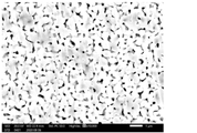
- the SEM image of the silver particle 1 is shown.
- the SEM cross-sectional photograph of the sintered body of Example 1 is shown.
- the SEM cross-sectional photograph of the sintered body of the comparative example 1 is shown.
- the cross-sectional SEM photograph of the sintered body of Example 3 is shown.
- a cross-sectional SEM photograph of the sintered body of Comparative Example 3 is shown.
- the cross-sectional SEM photograph of the sintered body after carrying out the thermal shock test of Example 3 for 300 cycles is shown.
- the cross-sectional SEM photograph of the sintered body after carrying out the thermal shock test of the comparative example 3 for 300 cycles is shown.
- the conductive adhesive of the present invention is a conductive adhesive containing silver particles 1 having an average particle diameter in the range of 20 nm or more and less than 500 nm and a solvent, and the water content of the solvent in the conductive adhesive is 1300 ppm. It is characterized by the following. Since the conductive adhesive of the present invention has such characteristics, it is suitably sintered at a low temperature without pressure when sintering the conductive adhesive, and has a high density and mechanical strength. It is possible to provide a novel conductive adhesive that forms a sintered body having high (shear strength).
- the conductive adhesive of the present invention the sintered body of the conductive adhesive, and the electronic components provided with the sintered body between the members will be described in detail.
- the numerical value connected by "-" means a numerical range including the numerical values before and after "-" as the lower limit value and the upper limit value.
- any lower limit value and upper limit value can be selected and connected by " ⁇ ".
- the conductive adhesive of the present invention is characterized by containing silver particles 1 having an average particle diameter in the range of 20 nm or more and less than 500 nm, and a solvent.
- the conductive adhesive contains a solvent, the fluidity of the conductive adhesive is increased, and the conductive adhesive of the present invention can be easily placed in a desired place. Details of the silver particles contained in the conductive adhesive of the present invention are as described below.
- the water content of the solvent in the conductive adhesive may be 1300 ppm or less.
- the water content of the solvent in the conductive adhesive may be 1300 ppm or less, preferably 1200 ppm or less, more preferably 1100 ppm or less, and even more preferably 1000 ppm or less.
- the lower limit of the water content of the solvent in the conductive adhesive may be not less than or equal to the measurement limit value of the method for measuring the water content, and may be, for example, 10 ppm or more.
- the above-mentioned effect can be obtained by setting the water content of the solvent in the conductive adhesive within the above range.
- the water content of the solvent in the conductive adhesive can be measured by gas chromatography, Karl Fischer method, or the like. Specifically, the water content of the solvent used for the conductive adhesive may be measured by the Karl Fischer method, and a solvent within the above range may be used.
- the water content in the solvent used for the conductive adhesive is adjusted to the conductive adhesive by using distillation, molecular sieve, alumina or the like. Those adjusted to 1300 ppm or less before addition can be used.
- some solvents in the conductive adhesive containing silver particles and a solvent have a water content reduced to 1300 ppm or less immediately after the purchase of a commercially available product. Such a water content Some have not been reduced to. Even when a solvent having a water content reduced to 1300 ppm or less is used, the solvent absorbs the water in the atmosphere in a short time during the production of the conductive adhesive, and the water content becomes high.
- the conductive adhesive of the present invention has a water content of 1300 ppm or less in the solvent in the conductive adhesive not only during production but also during use (specifically, when subjected to sintering). You are required to be.
- the water content of a conductive adhesive containing silver particles has not been strictly controlled so far, and a commercially available solvent having a water content adjusted to 1300 ppm or less has been used for producing the conductive adhesive.
- a solvent or a conductive adhesive may be sealed with dry air or nitrogen cylinder air during manufacturing, storage, distribution, or use. Further, the humidity of the living room at the time of use may be controlled.
- the silver particle 1 is in the range of 20 nm to 500 nm.
- the average particle size of the silver particles 1 may be in the range of 20 nm to 500 nm, but from the viewpoint of more preferably achieving the effect of the present invention, the lower limit is preferably 25 nm or more, more preferably 30 nm or more.
- the upper limit is preferably 500 nm or less, more preferably 450 nm or less, still more preferably 400 nm or less, and preferred ranges are 20 to 500 nm, 25 to 500 nm, 30 to 500 nm, 25 to 450 nm, 25 to 400 nm. Examples thereof include 30 to 450 nm and 30 to 400 nm.
- the average particle size of the silver particles 1 is a volume-based average particle measured for 200 randomly selected particles using image analysis software (for example, Macview (manufactured by Mountech)) for SEM images.
- image analysis software for example, Macview (manufactured by Mountech)
- the diameter For SEM observation, an SED mode (secondary electron detector) is used, and the acceleration voltage is 20 kV, and the observation magnification is 5000 to 30000 times, and the width is observed in the range of 1 to 20 ⁇ m. In the vertical direction of the SEM image, the width is set to include 200 or more (usually about 200 to 300) silver particles in a width range of 1 to 20 ⁇ m.
- the volume-based average particle diameter is a value measured on the assumption that the particles observed in the SEM image are spherical having the diameter. The specific measurement method is as described in the examples.
- the dry powder of the silver particles 1 preferably has a weight loss rate of 1.5% by weight or less when heated from 30 ° C. to 500 ° C. by thermogravimetric differential thermal analysis, preferably 0.05 to 1.3% by weight. % Is more preferable.
- the method of thermogravimetric differential thermal analysis is as follows.
- TG-DTA Thermogravimetric differential thermal analysis
- the silver particles 1 are preferably surface-treated silver particles.
- the amine compound is attached to the surface of the silver particles 1.
- the amine compound can adhere to the surface of the silver particles 1 to form a protective layer.
- the amine compound is not particularly limited, but from the viewpoint of more preferably exerting the effect of the present invention, a primary amine, a secondary amine, a tertiary amine, and two amino groups in one compound are used. Examples thereof include diamine compounds having.
- Primary amines include ethylamine, n-propylamine, isopropylamine, 1,2-dimethylpropylamine, n-butylamine, isobutylamine, sec-butylamine, tert-butylamine, isoamylamine, n-hexylamine, n- Octylamine, 2-octylamine, tert-octylamine, 2-ethylhexylamine, n-nonylamine, n-aminodecane, n-aminoundecane, n-dodecylamine, n-tridecylamine, 2-tridecylamine, n- Tetradecylamine, n-pentadecylamine, n-hexadecylamine, n-heptadecylamine, n-octadecylamine, n-oleylamine, 3-methoxypropy
- cyclopropylamine, cyclobutylamine, cyclopropylamine, cyclohexylamine, cycloheptylamine, cyclooctylamine which are alicyclic amines, aniline which is an aromatic amine and the like can also be exemplified.
- ether amines such as 3-isopropoxypropylamine and isobutoxypropylamine can also be exemplified.
- Secondary amines include N, N-dipropylamine, N, N-dibutylamine, N, N-dipentylamine, N, N-dihexylamine, N, N-dipeptylamine, N, N-dioctylamine, N.
- N-dinonylamine N, N-didecylamine, N, N-diundecylamine, N, N-didodecylamine, N, N-dystearylamine, N-methyl-N-propylamine, N-ethyl-N- Dialkyl monoamines such as propylamine and N-propyl-N-butylamine, and cyclic amines such as piperidine can be exemplified.
- tertiary amine examples include triethylamine, tributylamine, trihexylamine, dimethyloctylamine, dimethyldecylamine, dimethyllaurylamine, dimethylmyristylamine, dimethylpalmitylamine, dimethylstearylamine, dilaurylmonomethylamine and the like.
- amine compound a diamine compound having two amino groups in one compound can also be used.
- diamine compound include ethylenediamine, N, N-dimethylethylenediamine, N, N'-dimethylethylenediamine, N, N-diethylethylenediamine, N, N'-diethylethylenediamine, 1,3-propanediamine, and 2,2-dimethyl-.
- 1,3-Propanediamine N, N-dimethyl-1,3-propanediamine, N, N'-dimethyl-1,3-propanediamine, N, N-diethyl-1,3-propanediamine, N, N '-Diethyl-1,3-propanediamine, 1,4-butanediamine, N, N-dimethyl-1,4-butanediamine, N, N'-dimethyl-1,4-butanediamine, N, N-diamine -1,4-butanediamine, N, N'-diethyl-1,4-butanediamine, 1,5-pentanediamine, 1,5-diamino-2-methylpentane, 1,6-hexanediamine, N, N Examples thereof include -dimethyl-1,6-hexanediamine, N, N'-dimethyl-1,6-hexanediamine, 1,7-heptanediamine, 1,8-octanediamine and the like.
- the amount of the amine compound attached to the silver particles 1 is not particularly limited, but the mass of the silver particles 1 is 100% by mass, preferably 1.5% by mass or less, more preferably 1.3% by mass or less, and the lower limit. Is preferably 0.05% by mass or more.
- the content of the amine compound adhering to the silver particles 1 can be measured by thermogravimetric differential thermal analysis.
- fatty acids, hydroxy fatty acids and the like may be attached to the surface of the silver particles 1.
- the fatty acid is not particularly limited, but preferably includes a fatty acid having an alkyl group having 3 or more and 18 or less carbon atoms, and more preferably a fatty acid having an alkyl group having 4 or more and 18 or less carbon atoms.
- Preferred specific examples of fatty acids include acetic acid, propionic acid, butyric acid, valeric acid, caproic acid, caprylic acid, 2-ethylhexanoic acid, caproic acid, lauric acid, myristic acid, palmitic acid, stearic acid, oleic acid and linoleic acid.
- Examples thereof include acid, ⁇ -linolenic acid and the like.
- specific examples of the fatty acid include cyclic alkylcarboxylic acids such as cyclohexanecarboxylic acid.
- a compound having 3 to 24 carbon atoms and having one or more hydroxyl groups can be used.
- examples of the hydroxy fatty acid include 2-hydroxydecanoic acid, 2-hydroxydodecanoic acid, 2-hydroxytetradecanoic acid, 2-hydroxyhexadecanoic acid, 2-hydroxyoctadecanoic acid, 2-hydroxyeicosanoic acid and 2-hydroxydocosan.
- hydroxy fatty acids having 4 to 18 carbon atoms and having one hydroxyl group other than the ⁇ -position are preferable, and ricino-lic acid, 12-hydroxystearic acid, and oleic acid are more preferable.
- the fatty acid and the hydroxy fatty acid may be used individually by 1 type, or may be used in combination of 2 or more types.
- the amount of fatty acid or hydroxy fatty acid attached to the silver particles 1 of the present invention is appropriately adjusted as in the case of the amine compound.
- the specific amount of the fatty acid or hydroxy fatty acid attached is not particularly limited, but the mass of the silver particles 1 is 100% by mass, preferably 1.5% by mass or less, more preferably 1.3% by mass or less, and is preferable. Is 0.01% by mass or more.
- the content of fatty acid and hydroxy fatty acid adhering to the silver particles 1 can be measured by differential thermal analysis.
- the amine compound, fatty acid, and hydroxy fatty acid may be used in combination as long as the silver particles 1 of the present invention satisfy the above average particle size, and other compounds different from these may be used as silver particles 1. It may be attached to the surface of. It is particularly preferable that an amine compound is attached to the surface of the silver particles 1 of the present invention.
- silver particles having an average particle diameter of 20 to 500 nm may be used alone, or a plurality of silver particles having an average particle diameter of 20 to 500 nm may be used in combination.
- the ratio when a plurality of silver particles having an average particle diameter of 20 to 500 nm are used in combination may be appropriately adjusted so as to obtain the desired physical properties.
- the average particle diameter is in the range of 20 to 500 nm.
- silver particles 1a having a small size and silver particles 1b having a large average particle size are used, the ratio of the silver particles 1a to the silver particles 1b may be in the range of 1 to 30:70 to 99.
- the conductive adhesive of the present invention may contain silver particles 2 having an average particle diameter of 20 to 500 nm as described above, as well as silver particles 2 having an average particle diameter of 0.5 to 5.5 ⁇ m, if necessary. good.
- the average particle size of the silver particles 2 is preferably 0.6 ⁇ m or more as the lower limit and preferably 3.0 ⁇ m or less, more preferably as the upper limit, from the viewpoint of more preferably exerting the effect of the present invention. 2.5 ⁇ m or less, more preferably 2.0 ⁇ m or less, and preferred ranges of 0.5 to 3.0 ⁇ m, 0.5 to 2.5 ⁇ m, 0.5 to 2.0 ⁇ m, and 0.6 to 3 Examples thereof include 0.0 ⁇ m, 0.6 to 2.5 ⁇ m, and 0.6 to 2.0 ⁇ m.
- the average particle size of the silver particles 2 can be measured by a laser diffraction / scattering method particle size distribution measuring device, or can be actually measured from an electron micrograph, and further, an image from the electron micrograph. It can also be calculated using a processing device. Generally, the average particle size is measured by a laser diffraction method or image analysis of an SEM image (for example, Macview (manufactured by Mountech)).
- silver particles 2 in the present invention commercially available ones may be used, or those synthesized by a known synthesis method may be used.
- the silver particles 1 may be used alone or the silver particles 1 and the silver particles 2 may be used in combination as the silver particles.
- the ratio of silver particles 1 to silver particles 2 may be in the range of (silver particles 1: silver particles 2) 30 to 70: 70 to 30, and 35 to 35.
- the range of 65:65 to 35 is preferable, and the range of 40 to 60:60 to 40 is more preferable.
- the solvent is not particularly limited as long as it can have a water content of 1300 ppm or less and can disperse silver particles, but it is preferable to include a polar organic solvent.
- the polar organic solvent include ketones such as acetone, acetylacetone and methyl ethyl ketone; ethers such as diethyl ether, dipropyl ether, dibutyl ether, tetrahydrofuran and 1,4-dioxane; 1,2-propanediol.
- Glycols or glycolethers such as; N, N-dimethylformamide; dimethylsulfoxide; terpenes such as terpineol; acetonitrile; ⁇ -butyrolactone; 2-pyrrolidone; N-methylpyrrolidone; N- (2). -Aminoethyl) Piperazine and the like.
- linear or branched alcohol having 3 to 5 carbon atoms, 3-methoxy-3-methyl-1-butanol, 3-methoxy.
- the solvent may further contain a non-polar or hydrophobic solvent in addition to the polar organic solvent.
- Non-polar organic solvents include linear, branched, or cyclic saturated hydrocarbons such as hexane, heptane, octane, nonane, decane, 2-ethylhexane, cyclohexane; linear or branched alcohols with 6 or more carbon atoms.
- -Alcohols such as benzene; aromatic compounds such as benzene, toluene and benzonitrile; halogenated hydrocarbons such as dichloromethane, chloroform and dichloroethane; methyl-n-amylketone; methylethylketone oxime; triacetin and the like.
- saturated hydrocarbons and straight-chain or branched-chain alcohols having 6 or more carbon atoms are preferable, and hexane, octane, decane, octanol, decanol, and dodecanol are more preferable.
- the solvent one type can be used alone, or two or more types can be mixed and used.
- the ratio of the polar organic solvent is preferably 5% by volume or more, more preferably 10% by volume or more, and further preferably 15% by volume or more with respect to the total amount of the solvent. More preferred. Further, it can be 60% by volume or less, 55% by volume or less, or 50% by volume or less.
- the solvent may be composed of only a polar organic solvent.
- the conductive adhesive of the present invention has good dispersibility of silver particles even when it contains a large amount of polar organic solvent as described above.
- the ratio of the solvent is not particularly limited, but is preferably 20% by mass or less, and more preferably about 5% by mass to 15% by mass.
- the content of silver particles contained in the conductive adhesive of the present invention is preferably 80% by mass or more, more preferably 85% by mass or more.
- the conductive adhesive of the present invention can be produced by a method including a step of mixing each silver particle and a solvent.
- the silver particles of the present invention produced in a solvent are used together with the solvent as the conductive adhesive of the present invention. May be good.
- the shear strength of the sintered body obtained by heating the conductive adhesive at 200 ° C. is preferably 35 MPa or more, more preferably 40 MPa or more, still more preferably 45 MPa or more. be.
- the upper limit of the shear strength is, for example, 200 MPa or less.
- the shear strength of the sintered body obtained by heating the conductive adhesive at 250 ° C. is preferably 30 MPa or more, more preferably 35 MPa or more. Yes, more preferably 40 MPa or more.
- the upper limit of the shear strength is, for example, 200 MPa or less.
- the method for measuring the shear strength of the sintered body is as follows, and specifically, it is measured by the method described in Examples.
- a substrate having electroless silver plating of 0.5 ⁇ m on a copper plate is prepared.
- Conductive adhesive (90% by mass of silver particles, solvent (for example, diethylene glycol mono-2-ethylhexyl ether, texanol, etc.) 10% by mass of silver particle dispersion on the base material (surface on which silver plating is formed)) Is uniformly applied so that the coating thickness is 50 to 100 ⁇ m (adjusted by the thickness of the bonded body after plating).
- a silicon wafer size 2 mm ⁇ 2 mm
- gold plating on the back surface the surface in contact with the conductive adhesive
- the obtained laminate is heated at a predetermined sintering temperature (200 ° C. or 250 ° C.) under sintering conditions for 60 minutes, and is placed between the substrate and the silicon wafer.
- a predetermined sintering temperature 200 ° C. or 250 ° C.
- Each conductive adhesive is sintered, and nine laminated bodies in which a base material and a silicon wafer are bonded via a sintered body are produced.
- the thickness of the bonded body is 30 to 90 ⁇ m, and the film thicknesses of the conductive adhesives to be compared are made uniform and compared.
- a bond tester for example, SS30-WD manufactured by Seishin Shoji
- SS30-WD manufactured by Seishin Shoji
- a die share test of each laminate was performed.
- the shear strength value is obtained by dividing the maximum load thus obtained by the joint area.
- the measurement result is an average value of nine gold-plated silicon wafers whose shear strength was measured.
- the sintering time at a predetermined sintering temperature may be 60 minutes or more, and pre-baking may be performed at 50 to 100 ° C. for 2 hours or less before the main sintering at a predetermined sintering temperature. ..
- the density of the sintered body obtained by heating the conductive adhesive at 200 ° C. is preferably 80% or more, more preferably 85% or more.
- the upper limit of the density is, for example, 95% or less.
- the density of the sintered body obtained by heating the conductive adhesive at 250 ° C. is preferably 83% or more, more preferably 85%. That is all.
- the upper limit of the density is, for example, 97% or less.
- the method for measuring the density of the sintered body is as follows, and specifically, it is measured by the method described in Examples.
- ⁇ Denseness> In the same manner as described in the column of ⁇ shear strength>, a laminated body in which a base material and a silicon wafer are bonded via a sintered body is obtained. Next, the sintered body is embedded with an epoxy resin (for example, manufactured by Buehler) together with the laminated body, and allowed to stand for 24 hours to cure the resin. Next, the resin-embedded laminate is cut with a precision low-speed cutting machine (for example, TechCut4 manufactured by ALLIED) and ion milling (for example, IM4000PLUS manufactured by Hitachi High-Technologies Corporation) (for example, IM4000PLUS manufactured by Hitachi High-Technologies Corporation). , Perform cross-section milling.
- a precision low-speed cutting machine for example, TechCut4 manufactured by ALLIED
- ion milling for example, IM4000PLUS manufactured by Hitachi High-Technologies Corporation
- IM4000PLUS manufactured by Hitachi High-Technologies Corporation for example, IM
- the cross-sectional milling is carried out by irradiating an ion beam with an argon gas flow rate of 0.07 cm 3 / min and a swing of ⁇ 30 ° at a discharge voltage of 1.5 kV and an acceleration voltage of 6 kV.
- the cross section of the sintered body obtained by cross-section milling is observed with a scanning electron microscope to obtain an SEM image.
- the SED mode secondary electron detector
- the vertical direction of the SEM image shall be in the range of the vertical width of the silver sintered layer of 30 ⁇ m or more and 200 ⁇ m or less.
- Dense density (%) Sintered silver area (number of white pixels) ⁇ Total area of sintered body ⁇ Sintered silver area (number of white pixels) + pore area (number of black pixels) ⁇ x 100
- the void portion is a pore portion generated by outgas or particle growth, which is different from voids and cracks, and the pore portion has a diameter of 50 nm or more and 10 ⁇ m or less. Holes having a diameter of more than 10 ⁇ m and having a connected size due to continuous voids are called voids or cracks, and are converted by excluding the void portion.
- the voids of the sintered body obtained by heating the conductive adhesive at 200 ° C. have, for example, the following characteristics.
- the sintered body is formed by the method described in the column of ⁇ shear strength>.
- the average size of the number of voids is, for example, 0.3 to 1.1 ⁇ m.
- the specific surface area of the void is, for example, 0.15 to 1.0 ⁇ m 2 .
- the size of the number average is calculated by the image processing method using Macview.
- a composition for producing silver particles (a composition for preparing silver particles) is prepared.
- a silver compound as a raw material for silver particles, an amine compound to be adhered to the surface of silver particles, and a solvent are prepared, if necessary.
- preferred silver compounds include silver nitrate, silver oxalate and the like, and silver oxalate is particularly preferable.
- the solvent the same solvent as that exemplified as the solvent to be blended in the conductive adhesive described later is exemplified.
- each of these components is mixed to obtain a composition for preparing silver particles. The ratio of each component in the composition is appropriately adjusted.
- the content of silver oxalate in the composition is preferably about 20 to 70% by mass with respect to the total amount of the composition.
- the content of the amine compound is preferably about 5% by mass to 55% by mass with respect to the total amount of the composition.
- the fatty acid content is preferably about 0.1% by mass to 20% by mass with respect to the total amount of the composition.
- the content of the hydroxy fatty acid is preferably about 0.1% by mass to 15% by mass with respect to the total amount of the composition.
- silver particles are once synthesized using a composition for preparing silver particles adjusted so that the content of the amine compound or the like is out of the above range, and the type and the amount of the amine compound or the like are determined by the method described later. It is also possible to adjust (substitute the amine compound) so as to have the above physical properties.
- the mixing means of each component is not particularly limited, and for example, a mechanical star, a magnetic star, a vortex mixer, a planetary mill, a ball mill, a triple roll, a line mixer, and a planetary. It can be mixed with a general-purpose device such as a mixer or a dissolver.
- a general-purpose device such as a mixer or a dissolver.
- the temperature of the composition is set to, for example, 60 ° C. or lower, particularly 40 ° C. It is preferable to mix while suppressing the following.
- the composition for preparing silver particles by subjecting the composition for preparing silver particles to a reaction in a reaction vessel, usually a reaction by heating, a thermal decomposition reaction of the silver compound occurs and silver particles are generated.
- the composition may be introduced into a reaction vessel that has been preheated, or the composition may be introduced into the reaction vessel and then heated.
- the reaction temperature may be any temperature as long as the thermal decomposition reaction proceeds and silver particles are generated, and examples thereof include about 50 to 250 ° C. Further, the reaction time may be appropriately selected according to the desired average particle size and the composition of the composition accordingly. Examples of the reaction time include 1 minute to 100 hours.
- the silver particles produced by the thermal decomposition reaction are obtained as a mixture containing unreacted raw materials, it is preferable to purify the silver particles.
- the purification method include a solid-liquid separation method, a precipitation method using a difference in specific gravity between silver particles and an unreacted raw material such as an organic solvent, and the like.
- the solid-liquid separation method include filter-filtration, centrifugation, cyclone method, decanter and the like.
- the viscosity of the mixture containing silver particles may be adjusted by diluting the mixture containing silver particles with a low boiling point solvent such as acetone or methanol for ease of handling during purification.
- the average particle size of the obtained silver particles can be adjusted by adjusting the composition and reaction conditions of the composition for producing silver particles.
- Silver particles (with an amine compound attached to the surface) once synthesized by the above method are prepared and dispersed in a solvent.
- a solvent the same solvent as that exemplified as the solvent to be blended in the conductive adhesive described later is exemplified.
- another amine compound is added in a range of 0.1 to 5 times the mass of the silver particles, and the mixture is subjected to a step of stirring at room temperature to 80 ° C. for 1 minute to 24 hours.
- the type of amine compound adhering to the surface of the silver particles can be replaced, and the amount of adhering can be adjusted.
- the silver particles substituted with the amine compound can be recovered by the above-mentioned solid-liquid separation method or the like.
- the sintered body of the conductive adhesive of the present invention can be obtained by sintering the conductive adhesive of the present invention described in detail in "1. Conductive adhesive" described above. .. In the sintered body of the conductive adhesive of the present invention, most of the components (amine compounds, etc.) and solvents adhering to the surface of the silver particles are separated due to the high heat during sintering, and the sintering is performed.
- the body is essentially composed of silver.
- the sintering temperature is not particularly limited, but is, for example, 250 ° C. or lower, preferably about 150 ° C. to 250 ° C., from the viewpoint of increasing the shear strength and the density of the obtained sintered body while suitably sintering at a low temperature. More preferably, it is about 200 ° C. to 250 ° C. From the same viewpoint, the sintering time is preferably about 0.4 hours to 2.0 hours, more preferably about 0.5 hours to 1.5 hours.
- the sintering time refers to the main sintering (maintained at the predetermined temperature after reaching the predetermined temperature) time, and other than that, pre-baking (before reaching the predetermined temperature, 100 ° C. or less).
- the conductive adhesive contains silver particles 1 having an average particle diameter in the range of 20 to 500 nm and a solvent, and the water content of the solvent in the conductive adhesive is 1300 ppm or less.
- it is suitably sintered at a low temperature of 250 ° C. or lower without pressurizing when sintering the conductive adhesive, and a sintered body having high density and mechanical strength (shear strength) is formed. Will be done. Therefore, it is not essential to pressurize when sintering the conductive adhesive of the present invention. That is, the conductive adhesive of the present invention can be suitably used for applications in which it is used without pressure during sintering.
- the pressure may be applied during the sintering of the conductive adhesive of the present invention, and the pressure when the pressure is applied is, for example, about 10 to 30 MPa.
- Sintering can be performed in an atmosphere such as an atmosphere or an inert gas (nitrogen gas, argon gas).
- the sintering means is not particularly limited, and examples thereof include an oven, a hot air drying oven, an infrared drying oven, laser irradiation, flash lamp irradiation, and microwave.
- the sintered body of the conductive adhesive of the present invention can be obtained by uniformly coating a substrate on a substrate and sintering it at a predetermined temperature, but the film thickness when coated on the substrate depends on the purpose. It can be adjusted as appropriate, and may be, for example, a thickness of about 10 to 100 ⁇ m. Further, when a large-sized (for example, about 10 mm ⁇ 10 mm) semiconductor chip is used, a thicker one is preferred. Therefore, the film thickness when applied to the substrate may be, for example, 30 ⁇ m or more, and 40 ⁇ m. The above is preferable, and 50 ⁇ m or more is more preferable. In this case, the upper limit of the film thickness may be 200 ⁇ m or less, preferably 100 ⁇ m or less.
- the sintered body of the present invention preferably satisfies at least one of the shear strength and the density shown in the column of "1.
- Conductive adhesive These measuring methods are as described in the columns of ⁇ shear strength> and ⁇ dense density> described above.
- the electronic components of the present invention include a portion in which the members are adhered to each other by the sintered body of the present invention. That is, in the electronic component of the present invention, the conductive adhesive of the present invention described in detail in the above-mentioned "1. Conductive adhesive" is arranged between the members of the electronic component (for example, between the members included in the circuit). , The conductive adhesive is sintered and the members are bonded together.
- the sintered body of the present invention has high precision density and shear strength, the shear strength between the members is also high even in the electronic component provided with the sintered body. Further, the resistivity value of the electronic component of the present invention can also be low.
- Solvent 1 Texanol (manufactured by Fujifilm Wako Pure Chemical Industries, Ltd.) Solvent 2) ⁇ -Tarpineol (manufactured by Fujifilm Wako Pure Chemical Industries, Ltd.) Solvent 3) Diethylene glycol mono-2-ethylhexyl ether (manufactured by Fujifilm Wako Pure Chemical Industries, Ltd.) Solvent 4) Butyl carbitol (manufactured by Fujifilm Wako Pure Chemical Industries, Ltd.) Solvent 5) Hexylcarbitol (manufactured by Fujifilm Wako Pure Chemical Industries, Ltd.) Solvent 6) 2-Ethyl-1,3-hexanediol (manufactured by Fujifilm Wako Pure Chemical Industries, Ltd.)
- Silver particles 1 (average particle diameter 68 nm) in which the protective layer adhering to the surface of silver particles was replaced with n-hexylamine by repeating the steps of adding 15 g of metalnol, stirring, centrifuging, and removing the supernatant twice. was recovered.
- FIG. 1 shows an SEM image of silver particles 1.
- Silver particles 3 (average particle diameter 440 nm) in which the protective layer adhering to the surface of the silver particles was replaced with n-hexylamine by repeating the steps of adding 15 g of metalnol, stirring, centrifuging, and removing the supernatant twice. was recovered.
- a conductive adhesive was prepared by mixing silver particles 1 and a solvent (diethylene glycol mono-2-ethylhexyl ether, texanol, or hexylcarbitol) so as to have the composition (mass ratio) shown in Table 2. .. Specifically, first, for silver particles 1, 10% by mass of diethylene glycol mono-2-ethylhexyl ether, texanol, or hexylcarbitol is added to each silver particle dispersion having a concentration of 90% by mass (1).
- a solvent diethylene glycol mono-2-ethylhexyl ether, texanol, or hexylcarbitol
- Silver particle dispersion 1-1 diethylene glycol mono-2-ethylhexyl ether, silver particle dispersion 1-2: texanol, silver particle dispersion 1-3: hexylcarbitol) were prepared, respectively.
- a Mazelstar manufactured by Kurabo Industries Ltd. was used, and the mixture was mixed in the two-time stirring priority mode.
- each conductive adhesive having the compositions of Examples 1 to 2 and 4 and Comparative Examples 1 to 2 and 4 was obtained.
- a solvent diethylene glycol mono-2-ethylhexyl ether; water content of 150 ppm or less, texanol; water content of 100 ppm or less; Hexylcarbitol; water content of 100 ppm or less
- a solvent whose water content was not adjusted diethylene glycol mono-2-ethylhexyl ether; water content of 1700 ppm or less, texanol; water content of 1360 ppm
- hexylcarbitol a water content of 2000 ppm or less
- the water content of the solvent used in the examples was measured by the method described later.
- composition (mass ratio) shown in Table 2 is such that silver particles 1, silver particles 2 having an average particle diameter of 0.65 ⁇ m (product name AG2-1C manufactured by DOWA Electronics Co., Ltd.), and a solvent (texano-). Lu) was mixed to prepare a conductive adhesive. Specifically, first, for each of the silver particles 1 and the silver particles 2, 10% by mass of texanol is added, and each silver particle dispersion having a concentration of 90% by mass (silver particle dispersion 1-2, A silver particle dispersion 2) was prepared. For mixing, a Mazelstar manufactured by Kurabo Industries Ltd. was used, and the mixture was mixed in the two-time stirring priority mode.
- each silver particle dispersion and texanol are mixed so as to have the composition (mass ratio) shown in Table 2, and each conductive adhesive having the composition of Example 3 and Comparative Example 3 is prepared. Obtained.
- 100 g of a molecular sieve was used with respect to 1000 g of the solvent, a solvent having an adjusted water content (texanol; a water content of 100 ppm or less) was used, and in the comparative example, a solvent having no adjusted water content. (Texanol; water content of 1360 ppm or less) was used. The water content of the solvent used in the examples was measured by the method described later.
- ⁇ Measuring method of water content of solvent in conductive adhesive The moisture content of the solvent in the conductive adhesive was measured using a Karl Fischer type moisture meter CA-21 (manufactured by Nittoseiko Analytec). Specifically, 0.200 g of the solvent is directly injected into the moisture meter cell, and the water content detected when the detected amount is less than 0.30 ⁇ g / s is set as the end point, and the water content of the solvent is calculated from the water detected amount / solvent injection amount. The content was calculated.
- a substrate having electroless silver plating of 0.5 ⁇ m on a copper plate was prepared.
- Each conductive adhesive was uniformly applied onto the substrate (the surface on which silver plating or gold plating was formed) so that the coating film thickness was 50 to 100 ⁇ m.
- a silicon wafer (size 2 mm ⁇ 2 mm) having gold plating on the back surface (the surface in contact with the conductive adhesive) was laminated on the coating film to obtain a laminate.
- the obtained laminate is heated at a predetermined sintering temperature (200 ° C.) under sintering conditions for 60 minutes, and each conductivity between the substrate and the silicon wafer is obtained.
- the adhesive was sintered, and nine laminates were obtained in which the base material and the silicon wafer were bonded via the sintered body.
- the thickness of the sintered body after sintering was 30 ⁇ m to 90 ⁇ m.
- Table 3 shows the results of Example 1, Comparative Example 1, Table 4 shows the results of Example 2, Comparative Example 2, Table 5 shows the results of Example 3, Comparative Example 3, and Table 6 shows the results of Example 4 and Comparative Example 4.
- the cross-sectional milling was carried out by irradiating an ion beam with an argon gas flow rate of 0.07 cm 3 / min and a swing of ⁇ 30 ° at a discharge voltage of 1.5 kV and an acceleration voltage of 6 kV.
- the cross section of the sintered body obtained by cross-section milling was observed with a scanning electron microscope JSM-IT500HR (manufactured by JEOL Ltd.) to obtain an SEM image.
- the SED mode secondary electron detector
- the range of the width of 10 ⁇ m was observed in the field of view of the acceleration voltage of 20 kV and 10000 times.
- Dense density (%) Sintered silver area (number of white pixels) ⁇ Total area of sintered body ⁇ Sintered silver area (number of white pixels) + pore area (number of black pixels) ⁇ x 100
- FIG. 2 shows a cross-sectional SEM photograph of the sintered body of Example 1
- FIG. 3 shows a cross-sectional SEM photograph of the sintered body of Comparative Example 1
- FIG. 4 shows the sintered body of Example 3.
- a cross-sectional SEM photograph of the above, and FIG. 5 shows a cross-sectional SEM photograph of the sintered body of Comparative Example 3.
- the conductive adhesive of Example 1 in which the water content of the solvent in the conductive adhesive is controlled to 1300 ppm or less is at a low temperature even if it is not pressed during sintering of the conductive adhesive.
- a sintered body having high density and mechanical strength (shear strength) was formed.
- the conductive adhesive of Comparative Example 1 in which the water content of the solvent in the conductive adhesive exceeds 1300 ppm has a lower shear strength of the obtained sintered body as compared with Example 1, and is baked. Cracks and chips were found in the body, and voids and cracks were observed. It is considered that this is largely due to the decrease in the fineness of the sintered body and the deterioration of the sinterability of the silver particles 1.
- the sintered body of Comparative Example 1 had many cracks and chips and had a low density.
- the conductive adhesive of Example 2 in which the water content of the solvent in the conductive adhesive is controlled to 1300 ppm or less is at a low temperature even if it is not pressed during sintering of the conductive adhesive. A sintered body having high density and mechanical strength (shear strength) was formed.
- the conductive adhesive of Comparative Example 2 in which the water content of the solvent in the conductive adhesive exceeds 1300 ppm has a lower shear strength of the obtained sintered body as compared with Example 2, and is baked. Cracks and chips were found in the body, and voids and cracks were observed.
- Example 3 ⁇ Cold heat impact test of sintered body>
- the laminates obtained in Example 3 and Comparative Example 3 were subjected to a thermal shock test in which they were held at ⁇ 65 ° C. to 150 ° C. for 10 minutes, respectively, for 300 cycles.
- Table 5 shows the results of shear strength measurements before and after the test.
- the bonding state of the interface between the sintered body and the silicon wafer was observed from the SEM cross section of the sintered body after the test. Those with a good interface bonding state were rated as ⁇ , and those with a poor interface bonding state were rated as x.
- FIG. 6 shows a cross-sectional SEM photograph of the sintered body after 300 cycles of the cold shock test of Example 3
- FIG. 7 shows a cross-sectional SEM photograph of the sintered body after 300 cycles of the cold shock test of Comparative Example 3.
- the sintered body of Example 3 did not crack and chipped, and the bonded state at the interface between the sintered body and the silicon wafer after the thermal impact test was good.
- the sintered body of Comparative Example 3 had cracks and chips, and the bonding state at the interface between the sintered body and the silicon wafer after the thermal impact test was poor.
- Even in a system in which silver particles 2 are mixed it has a great influence on the formation of the sintered body and lowers the initial shear strength and the shear strength after the thermal impact test. It is considered that this is because the density of the interface between the silver sintered body and the silicon wafer was particularly low.
- the conductive adhesive of Example 4 in which the water content of the solvent in the conductive adhesive is controlled to 1300 ppm or less is at a low temperature even if it is not pressed during sintering of the conductive adhesive.
- a sintered body having high density and mechanical strength (shear strength) was formed.
- the conductive adhesive of Comparative Example 4 in which the water content of the solvent in the conductive adhesive exceeds 1300 ppm is found in the case where the obtained sintered body also has a large amount of water as compared with Example 4. The shear strength decreased, and cracks and chips were generated in the sintered body, and voids and cracks were observed.
- a conductive adhesive is prepared by mixing silver particles 3 (average particle diameter 440 nm) and a solvent (diethylene glycol mono-2-ethylhexyl ether or texanol) so as to have the composition (mass ratio) shown in Table 7.
- a solvent diethylene glycol mono-2-ethylhexyl ether or texanol
- Dispersion 3-1 diethylene glycol mono-2-ethylhexyl ether
- silver particle dispersion 3-2 texanol
- each conductive adhesive having the compositions of Examples 5 to 6 and Comparative Examples 5 to 6 was obtained.
- 100 g of a molecular sieve was used with respect to 1000 g of the solvent, and the water content was adjusted (diethylene glycol mono-2-ethylhexyl ether; water content 130 ppm or less, texanol; water content 130 ppm or less).
- a solvent having no adjusted water content (diethylene glycol mono-2-ethylhexyl ether; water content of 5000 ppm or less, texanol; water content of 5400 ppm or less) was used.
- the water content of the solvent used in the examples was measured by the method described above.
- a sintered body was produced from each conductive adhesive by the same method as in Example 1 and Comparative Example 1.
- Various physical properties of each sintered body obtained from the conductive adhesive were measured under the above-mentioned measurement conditions.
- Table 8 shows the results of Example 5, Comparative Example 5, and Table 9 shows the results of Example 6 and Comparative Example 6.
- the conductive adhesive of Example 5 in which the water content of the solvent in the conductive adhesive is controlled to 1300 ppm or less is at a low temperature even if it is not pressed during sintering of the conductive adhesive. A sintered body having high density and mechanical strength (shear strength) was formed.
- the conductive adhesive of Comparative Example 5 in which the water content of the solvent in the conductive adhesive exceeds 1300 ppm has a lower shear strength of the obtained sintered body as compared with Example 2, and is baked. Cracks and chips were found in the body, and voids and cracks were observed.
- the conductive adhesive of Example 6 in which the water content of the solvent in the conductive adhesive was controlled to 1300 ppm or less is at a low temperature even if it is not pressed during sintering of the conductive adhesive. A sintered body having high density and mechanical strength (shear strength) was formed.
- the conductive adhesive of Comparative Example 6 in which the water content of the solvent in the conductive adhesive exceeds 1300 ppm has a lower shear strength of the obtained sintered body as compared with Example 6, and is baked. Cracks and chips were found in the body, and voids and cracks were observed.
Landscapes
- Chemical & Material Sciences (AREA)
- Organic Chemistry (AREA)
- Engineering & Computer Science (AREA)
- Inorganic Chemistry (AREA)
- Mechanical Engineering (AREA)
- Materials Engineering (AREA)
- Chemical Kinetics & Catalysis (AREA)
- Nanotechnology (AREA)
- Composite Materials (AREA)
- Manufacturing & Machinery (AREA)
- Dispersion Chemistry (AREA)
- Polymers & Plastics (AREA)
- Medicinal Chemistry (AREA)
- Health & Medical Sciences (AREA)
- General Chemical & Material Sciences (AREA)
- Metallurgy (AREA)
- Physics & Mathematics (AREA)
- Spectroscopy & Molecular Physics (AREA)
- Conductive Materials (AREA)
- Powder Metallurgy (AREA)
Abstract
導電性接着剤とした場合に、導電性接着剤の焼結の際に加圧しなくとも、低温において好適に焼結され、緻密度及び機械的強度(せん断強度)の高い焼結体が形成される、導電性接着剤を提供する。 平均粒子径が20nm以上500nm未満の範囲である銀粒子と、溶媒を含む、導電性接着剤であって、導電性接着剤における水分含有量が1300ppm以下である、導電性接着剤。
Description
本発明は、導電性接着剤、当該導電性接着剤の焼結体、及び当該焼結体を部材間に備えている電子部品に関する。
ダイボンド剤等を始めとする導電性接着剤は、半導体、LED、パワ-半導体等の電子部品に使われる接合材料である。接合方式として、加圧と加熱による接合、もしくは無加圧で加熱等による焼結によって基材と接合させることが一般に知られている。近年、製造プロセスの簡便さや効率の観点から、無加圧方式の接合材料の開発が進んでいる。
無加圧方式の接合材料として、一つはエポキシ樹脂を含む導電性接着剤が挙げられる。この接合材料は、低温処理でエポキシ樹脂を硬化させて使用するものであり、ボイド発生の抑制や基材との接合強度を向上させることができる(特許文献1)。しかしながら、エポキシ樹脂自体が抵抗体となるために、得られる導電性や熱伝導性が低くなる。
一方、エポキシ樹脂等の熱硬化性樹脂を含まない接合材料として、近年、銀粒子の開発が進んでいる。銀粒子は、低温で短時間の熱処理で容易に焼結する特徴がある。例えば、特許文献2には、銀粒子からなる固形分と溶媒とを混練してなる金属ペ-ストにおいて、前記固形分が、粒径100~200nmの銀粒子を粒子数基準で30%以上含む銀粒子で構成されており、更に、固形分を構成する銀粒子は、保護剤として炭素数の総和が4~8のアミン化合物が結合した金属ペ-ストが開示されている。当該金属ペ-ストによれば、低温域で銀粒子を焼結させることができ、その上で抵抗の低い焼結体や熱伝導性に優れた焼結体を形成可能とされている。
導電性接着剤の分野において、導電性接着剤を部材(例えば、電子部品に使用される基板、半導体チップ等)に塗布、焼結して得られる焼結体の空隙を少なくする(緻密度を高くする)ために、焼結時に加圧する(圧力は例えば10~30MPa程度)ことが一般的に行われている。導電性接着剤を加圧しながら焼結することで、焼結体の空隙を少なくすることができる。なお、焼結体中に空隙が多い場合、機械的強度(せん断強度)が不十分になったり、焼結体に割れや欠けが生じやすい等、信頼性の点で問題となる。一方で、焼結時の加圧により、導電性接着剤を塗布した部材にダメ-ジを与える、加圧のために特殊な設備が必要となる等の問題点も挙げられる。また、複雑構造を有する半導体チップ等に焼結体を形成する場合には、導電性接着剤を加圧することができないという問題もある。
そこで、焼結時に加圧を行わなくとも、緻密度、及び機械的強度(せん断強度)の高い焼結体が形成される、導電性接着剤の開発が求められている。
さらに、導電性接着剤は、一般に300℃程度の焼結温度で焼結されているが、より低温(例えば焼結温度が250℃以下)で焼結でき、且つ、ボイド、割れ欠け、内部クラック等の不良部が発生しにくい導電性接着剤の開発が求められている。
本発明は、導電性接着剤の焼結の際に加圧しなくとも、低温において好適に焼結され、緻密度、及び機械的強度(せん断強度)の高い接合体が形成される、導電性接着剤を提供することを主な目的とする。また、低温焼結時に、割れやかけ、ボイドやクラックが生じにくい、導電性接着剤を提供することも目的とする。さらに、本発明は、当該導電性接着剤の焼結体、及び当該焼結体を部材間に備えている電子部品を提供することも目的とする。
本発明者は、上記の課題を解決すべく鋭意検討を行った。の結果、銀粒子と、溶媒とを含む導電性接着剤において、導電性接着剤における溶媒中の水分含有量を1300ppm以下にまで低減させた場合に、導電性接着剤の焼結の際に加圧しなくとも、低温において好適に焼結され、さらに、緻密度、及び機械的強度(せん断強度)の高い焼結体が形成されることを見出した。また、割れやかけ、ボイドや内部クラックが生じにくい、焼結体を形成することも見出した。より具体的には、後述の通り、銀粒子と溶媒を含む導電性接着剤における溶媒は、市販品の購入直後であれば水分含有量が1300ppm以下にまで低減されているものも存在するが、このような水分含有量まで低減されていないものもある。そして、水分含有量が1300ppm以下にまで低減されている溶媒を使用する場合であっても、導電性接着剤の製造時において、溶媒は大気中の水分を短時間で吸収し、水分含有量が1300ppmを容易に超える。さらに、導電性接着剤の製造後においても、導電性接着剤の保管、輸送時や、導電性接着剤の使用時において、大気中の水分を容易に吸収し、導電性接着剤における溶媒の水分含有量は1300ppmを容易に超える。本発明者は、これらの点を知得し、導電性接着剤の使用時において、導電性接着剤における溶媒中の水分含有量を1300ppm以下とすることが、上記の課題を解決する上で非常に重要であることを見出した。本発明は、このような知見に基づいて、さらに検討を重ねることにより完成したものである。
即ち、本発明は、下記に掲げる態様の発明を提供する。
項1. 平均粒子径が20nm以上500nm未満の範囲である銀粒子1と、溶媒とを含む、導電性接着剤であって、
前記導電性接着剤における前記溶媒の水分含有量が1300ppm以下である、導電性接着剤。
項2.前記銀粒子1の表面には、アミン化合物が付着している、項1に記載の導電性接着剤。
項3.項1又は2に記載の導電性接着剤の焼結体。
項4.項3に記載の焼結体によって部材間が接合されてなる電子部品。
項5.項1又は2に記載の導電性接着剤を200℃以上250℃以下の温度で焼結させる工程を含む、焼結体の製造方法。
項6. 焼結体によって部材間が接合されてなる電子部品の製造方法であって、
前記部材間に項1又は2に記載の導電性接着剤を配置する工程と、
前記導電性接着剤を200℃以上250℃以下の温度で焼結させる工程と、
を備える、電子部品の製造方法。
本発明によれば、導電性接着剤とした場合に、導電性接着剤の焼結の際に加圧しなくとも、低温において好適に焼結され、緻密度、及び機械的強度(せん断強度)の高い焼結体が形成される、新規な導電性接着剤を提供することができる。また、本発明によれば、焼結時におけるアウトガスがスムーズに抜け、欠陥層(割れやかけ、ボイドや内部クラック)が生じ難い良好な焼結体を形成できる。さらに、本発明によれば、銀粒子と、溶媒とを含む、導電性接着剤、当該導電性接着剤の焼結体、及び当該焼結体を部材間に備えている電子部品を提供することもできる。
本発明の導電性接着剤は、平均粒子径が20nm以上500nm未満の範囲である銀粒子1と、溶媒を含む、導電性接着剤であって、導電性接着剤における溶媒の水分含有量が1300ppm以下であることを特徴とする。本発明の導電性接着剤は、このような特徴を備えていることにより、導電性接着剤の焼結の際に加圧しなくとも、低温において好適に焼結され、緻密度、及び機械的強度(せん断強度)の高い焼結体が形成される、新規な導電性接着剤を提供することができる。
以下、本発明の導電性接着剤、当該導電性接着剤の焼結体、及び当該焼結体を部材間に備えている電子部品について詳述する。なお、本明細書において、「~」で結ばれた数値は、「~」の前後の数値を下限値及び上限値として含む数値範囲を意味する。複数の下限値と複数の上限値が別個に記載されている場合、任意の下限値と上限値を選択し、「~」で結ぶことができるものとする。
1.導電性接着剤
本発明の導電性接着剤は、平均粒子径が20nm以上500nm未満の範囲である銀粒子1と、溶媒とを含むことを特徴としている。導電性接着剤が溶媒を含むことにより、導電性接着剤の流動性が高まり、本発明の導電性接着剤を所望の場所に配置しやすくなる。本発明の導電性接着剤に含まれる銀粒子の詳細については、以下に記載する通りである。
本発明の導電性接着剤は、平均粒子径が20nm以上500nm未満の範囲である銀粒子1と、溶媒とを含むことを特徴としている。導電性接着剤が溶媒を含むことにより、導電性接着剤の流動性が高まり、本発明の導電性接着剤を所望の場所に配置しやすくなる。本発明の導電性接着剤に含まれる銀粒子の詳細については、以下に記載する通りである。
本発明の導電性接着剤において、導電性接着剤における溶媒の水分含有量は、1300ppm以下であればよい。導電性接着剤における溶媒の水分含有量を1300ppm以下とすることで、焼結時に発生するアウトガスの抜けがスムーズとなり、割れ欠け、ボイドやクラックが発生することを抑制することができ、また、粒子同士のネッキングがよりよく進むことで、せん断強度の向上が期待できる。なお、導電性接着剤における溶媒の水分含有量は、1300ppm以下であればよく、1200ppm以下が好ましく、1100ppm以下がより好ましく、1000ppm以下がさらに好ましい。
また、導電性接着剤における溶媒の水分含有量の下限値は、水分含有量の測定方法の測定限界値以下であればよく、例えば、10ppm以上であればよい。導電性接着剤における溶媒の水分含有量を上記範囲とすることで、上述した効果を得ることができる。
また、導電性接着剤における溶媒の水分含有量の下限値は、水分含有量の測定方法の測定限界値以下であればよく、例えば、10ppm以上であればよい。導電性接着剤における溶媒の水分含有量を上記範囲とすることで、上述した効果を得ることができる。
導電性接着剤における溶媒の水分含有量は、ガスクロマトグラフィー、カールフィッシャー法等で測定することができる。具体的には、カールフィッシャー法によって、導電性接着剤に用いる溶媒の水分含有量を測定し、上記範内となっているものを用いればよい。
なお、導電性接着剤における溶媒の水分含有量を1300ppm以下に調整するには、導電性接着剤に用いる溶媒中の水分含有量を、蒸留やモレキュラシーブ、アルミナ等を用いて、導電性接着剤に添加する前に1300ppm以下に調整したものを用いることができる。前記の通り、銀粒子と溶媒を含む導電性接着剤における溶媒は、市販品の購入直後であれば水分含有量が1300ppm以下にまで低減されているものも存在するが、このような水分含有量まで低減されていないものもある。そして、水分含有量が1300ppm以下にまで低減されている溶媒を使用する場合であっても、導電性接着剤の製造時において、溶媒は大気中の水分を短時間で吸収し、水分含有量が1300ppmを容易に超える。さらに、導電性接着剤の製造後においても、導電性接着剤の保管、輸送時や、導電性接着剤の使用時において、大気中の水分を容易に吸収し、導電性接着剤における溶媒の水分含有量は1300ppmを容易に超える。したがって、本発明の導電性接着剤は、製造時だけでなく、使用時(具体的には、焼結に供する時)において、導電性接着剤における溶媒中の水分含有量を1300ppm以下になっていることが求められる。従来、銀粒子を含む導電性接着剤の水分含有量の管理は、ここまで厳密に行われておらず、水分含有量が1300ppm以下に調整されている市販の溶媒を導電性接着剤の製造に使用したとしても、導電性接着剤の製造時や、保管、流通、使用時に水分を吸収し、水分含有量は容易に1300ppmを超える値となる。そのため、製造時や、保管、流通、使用時に溶媒や導電性接着剤を乾燥エアーや窒素ボンベエアーで封入して使用してもよい。また、使用時の居室の湿度をコントロールしてもよい。
銀粒子1
銀粒子1は、20nm~500nmの範囲である。銀粒子1の平均粒子径は、20nm~500nmの範囲であればよいが、本発明の効果をより一層好適に奏する観点から、下限については、好ましくは25nm以上、より好ましくは30nm以上が挙げられ、上限については、好ましくは500nm以下、より好ましくは450nm以下、さらに好ましくは400nm以下が挙げられ、好ましい範囲としては、20~500nm、25~500nm、30~500nm、25~450nm、25~400nm、30~450nm、30~400nm等が挙げられる。
銀粒子1は、20nm~500nmの範囲である。銀粒子1の平均粒子径は、20nm~500nmの範囲であればよいが、本発明の効果をより一層好適に奏する観点から、下限については、好ましくは25nm以上、より好ましくは30nm以上が挙げられ、上限については、好ましくは500nm以下、より好ましくは450nm以下、さらに好ましくは400nm以下が挙げられ、好ましい範囲としては、20~500nm、25~500nm、30~500nm、25~450nm、25~400nm、30~450nm、30~400nm等が挙げられる。
本発明において、銀粒子1の平均粒子径は、SEM画像について、画像解析ソフト(例えば、Macview(マウンテック社製))を用いて、無作為に選択した200個の粒子について測定した体積基準平均粒子径である。なお、SEMの観察にはSEDモード(二次電子検出器)を用いて、加速電圧を20kV、5000~30000倍の観察倍率にて、横幅1~20μmの範囲を観察する。なお、SEM画像の縦方向については、横幅1~20μmの範囲に200個以上(通常、200~300個程度)の銀粒子が含まれる幅とする。また、体積基準平均粒子径は、SEM画像に観察される粒子が、その直径を有する球形であると仮定して測定される値である。具体的な測定方法は、実施例に記載のとおりである。
また、銀粒子1の乾燥粉末は、熱重量示差熱分析によって30℃から500℃まで加熱したときの重量減少率が1.5重量%以下であることが好ましく、0.05~1.3重量%であることがより好ましい。熱重量示差熱分析の方法は以下の通りである。
<熱重量示差熱分析(TG-DTA)>
まず、風乾した銀粒子1を用意する。例えば、導電性接着剤から銀粒子1を取得して分析する場合には、各導電性接着剤1gに対し、メタノ-ル2gを加えてよく分散させたのち、銀粒子1をろ取、風乾して銀粒子1乾燥粉末を得て、分析対象とする。銀粒子1の乾燥粉末のTG-DTAを熱重量示差熱分析装置(例えば、HITACHI G300 AST-2)で測定する。測定条件は、雰囲気:空気、測定温度:30~500℃、昇温速度:10℃/minとする。得られたTG-DTAチャ-トから、TG-DTA分析における銀粒子1の結合に起因する発熱ピ-クと、熱分析によって30℃から500℃まで加熱したときの重量減少率を得る。
まず、風乾した銀粒子1を用意する。例えば、導電性接着剤から銀粒子1を取得して分析する場合には、各導電性接着剤1gに対し、メタノ-ル2gを加えてよく分散させたのち、銀粒子1をろ取、風乾して銀粒子1乾燥粉末を得て、分析対象とする。銀粒子1の乾燥粉末のTG-DTAを熱重量示差熱分析装置(例えば、HITACHI G300 AST-2)で測定する。測定条件は、雰囲気:空気、測定温度:30~500℃、昇温速度:10℃/minとする。得られたTG-DTAチャ-トから、TG-DTA分析における銀粒子1の結合に起因する発熱ピ-クと、熱分析によって30℃から500℃まで加熱したときの重量減少率を得る。
本発明の効果をより一層好適に奏する観点から、銀粒子1を表面処理することが好ましい。すなわち、銀粒子1は、表面処理銀粒子であることが好ましい。
より具体的には、銀粒子1の表面には、アミン化合物が付着していることが好ましい。アミン化合物は、銀粒子1の表面に付着し、保護層を形成することができる。銀粒子1においては、平均粒子径を前記特定範囲に設定するように、アミン化合物を付着させることが好ましい。
アミン化合物としては、特に制限されないが、本発明の効果をより一層好適に奏する観点から、第1級アミン、第2級アミン、第3級アミン、さらに、ひとつの化合物中に2つのアミノ基を有するジアミン化合物等を例示することができる。
第1級アミンとしては、エチルアミン、n-プロピルアミン、イソプロピルアミン、1,2-ジメチルプロピルアミン、n-ブチルアミン、イソブチルアミン、sec-ブチルアミン、tert-ブチルアミン、イソアミルアミン、n-ヘキシルアミン、n-オクチルアミン、2-オクチルアミン、tert-オクチルアミン、2-エチルヘキシルアミン、n-ノニルアミン、n-アミノデカン、n-アミノウンデカン、n-ドデシルアミン、n-トリデシルアミン、2-トリデシルアミン、n-テトラデシルアミン、n-ペンタデシルアミン、n-ヘキサデシルアミン、n-ヘプタデシルアミン、n-オクタデシルアミン、n-オレイルアミン、3-メトキシプロピルアミン、3-エトキシプロピルアミン、3-プロポキシプロピルアミン、3-イソプロポキシプロピルアミン、3-ブトキシプロピルアミン、N-エチル-1,3-ジアミノプロパン、N,N-ジイソプロピルエチルアミン、N,N-ジメチル-1,3-ジアミノプロパン、N,N-ジブチル-1,3-アミノプロパン、N,N-ジイソブチル-1,3-ジアミノプロパン、N-ラウリルジアミノプロパン等の直鎖又は分岐炭化水素基を有するアミン等を例示できる。
また、脂環式アミンであるシクロプロピルアミン、シクロブチルアミン、シクロプロピルアミン、シクロヘキシルアミン、シクロヘプチルアミン、シクロオクチルアミンや、芳香族アミンであるアニリン等も例示できる。
また、3-イソプロポキシプロピルアミン、イソブトキシプロピルアミン等のエーテルアミンも例示できる。
また、3-イソプロポキシプロピルアミン、イソブトキシプロピルアミン等のエーテルアミンも例示できる。
第2級アミンとしては、N,N-ジプロピルアミン、N,N-ジブチルアミン、N,N-ジペンチルアミン、N,N-ジヘキシルアミン、N,N-ジペプチルアミン、N,N-ジオクチルアミン、N,N-ジノニルアミン、N,N-ジデシルアミン、N,N-ジウンデシルアミン、N,N-ジドデシルアミン、N,N-ジステアリルアミン、N-メチル-N-プロピルアミン、N-エチル-N-プロピルアミン、N-プロピル-N-ブチルアミン等のジアルキルモノアミン、及びピペリジン等の環状アミンを例示することができる。
第3級アミンとしては、トリエチルアミン、トリブチルアミン、トリヘキシルアミン、ジメチルオクチルアミン、ジメチルデシルアミン、ジメチルラウリルアミン、ジメチルミリスチルアミン、ジメチルパルミチルアミン、ジメチルステアリルアミン、ジラウリルモノメチルアミン等を例示できる。
さらに、アミン化合物としては、ひとつの化合物中に2つのアミノ基を有するジアミン化合物も用いることができる。ジアミン化合物としては、エチレンジアミン、N,N-ジメチルエチレンジアミン、N,N’-ジメチルエチレンジアミン、N,N-ジエチルエチレンジアミン、N,N’-ジエチルエチレンジアミン、1,3-プロパンジアミン、2,2-ジメチル-1,3-プロパンジアミン、N,N-ジメチル-1,3-プロパンジアミン、N,N’-ジメチル-1,3-プロパンジアミン、N,N-ジエチル-1,3-プロパンジアミン、N,N’-ジエチル-1,3-プロパンジアミン、1,4-ブタンジアミン、N,N-ジメチル-1,4-ブタンジアミン、N,N’-ジメチル-1,4-ブタンジアミン、N,N-ジエチル-1,4-ブタンジアミン、N,N’-ジエチル-1,4-ブタンジアミン、1,5-ペンタンジアミン、1,5-ジアミノ-2-メチルペンタン、1,6-ヘキサンジアミン、N,N-ジメチル-1,6-ヘキサンジアミン、N,N’-ジメチル-1,6-ヘキサンジアミン、1,7-ヘプタンジアミン、1,8-オクタンジアミン等を例示できる。
銀粒子1の表面におけるアミン化合物として、n-プロピルアミン、イソプロピルアミン、シクロプロピルアミン、n-ブチルアミン、イソブチルアミン、sec-ブチルアミン、tert-ブチルアミン、シクロブチルアミン、n-アミルアミン、n-ヘキシルアミン、シクロヘキシルアミン、n-オクチルアミン、2-エチルヘキシルアミン、n-ドデシルアミン、n-オレイルアミン、3-メトキシプロピルアミン、3-エトキシプロピルアミン、N,N-ジメチル-1,3-ジアミノプロパン、N,N-ジエチル-1,3-ジアミノプロパンが好ましく、n-ブチルアミン、n-ヘキシルアミン、n-オクチルアミン、3-メトキシプロピルアミン、n-ドデシルアミン、N,N-ジメチル-1,3-ジアミノプロパン、N,N-ジエチル-1,3-ジアミノプロパンがより好ましい。
銀粒子1のアミン化合物の付着量としては、特に制限されないが、銀粒子1の質量を100質量%として、好ましくは1.5質量%以下、より好ましくは1.3質量%以下であり、下限については、好ましくは0.05質量%以上である。銀粒子1に付着しているアミン化合物の含有量は、熱重量示差熱分析により測定することができる。
また、銀粒子1の表面には、脂肪酸、ヒドロキシ脂肪酸等が付着していてもよい。脂肪酸としては、特に制限されないが、好ましくはアルキル基の炭素数が3以上18以下の脂肪酸、より好ましくはアルキル基の炭素数が4以上18以下の脂肪酸が挙げられる。脂肪酸の好ましい具体例としては、酢酸、プロピオン酸、酪酸、吉草酸、カプロン酸、カプリル酸、2-エチルヘキサン酸、カプリン酸、ラウリン酸、ミリスチン酸、パルミチン酸、ステアリン酸、オレイン酸、リノ-ル酸、α-リノレン酸等が挙げられる。また、脂肪酸の具体例としては、シクロヘキサンカルボン酸のような環状アルキルカルボン酸等も挙げられる。また、ヒドロキシ脂肪酸としては、炭素数3~24で、かつ水酸基を1個以上(例えば、1個)有する化合物を使用できる。また、ヒドロキシ脂肪酸として、例えば、2-ヒドロキシデカン酸、2-ヒドロキシドデカン酸、2-ヒドロキシテトラデカン酸、2-ヒドロキシヘキサデカン酸、2-ヒドロキシオクタデカン酸、2-ヒドロキシエイコサン酸、2-ヒドロキシドコサン酸、2-ヒドロキシトリコサン酸、2-ヒドロキシテトラコサン酸、3-ヒドロキシヘキサン酸、3-ヒドロキシオクタン酸、3-ヒドロキシノナン酸、3-ヒドロキシデカン酸、3-ヒドロキシウンデカン酸、3-ヒドロキシドデカン酸、3-ヒドロキシトリデカン酸、3-ヒドロキシテトラデカン酸、3-ヒドロキシヘキサデカン酸、3-ヒドロキシヘプタデカン酸、3-ヒドロキシオクタデカン酸、ω-ヒドロキシ-2-デセン酸、ω-ヒドロキシペンタデカン酸、ω-ヒドロキシヘプタデカン酸、ω-ヒドロキシエイコサン酸、ω-ヒドロキシドコサン酸、6-ヒドロキシオクタデカン酸、リシノ-ル酸、12-ヒドロキシステアリン酸、[R-(E)]-12-ヒドロキシ-9-オクタデセン酸等が挙げられる。中でも、炭素数4~18で、かつω位以外(特に、12位)に1個の水酸基を有するヒドロキシ脂肪酸が好ましく、リシノ-ル酸、12-ヒドロキシステアリン酸、オレイン酸がより好ましい。脂肪酸及びヒドロキシ脂肪酸は、それぞれ、1種類単独で使用してもよいし、2種類以上を組み合わせて使用してもよい。
本発明の銀粒子1において、脂肪酸やヒドロキシ脂肪酸の付着量についても、アミン化合物と同様、適宜調整する。具体的な脂肪酸やヒドロキシ脂肪酸の付着量は、特に制限されないが、銀粒子1の質量を100質量%として、好ましくは1.5質量%以下、より好ましくは1.3質量%以下であり、好ましくは0.01質量%以上である。銀粒子1に付着している脂肪酸、ヒドロキシ脂肪酸の含有量は示差熱分析により測定することができる。
なお、本発明の銀粒子1が前記の平均粒子径を満たすことを限度として、アミン化合物、脂肪酸、ヒドロキシ脂肪酸は、併用してもよいし、また、これらとは異なる他の化合物が銀粒子1の表面に付着していてもよい。本発明の銀粒子1の表面には、アミン化合物が付着していることが特に好ましい。
本発明における導電性接着剤における銀粒子1は、平均粒子径20~500nmの銀粒子を単独で用いてもよく、平均粒子径が20~500nmの銀粒子を複数組み合わせ用いてもよい。平均粒子径が20~500nmの銀粒子を複数組み合わせても用いる場合の比率は、目的とする物性が得られるよう適宜調整すればよく、例えば、平均粒子径20~500nmの範囲で、平均粒子径が小さい銀粒子1aと平均粒子径が大きい銀粒子1bを用いる場合、銀粒子1a:銀粒子1bの比率は、1~30:70~99の範囲であればよい。
本発明の導電性接着剤には、銀粒子として、上述した平均粒子径20~500nmの銀粒子1以外に、必要に応じて、0.5~5.5μmの銀粒子2を含んでいてもよい。銀粒子2の平均粒子径は、本発明の効果をより一層好適に奏する観点から、下限については、好ましくは0.6μm以上が挙げられ、上限については、好ましくは3.0μm以下、より好ましくは2.5μm以下、さらに好ましくは2.0μm以下が挙げられ、好ましい範囲としては、0.5~3.0μm、0.5~2.5μm、0.5~2.0μm、0.6~3.0μm、0.6~2.5μm、0.6~2.0μmが挙げられる。
本発明において、銀粒子2の平均粒子径は、レーザー回折・散乱法粒度分布測定装置により測定することができ、あるいは電子顕微鏡写真から実測することもでき、さらには当該電子顕微 鏡写真から、画像処理装置を用いて算出することもできる。一般的には、レーザー回折法やSEM画像の画像解析(例えば、Macview(マウンテック社製))によって、平均粒子径を測定する。
本発明における銀粒子2は、市販されているものを用いてもよく、公知の合成方法により、合成したものを用いてもよい。
本発明の導電性接着剤において、銀粒子として、銀粒子1を単独で用いてもよく、銀粒子1と銀粒子2を併用して用いてもよい。銀粒子1と銀粒子2を併用して用いる場合、銀粒子1と銀粒子2の比率は、(銀粒子1:銀粒子2)30~70:70~30の範囲であればよく、35~65:65~35の範囲が好ましく、40~60:60~40の範囲がより好ましい。上記範囲の比率で銀粒子1と銀粒子2とを併用することで、より高いせん断強度を得ることができる。
溶媒
溶媒としては、水分含有量を1300ppm以下とすることができ、かつ、銀粒子を分散できるものであれば、特に制限されないが、極性有機溶媒を含むことが好ましい。極性有機溶媒としては、アセトン、アセチルアセトン、メチルエチルケトン等のケトン類;ジエチルエ-テル、ジプロピルエ-テル、ジブチルエ-テル、テトラヒドロフラン、1,4-ジオキサン等のエ-テル類;1,2-プロパンジオ-ル、1,2-ブタンジオ-ル、1,3-ブタンジオ-ル、1,4-ブタンジオ-ル、2,3-ブタンジオ-ル、1,2-ヘキサンジオ-ル、1,6-ヘキサンジオ-ル、1,2-ペンタンジオ-ル、1,5-ペンタンジオ-ル、2-メチル-2,4-ペンタンジオ-ル、3-メチル-1,5-ペンタンジオ-ル、1,2-オクタンジオ-ル、1,8-オクタンジオ-ル、2-エチル-1,3-ヘキサンジオ-ル等のジオ-ル類;グリセロ-ル;炭素数1~5の直鎖又は分岐鎖のアルコ-ル、シクロヘキサノ-ル、3-メトキシ-3-メチル-1-ブタノ-ル、3-メトキシ-1-ブタノ-ル等のアルコ-ル類;酢酸エチル、酢酸ブチル、酪酸エチル、蟻酸エチル、テキサノール等の脂肪酸エステル類;ポリエチレングリコ-ル、トリエチレングリコ-ルモノメチルエ-テル、テトラエチレングリコ-ルモノメチルエ-テル、エチレングリコ-ルモノエチルエ-テル、ジエチレングリコ-ルモノエチルエ-テル、ジエチレングリコ-ルジメチルエ-テル、トリエチレングリコ-ルジメチルエ-テル、テトラエチレングリコ-ルジメチルエ-テル、3-メトキシブチルアセテ-ト、エチレングリコ-ルモノブチルエ-テル、エチレングリコ-ルモノブチルエ-テルアセテ-ト、エチレングリコ-ルモノヘキシルエ-テル、エチレングリコ-ルモノオクチルエ-テル、エチレングリコ-ルモノ-2-エチルヘキシルエ-テル、エチレングリコ-ルモノベンジルエ-テル、ジエチレングリコ-ルモノメチルエ-テル、ジエチレングリコ-ルモノメチルエ-テルアセテ-ト、ジエチレングリコ-ルモノエチルエ-テル、ジエチレングリコ-ルモノエチルエ-テルアセテ-ト、ジエチレングリコ-ルモノブチルエ-テル、ジエチレングリコ-ルモノブチルエ-テルアセテ-ト、ジエチレングリコールモノヘキシルエーテル、ジエチレングリコールモノ-2-エチルヘキシルエーテル、ポリプロピレングリコ-ル、プロピレングリコ-ルモノプロピルエ-テル、プロピレングリコ-ルモノブチルエ-テル、ジプロピレングリコ-ルモノメチルエ-テル、ジプロピレングリコ-ルモノエチルエ-テル、ジプロピレングリコ-ルモノプロピルエ-テル、ジプロピレングリコ-ルモノブチルエ-テル、トリプロピレングリコ-ルモノメチルエ-テル、トリプロピレングリコ-ルモノエチルエ-テル、トリプロピレングリコ-ルモノプロピルエ-テル、トリプロピレングリコ-ルモノブチルエ-テル等のグリコ-ル又はグリコ-ルエ-テル類;N,N-ジメチルホルムアミド;ジメチルスルホキシド;テルピネオ-ル等のテルペン類;アセトニトリル;γ-ブチロラクトン;2-ピロリドン;N-メチルピロリドン;N-(2-アミノエチル)ピペラジン等が挙げられる。これらの中でも、本発明の効果をより一層好適に奏する観点から、炭素数3~5の直鎖又は分岐鎖のアルコ-ル、3-メトキシ-3-メチル-1-ブタノ-ル、3-メトキシ-1-ブタノ-ル、ジエチレングリコ-ルモノブチルエ-テル、ジエチレングリコ-ルモノブチルエ-テルアセテ-ト、ジエチレングリコールモノヘキシルエーテル、ジエチレングリコールモノ-2-エチルヘキシルエーテル、テルピネオ-ル、テキサノールが好ましい。
溶媒としては、水分含有量を1300ppm以下とすることができ、かつ、銀粒子を分散できるものであれば、特に制限されないが、極性有機溶媒を含むことが好ましい。極性有機溶媒としては、アセトン、アセチルアセトン、メチルエチルケトン等のケトン類;ジエチルエ-テル、ジプロピルエ-テル、ジブチルエ-テル、テトラヒドロフラン、1,4-ジオキサン等のエ-テル類;1,2-プロパンジオ-ル、1,2-ブタンジオ-ル、1,3-ブタンジオ-ル、1,4-ブタンジオ-ル、2,3-ブタンジオ-ル、1,2-ヘキサンジオ-ル、1,6-ヘキサンジオ-ル、1,2-ペンタンジオ-ル、1,5-ペンタンジオ-ル、2-メチル-2,4-ペンタンジオ-ル、3-メチル-1,5-ペンタンジオ-ル、1,2-オクタンジオ-ル、1,8-オクタンジオ-ル、2-エチル-1,3-ヘキサンジオ-ル等のジオ-ル類;グリセロ-ル;炭素数1~5の直鎖又は分岐鎖のアルコ-ル、シクロヘキサノ-ル、3-メトキシ-3-メチル-1-ブタノ-ル、3-メトキシ-1-ブタノ-ル等のアルコ-ル類;酢酸エチル、酢酸ブチル、酪酸エチル、蟻酸エチル、テキサノール等の脂肪酸エステル類;ポリエチレングリコ-ル、トリエチレングリコ-ルモノメチルエ-テル、テトラエチレングリコ-ルモノメチルエ-テル、エチレングリコ-ルモノエチルエ-テル、ジエチレングリコ-ルモノエチルエ-テル、ジエチレングリコ-ルジメチルエ-テル、トリエチレングリコ-ルジメチルエ-テル、テトラエチレングリコ-ルジメチルエ-テル、3-メトキシブチルアセテ-ト、エチレングリコ-ルモノブチルエ-テル、エチレングリコ-ルモノブチルエ-テルアセテ-ト、エチレングリコ-ルモノヘキシルエ-テル、エチレングリコ-ルモノオクチルエ-テル、エチレングリコ-ルモノ-2-エチルヘキシルエ-テル、エチレングリコ-ルモノベンジルエ-テル、ジエチレングリコ-ルモノメチルエ-テル、ジエチレングリコ-ルモノメチルエ-テルアセテ-ト、ジエチレングリコ-ルモノエチルエ-テル、ジエチレングリコ-ルモノエチルエ-テルアセテ-ト、ジエチレングリコ-ルモノブチルエ-テル、ジエチレングリコ-ルモノブチルエ-テルアセテ-ト、ジエチレングリコールモノヘキシルエーテル、ジエチレングリコールモノ-2-エチルヘキシルエーテル、ポリプロピレングリコ-ル、プロピレングリコ-ルモノプロピルエ-テル、プロピレングリコ-ルモノブチルエ-テル、ジプロピレングリコ-ルモノメチルエ-テル、ジプロピレングリコ-ルモノエチルエ-テル、ジプロピレングリコ-ルモノプロピルエ-テル、ジプロピレングリコ-ルモノブチルエ-テル、トリプロピレングリコ-ルモノメチルエ-テル、トリプロピレングリコ-ルモノエチルエ-テル、トリプロピレングリコ-ルモノプロピルエ-テル、トリプロピレングリコ-ルモノブチルエ-テル等のグリコ-ル又はグリコ-ルエ-テル類;N,N-ジメチルホルムアミド;ジメチルスルホキシド;テルピネオ-ル等のテルペン類;アセトニトリル;γ-ブチロラクトン;2-ピロリドン;N-メチルピロリドン;N-(2-アミノエチル)ピペラジン等が挙げられる。これらの中でも、本発明の効果をより一層好適に奏する観点から、炭素数3~5の直鎖又は分岐鎖のアルコ-ル、3-メトキシ-3-メチル-1-ブタノ-ル、3-メトキシ-1-ブタノ-ル、ジエチレングリコ-ルモノブチルエ-テル、ジエチレングリコ-ルモノブチルエ-テルアセテ-ト、ジエチレングリコールモノヘキシルエーテル、ジエチレングリコールモノ-2-エチルヘキシルエーテル、テルピネオ-ル、テキサノールが好ましい。
溶媒は、極性有機溶媒に加えて、さらに非極性又は疎水性溶媒を含んでいてもよい。非極性有機溶媒としては、ヘキサン、ヘプタン、オクタン、ノナン、デカン、2-エチルヘキサン、シクロヘキサン等の直鎖、分枝、又は環状の飽和炭化水素;炭素数6以上の直鎖又は分岐鎖のアルコ-ル等のアルコ-ル類;ベンゼン、トルエン、ベンゾニトリル等の芳香族化合物;ジクロロメタン、クロロホルム、ジクロロエタン等のハロゲン化炭化水素類;メチル-n-アミルケトン;メチルエチルケトンオキシム;トリアセチン等が挙げられる。これらの中でも、飽和炭化水素及び炭素数6以上の直鎖又は分岐鎖のアルコ-ル類が好ましく、ヘキサン、オクタン、デカン、オクタノ-ル、デカノ-ル、ドデカノ-ルがより好ましい。溶媒は、1種を単独で、又は2種以上を混合して使用できる。
極性有機溶媒と非極性有機溶媒との双方を含む場合、極性有機溶媒の比率は、溶媒の全量に対して、5容量%以上が好ましく、10容量%以上がより好ましく、15容量%以上がさらにより好ましい。また、60容量%以下とすることができ、55容量%以下とすることもでき、50容量%以下とすることもできる。溶媒は極性有機溶媒のみからなるものとすることもできる。本発明の導電性接着剤は、このように極性有機溶媒を多く含む場合にも、銀粒子の分散性が良い。
本発明の導電性接着剤において、溶媒の割合としては、特に制限されないが、20質量%以下が好ましく、5質量%~15質量%程度がより好ましい。
本発明の導電性接着剤に含まれる銀粒子の含有量は、好ましくは80質量%以上、より好ましくは85質量%以上である。
本発明の導電性接着剤は、各銀粒子と溶媒を混合する工程を備える方法により製造することができる。
また、本発明の導電性接着剤の製造方法においては、後述の本発明の銀粒子の製造方法において、溶媒中に生成された本発明の銀粒子を、溶媒と共に本発明の導電性接着剤としてもよい。
本発明の導電性接着剤は、導電性接着剤を200℃で加熱して得られた焼結体のせん断強度が、好ましくは35MPa以上、より好ましくは40MPa以上であり、さらに好ましくは45MPa以上である。なお、当該せん断強度の上限については、例えば200MPa以下である。また、本発明の銀粒子は、導電性接着剤とした際、導電性接着剤を250℃で加熱して得られた焼結体のせん断強度が、好ましくは30MPa以上、より好ましくは35MPa以上であり、さらに好ましくは40MPa以上である。なお、当該せん断強度の上限については、例えば200MPa以下である。焼結体のせん断強度の測定方法は、以下の通りであり、具体的には実施例に記載の方法で測定される。
<せん断強度>
まず、銅板上に無電解銀めっきを0.5μm施した基材を準備する。基材の上(銀めっきが形成された表面)に導電性接着剤(銀粒子90質量%、溶媒(例えば、ジエチレングリコールモノ-2-エチルヘキシルエーテル、又はテキサノール等)10質量%の銀粒子分散液)を塗膜厚みが50~100μmとなるように、均一に塗布する(焼結後の接合体厚みで調整する)。さらに、塗膜の上に、裏面(導電性接着剤と接する面)に金めっきが施されたシリコンウエハ(サイズ2mm×2mm)を積層して積層体を得る。次に、乾燥器(循環式)を用い、得られた積層体を所定の焼結温度(200℃又は250℃)で60分間の焼結条件で加熱し、基材とシリコンウエハとの間の各導電性接着剤が焼結し、基材とシリコンウエハとが焼結体を介して接合された積層体を9個作製する。接合体の厚みは30~90μmで、比較したい導電性接着剤同士の膜厚をそろえて比較する。得られた積層体について、それぞれ、室温でボンドテスター(例えば、西進商事製SS30-WD)を用い、0.120mm/sの条件で焼結体に負荷をかけ、各積層体のダイシェアテストを実施して破断時の最大荷重を測定する。このようにして得られた最大荷重を接合面積で除することでせん断強度値を得る。なお、測定結果は、せん断強度を測定した9個の金めっきシリコンウエハの平均値である。なお、所定の焼結温度での焼結時間は60分以上行ってもよく、所定の焼結温度での本焼結前に、50~100℃で2時間以下の予備焼成を行っても良い。
まず、銅板上に無電解銀めっきを0.5μm施した基材を準備する。基材の上(銀めっきが形成された表面)に導電性接着剤(銀粒子90質量%、溶媒(例えば、ジエチレングリコールモノ-2-エチルヘキシルエーテル、又はテキサノール等)10質量%の銀粒子分散液)を塗膜厚みが50~100μmとなるように、均一に塗布する(焼結後の接合体厚みで調整する)。さらに、塗膜の上に、裏面(導電性接着剤と接する面)に金めっきが施されたシリコンウエハ(サイズ2mm×2mm)を積層して積層体を得る。次に、乾燥器(循環式)を用い、得られた積層体を所定の焼結温度(200℃又は250℃)で60分間の焼結条件で加熱し、基材とシリコンウエハとの間の各導電性接着剤が焼結し、基材とシリコンウエハとが焼結体を介して接合された積層体を9個作製する。接合体の厚みは30~90μmで、比較したい導電性接着剤同士の膜厚をそろえて比較する。得られた積層体について、それぞれ、室温でボンドテスター(例えば、西進商事製SS30-WD)を用い、0.120mm/sの条件で焼結体に負荷をかけ、各積層体のダイシェアテストを実施して破断時の最大荷重を測定する。このようにして得られた最大荷重を接合面積で除することでせん断強度値を得る。なお、測定結果は、せん断強度を測定した9個の金めっきシリコンウエハの平均値である。なお、所定の焼結温度での焼結時間は60分以上行ってもよく、所定の焼結温度での本焼結前に、50~100℃で2時間以下の予備焼成を行っても良い。
また、本発明の導電性接着剤は、導電性接着剤を200℃で加熱して得られた焼結体の緻密度が、好ましくは80%以上、より好ましくは85%以上である。なお、当該緻密度の上限は、例えば95%以下である。また、本発明の銀粒子は、導電性接着剤とした際、導電性接着剤を250℃で加熱して得られた焼結体の緻密度が、好ましくは83%以上、より好ましくは85%以上である。なお、当該緻密度の上限は、例えば97%以下である。焼結体の緻密度の測定方法は、以下の通りであり、具体的には実施例に記載の方法で測定される。
<緻密度>
<せん断強度>の欄に記載の方法と同様にして、基材とシリコンウエハとが焼結体を介して接合された積層体を得る。次に、焼結体を、積層体ごとエポキシ樹脂(例えば、ビューラー社製)で樹脂包埋し、24時間静置して樹脂を硬化させる。次に、樹脂包埋された積層体を精密低速切断機(例えば、ALLIED社製TechCut4)で切断し、(例えば、日立ハイテクノロジーズ社製)イオンミリング(例えば、日立ハイテクノロジーズ社製のIM4000PLUS)により、断面ミリングを実施する。なお、断面ミリングは、放電電圧1.5kV、加速電圧6kVにて、アルゴンガス流量0.07cm3/min、±30°のスイングによってイオンビームを照射して実施する。断面ミリングによって得られた焼結体の断面を走査型電子顕微鏡で観察してSEM画像を取得する。SEMの観察にはSEDモード(二次電子検出器)を用いて、加速電圧20kV、2000倍の視野にて、横幅60μmの範囲を観察する。なお、SEM画像の縦方向については、銀の焼結層の縦幅30μm以上、200μm以下の範囲とする。これは銀の焼結層が10μm未満であると、接合体としての特性上、機械的強度を損なう恐れがあり、また、200μmを超えると、積層体の嵩が高くなることから、焼結時のアウトガスが均一に起こりづらいと想定され、信頼性の観点から不利であるからである。この観察範囲は2mm×2mmチップ等に限定せず、5mm×5mmチップあるいはそれ以上のサイズのチップであっても、同様の観察範囲とする。なお、焼結体構造の不均一性が高い場合は、横幅60μm、縦幅30μm以上の範囲の観察を複数回行い、その平均値を緻密度とする。緻密度の算出は、得られたSEM画像を二値化ソフト(Imagej)で濃淡を白と黒の二階調に画像変換し、以下の関係式で求める。
緻密度(%)=焼結銀面積(白色画素数)÷焼結体全面積{焼結銀面積(白色画素数)+空孔面積(黒色画素数)}×100
<空隙>
焼結体のSEM像を前記の<緻密度>の測定と同様にして取得した、Imagejを用いて2値化されたSEM画像について、(マウンテック社製)画像解析式粒度分布測定ソフトウェア(Macview)を用いて画像処理(色差の自動読み取りによって、2値化した画像の空隙部分を粒子として解析)し、焼結体の空隙を球形と仮定し、その空隙の個数平均の大きさを算出する。このとき、焼結体の比表面積は、前記球形の単位体積あたりの表面積から算出する。なお、空隙部分とは、ボイドやクラックとは異なる、アウトガスや粒子成長により発生した細孔部のことであり、細孔部とは直径が50nm以上、かつ10μm以下のもとする。連続した空隙により直径10μmを超える連結した大きさとなる孔はボイドやクラックと呼称し、空隙部分とは除外して換算する。こちらは断面SEM画像を前記のように2値化した際にあらわれる連結した空孔を計算した値とする。
焼結体のSEM像を前記の<緻密度>の測定と同様にして取得した、Imagejを用いて2値化されたSEM画像について、(マウンテック社製)画像解析式粒度分布測定ソフトウェア(Macview)を用いて画像処理(色差の自動読み取りによって、2値化した画像の空隙部分を粒子として解析)し、焼結体の空隙を球形と仮定し、その空隙の個数平均の大きさを算出する。このとき、焼結体の比表面積は、前記球形の単位体積あたりの表面積から算出する。なお、空隙部分とは、ボイドやクラックとは異なる、アウトガスや粒子成長により発生した細孔部のことであり、細孔部とは直径が50nm以上、かつ10μm以下のもとする。連続した空隙により直径10μmを超える連結した大きさとなる孔はボイドやクラックと呼称し、空隙部分とは除外して換算する。こちらは断面SEM画像を前記のように2値化した際にあらわれる連結した空孔を計算した値とする。
また、本発明の導電性接着剤は、導電性接着剤を200℃で加熱して得られた焼結体の空隙は、例えば、以下の特徴を備えている。なお、焼結体は、前記<せん断強度>の欄に記載の方法で形成されたものである。空隙の個数平均の大きさは、例えば0.3~1.1μmである。空隙の比表面積は、例えば0.15~1.0μm2である。個数平均の大きさは、Macviewを用いた前記画像処理方法によって算出する。
2.銀粒子の製造方法
本発明の導電性接着剤に含まれる銀粒子の製造方法の一例を以下に示す。
本発明の導電性接着剤に含まれる銀粒子の製造方法の一例を以下に示す。
まず、銀粒子を製造するための組成物(銀粒子調製用組成物)を用意する。具体的には、銀粒子の原料となる銀化合物と、必要に応じて、銀粒子の表面に付着させるアミン化合物等や、溶媒を準備する。本発明の効果をより一層好適に奏する観点から、好ましい銀化合物としては、硝酸銀、シュウ酸銀等が挙げられ、特にシュウ酸銀が好ましい。なお、溶媒としては、後述の導電性接着剤に配合される溶媒として例示したものと同じものが例示される。次に、これらの各成分を混合して銀粒子調製用組成物を得る。当該組成物における各成分の割合は、適宜調整する。例えば、組成物中のシュウ酸銀の含有量は、組成物の全量に対して、20~70質量%程度とすることが好ましい。また、銀粒子の表面にアミン化合物を付着させる場合であれば、アミン化合物の含有量としては、組成物の全量に対して、5質量%~55質量%程度とすることが好ましい。また、銀粒子の表面に脂肪酸を付着させる場合であれば、脂肪酸の含有量としては、組成物の全量に対して、0.1質量%~20質量%程度とすることが好ましい。銀粒子の表面にヒドロキシ脂肪酸を付着させる場合であれば、ヒドロキシ脂肪酸の含有量としては、組成物の全量に対して、0.1質量%~15質量%程度とすることが好ましい。
なお、アミン化合物等の含有量が前記範囲外となるように調整した銀粒子調製用組成物を用いて、一旦、銀粒子を合成し、後述する方法によって、アミン化合物等の種類や付着量を前記物性となるように調整(アミン化合物を置換)することも可能である。
また、各成分の混合手段も特に制限されず、例えば、メカニカルスタ-ラ-、マグネティックスタ-ラ-、ボルテックスミキサ-、遊星ミル、ボ-ルミル、三本ロ-ル、ラインミキサ-、プラネタリ-ミキサ-、ディゾルバ-等の汎用の装置で混合できる。混合時の溶解熱、摩擦熱等の影響で組成物の温度が上昇し、銀粒子の熱分解反応が開始することを回避するために、組成物の温度を、例えば60℃以下、特に40℃以下に抑えながら混合することが好ましい。
次に、銀粒子調製用組成物を、反応容器内で反応、通常は加熱による反応に供することにより、銀化合物の熱分解反応が起こり、銀粒子が生成する。反応に当たっては、予め加熱しておいた反応容器内に組成物を導入してもよく、組成物を反応容器内に導入した後に加熱してもよい。
反応温度は、熱分解反応が進行し、銀粒子が生成する温度であればよく、例えば50~250℃程度が挙げられる。また、反応時間は、所望する平均粒子径の大きさや、それに応じた組成物の組成に合せて、適宜選択すればよい。反応時間としては、例えば1分間~100時間が挙げられる。
熱分解反応により生成した銀粒子は、未反応原料を含む混合物として得られるため、銀粒子を精製することが好ましい。精製方法としては、固液分離方法、銀粒子と有機溶媒等の未反応原料との比重差を利用した沈殿方法等が挙げられる。固液分離方法としては、フィルタ-濾過、遠心分離、サイクロン式、又はデカンタ等の方法が挙げられる。精製時の取り扱いを容易にするために、アセトン、メタノ-ル等の低沸点溶媒で銀粒子を含有する混合物を希釈して、その粘度を調整してもよい。
銀粒子製造用組成物の組成や反応条件を調整することにより、得られる銀粒子の平均粒子径を調整することができる。
銀粒子表面のアミン化合物を置換・調整する方法
前記の方法で、一旦合成された銀粒子(表面にアミン化合物が付着)を用意し、これを溶媒中に分散させる。溶媒としては、後述の導電性接着剤に配合される溶媒として例示したものと同じものが例示される。次に、他のアミン化合物を銀粒子の質量に対して、0.1~5倍量の範囲で添加し、室温~80℃で、1分~24時間撹拌を行う工程に付することで、銀粒子の表面に付着しているアミン化合物の種類を置換したり、付着量を調整することができる。アミン化合物を置換した銀粒子は、前記の固液分離法等によって回収することができる。
前記の方法で、一旦合成された銀粒子(表面にアミン化合物が付着)を用意し、これを溶媒中に分散させる。溶媒としては、後述の導電性接着剤に配合される溶媒として例示したものと同じものが例示される。次に、他のアミン化合物を銀粒子の質量に対して、0.1~5倍量の範囲で添加し、室温~80℃で、1分~24時間撹拌を行う工程に付することで、銀粒子の表面に付着しているアミン化合物の種類を置換したり、付着量を調整することができる。アミン化合物を置換した銀粒子は、前記の固液分離法等によって回収することができる。
3.導電性接着剤の焼結体
本発明の導電性接着剤の焼結体は、前述の「1.導電性接着剤」で詳述した本発明の導電性接着剤を焼結することにより得られる。本発明の導電性接着剤の焼結体においては、銀粒子の表面に付着している成分(アミン化合物等)や溶媒は、焼結の際の高熱により、ほとんどが離脱しており、焼結体は、実質的に銀により構成されている。
本発明の導電性接着剤の焼結体は、前述の「1.導電性接着剤」で詳述した本発明の導電性接着剤を焼結することにより得られる。本発明の導電性接着剤の焼結体においては、銀粒子の表面に付着している成分(アミン化合物等)や溶媒は、焼結の際の高熱により、ほとんどが離脱しており、焼結体は、実質的に銀により構成されている。
焼結温度としては、特に制限されないが、低温において好適に焼結させつつ、得られる焼結体のせん断強度及び緻密度を高める観点から、例えば250℃以下、好ましくは150℃~250℃程度、より好ましくは200℃~250℃程度が挙げられる。同様の観点から、焼結時間としては、好ましくは0.4時間~2.0時間程度、より好ましくは0.5時間~1.5時間程度が挙げられる。なお、焼結時間とは本焼結(所定温度に到達してからその所定温度で維持している)時間のことを指し、それ以外に予備焼成(所定温度に到達する前に、100℃以下の低温で穏和に加熱する工程)をおこなっても良い。本発明においては、導電性接着剤に含まれる、平均粒子径が20~500nmの範囲である銀粒子1と、溶媒とを含み、導電性接着剤における溶媒の水分含有量が1300ppm以下であることを充足することにより、導電性接着剤の焼結の際に加圧しなくとも、250℃以下の低温において好適に焼結され、緻密度及び機械的強度(せん断強度)の高い焼結体が形成される。よって、本発明の導電性接着剤の焼結の際に加圧することを必須としない。即ち、本発明の導電性接着剤は、焼結時に無加圧で使用する用途に好適に用いることができる。なお、本発明の導電性接着剤の焼結の際に加圧してもよく、加圧する場合の圧力は例えば10~30MPa程度である。焼結は、大気、不活性ガス(窒素ガス、アルゴンガス)等の雰囲気下で行うことができる。焼結手段としては、特に制限されず、オ-ブン、熱風式乾燥炉、赤外線乾燥炉、レ-ザ-照射、フラッシュランプ照射、マイクロウェ-ブ等が挙げられる。
本発明の導電性接着剤の焼結体は、基材上に均一に塗布したものを所定の温度で焼結することによって得られるが、基材に塗布する際の膜厚は目的に応じて、適宜調整することができ、例えば、10~100μm程度の厚みであればよい。また、大型(例えば、10mm×10mm程度)の半導体チップを用いる場合、より膜厚が厚いものが好まれるため、基材に塗布する際の膜厚は、例えば、30μm以上であればよく、40μm以上が好ましく、50μm以上がより好ましい。なお、この場合の膜厚の上限値は200μm以下であればよく、100μm以下であることが好ましい。上記の膜厚とすることで、大型の半導体チップを用いた場合でも、十分なせん断強度が得られ、割れやかけ、ボイドやクラックが生じにくい焼結体が得られる。
本発明の焼結体は、「1.導電性接着剤」の欄で示した、せん断強度、及び緻密度の少なくとも1つを充足していることが好ましい。これらの測定方法については、前記の<せん断強度>、及び<緻密度>の欄で説明した通りである。
4.電子部品
本発明の電子部品は、本発明の焼結体により部材間が接着された部分を備えている。すなわち、本発明の電子部品は、前述の「1.導電性接着剤」で詳述した本発明の導電性接着剤を、電子部品の部材間(例えば、回路に含まれる部材間)に配置し、導電性接着剤を焼結させて、部材間を接着したものである。
本発明の電子部品は、本発明の焼結体により部材間が接着された部分を備えている。すなわち、本発明の電子部品は、前述の「1.導電性接着剤」で詳述した本発明の導電性接着剤を、電子部品の部材間(例えば、回路に含まれる部材間)に配置し、導電性接着剤を焼結させて、部材間を接着したものである。
前述の通り、本発明の焼結体は、緻密度及び剪断強度が高いことから、これを備える電子部品においても、部材間の剪断強度が高い。また、本発明の電子部品の比抵抗値についても低いものとすることができる。
以下の実施例において本発明をより具体的に説明するが、本発明はこれらに限定されない。
実施例及び比較例において使用した各成分の詳細は、以下の通りである。
・シュウ酸銀((COOAg)2)は、特許第5574761号公報に記載の方法で合成した。
・N,N-ジエチル-1,3-ジアミノプロパン(富士フイルム和光純薬株式会社製)
・n-ヘキシルアミン(富士フイルム和光純薬株式会社製)
・リシノ-ル酸(東京化成工業株式会社製)
・1-ブタノ-ル(富士フイルム和光純薬株式会社製)
・2-(2-アミノエチルアミノ)エタノール(東京化成工業株式会社製)
・メタノ-ル(富士フイルム和光純薬株式会社製)
・テキサノール(富士フイルム和光純薬株式会社製)
・ジエチレングリコールモノ-2-エチルヘキシルエーテル(富士フイルム和光純薬株式会社製)
・ヘキシルカルビトール(富士フイルム和光純薬株式会社製)
<大気中における溶媒の吸湿試験>
導電性接着剤に用いる各溶媒の吸湿性を測定するため、次の試験を行った。
ポリエチレン製の広口瓶300mlに表1に示す溶媒1~6をそれぞれ100gずつ添加し、モレキュラーシーブ20gを仕込み、一晩室温(25℃)で静置し、溶媒中の水分を脱水した。脱水した溶媒を相対湿度80%、室温(25℃)の環境で放置し、1時間、3時間、6時間後の各溶媒中の水分含有量を測定した。測定結果を表1に示す。なお、溶媒中の水分含有量の測定は後述する方法にて測定した。
導電性接着剤に用いる各溶媒の吸湿性を測定するため、次の試験を行った。
ポリエチレン製の広口瓶300mlに表1に示す溶媒1~6をそれぞれ100gずつ添加し、モレキュラーシーブ20gを仕込み、一晩室温(25℃)で静置し、溶媒中の水分を脱水した。脱水した溶媒を相対湿度80%、室温(25℃)の環境で放置し、1時間、3時間、6時間後の各溶媒中の水分含有量を測定した。測定結果を表1に示す。なお、溶媒中の水分含有量の測定は後述する方法にて測定した。

溶媒1)テキサノール(富士フイルム和光純薬株式会社製)
溶媒2)α-ターピネオール(富士フイルム和光純薬株式会社製)
溶媒3)ジエチレングリコールモノ-2-エチルヘキシルエーテル(富士フイルム和光純薬株式会社製)
溶媒4)ブチルカルビトール(富士フイルム和光純薬株式会社製)
溶媒5)ヘキシルカルビトール(富士フイルム和光純薬株式会社製)
溶媒6)2-エチル-1,3-ヘキサンジオール(富士フイルム和光純薬株式会社製)
溶媒2)α-ターピネオール(富士フイルム和光純薬株式会社製)
溶媒3)ジエチレングリコールモノ-2-エチルヘキシルエーテル(富士フイルム和光純薬株式会社製)
溶媒4)ブチルカルビトール(富士フイルム和光純薬株式会社製)
溶媒5)ヘキシルカルビトール(富士フイルム和光純薬株式会社製)
溶媒6)2-エチル-1,3-ヘキサンジオール(富士フイルム和光純薬株式会社製)
表1に示すように、導電性接着剤に用いられる各種溶媒は、大気中の水分を短時間で容易に吸湿することが明らかとなった。
<合成例1>銀粒子1の合成例(平均粒子径68nm)
磁気撹拌子を入れた50mLガラス製遠沈管に、リシノ-ル酸(2.34g)、N,N-ジエチル-1,3-ジアミノプロパン(203g)、及び1-ブタノ-ル(375g)を投入し、1分間程度攪拌したのち、シュウ酸銀(250g)を投入し、約10分間攪拌することで、銀粒子1調製用組成物を得た。その後、アルミブロックを備えたホットスタ-ラ-(小池精密機器製作所製HHE-19G-U)上に、これらのガラス製遠沈管を立てて設置し、40℃で30分間攪拌し、さらに、90℃で30分間攪拌した。放冷後、磁気撹拌子を取り出し、各組成物にメタノ-ル15gを添加してボルテックスミキサ-で攪拌した後、遠心分離機(日立工機製CF7D2)にて3000rpm(約1600×G)で1分間の遠沈操作を実施し、遠沈管を傾けることにより上澄みを除去した。メタノ-ル15gの添加、撹拌、遠心分離、及び上澄み除去の工程を2回繰り返し、銀粒子を回収した。
磁気撹拌子を入れた50mLガラス製遠沈管に、リシノ-ル酸(2.34g)、N,N-ジエチル-1,3-ジアミノプロパン(203g)、及び1-ブタノ-ル(375g)を投入し、1分間程度攪拌したのち、シュウ酸銀(250g)を投入し、約10分間攪拌することで、銀粒子1調製用組成物を得た。その後、アルミブロックを備えたホットスタ-ラ-(小池精密機器製作所製HHE-19G-U)上に、これらのガラス製遠沈管を立てて設置し、40℃で30分間攪拌し、さらに、90℃で30分間攪拌した。放冷後、磁気撹拌子を取り出し、各組成物にメタノ-ル15gを添加してボルテックスミキサ-で攪拌した後、遠心分離機(日立工機製CF7D2)にて3000rpm(約1600×G)で1分間の遠沈操作を実施し、遠沈管を傾けることにより上澄みを除去した。メタノ-ル15gの添加、撹拌、遠心分離、及び上澄み除去の工程を2回繰り返し、銀粒子を回収した。
次に、得られた銀粒子の分散液(メタノ-ル溶液)を用いて、n-ヘキシルアミンを銀粒子の質量の3倍量を添加し、室温で4時間撹拌した。撹拌後、磁気撹拌子を取り出し、各組成物にメタノ-ル15gを添加してボルテックスミキサ-で攪拌した後、遠心分離機(日立工機製CF7D2)にて3000rpm(約1600×G)で1分間の遠沈操作を実施し、遠沈管を傾けることにより上澄みを除去した。メタノ-ル15gの添加、撹拌、遠心分離、及び上澄み除去の工程を2回繰り返し、銀粒子の表面に付着している保護層をn-ヘキシルアミンに置換した銀粒子1(平均粒子径68nm)を回収した。
銀粒子1について、走査型電子顕微鏡による観察(SEM画像の取得)、平均粒子径(体積基準平均粒子径)の測定を以下の条件にて行った。
<電子顕微鏡による観察>
銀粒子1について、走査型電子顕微鏡(SEM(日本電子製JSM-IT500HR))を用いて、SEM画像を取得した。図1に銀粒子1のSEM画像を示す。
銀粒子1について、走査型電子顕微鏡(SEM(日本電子製JSM-IT500HR))を用いて、SEM画像を取得した。図1に銀粒子1のSEM画像を示す。
<合成例2>銀粒子3の合成例(平均粒子径440nm)
磁気撹拌子を入れた50mLガラス製遠沈管に、2-(2-アミノエチルアミノ)エタノール(2.91g)、及び1-ブタノール(6.0g)を投入し、1分間程度攪拌したのち、シュウ酸銀(4.0g)を投入し、約10分間攪拌することで、銀ナノ粒子調製用組成物を得た。その後、アルミブロックを備えたホットスターラー(小池精密機器製作所製HHE-19G-U)上に、これらのガラス製遠沈管を立てて設置し、40℃で30分間攪拌し、さらに、90℃で30分間攪拌した。放冷後、磁気撹拌子を取り出し、各組成物にメタノール15gを添加してボルテックスミキサーで攪拌した後、遠心分離機(日立工機製CF7D2)にて3000rpm(約1600×G)で1分間の遠沈操作を実施し、遠沈管を傾けることにより上澄みを除去した。メタノール15gの添加、撹拌、遠心分離、及び上澄み除去の工程を2回繰り返し、製造された銀粒子3を回収した。
磁気撹拌子を入れた50mLガラス製遠沈管に、2-(2-アミノエチルアミノ)エタノール(2.91g)、及び1-ブタノール(6.0g)を投入し、1分間程度攪拌したのち、シュウ酸銀(4.0g)を投入し、約10分間攪拌することで、銀ナノ粒子調製用組成物を得た。その後、アルミブロックを備えたホットスターラー(小池精密機器製作所製HHE-19G-U)上に、これらのガラス製遠沈管を立てて設置し、40℃で30分間攪拌し、さらに、90℃で30分間攪拌した。放冷後、磁気撹拌子を取り出し、各組成物にメタノール15gを添加してボルテックスミキサーで攪拌した後、遠心分離機(日立工機製CF7D2)にて3000rpm(約1600×G)で1分間の遠沈操作を実施し、遠沈管を傾けることにより上澄みを除去した。メタノール15gの添加、撹拌、遠心分離、及び上澄み除去の工程を2回繰り返し、製造された銀粒子3を回収した。
次に、得られた銀粒子の分散液(メタノ-ル溶液)を用いて、n-ヘキシルアミンを銀粒子の質量の3倍量を添加し、室温で4時間撹拌した。撹拌後、磁気撹拌子を取り出し、各組成物にメタノ-ル15gを添加してボルテックスミキサ-で攪拌した後、遠心分離機(日立工機製CF7D2)にて3000rpm(約1600×G)で1分間の遠沈操作を実施し、遠沈管を傾けることにより上澄みを除去した。メタノ-ル15gの添加、撹拌、遠心分離、及び上澄み除去の工程を2回繰り返し、銀粒子の表面に付着している保護層をn-ヘキシルアミンに置換した銀粒子3(平均粒子径440nm)を回収した。
<導電性接着剤の製造>
表2に示される組成(質量比)となるようにして銀粒子1、及び溶媒(ジエチレングリコールモノ-2-エチルヘキシルエーテル、テキサノ-ル、またはヘキシルカルビトール)を混合して導電性接着剤を調製した。具体的には、はじめに、銀粒子1について、10質量%相当のジエチレングリコールモノ-2-エチルヘキシルエーテル、テキサノ-ル、またはヘキシルカルビトールを添加して、濃度が90質量%の各銀粒子分散液(それぞれ、銀粒子分散液1-1:ジエチレングリコールモノ-2-エチルヘキシルエーテル、銀粒子分散液1-2:テキサノ-ル、銀粒子分散液1-3:ヘキシルカルビトール)を調製した。混合には、クラボウ社製のマゼルスタ-を用い、2回撹拌優先モ-ドにて混合を行った。これにより、実施例1~2、4、比較例1~2、4の組成を備える各導電性接着剤を得た。なお、実施例には溶媒1000gに対し、モレキュラーシーブ100gを使用し、水分含有量を調整した溶媒(ジエチレングリコールモノ-2-エチルヘキシルエーテル;水分含有量150ppm以下、テキサノ-ル;水分含有量100ppm以下、ヘキシルカルビトール;水分含有量100ppm以下)を用い、比較例には、水分含有量を調整していない溶媒(ジエチレングリコールモノ-2-エチルヘキシルエーテル;水分含有量1700ppm以下、テキサノ-ル;水分含有量1360ppm以下、ヘキシルカルビトール;水分含有量2000ppm以下)を用いた。実施例に用いた溶媒の水分含有量は後述する方法により測定した。
表2に示される組成(質量比)となるようにして銀粒子1、及び溶媒(ジエチレングリコールモノ-2-エチルヘキシルエーテル、テキサノ-ル、またはヘキシルカルビトール)を混合して導電性接着剤を調製した。具体的には、はじめに、銀粒子1について、10質量%相当のジエチレングリコールモノ-2-エチルヘキシルエーテル、テキサノ-ル、またはヘキシルカルビトールを添加して、濃度が90質量%の各銀粒子分散液(それぞれ、銀粒子分散液1-1:ジエチレングリコールモノ-2-エチルヘキシルエーテル、銀粒子分散液1-2:テキサノ-ル、銀粒子分散液1-3:ヘキシルカルビトール)を調製した。混合には、クラボウ社製のマゼルスタ-を用い、2回撹拌優先モ-ドにて混合を行った。これにより、実施例1~2、4、比較例1~2、4の組成を備える各導電性接着剤を得た。なお、実施例には溶媒1000gに対し、モレキュラーシーブ100gを使用し、水分含有量を調整した溶媒(ジエチレングリコールモノ-2-エチルヘキシルエーテル;水分含有量150ppm以下、テキサノ-ル;水分含有量100ppm以下、ヘキシルカルビトール;水分含有量100ppm以下)を用い、比較例には、水分含有量を調整していない溶媒(ジエチレングリコールモノ-2-エチルヘキシルエーテル;水分含有量1700ppm以下、テキサノ-ル;水分含有量1360ppm以下、ヘキシルカルビトール;水分含有量2000ppm以下)を用いた。実施例に用いた溶媒の水分含有量は後述する方法により測定した。
また、表2に示される組成(質量比)となるようにして銀粒子1、平均粒子径0.65μmの銀粒子2(DOWAエレクトロニクス株式会社製の製品名AG2-1C)、及び溶媒(テキサノ-ル)を混合して導電性接着剤を調製した。具体的には、はじめに、銀粒子1及び銀粒子2それぞれについて、10質量%相当のテキサノ-ルを添加して、濃度が90質量%の各銀粒子分散液(銀粒子分散液1-2、銀粒子分散液2)を調製した。混合には、クラボウ社製のマゼルスタ-を用い、2回撹拌優先モ-ドにて混合を行った。次に、表2に示される組成(質量比)となるようにして、各銀粒子分散液及びテキサノ-ルを混合して、実施例3、比較例3の組成を備える各導電性接着剤を得た。なお、実施例には溶媒1000gに対し、モレキュラーシーブ100gを使用し、水分量を調整した溶媒(テキサノ-ル;水分量100ppm以下)を用い、比較例には、水分量を調整していない溶媒(テキサノ-ル;水分量1360ppm以下)を用いた。実施例に用いた溶媒の水分量は後述する方法により測定した。
<導電性接着剤における溶媒の水分含有量の測定方法>
水分測定にはカールフィッシャー式水分計CA-21(日東精工アナリテック製)を用いて導電性接着剤における溶媒の水分含有量を測定した。具体的には溶媒0.200gを水分計セル内に直接注入し、検出量が0.30μg/s未満となった場合の水分検出量を終点とし、水分検出量/溶媒注入量から溶媒の水分含有量を算出した。
水分測定にはカールフィッシャー式水分計CA-21(日東精工アナリテック製)を用いて導電性接着剤における溶媒の水分含有量を測定した。具体的には溶媒0.200gを水分計セル内に直接注入し、検出量が0.30μg/s未満となった場合の水分検出量を終点とし、水分検出量/溶媒注入量から溶媒の水分含有量を算出した。

※2)テキサノール
※3)ヘキシルカルビトール
<焼結体(焼結温度200℃)の製造>
まず、銅板上に無電解銀めっきを0.5μm施した基材を準備した。基材の上(銀めっきもしくは金めっきが形成された表面)に各導電性接着剤を塗膜厚みが50-100μmとなるように、均一に塗布した。さらに、塗膜の上に、裏面(導電性接着剤と接する面)に金めっきが施されたシリコンウエハ(サイズ2mm×2mm)を積層して積層体を得た。次に、乾燥器(循環式)を用い、得られた積層体を所定の焼結温度(200℃)で60分間の焼結条件で加熱し、基材とシリコンウエハとの間の各導電性接着剤が焼結し、基材とシリコンウエハとが焼結体を介して接合された9個の積層体を得た。なお、焼結後の焼結体厚みは30μm~90μmとなるように作成した。
まず、銅板上に無電解銀めっきを0.5μm施した基材を準備した。基材の上(銀めっきもしくは金めっきが形成された表面)に各導電性接着剤を塗膜厚みが50-100μmとなるように、均一に塗布した。さらに、塗膜の上に、裏面(導電性接着剤と接する面)に金めっきが施されたシリコンウエハ(サイズ2mm×2mm)を積層して積層体を得た。次に、乾燥器(循環式)を用い、得られた積層体を所定の焼結温度(200℃)で60分間の焼結条件で加熱し、基材とシリコンウエハとの間の各導電性接着剤が焼結し、基材とシリコンウエハとが焼結体を介して接合された9個の積層体を得た。なお、焼結後の焼結体厚みは30μm~90μmとなるように作成した。
実施例1~4、比較例1~4の導電性接着剤から得られた各焼結体の各種物性を以下の測定条件で測定した。表3に実施例1、比較例1、表4に実施例2、比較例2、表5に実施例3、比較例3、表6に実施例4、比較例4の結果を示す。
<焼結体の機械的強度(せん断強度)>
得られた積層体について、室温でボンドテスター(西進商事製SS30-WD)を用い、0.120mm/sの条件で焼結体に負荷をかけ、各積層体のダイシェアテストを実施して破断時の最大荷重を測定した。このようにして得られた最大荷重を接合面積で除することでせん断強度値を得た。なお、測定結果は、せん断強度を測定した9個の金めっきシリコンウエハの平均値である。
得られた積層体について、室温でボンドテスター(西進商事製SS30-WD)を用い、0.120mm/sの条件で焼結体に負荷をかけ、各積層体のダイシェアテストを実施して破断時の最大荷重を測定した。このようにして得られた最大荷重を接合面積で除することでせん断強度値を得た。なお、測定結果は、せん断強度を測定した9個の金めっきシリコンウエハの平均値である。
<焼結体の緻密度>
各焼結体を、前記の積層体ごとエポキシ樹脂(ビュ-ラ-社製)で樹脂包埋し、24時間静置して樹脂を硬化させた。次に、樹脂包埋された焼結体を(ALLIED社製)精密低速切断機TechCut4で切断し、(日立ハイテクノロジーズ社製)イオンミリング(IM4000PLUS)により、3時間断面ミリングを実施した。なお、断面ミリングは、放電電圧1.5kV、加速電圧6kVにて、アルゴンガス流量0.07cm3/min、±30°のスイングによってイオンビームを照射して実施した。断面ミリングによって得られた焼結体の断面を(日本電子製)走査型電子顕微鏡JSM-IT500HRで観察してSEM画像を取得した。なお、観察にはSEDモード(二次電子検出器)を用いて、加速電圧20kV、10000倍の視野にて、横幅10μmの範囲を観察した。緻密度の算出は、得られたSEM画像を2値化ソフト「image J」で濃淡を白と黒の二階調に画像変換し、以下の関係式で求めた。
緻密度(%)=焼結銀面積(白色画素数)÷焼結体全面積{焼結銀面積(白色画素数)+空孔面積(黒色画素数)}×100
<膜不良>
得られた各焼結体の表面を目視で観察し、焼結体の割れや欠けの有無を評価した。また、得られた各焼結体の断面SEM画像において、50~2000倍の倍率で断面図全体を観察し、ボイドやクラックの有無を評価した。これらの膜不良の有無の結果を表3、4、5に示す。また、得られた焼結体について、図2に実施例1の焼結体の断面SEM写真、図3に比較例1の焼結体の断面SEM写真、図4に実施例3の焼結体の断面SEM写真、図5に比較例3の焼結体の断面SEM写真を示す。
得られた各焼結体の表面を目視で観察し、焼結体の割れや欠けの有無を評価した。また、得られた各焼結体の断面SEM画像において、50~2000倍の倍率で断面図全体を観察し、ボイドやクラックの有無を評価した。これらの膜不良の有無の結果を表3、4、5に示す。また、得られた焼結体について、図2に実施例1の焼結体の断面SEM写真、図3に比較例1の焼結体の断面SEM写真、図4に実施例3の焼結体の断面SEM写真、図5に比較例3の焼結体の断面SEM写真を示す。

表3に示すように、導電性接着剤における溶媒の水分含有量が1300ppm以下に制御された実施例1の導電性接着剤は、導電性接着剤の焼結の際に加圧しなくとも、低温において好適に焼結され、緻密度及び機械的強度(せん断強度)の高い焼結体が形成された。これに対して、導電性接着剤における溶媒の水分含有量が1300ppmを超える比較例1の導電性接着剤は、実施例1と比較して、得られる焼結体のせん断強度が低下し、焼結体に割れ欠けが発生やボイドやクラックの発生がみられた。これは焼結体の緻密度が低下したことが大きく関与しており、銀粒子1の焼結性が悪くなったことが原因と考えられる。なお、比較例1の焼結体は割れ欠けが多く緻密度が低かった。

表4に示すように、導電性接着剤における溶媒の水分含有量が1300ppm以下に制御された実施例2の導電性接着剤は、導電性接着剤の焼結の際に加圧しなくとも、低温において好適に焼結され、緻密度及び機械的強度(せん断強度)の高い焼結体が形成された。これに対して、導電性接着剤における溶媒の水分含有量が1300ppmを超える比較例2の導電性接着剤は、実施例2と比較して、得られる焼結体のせん断強度が低下し、焼結体に割れ欠けが発生やボイド、クラックの発生がみられた。
<焼結体の冷熱衝撃試験>
実施例3及び比較例3で得られた積層体について、-65℃から150℃間でそれぞれ10分間保持させる冷熱衝撃試験を300サイクル実施した。試験前後のせん断強度測定を実施した結果を表5に示す。また、試験後の焼結体のSEM断面より、焼結体とシリコンウェハの界面の接合状態を観察した。界面の接合状態がよいものを〇、界面の接合状態が悪いものを×とした。図6に実施例3の冷熱衝撃試験を300サイクル実施後の焼結体の断面SEM写真、図7に比較例3の冷熱衝撃試験を300サイクル実施後の焼結体の断面SEM写真を示す。
実施例3及び比較例3で得られた積層体について、-65℃から150℃間でそれぞれ10分間保持させる冷熱衝撃試験を300サイクル実施した。試験前後のせん断強度測定を実施した結果を表5に示す。また、試験後の焼結体のSEM断面より、焼結体とシリコンウェハの界面の接合状態を観察した。界面の接合状態がよいものを〇、界面の接合状態が悪いものを×とした。図6に実施例3の冷熱衝撃試験を300サイクル実施後の焼結体の断面SEM写真、図7に比較例3の冷熱衝撃試験を300サイクル実施後の焼結体の断面SEM写真を示す。

図4及び図6に示すように、実施例3の焼結体は割れ欠けが生じず、冷熱衝撃試験後の焼結体とシリコンウェハの界面の接合状態の良好であった。一方で、図5及び図7に示すように、比較例3の焼結体は割れ欠けが生じ、冷熱衝撃試験後の焼結体とシリコンウェハの界面の接合状態の悪かった。銀粒子2を混合した系においても、焼結体形成へ大きな影響を及ぼし、初期のせん断強度及び冷熱衝撃試験後のせん断強度を低下させる。これは銀焼結体とシリコンウェハの界面部分の緻密性が特に低かったことが影響していると考えられる。

表6に示すように、導電性接着剤における溶媒の水分含有量が1300ppm以下に制御された実施例4の導電性接着剤は、導電性接着剤の焼結の際に加圧しなくとも、低温において好適に焼結され、緻密度及び機械的強度(せん断強度)の高い焼結体が形成された。これに対して、導電性接着剤における溶媒の水分含有量が1300ppmを超える比較例4の導電性接着剤は、実施例4と比較して、得られる焼結体のやはり水分が多い場合において、せん断強度が低下し、焼結体に割れ欠けが発生やボイド、クラックの発生がみられた。
<導電性接着剤の製造>
表7に示される組成(質量比)となるようにして銀粒子3(平均粒子径440nm)、及び溶媒(ジエチレングリコールモノ-2-エチルヘキシルエーテル、またはテキサノ-ル)を混合して導電性接着剤を調製した。具体的には、はじめに、銀粒子3について、10質量%相当のジエチレングリコールモノ-2-エチルヘキシルエーテル、またはテキサノ-ルを添加して、濃度が90質量%の各銀粒子分散液(それぞれ、銀粒子分散液3-1:ジエチレングリコールモノ-2-エチルヘキシルエーテル、銀粒子分散液3-2:テキサノ-ル)を調製した。混合には、クラボウ社製のマゼルスタ-を用い、2回撹拌優先モ-ドにて混合を行った。これにより、実施例5~6、比較例5~6の組成を備える各導電性接着剤を得た。なお、実施例には溶媒1000gに対し、モレキュラーシーブ100gを使用し、水分含有量を調整した溶媒(ジエチレングリコールモノ-2-エチルヘキシルエーテル;水分含有量130ppm以下、テキサノ-ル;水分含有量130ppm以下)を用い、比較例には、水分含有量を調整していない溶媒(ジエチレングリコールモノ-2-エチルヘキシルエーテル;水分含有量5000ppm以下、テキサノ-ル;水分含有量5400ppm以下)を用いた。実施例に用いた溶媒の水分含有量は上述した方法により測定した。
表7に示される組成(質量比)となるようにして銀粒子3(平均粒子径440nm)、及び溶媒(ジエチレングリコールモノ-2-エチルヘキシルエーテル、またはテキサノ-ル)を混合して導電性接着剤を調製した。具体的には、はじめに、銀粒子3について、10質量%相当のジエチレングリコールモノ-2-エチルヘキシルエーテル、またはテキサノ-ルを添加して、濃度が90質量%の各銀粒子分散液(それぞれ、銀粒子分散液3-1:ジエチレングリコールモノ-2-エチルヘキシルエーテル、銀粒子分散液3-2:テキサノ-ル)を調製した。混合には、クラボウ社製のマゼルスタ-を用い、2回撹拌優先モ-ドにて混合を行った。これにより、実施例5~6、比較例5~6の組成を備える各導電性接着剤を得た。なお、実施例には溶媒1000gに対し、モレキュラーシーブ100gを使用し、水分含有量を調整した溶媒(ジエチレングリコールモノ-2-エチルヘキシルエーテル;水分含有量130ppm以下、テキサノ-ル;水分含有量130ppm以下)を用い、比較例には、水分含有量を調整していない溶媒(ジエチレングリコールモノ-2-エチルヘキシルエーテル;水分含有量5000ppm以下、テキサノ-ル;水分含有量5400ppm以下)を用いた。実施例に用いた溶媒の水分含有量は上述した方法により測定した。

※2)テキサノール
実施例1及び比較例1と同じ方法により、各導電性接着剤より焼結体を製造した。導電性接着剤から得られた各焼結体の各種物性を上述した測定条件で測定した。表8に実施例5、比較例5、表9に実施例6、比較例6の結果を示す。

表8に示すように、導電性接着剤における溶媒の水分含有量が1300ppm以下に制御された実施例5の導電性接着剤は、導電性接着剤の焼結の際に加圧しなくとも、低温において好適に焼結され、緻密度及び機械的強度(せん断強度)の高い焼結体が形成された。これに対して、導電性接着剤における溶媒の水分含有量が1300ppmを超える比較例5の導電性接着剤は、実施例2と比較して、得られる焼結体のせん断強度が低下し、焼結体に割れ欠けが発生やボイド、クラックの発生がみられた。

表9に示すように、導電性接着剤における溶媒の水分含有量が1300ppm以下に制御された実施例6の導電性接着剤は、導電性接着剤の焼結の際に加圧しなくとも、低温において好適に焼結され、緻密度及び機械的強度(せん断強度)の高い焼結体が形成された。これに対して、導電性接着剤における溶媒の水分含有量が1300ppmを超える比較例6の導電性接着剤は、実施例6と比較して、得られる焼結体のせん断強度が低下し、焼結体に割れ欠けが発生やボイド、クラックの発生がみられた。
Claims (6)
- 平均粒子径が20nm以上500nm未満の範囲である銀粒子1と、溶媒とを含む、導電性接着剤であって、
前記導電性接着剤における前記溶媒の水分含有量が1300ppm以下である、導電性接着剤。 - 前記銀粒子1の表面には、アミン化合物が付着している、請求項1に記載の導電性接着剤。
- 請求項1又は2に記載の導電性接着剤の焼結体。
- 請求項3に記載の焼結体によって部材間が接合されてなる電子部品。
- 請求項1又は2に記載の導電性接着剤を150℃以上250℃以下の温度で焼結させる工程を含む、焼結体の製造方法。
- 焼結体によって部材間が接合されてなる電子部品の製造方法であって、
前記部材間に請求項1又は2に記載の導電性接着剤を配置する工程と、
前記導電性接着剤を150℃以上250℃以下の温度で焼結させる工程と、
を備える、電子部品の製造方法。
Priority Applications (4)
| Application Number | Priority Date | Filing Date | Title |
|---|---|---|---|
| CN202180052144.XA CN115989105A (zh) | 2020-09-30 | 2021-09-03 | 导电性粘接剂 |
| JP2022553721A JPWO2022070778A1 (ja) | 2020-09-30 | 2021-09-03 | |
| US18/040,624 US20230303895A1 (en) | 2020-09-30 | 2021-09-03 | Electroconductive adhesive |
| EP21875080.0A EP4223435A1 (en) | 2020-09-30 | 2021-09-03 | Electroconductive adhesive |
Applications Claiming Priority (2)
| Application Number | Priority Date | Filing Date | Title |
|---|---|---|---|
| JP2020-164209 | 2020-09-30 | ||
| JP2020164209 | 2020-09-30 |
Publications (1)
| Publication Number | Publication Date |
|---|---|
| WO2022070778A1 true WO2022070778A1 (ja) | 2022-04-07 |
Family
ID=80950195
Family Applications (1)
| Application Number | Title | Priority Date | Filing Date |
|---|---|---|---|
| PCT/JP2021/032519 WO2022070778A1 (ja) | 2020-09-30 | 2021-09-03 | 導電性接着剤 |
Country Status (5)
| Country | Link |
|---|---|
| US (1) | US20230303895A1 (ja) |
| EP (1) | EP4223435A1 (ja) |
| JP (1) | JPWO2022070778A1 (ja) |
| CN (1) | CN115989105A (ja) |
| WO (1) | WO2022070778A1 (ja) |
Families Citing this family (1)
| Publication number | Priority date | Publication date | Assignee | Title |
|---|---|---|---|---|
| CN117285876A (zh) * | 2016-05-26 | 2023-12-26 | 株式会社大阪曹達 | 导电性粘接剂 |
Citations (8)
| Publication number | Priority date | Publication date | Assignee | Title |
|---|---|---|---|---|
| WO2010018712A1 (ja) | 2008-08-13 | 2010-02-18 | 住友電気工業株式会社 | 導電性接着剤およびそれを用いたled基板 |
| JP5574761B2 (ja) | 2009-04-17 | 2014-08-20 | 国立大学法人山形大学 | 被覆銀超微粒子とその製造方法 |
| JP2015159096A (ja) | 2014-02-25 | 2015-09-03 | 田中貴金属工業株式会社 | 低温焼結性に優れる銀ペースト及び該銀ペーストの製造方法 |
| WO2017204238A1 (ja) * | 2016-05-26 | 2017-11-30 | 株式会社大阪ソーダ | 導電性接着剤 |
| WO2020045111A1 (ja) * | 2018-08-30 | 2020-03-05 | 田中貴金属工業株式会社 | 低温焼成用の銀インク |
| WO2020050194A1 (ja) * | 2018-09-03 | 2020-03-12 | 株式会社大阪ソーダ | 銀ナノ粒子 |
| JP2020119700A (ja) * | 2019-01-22 | 2020-08-06 | 住友金属鉱山株式会社 | 導電性ペーストの製造方法 |
| JP2020136580A (ja) * | 2019-02-22 | 2020-08-31 | 株式会社大阪ソーダ | 導電性接着剤を用いる接合方法 |
-
2021
- 2021-09-03 WO PCT/JP2021/032519 patent/WO2022070778A1/ja unknown
- 2021-09-03 JP JP2022553721A patent/JPWO2022070778A1/ja active Pending
- 2021-09-03 CN CN202180052144.XA patent/CN115989105A/zh active Pending
- 2021-09-03 EP EP21875080.0A patent/EP4223435A1/en active Pending
- 2021-09-03 US US18/040,624 patent/US20230303895A1/en active Pending
Patent Citations (8)
| Publication number | Priority date | Publication date | Assignee | Title |
|---|---|---|---|---|
| WO2010018712A1 (ja) | 2008-08-13 | 2010-02-18 | 住友電気工業株式会社 | 導電性接着剤およびそれを用いたled基板 |
| JP5574761B2 (ja) | 2009-04-17 | 2014-08-20 | 国立大学法人山形大学 | 被覆銀超微粒子とその製造方法 |
| JP2015159096A (ja) | 2014-02-25 | 2015-09-03 | 田中貴金属工業株式会社 | 低温焼結性に優れる銀ペースト及び該銀ペーストの製造方法 |
| WO2017204238A1 (ja) * | 2016-05-26 | 2017-11-30 | 株式会社大阪ソーダ | 導電性接着剤 |
| WO2020045111A1 (ja) * | 2018-08-30 | 2020-03-05 | 田中貴金属工業株式会社 | 低温焼成用の銀インク |
| WO2020050194A1 (ja) * | 2018-09-03 | 2020-03-12 | 株式会社大阪ソーダ | 銀ナノ粒子 |
| JP2020119700A (ja) * | 2019-01-22 | 2020-08-06 | 住友金属鉱山株式会社 | 導電性ペーストの製造方法 |
| JP2020136580A (ja) * | 2019-02-22 | 2020-08-31 | 株式会社大阪ソーダ | 導電性接着剤を用いる接合方法 |
Also Published As
| Publication number | Publication date |
|---|---|
| EP4223435A1 (en) | 2023-08-09 |
| CN115989105A (zh) | 2023-04-18 |
| US20230303895A1 (en) | 2023-09-28 |
| JPWO2022070778A1 (ja) | 2022-04-07 |
Similar Documents
| Publication | Publication Date | Title |
|---|---|---|
| WO2021044817A1 (ja) | 銀粒子 | |
| JP6962318B2 (ja) | 導電性接着剤 | |
| WO2022045263A1 (ja) | 導電性接着剤 | |
| JP6962321B2 (ja) | 導電性接着剤 | |
| JP7170968B2 (ja) | 導電性接着剤を用いる接合方法 | |
| WO2022070778A1 (ja) | 導電性接着剤 | |
| JPWO2020050194A1 (ja) | 銀ナノ粒子 | |
| JP2021025117A (ja) | 導電性接着剤 | |
| JP2021038427A (ja) | 銀粒子の焼結体 | |
| JP2023047498A (ja) | 金属ナノ粒子の分散液の製造方法 | |
| WO2022176809A1 (ja) | 導電性接着剤、導電性接着剤の焼結体、焼結体の製造方法、電子部品、及び電子部品の製造方法 | |
| JP2022117824A (ja) | 導電性接着剤 |
Legal Events
| Date | Code | Title | Description |
|---|---|---|---|
| 121 | Ep: the epo has been informed by wipo that ep was designated in this application |
Ref document number: 21875080 Country of ref document: EP Kind code of ref document: A1 |
|
| ENP | Entry into the national phase |
Ref document number: 2022553721 Country of ref document: JP Kind code of ref document: A |
|
| NENP | Non-entry into the national phase |
Ref country code: DE |
|
| ENP | Entry into the national phase |
Ref document number: 2021875080 Country of ref document: EP Effective date: 20230502 |