WO2022013995A1 - 実装装置 - Google Patents
実装装置 Download PDFInfo
- Publication number
- WO2022013995A1 WO2022013995A1 PCT/JP2020/027600 JP2020027600W WO2022013995A1 WO 2022013995 A1 WO2022013995 A1 WO 2022013995A1 JP 2020027600 W JP2020027600 W JP 2020027600W WO 2022013995 A1 WO2022013995 A1 WO 2022013995A1
- Authority
- WO
- WIPO (PCT)
- Prior art keywords
- film
- bonding stage
- guide
- mounting device
- slider
- Prior art date
- Legal status (The legal status is an assumption and is not a legal conclusion. Google has not performed a legal analysis and makes no representation as to the accuracy of the status listed.)
- Ceased
Links
Images




Classifications
-
- H—ELECTRICITY
- H10—SEMICONDUCTOR DEVICES; ELECTRIC SOLID-STATE DEVICES NOT OTHERWISE PROVIDED FOR
- H10W—GENERIC PACKAGES, INTERCONNECTIONS, CONNECTORS OR OTHER CONSTRUCTIONAL DETAILS OF DEVICES COVERED BY CLASS H10
- H10W72/00—Interconnections or connectors in packages
- H10W72/071—Connecting or disconnecting
- H10W72/0711—Apparatus therefor
-
- H—ELECTRICITY
- H10—SEMICONDUCTOR DEVICES; ELECTRIC SOLID-STATE DEVICES NOT OTHERWISE PROVIDED FOR
- H10P—GENERIC PROCESSES OR APPARATUS FOR THE MANUFACTURE OR TREATMENT OF DEVICES COVERED BY CLASS H10
- H10P72/00—Handling or holding of wafers, substrates or devices during manufacture or treatment thereof
- H10P72/04—Apparatus for manufacture or treatment
- H10P72/0446—Apparatus for mounting on conductive members, e.g. leadframes or conductors on insulating substrates
-
- H—ELECTRICITY
- H10—SEMICONDUCTOR DEVICES; ELECTRIC SOLID-STATE DEVICES NOT OTHERWISE PROVIDED FOR
- H10P—GENERIC PROCESSES OR APPARATUS FOR THE MANUFACTURE OR TREATMENT OF DEVICES COVERED BY CLASS H10
- H10P72/00—Handling or holding of wafers, substrates or devices during manufacture or treatment thereof
- H10P72/04—Apparatus for manufacture or treatment
- H10P72/0438—Apparatus for making assemblies not otherwise provided for, e.g. package constructions
-
- H—ELECTRICITY
- H10—SEMICONDUCTOR DEVICES; ELECTRIC SOLID-STATE DEVICES NOT OTHERWISE PROVIDED FOR
- H10P—GENERIC PROCESSES OR APPARATUS FOR THE MANUFACTURE OR TREATMENT OF DEVICES COVERED BY CLASS H10
- H10P72/00—Handling or holding of wafers, substrates or devices during manufacture or treatment thereof
-
- H—ELECTRICITY
- H10—SEMICONDUCTOR DEVICES; ELECTRIC SOLID-STATE DEVICES NOT OTHERWISE PROVIDED FOR
- H10P—GENERIC PROCESSES OR APPARATUS FOR THE MANUFACTURE OR TREATMENT OF DEVICES COVERED BY CLASS H10
- H10P72/00—Handling or holding of wafers, substrates or devices during manufacture or treatment thereof
- H10P72/04—Apparatus for manufacture or treatment
- H10P72/0442—Apparatus for placing on an insulating substrate, e.g. tape
-
- H—ELECTRICITY
- H10—SEMICONDUCTOR DEVICES; ELECTRIC SOLID-STATE DEVICES NOT OTHERWISE PROVIDED FOR
- H10P—GENERIC PROCESSES OR APPARATUS FOR THE MANUFACTURE OR TREATMENT OF DEVICES COVERED BY CLASS H10
- H10P72/00—Handling or holding of wafers, substrates or devices during manufacture or treatment thereof
- H10P72/70—Handling or holding of wafers, substrates or devices during manufacture or treatment thereof for supporting or gripping
- H10P72/76—Handling or holding of wafers, substrates or devices during manufacture or treatment thereof for supporting or gripping using mechanical means, e.g. clamps or pinches
- H10P72/7604—Handling or holding of wafers, substrates or devices during manufacture or treatment thereof for supporting or gripping using mechanical means, e.g. clamps or pinches the wafers being placed on a susceptor, stage or support
- H10P72/7612—Handling or holding of wafers, substrates or devices during manufacture or treatment thereof for supporting or gripping using mechanical means, e.g. clamps or pinches the wafers being placed on a susceptor, stage or support characterised by lifting arrangements, e.g. lift pins
-
- H—ELECTRICITY
- H10—SEMICONDUCTOR DEVICES; ELECTRIC SOLID-STATE DEVICES NOT OTHERWISE PROVIDED FOR
- H10W—GENERIC PACKAGES, INTERCONNECTIONS, CONNECTORS OR OTHER CONSTRUCTIONAL DETAILS OF DEVICES COVERED BY CLASS H10
- H10W74/00—Encapsulations, e.g. protective coatings
- H10W74/01—Manufacture or treatment
- H10W74/012—Manufacture or treatment of encapsulations on active surfaces of flip-chip devices, e.g. forming underfills
-
- H—ELECTRICITY
- H10—SEMICONDUCTOR DEVICES; ELECTRIC SOLID-STATE DEVICES NOT OTHERWISE PROVIDED FOR
- H10W—GENERIC PACKAGES, INTERCONNECTIONS, CONNECTORS OR OTHER CONSTRUCTIONAL DETAILS OF DEVICES COVERED BY CLASS H10
- H10W74/00—Encapsulations, e.g. protective coatings
- H10W74/10—Encapsulations, e.g. protective coatings characterised by their shape or disposition
- H10W74/15—Encapsulations, e.g. protective coatings characterised by their shape or disposition on active surfaces of flip-chip devices, e.g. underfills
-
- H—ELECTRICITY
- H10—SEMICONDUCTOR DEVICES; ELECTRIC SOLID-STATE DEVICES NOT OTHERWISE PROVIDED FOR
- H10W—GENERIC PACKAGES, INTERCONNECTIONS, CONNECTORS OR OTHER CONSTRUCTIONAL DETAILS OF DEVICES COVERED BY CLASS H10
- H10W95/00—Packaging processes not covered by the other groups of this subclass
-
- H—ELECTRICITY
- H10—SEMICONDUCTOR DEVICES; ELECTRIC SOLID-STATE DEVICES NOT OTHERWISE PROVIDED FOR
- H10W—GENERIC PACKAGES, INTERCONNECTIONS, CONNECTORS OR OTHER CONSTRUCTIONAL DETAILS OF DEVICES COVERED BY CLASS H10
- H10W72/00—Interconnections or connectors in packages
- H10W72/071—Connecting or disconnecting
- H10W72/0711—Apparatus therefor
- H10W72/07141—Means for applying energy, e.g. ovens or lasers
-
- H—ELECTRICITY
- H10—SEMICONDUCTOR DEVICES; ELECTRIC SOLID-STATE DEVICES NOT OTHERWISE PROVIDED FOR
- H10W—GENERIC PACKAGES, INTERCONNECTIONS, CONNECTORS OR OTHER CONSTRUCTIONAL DETAILS OF DEVICES COVERED BY CLASS H10
- H10W72/00—Interconnections or connectors in packages
- H10W72/071—Connecting or disconnecting
- H10W72/0711—Apparatus therefor
- H10W72/07152—Means for cooling
-
- H—ELECTRICITY
- H10—SEMICONDUCTOR DEVICES; ELECTRIC SOLID-STATE DEVICES NOT OTHERWISE PROVIDED FOR
- H10W—GENERIC PACKAGES, INTERCONNECTIONS, CONNECTORS OR OTHER CONSTRUCTIONAL DETAILS OF DEVICES COVERED BY CLASS H10
- H10W72/00—Interconnections or connectors in packages
- H10W72/071—Connecting or disconnecting
- H10W72/0711—Apparatus therefor
- H10W72/07168—Means for storing or moving the material for the connector
-
- H—ELECTRICITY
- H10—SEMICONDUCTOR DEVICES; ELECTRIC SOLID-STATE DEVICES NOT OTHERWISE PROVIDED FOR
- H10W—GENERIC PACKAGES, INTERCONNECTIONS, CONNECTORS OR OTHER CONSTRUCTIONAL DETAILS OF DEVICES COVERED BY CLASS H10
- H10W72/00—Interconnections or connectors in packages
- H10W72/071—Connecting or disconnecting
- H10W72/0711—Apparatus therefor
- H10W72/07173—Means for moving chips, wafers or other parts, e.g. conveyor belts
-
- H—ELECTRICITY
- H10—SEMICONDUCTOR DEVICES; ELECTRIC SOLID-STATE DEVICES NOT OTHERWISE PROVIDED FOR
- H10W—GENERIC PACKAGES, INTERCONNECTIONS, CONNECTORS OR OTHER CONSTRUCTIONAL DETAILS OF DEVICES COVERED BY CLASS H10
- H10W72/00—Interconnections or connectors in packages
- H10W72/071—Connecting or disconnecting
- H10W72/0711—Apparatus therefor
- H10W72/07178—Means for aligning
-
- H—ELECTRICITY
- H10—SEMICONDUCTOR DEVICES; ELECTRIC SOLID-STATE DEVICES NOT OTHERWISE PROVIDED FOR
- H10W—GENERIC PACKAGES, INTERCONNECTIONS, CONNECTORS OR OTHER CONSTRUCTIONAL DETAILS OF DEVICES COVERED BY CLASS H10
- H10W72/00—Interconnections or connectors in packages
- H10W72/071—Connecting or disconnecting
- H10W72/072—Connecting or disconnecting of bump connectors
-
- H—ELECTRICITY
- H10—SEMICONDUCTOR DEVICES; ELECTRIC SOLID-STATE DEVICES NOT OTHERWISE PROVIDED FOR
- H10W—GENERIC PACKAGES, INTERCONNECTIONS, CONNECTORS OR OTHER CONSTRUCTIONAL DETAILS OF DEVICES COVERED BY CLASS H10
- H10W72/00—Interconnections or connectors in packages
- H10W72/071—Connecting or disconnecting
- H10W72/073—Connecting or disconnecting of die-attach connectors
-
- H—ELECTRICITY
- H10—SEMICONDUCTOR DEVICES; ELECTRIC SOLID-STATE DEVICES NOT OTHERWISE PROVIDED FOR
- H10W—GENERIC PACKAGES, INTERCONNECTIONS, CONNECTORS OR OTHER CONSTRUCTIONAL DETAILS OF DEVICES COVERED BY CLASS H10
- H10W72/00—Interconnections or connectors in packages
- H10W72/071—Connecting or disconnecting
- H10W72/073—Connecting or disconnecting of die-attach connectors
- H10W72/07331—Connecting techniques
- H10W72/07337—Connecting techniques using a polymer adhesive, e.g. an adhesive based on silicone or epoxy
- H10W72/07338—Connecting techniques using a polymer adhesive, e.g. an adhesive based on silicone or epoxy hardening the adhesive by curing, e.g. thermosetting
-
- H—ELECTRICITY
- H10—SEMICONDUCTOR DEVICES; ELECTRIC SOLID-STATE DEVICES NOT OTHERWISE PROVIDED FOR
- H10W—GENERIC PACKAGES, INTERCONNECTIONS, CONNECTORS OR OTHER CONSTRUCTIONAL DETAILS OF DEVICES COVERED BY CLASS H10
- H10W72/00—Interconnections or connectors in packages
- H10W72/20—Bump connectors, e.g. solder bumps or copper pillars; Dummy bumps; Thermal bumps
- H10W72/241—Dispositions, e.g. layouts
Definitions
- the present invention relates to the structure of a mounting device for mounting a semiconductor chip on a substrate or an object to be mounted, which is another semiconductor chip, via an adhesive material.
- a flip chip bonder technology for mounting a semiconductor chip on a substrate or an object to be mounted, which is another semiconductor chip, without using a wire is widely known.
- an adhesive material made of thermosetting resin is applied to the mounted body in advance, and the semiconductor chip is heated and pressed by a pressing tool to melt the solder on the electrode and on the mounted body. After the adhesive material is cured, the pressing tool is cooled to solidify the solder and bond the semiconductor chip to the substrate.
- the adhesive material extruded by the semiconductor chip may crawl upward and adhere to the mounting head.
- a mounting device in which the bottom surface of the pressing tool is covered with a film member (cover film) is disclosed.
- a film member cover film
- Patent Document 1 after a work composed of a substrate and a semiconductor chip is placed on a bonding stage, the resin film is moved in the horizontal direction to interpose the resin film between the work and the bonding tool, and then , A device has been proposed in which a semiconductor chip is pressed from above a resin film with a bonding tool, heated and ultrasonically vibrated to bond the bump and the electrode, and the semiconductor chip is fixed on a substrate with an adhesive material. ..
- the bonding stage is heated by the heater, the parallelism between the bonding stage and the cover film may not be maintained due to the thermal expansion of the bonding stage.
- an object of the present invention is to secure the parallelism between the bonding stage and the cover film in a mounting device in which a cover film is interposed between the pressing tool and the semiconductor chip to press the semiconductor chip against the object to be mounted. ..
- the mounting device of the present invention is a mounting device that presses a semiconductor chip placed on a mounted body, and has a bonding stage for holding the mounted body on which the semiconductor chip is placed, a base for supporting the bonding stage, and a mounted device.
- a pressing tool that moves in the contact / separation direction with respect to the body and presses the semiconductor chip against the object to be mounted is provided on the mounting head and the base, and the cover film is moved along the bonding stage.
- a film placement mechanism for placing a cover film between the semiconductor chip and the pressing tool is provided, and the film placement mechanism has a contact portion that guides the cover film and contacts the bonding stage with respect to the bonding stage of the cover film. It is characterized by including a film guide that defines a height and an elevating mechanism that is connected to the film guide via an elastic member and raises and lowers the film guide with respect to the bonding stage.
- the height of the film guide can be adjusted by the elevating mechanism to ensure the parallelism between the bonding stage and the cover film.
- the film guide and the elevating mechanism may be provided on both sides of the bonding stage with the bonding stage interposed therebetween.
- the height of the cover film with respect to the bonding stage is adjusted on both sides of the bonding stage, so that the parallelism between the bonding stage and the cover film can be ensured.
- the film arranging mechanism may include a connecting member that connects the film guides provided on both sides of the bonding stage with the bonding stage interposed therebetween.
- the elevating mechanism includes a guide rail provided on the base and extending in the vertical direction, a slider guided by the guide rail and moving in the vertical direction, and one end thereof with respect to the slider via an elastic member.
- the slider includes a connecting member that is attached so as to be relatively movable in the vertical direction by a predetermined vertical width and a film guide is attached to the other end, and the slider is an elastic member when the contact portion of the film guide touches the upper surface of the bonding stage.
- the film guide may be pressed against the upper surface of the bonding stage via the connection member and the connecting member.
- the film guide is pressed onto the bonding stage by the urging force of the elastic member, the height of the film guide with respect to the surface of the bonding stage can be made constant, and the parallelism between the bonding stage and the cover film can be maintained. Can be secured.
- the film arranging mechanism includes a pair of rollers provided on the bases on both sides of the bonding stage with the bonding stage interposed therebetween, and the cover film is hung on the bases.
- a mechanism is included, the film feeding mechanism includes each base supporting each roller, and each guide rail of the elevating mechanism may be attached to each base.
- the elevating mechanism is attached to the base of the film feeding mechanism in this way, the elevating mechanism and the film guide can move horizontally with respect to the bonding stage together with the film feeding mechanism.
- the film arrangement mechanism includes a one-side film guide and one-side elevating mechanism provided on one side of the bonding stage, and the other-side film guide and the other-side elevating mechanism provided on the other side of the bonding stage.
- the one-side elevating mechanism includes a one-sided guide rail provided on the base on one side and extending in the vertical direction, a slider guided by the one-sided guide rail and moving in the vertical direction, and one end of the slider.
- the connection member is attached so as to be relatively movable in the vertical direction by a predetermined vertical width via an elastic member, and the film guide on one side is attached to the other end, and the elevating mechanism on the other side is attached to the base on the other side.
- the film placement mechanism comprises a connecting member that connects the one-side film guide and the other-side film guide, including a other-side guide rail that is provided and extends vertically to guide the other-side film guide in the vertical direction.
- a connecting member that connects the one-side film guide and the other-side film guide, including a other-side guide rail that is provided and extends vertically to guide the other-side film guide in the vertical direction.
- the film arranging mechanism includes a pair of rollers provided on the bases on both sides of the bonding stage with the bonding stage interposed therebetween, and the cover film is hung on the bases.
- the film feeding mechanism may include a mechanism, each including a base supporting each roller, one side guide rail attached to one side base and the other side guide rail attached to the other side base.
- the elevating mechanism is attached to the base of the film feeding mechanism in this way, the elevating mechanism and the film guide can move horizontally with respect to the bonding stage together with the film feeding mechanism.
- the connecting member is a groove-shaped cross-sectional member composed of an upper flange, a lower flange facing the upper flange, and a web connecting between the upper flange and the lower flange, and the upper flange and the connecting member. It has a slider guide that extends vertically to and from the lower flange, and the slider is guided by the slider guide and can move vertically relative to the connecting member between the upper and lower flanges, and the elastic member , May be provided between the lower end of the slider and the upper surface of the lower flange.
- the film guide rises together with the slider when the slider rises with a simple configuration, and when the slider descends and the film guide comes into contact with the bonding stage, the film guide is pushed by the urging force of the elastic member of the bonding stage. Can be pressed up.
- the film arranging mechanism may include a moving mechanism for moving the film feeding mechanism in the horizontal direction with respect to the bonding stage.
- the film feeding mechanism, the elevating mechanism, and the film guide can be integrated and moved horizontally with respect to the bonding stage.
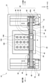
- the mounting device 10 is a device that manufactures a semiconductor device by mounting a plurality of semiconductor chips 100 on a substrate 104 that is a mounted body.
- the mounting device 10 includes a bonding stage 20, a base 21, a mounting head 17, a film arrangement mechanism 30, and a control unit 80 that controls the movement of each of these parts. is doing.
- the extending direction of the cover film 110 will be described as the X direction
- the direction perpendicular to the X direction on the horizontal plane will be described as the Y direction
- the vertical direction will be described as the Z direction.
- the side provided with the take-up roller 63b which will be described later, will be referred to as one side
- the side provided with the delivery roller 63a will be referred to as the other side.
- the bonding stage 20 is a stage that holds the substrate 104 on the upper surface.
- the bonding stage 20 is provided with, for example, a suction hole (not shown) for sucking and holding the substrate 104, a heater for heating the substrate 104 (not shown), and the like.
- the bonding stage 20 is supported by a base 21.
- the mounting head 17 is provided so as to face the bonding stage 20, and includes a main body 11, a heat insulating block 12 mounted on the lower side of the main body 11, a heater 14 mounted on the lower side of the heat insulating block 12, and a heater. It is composed of a pressing tool 16 attached to the lower side of the 14.
- the main body 11 can move in the vertical direction, which is the direction of contact and separation with respect to the substrate 104 adsorbed on the bonding stage 20 by the drive mechanism provided inside, and can also move in the horizontal direction with respect to the substrate 104. It has become.
- the heat insulating block 12 is a ceramic plate-shaped member that is sandwiched between the main body 11 and the heater 14 to prevent the heat of the heater 14 from being transferred to the main body 11.
- the heater 14 is formed by embedding a heat-generating resistor made of platinum, tungsten, or the like inside ceramics such as aluminum nitride.
- the heat insulating block 12 is provided with an air flow path 13 extending in an L shape from the side surface and communicating the side surface and the cooling groove 15 provided in the heater 14.
- the heater 14 When electric power is input from the control unit 80, the heater 14 generates heat and the temperature rises, heating the pressing tool 16 attached to the lower side of the heater 14. Further, when the air from the fan 19 is passed through the air flow path 13 of the heat insulating block 12, the heater 14 is cooled, whereby the pressing tool 16 is cooled.
- the pressing tool 16 has a top surface having substantially the same size as the heater 14, and is provided with a protrusion 16a on the lower side for sucking and pressing the semiconductor chip 100.
- the size of the protrusion 16a is substantially the same as the size of the semiconductor chip 100.
- the pressing tool 16 is made of ceramics.
- the pressing tool 16 is formed with a suction hole 18 for sucking and holding the semiconductor chip 100.
- the suction hole 18 penetrates the heater 14 and the heat insulating block 12 and communicates with a suction pump (not shown) from the main body 11, and the negative pressure generated by the suction pump causes the semiconductor chip 100 to push the protrusion of the pressing tool 16. It is sucked and held on the lower surface of 16a.
- the base 21 of the mounting device 10 is provided with a film arranging mechanism 30 for interposing a cover film 110 between the semiconductor chip 100 and the pressing tool 16 when the semiconductor chip 100 is mounted.
- a material having excellent heat resistance and high peelability of the adhesive material 108 is suitable. Therefore, as the material of the cover film 110, for example, a fluororesin such as polytetrafluoroethylene (PTFE) or tetrafluoroethylene / perfluoroalkyl vinyl ether copolymer (PFA) can be used as the material of the cover film 110.
- PTFE polytetrafluoroethylene
- PFA perfluoroalkyl vinyl ether copolymer
- the film arrangement mechanism 30 includes a film guide 40, a connecting member 46, an elevating mechanism 50, a film feeding mechanism 60, and a moving mechanism 70.
- the film feeding mechanism 60 sequentially feeds the strip-shaped cover film 110 above the substrate 104.
- a feed roller 63a provided on the other side of the bonding stage 20 and a take-up roller 63b provided on one side (hereinafter, when the feed roller 63a / take-up roller 63b are not distinguished, they are simply referred to as "feed roller 63"). have.
- the cover film 110 is hung between the pair of feed rollers 63.
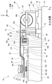
- the feeding roller 63a rotates in a predetermined feeding direction (direction of arrow 91 in FIG. 1), the new cover film 110 is sequentially fed.
- the take-up roller 63b rotates in the same direction as the take-out roller 63a in conjunction with the take-out roller 63a, so that the used cover film 110 is taken up by the take-up roller 63b and collected.
- the delivery roller 63a and the take-up roller 63b are each driven by a drive motor (not shown).
- the delivery roller 63a may be a driven roller that is not driven by a motor and is driven by the rotation of the take-up roller 63b.
- the support structure 65 of the sending roller 63a and the winding roller 63b is the same, and the only difference is that they are symmetrical with respect to the bonding stage 20. Further, the elevating mechanism 50, the film guide 40, and the moving mechanism 70 are provided on one side and the other side of the bonding stage 20, respectively, and both are symmetrical with respect to the bonding stage 20. Only different. Therefore, the support structure 65 of the take-up roller 63b arranged on one side of the bonding stage 20, the elevating mechanism 50, the film guide 40, and the moving mechanism 70 will be described below.
- the support structure 65 of the take-up roller 63b is composed of a base 61 and a frame 62.
- the base 61 is provided on the upper surface of the base 21 on one side of the bonding stage 20 and is mounted on a rail 71 extending in the Y direction so as to be movable in the Y direction.
- the frame 62 is composed of four pillars mounted on the base 61 and four beams connecting the upper portions of the pillars.
- the shaft 64 of the take-up roller 63b is rotatably attached to the two opposing beams extending in the X direction.
- An elevating mechanism 50 is attached to a base 61 that supports the take-up roller 63b of the film feeding mechanism 60, and a film guide 40 is connected to the elevating mechanism 50.
- the film guide 40 defines the height of the cover film 110 with respect to the bonding stage 20, and the elevating mechanism 50 raises and lowers the film guide 40 with respect to the bonding stage 20.
- the elevating mechanism 50 includes a guide rail 51, a slider 54, a connecting member 55, a spring 56, and a Z-direction actuator 58.
- the spring 56 is an example of an elastic member, but the spring 56 is not limited to this, and an elastic member such as a leaf spring, rubber, or sponge can be used.
- the guide rail 51 is attached to the upper surface of the base 61 of the film feeding mechanism 60 so as to extend in the vertical direction.
- the slider 54 is composed of a main body portion 52 and an arm portion 53.
- a hole 52a provided in the center of the main body 52 fits into the guide rail 51 and can move in the vertical direction along the guide rail 51.
- the tip of the Z-direction actuator 58 mounted on the base 61 is connected to the lower end of the main body 52, and the main body 52 is driven in the vertical direction by the Z-direction actuator 58.
- One end of the arm portion 53 is connected to the main body portion 52, the hole 53a provided at the other end is fitted into the slider guide 57 of the connection member 55 described later, and the arm portion 53 can move in the vertical direction with respect to the slider guide 57. It is connected to the.
- the connecting member 55 includes a plate-shaped upper flange 55a, a plate-shaped lower flange 55b facing the upper flange 55a, and a plate-shaped web 55c for connecting the upper flange 55a and the lower flange 55b in the vertical direction. It is a groove-shaped cross-section member.
- a slider guide 57 extending in the vertical direction is provided between the upper flange 55a and the lower flange 55b.
- the hole 53a is fitted into the slider guide 57 and guided by the slider guide 57 so that the arm portion 53 can move vertically with respect to the connecting member 55 between the upper flange 55a and the lower flange 55b. It is connected.
- the arm portion 53 of the slider 54 is attached so as to be relatively movable in the vertical direction with respect to the connecting member 55 by a predetermined vertical width between the lower surface of the upper flange 55a of the connecting member 55 and the upper surface of the lower flange 55b. ..
- the connecting member 55 is attached so as to be relatively movable in the vertical direction with respect to the arm portion 53 of the slider 54 by a predetermined vertical width between the lower surface of the upper flange 55a and the upper surface of the lower flange 55b.
- a spring 56 is attached between the upper surface of the lower flange 55b of the connecting member 55 and the lower surface of the arm portion 53 of the slider 54.
- the spring 56 urges the arm portion 53 upward so that the upper surface of the arm portion 53 of the slider 54 contacts the lower surface of the upper flange 55a.
- the film guide 40 is connected to the surface of the connecting member 55 on the side of the web 55c on the bonding stage 20 side.
- the film guide 40 includes a substrate portion 41, a lower guide roller 42, an upper guide roller 43, and a stopper 44.
- the substrate portion 41 is a longitudinal member connected to the web 55c and extending toward the bonding stage 20 along the side edge of the cover film 110 on the upper surface of the bonding stage 20.
- the lower guide roller 42 is attached to the side surface of the tip end portion of the substrate portion 41 on the bonding stage 20 side, extends from the substrate portion 41 toward the cover film 110 in a direction perpendicular to the extending direction of the cover film 110, and extends downward. It is a cylindrical rotating body around which the cover film 110 is wound.
- the upper guide roller 43 is arranged on one side of the lower guide roller 42.
- the upper guide roller 43 is attached to the side surface of the base portion 41 and extends from the base portion 41 toward the cover film 110 in a direction perpendicular to the extending direction of the cover film 110, and a columnar rotation around which the cover film 110 is wound.
- the body is attached to the side surface of the base portion 41 and extends from the base portion 41 toward the cover film 110 in a direction perpendicular to the extending direction of the cover film 110, and a columnar rotation around which the cover film 110 is wound.
- the stopper 44 is a plate-shaped member attached to the lower end surface of the base portion 41 and extending from the base portion 41 toward the minus side in the Y direction.
- the stopper 44 is arranged at a position where the lower end abuts on the upper surface of one side of the bonding stage 20, and constitutes a contact portion that abuts on the upper surface of the bonding stage 20.
- the height of the stopper 44 is such that when the lower end of the stopper 44 abuts on the upper surface of the bonding stage 20, the height of the lower surface of the cover film 110 contacts the upper surface of the semiconductor chip 100 temporarily crimped onto the substrate 104. It has become.
- the tip of the base portion 41 of the film guide 40 on one side and the tip of the base portion 41 of the film guide 40 on the other side are connected by a connecting member 46.
- the connecting member 46 is a longitudinal member extending in the X direction along the side end of the cover film 110 on the upper surface of the bonding stage 20.
- the film guide 40 on the other side has the same structure as the film guide 40 on the one side except that the film guide 40 has a symmetrical shape with respect to the bonding stage 20.
- the cover film 110 wound around the upper guide roller 43 of the film guide 40 on one side extends toward the take-up roller 63b arranged on one side, and is attached to the take-up roller 63b. It is taken up. Further, the cover film 110 wound around the lower guide roller 42 of the film guide 40 on one side extends to the other side and is wound around the lower side of the lower guide roller 42 of the film guide 40 arranged on the other side. After that, the film guide 40 is wound on the upper side of the upper guide roller 43 arranged on the other side and extends toward the feeding roller 63a.
- the cover film 110 stretched between the feeding roller 63a on the other side and the winding roller 63b on the one side is the lower guide roller 42 of the two film guides 40 arranged on both sides of the bonding stage 20. And the upper guide roller 43, respectively.
- the height of the cover film 110 from the bonding stage 20 is defined by the lower guide rollers 42 on both sides.
- the moving mechanism 70 includes a rail 71 provided on the upper surface of the base 21 on one side of the bonding stage 20, and a film feeding mechanism 60 provided on the base 21 and guided by the rail 71. It is composed of a Y-direction actuator 72 that drives the base 61 of the above in the Y-direction. Since the Y-direction actuator 72 moves the base 61 to which the take-up roller 63b of the film feeding mechanism 60 and the elevating mechanism 50 are connected in the Y direction (direction of arrow 92 in FIG. 2), the film feeding mechanism 60 is wound. The take roller 63b, the elevating mechanism 50, and the film guide 40 connected to the elevating mechanism 50 are integrally moved in the Y direction.
- the support structure 65 of the take-up roller 63b arranged on one side of the bonding stage 20, the elevating mechanism 50, the film guide 40, and the moving mechanism 70 have been described above.
- the support structure 65 of the delivery roller 63a arranged on the other side of the bonding stage 20, the support structure 65 of the take-up roller 63b, the elevating mechanism 50, the film guide 40, and the moving mechanism 70 are attached to the bonding stage 20. Since it has the same structure as one side except that it has a symmetrical shape, the description thereof will be omitted.
- the control unit 80 includes a main body 11 of the mounting head 17, a heater 14, a fan 19, a Z-direction actuator 58 of the elevating mechanism 50, a drive motor (not shown) of the film feeding mechanism 60, and a Y-direction actuator 72 of the moving mechanism 70.
- the control unit 80 includes, for example, a CPU that performs various operations and a memory that stores various data and programs. The detection results of various sensors are input to the control unit 80, and the control unit 80 performs drive control and temperature control of each unit according to the detection results.
- the mounting device 10 mounts the semiconductor chip 100 on the substrate 104 by the flip chip bonder technology. Specifically, as shown in FIG. 1, the mounting device 10 joins a protrusion made of a conductive material called a bump 102 formed on the bottom surface of the semiconductor chip 100 to an electrode 105 formed on the surface of the substrate 104. As a result, the semiconductor chip 100 is electrically connected to the substrate 104.
- the substrate 104 defines a mounting section 106 in which a plurality of electrodes 105 electrically connected to the bump 102 of the semiconductor chip 100 are formed and the semiconductor chip 100 is mounted.
- Each mounting section 106 is previously coated with an adhesive material 108, which is an insulating thermosetting resin.
- the control unit 80 of the mounting device 10 sucks and holds the semiconductor chip 100 on the pressing tool 16 at the tip of the mounting head 17, lowers the mounting head 17, and presses it against the adhesive material 108 of the mounting section 106 to press the adhesive material.
- the semiconductor chip 100 is temporarily crimped onto the 108.
- the cover film 110 is retracted to a position horizontally separated from the mounting section 106 by the moving mechanism 70.
- the control unit 80 drives the moving mechanism 70 to move the cover film 110 in the horizontal direction, and as shown in FIG. 3, the control unit 80 is directly above the temporarily crimped semiconductor chip 100 and is the semiconductor.
- the cover film 110 is moved to a position between the chip 100 and the pressing tool 16.
- the height of the cover film 110 is defined by the lower guide roller 42 of the film guide 40.
- the height of the cover film 110 is between the upper surface of the semiconductor chip 100 and the pressing tool 16.
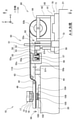
- the control unit 80 operates the Z-direction actuator 58 of the elevating mechanism 50 to lower the main body 52 of the slider 54 as shown by an arrow 93. Then, the arm portion 53 and the film guide 40 also descend as shown by the arrow 94 in FIG. Then, when the slider 54 is lowered by the height ⁇ h1 from the state shown in FIG. 3, the lower end of the stopper 44 of the film guide 40 comes into contact with the bonding stage 20 as shown in FIG. At this time, the lower surface of the cover film 110 has a height in contact with the upper surface of the temporarily crimped semiconductor chip 100.
- control unit 80 further lowers the slider 54 by the height ⁇ h2 by the Z-direction actuator 58.
- the spring 56 is compressed by the height ⁇ h2, and a gap having a height ⁇ h2 is formed between the upper surface of the arm portion 53 of the slider 54 and the lower surface of the upper flange 55a of the connecting member 55.
- the stopper 44 of the film guide 40 is pressed onto the bonding stage 20 by the reaction force due to the compression of the spring 56. This pressing force keeps the height of the film guide 40 with respect to the bonding stage 20 constant.
- the control unit 80 operates the Z-direction actuator 58 of the elevating mechanism 50 arranged on the other side in the same manner as the Z-direction actuator 58 of the elevating mechanism 50 arranged on one side, and presses the stopper 44 of the film guide 40 on the other side. Press against the upper surface of the bonding stage 20.
- the height of the film guide 40 on the other side with respect to the bonding stage 20 becomes the same as the height of the film guide 40 on the other side with respect to the bonding stage 20.
- the parallelism between the cover film 110 and the bonding stage 20 can be ensured. Therefore, as shown in FIG. 2, even when the cover film 110 covers the upper surface of the plurality of semiconductor chips 100 in the longitudinal direction, it can be brought into close contact with the upper surface of each semiconductor chip 100.
- the control unit 80 lowers the mounting head 17 and presses the semiconductor chip 100 from the upper side of the cover film 110 with the protrusion 16a of the pressing tool 16 at the tip.
- the adhesive material 108 protrudes around the semiconductor chip 100, and a part of the adhesive material 108 crawls up the side surface of the semiconductor chip 100 and reaches the lower surface of the cover film 110.
- the bump 102 formed on the semiconductor chip 100 comes into contact with the electrode 105 of the substrate 104.
- the cover film 110 is in close contact with the upper surface of the semiconductor chip 100 and is extruded by the semiconductor chip 100. It is possible to prevent the adhesive material 108 from crawling up unevenly and generating static electricity during mounting.
- the control unit 80 starts supplying electric power to the heater 14, and raises the temperature of the pressing tool 16 by the heater 14.
- the semiconductor chip 100 is heated by the heat and the adhesive material 108 is softened.
- the temperature is further increased to exceed the melting temperature of the bump 102, the bump 102 of the semiconductor chip 100 is melted.
- the adhesive material 108 starts thermal curing.
- control unit 80 starts the fan 19 shown in FIG. 1 and allows cooling air to flow through the air flow path 13 of the heat insulating block 12 to cool the pressing tool 16.
- the molten bump 102 is cured, and the bonding of the substrate 104 with the electrode 105 is completed.
- the temperature of the thermosetting adhesive material 108 also drops, and the mounting is completed in the state shown in FIG.
- the control unit 80 raises the mounting head 17.
- the control unit 80 raises the slider 54 by the Z-direction actuator 58 of the elevating mechanism 50 on one side and the other side.
- the slider 54 rises by the height ⁇ h2 shown in FIG. 6, the upper surface of the arm portion 53 of the slider 54 comes into contact with the lower surface of the upper flange 55a of the connecting member 55.
- the connecting member 55 and the film guide 40 are raised with the rise of the slider 54, and the cover film 110 is also raised accordingly to return to the height shown in FIG.
- the control unit 80 retracts the cover film 110 by the moving mechanism 70 to a position horizontally separated from the next mounting section 106 to which the semiconductor chip 100 is temporarily crimped. Let me.
- the heights of the film guides 40 on both sides are adjusted by the elevating mechanisms 50 arranged on both sides of the bonding stage 20 to form the bonding stage 20 and the cover film 110.
- the parallelism can be ensured, and the cover film 110 can be brought into close contact with the upper surface of the semiconductor chip 100. Therefore, when the semiconductor chip 100 is mounted, it is possible to prevent the adhesive material 108 extruded by the semiconductor chip 100 from crawling up unevenly or generating static electricity during mounting.
- the mounting device 10 of the embodiment since the film guides 40 on both sides are connected by the connecting member 46, the height deviation of the film guides 40 on both sides is eliminated, and the parallelism between the bonding stage 20 and the cover film 110 is eliminated. Can be secured. Further, since the mounting device 10 of the embodiment presses the film guide 40 on the bonding stage 20 by the force of the spring 56, the height of the film guide 40 with respect to the surface of the bonding stage 20 can be made constant, and bonding can be performed. The parallelism between the stage 20 and the cover film 110 can be ensured.
- the film placement mechanism 230 of the mounting device 200 is a film feeding mechanism including a film guide 40 provided on one side, an elevating mechanism 50, a moving mechanism 70, a feeding roller 63a on the other side, and a winding roller 63b on the one side. It is composed of 60, the other side elevating mechanism 350 provided on the other side, and the other side film guide 340. This is because the configuration of the film feeding mechanism 60, the film guide 40 provided on one side, the elevating mechanism 50, and the moving mechanism 70 is the same as that of the mounting device 10 described above with reference to FIGS. 1 to 6. The explanation is omitted.
- the other side elevating mechanism 350 provided on the other side does not include the Z direction actuator 58, the slider 54, and the connecting member 55, and is composed only of the other side guide rail 351.
- the other side guide rail 351 is mounted on the other side base 61 and extends in the vertical direction to guide the other side film guide 340 in the vertical direction.
- the film guide 340 on the other side is connected to the film guide 40 on one side by a connecting member 46, and moves in the vertical direction in accordance with the film guide 40 on the one side.
- the film guide 340 on the other side includes a base portion 341, a lower guide roller 342, an upper guide roller 343, and a stopper 344, similarly to the film guide 40 on the one side.
- the substrate portion 341 has the same structure as the film guide 40 on one side except that a hole for fitting into the guide rail 351 on the other side is provided at the end on the other side and the length in the X direction is long.
- the lower guide roller 342, the upper guide roller 343, and the stopper 344 have the same structure as the lower guide roller 42, the upper guide roller 43, and the stopper 44 on one side, respectively.
- both the film guide 40 on one side and the film guide 340 on the other side are driven up and down by the Z-direction actuator 58 attached to the elevating mechanism 50 on one side, so that the structure is simplified. can do.
- the mounting device 200 can adjust the height of the film guides 40 arranged on both sides of the bonding stage 20 to ensure the parallelism between the bonding stage 20 and the cover film 110.
- the mounting devices 10 and 200 have been described as mounting the semiconductor chip 100 on the substrate 104, but the present invention is not limited to this, and the semiconductor chip 100 can be mounted on another semiconductor chip 100. .. In this case, the other semiconductor chip 100 constitutes an object to be mounted, similarly to the substrate 104.
Landscapes
- Wire Bonding (AREA)
- Die Bonding (AREA)
Abstract
Description
Claims (9)
- 被実装体に配置された半導体チップを押圧する実装装置であって、
前記半導体チップが配置された前記被実装体を保持するボンディングステージと、
前記ボンディングステージを支える基台と、
前記被実装体に対して接離方向に移動して、前記半導体チップを前記被実装体に押圧する押圧ツールが先端に取付けられた実装ヘッドと、
前記基台に設けられ、カバーフィルムを前記ボンディングステージに沿って移動させて前記半導体チップと前記押圧ツールとの間に前記カバーフィルムを配置するフィルム配置機構と、を備え、
前記フィルム配置機構は、
前記カバーフィルムをガイドし、前記ボンディングステージに接触する接触部を有して前記カバーフィルムの前記ボンディングステージに対する高さを規定するフィルムガイドと、
弾性部材を介して前記フィルムガイドに接続され、前記フィルムガイドを前記ボンディングステージに対して昇降させる昇降機構と、を含むこと、
を特徴とする実装装置。 - 請求項1に記載の実装装置であって、
前記フィルムガイドと前記昇降機構とは、前記ボンディングステージを挟んで前記ボンディングステージの両側にそれぞれ設けられていること、
を特徴とする実装装置。 - 請求項2に記載の実装装置であって、
前記フィルム配置機構は、前記ボンディングステージを挟んで前記ボンディングステージの両側にそれぞれ設けられた前記フィルムガイドの間を連結する連結部材を備えること、
を特徴とする実装装置。 - 請求項1から3のいずれか1項に記載の実装装置であって、
前記昇降機構は、
前記基台に設けられて上下方向に延びるガイドレールと、
前記ガイドレールにガイドされて上下方向に移動するスライダと、
一端が前記スライダに対して前記弾性部材を介して所定上下幅だけ上下方向に相対移動可能に取付けられ、他端に前記フィルムガイドが取付けられる接続部材と、を含み、
前記スライダは、前記フィルムガイドの前記接触部が前記ボンディングステージの上面に接した際に、前記弾性部材と前記接続部材とを介して前記フィルムガイドを前記ボンディングステージの上面に押圧すること、
を特徴とする実装装置。 - 請求項4に記載の実装装置であって、
前記フィルム配置機構は、
前記ボンディングステージを挟んで前記ボンディングステージの両側の前記基台に設けられ、前記カバーフィルムが掛け渡される一対のローラを含み、順次、新たな前記カバーフィルムを送りだすフィルム送り出し機構を含み、
前記フィルム送り出し機構は、各前記ローラを支持する各ベースを含み、
前記昇降機構の各前記ガイドレールは各前記ベースに取付けられていること、
を特徴とする実装装置。 - 請求項2に記載の実装装置であって、
前記フィルム配置機構は、
前記ボンディングステージの一方側に設けられた一方側フィルムガイド及び一方側昇降機構と、
前記ボンディングステージの他方側に設けられた他方側フィルムガイド及び他方側昇降機構と、を含み、
前記一方側昇降機構は、
一方側の前記基台に設けられて上下方向に延びる一方側ガイドレールと、
前記一方側ガイドレールにガイドされて上下方向に移動するスライダと、
一端が前記スライダに対して前記弾性部材を介して所定上下幅だけ上下方向に相対移動可能に取付けられ、他端に前記一方側フィルムガイドが取付けられる接続部材と、を含み、
前記他方側昇降機構は、
他方側の前記基台に設けられて上下方向に延びて前記他方側フィルムガイドを上下方向にガイドする他方側ガイドレールを含み、
前記フィルム配置機構は、前記一方側フィルムガイドと前記他方側フィルムガイドとを連結する連結部材を備え、
前記スライダは、前記一方側フィルムガイドの前記接触部と前記他方側フィルムガイドの前記接触部とが前記ボンディングステージの上面に接した際に、前記弾性部材と前記接続部材とを介して前記一方側フィルムガイドの前記接触部を前記ボンディングステージの上面に押圧すると共に、前記連結部材を介して前記他方側フィルムガイドの前記接触部を前記ボンディングステージの上に押圧すること、
を特徴とする実装装置。 - 請求項6に記載の実装装置であって、
前記フィルム配置機構は、
前記ボンディングステージを挟んで前記ボンディングステージの両側の前記基台に設けられ、前記カバーフィルムが掛け渡される一対のローラを含み、順次、新たな前記カバーフィルムを送りだすフィルム送り出し機構を含み、
前記フィルム送り出し機構は、各前記ローラを支持するベースをそれぞれ含み、
前記一方側ガイドレールは一方側の前記ベースに取付けられており、前記他方側ガイドレールは他方側の前記ベースに取付けられていること、
を特徴とする実装装置。 - 請求項4から7のいずれか1項に記載の実装装置であって、
前記接続部材は、上フランジと、前記上フランジと対向する下フランジと、前記上フランジと前記下フランジとの間を接続するウェブとで構成される溝形断面部材で、
前記上フランジと前記下フランジとの間で上下方向に延びるスライダガイドを備え、
前記スライダは、前記スライダガイドにガイドされて前記上フランジと前記下フランジとの間で前記接続部材に対して上下方向に相対移動可能であり、
前記弾性部材は、前記スライダの下端と前記下フランジの上面との間に設けられていること、
を特徴とする実装装置。 - 請求項5または7に記載の実装装置であって、
前記フィルム配置機構は、前記フィルム送り出し機構を前記ボンディングステージに対して水平方向に移動させる移動機構を含むこと、
を特徴とする実装装置。
Priority Applications (5)
| Application Number | Priority Date | Filing Date | Title |
|---|---|---|---|
| US17/642,948 US12191276B2 (en) | 2020-07-16 | 2020-07-16 | Mounting apparatus |
| PCT/JP2020/027600 WO2022013995A1 (ja) | 2020-07-16 | 2020-07-16 | 実装装置 |
| KR1020217041635A KR102619955B1 (ko) | 2020-07-16 | 2020-07-16 | 실장 장치 |
| CN202080042543.3A CN114207796B (zh) | 2020-07-16 | 2020-07-16 | 安装装置 |
| JP2021562898A JP7117805B2 (ja) | 2020-07-16 | 2020-07-16 | 実装装置 |
Applications Claiming Priority (1)
| Application Number | Priority Date | Filing Date | Title |
|---|---|---|---|
| PCT/JP2020/027600 WO2022013995A1 (ja) | 2020-07-16 | 2020-07-16 | 実装装置 |
Publications (1)
| Publication Number | Publication Date |
|---|---|
| WO2022013995A1 true WO2022013995A1 (ja) | 2022-01-20 |
Family
ID=79554526
Family Applications (1)
| Application Number | Title | Priority Date | Filing Date |
|---|---|---|---|
| PCT/JP2020/027600 Ceased WO2022013995A1 (ja) | 2020-07-16 | 2020-07-16 | 実装装置 |
Country Status (5)
| Country | Link |
|---|---|
| US (1) | US12191276B2 (ja) |
| JP (1) | JP7117805B2 (ja) |
| KR (1) | KR102619955B1 (ja) |
| CN (1) | CN114207796B (ja) |
| WO (1) | WO2022013995A1 (ja) |
Families Citing this family (2)
| Publication number | Priority date | Publication date | Assignee | Title |
|---|---|---|---|---|
| KR20230026562A (ko) * | 2021-08-17 | 2023-02-27 | 삼성디스플레이 주식회사 | 본딩 장치 및 그것을 이용한 본딩 방법 |
| CN119347215A (zh) * | 2024-09-03 | 2025-01-24 | 中科光智(重庆)科技有限公司 | 一种纳米银烧结机 |
Citations (4)
| Publication number | Priority date | Publication date | Assignee | Title |
|---|---|---|---|---|
| JP2007012641A (ja) * | 2005-06-28 | 2007-01-18 | Matsushita Electric Ind Co Ltd | 半導体素子実装方法および半導体素子実装装置 |
| JP2009016544A (ja) * | 2007-07-04 | 2009-01-22 | Panasonic Corp | 半導体素子実装装置および実装方法 |
| WO2009128206A1 (ja) * | 2008-04-18 | 2009-10-22 | パナソニック株式会社 | フリップチップ実装方法とフリップチップ実装装置およびそれに使用されるツール保護シート |
| WO2019107395A1 (ja) * | 2017-12-01 | 2019-06-06 | 株式会社新川 | 実装装置 |
Family Cites Families (11)
| Publication number | Priority date | Publication date | Assignee | Title |
|---|---|---|---|---|
| JP2004165536A (ja) | 2002-11-15 | 2004-06-10 | Nippon Avionics Co Ltd | フリップチップ接合方法およびその装置 |
| JP4779945B2 (ja) * | 2006-11-20 | 2011-09-28 | パナソニック株式会社 | シート送り装置及び方法 |
| JP2009111253A (ja) * | 2007-10-31 | 2009-05-21 | Shibaura Mechatronics Corp | 電子部品の実装装置及び実装方法 |
| KR101141795B1 (ko) * | 2010-12-20 | 2012-05-04 | 앰코 테크놀로지 코리아 주식회사 | 반도체 칩 본딩 장치 및 방법 |
| KR101297680B1 (ko) * | 2011-04-22 | 2013-08-21 | 주식회사 테라세미콘 | 풉 지지용 스테이지 및 이를 사용한 웨이퍼 처리 장치 |
| CN104145328A (zh) * | 2012-03-07 | 2014-11-12 | 东丽株式会社 | 半导体装置的制造方法及半导体装置的制造装置 |
| JP2014225602A (ja) * | 2013-05-17 | 2014-12-04 | 芝浦メカトロニクス株式会社 | 電子部品の実装装置及び実装方法 |
| KR101788021B1 (ko) * | 2015-11-12 | 2017-10-23 | 한미반도체 주식회사 | 열압착 본딩장치 |
| CN110709971B (zh) * | 2017-03-28 | 2023-07-25 | 株式会社新川 | 电子零件封装装置 |
| TWI692044B (zh) * | 2017-05-29 | 2020-04-21 | 日商新川股份有限公司 | 封裝裝置以及半導體裝置的製造方法 |
| TWI743726B (zh) * | 2019-04-15 | 2021-10-21 | 日商新川股份有限公司 | 封裝裝置 |
-
2020
- 2020-07-16 KR KR1020217041635A patent/KR102619955B1/ko active Active
- 2020-07-16 JP JP2021562898A patent/JP7117805B2/ja active Active
- 2020-07-16 US US17/642,948 patent/US12191276B2/en active Active
- 2020-07-16 WO PCT/JP2020/027600 patent/WO2022013995A1/ja not_active Ceased
- 2020-07-16 CN CN202080042543.3A patent/CN114207796B/zh active Active
Patent Citations (4)
| Publication number | Priority date | Publication date | Assignee | Title |
|---|---|---|---|---|
| JP2007012641A (ja) * | 2005-06-28 | 2007-01-18 | Matsushita Electric Ind Co Ltd | 半導体素子実装方法および半導体素子実装装置 |
| JP2009016544A (ja) * | 2007-07-04 | 2009-01-22 | Panasonic Corp | 半導体素子実装装置および実装方法 |
| WO2009128206A1 (ja) * | 2008-04-18 | 2009-10-22 | パナソニック株式会社 | フリップチップ実装方法とフリップチップ実装装置およびそれに使用されるツール保護シート |
| WO2019107395A1 (ja) * | 2017-12-01 | 2019-06-06 | 株式会社新川 | 実装装置 |
Also Published As
| Publication number | Publication date |
|---|---|
| JPWO2022013995A1 (ja) | 2022-01-20 |
| CN114207796B (zh) | 2025-02-25 |
| KR20220010771A (ko) | 2022-01-26 |
| US12191276B2 (en) | 2025-01-07 |
| KR102619955B1 (ko) | 2024-01-02 |
| JP7117805B2 (ja) | 2022-08-15 |
| US20220415845A1 (en) | 2022-12-29 |
| CN114207796A (zh) | 2022-03-18 |
Similar Documents
| Publication | Publication Date | Title |
|---|---|---|
| JP6787613B2 (ja) | 実装装置 | |
| KR102117726B1 (ko) | 압착 장치 및 압착 방법 | |
| KR102503964B1 (ko) | 실장 장치 | |
| CN110709971B (zh) | 电子零件封装装置 | |
| JP7117805B2 (ja) | 実装装置 | |
| US12557682B2 (en) | Mounting device comprising semiconductor chip mounted through thermo-compression tool and mounting method thereof | |
| US8921157B2 (en) | Printed substrate manufacturing equipment and manufacturing method | |
| TWI827978B (zh) | 安裝裝置 | |
| TWI655699B (zh) | Electronic component mounting device | |
| TWI791287B (zh) | 封裝裝置以及封裝方法 | |
| KR102284943B1 (ko) | 본딩 장치 및 본딩 방법 | |
| JP4952674B2 (ja) | 基板移送装置 | |
| CN112768396A (zh) | 树脂片固定装置 | |
| JPH05136205A (ja) | ギヤングボンデイング方法および装置 | |
| JP2001332585A (ja) | チップ本圧着方法及びその装置 | |
| KR100375526B1 (ko) | 리드프레임 테이핑설비의 펀칭장치 및 이의 구동방법 | |
| JP2007208106A (ja) | 熱圧着装置及び熱圧着装置に装着される熱圧着ツール、熱圧着装置における熱圧着方法 | |
| JPH03190199A (ja) | アウターリードのボンディングヘッド及びボンディング方法 | |
| JP2010050121A (ja) | 基板搬出装置 | |
| JP2013098504A (ja) | 接続構造体の製造装置及びその製造方法 | |
| JP2010021315A (ja) | 基板移送装置および基板移送方法 | |
| JPH09321069A (ja) | ペレットボンディング方法及び装置 | |
| JPS6235526A (ja) | ボンデイング装置 | |
| JP2001015544A (ja) | ワイヤボンダ |
Legal Events
| Date | Code | Title | Description |
|---|---|---|---|
| ENP | Entry into the national phase |
Ref document number: 2021562898 Country of ref document: JP Kind code of ref document: A |
|
| ENP | Entry into the national phase |
Ref document number: 20217041635 Country of ref document: KR Kind code of ref document: A |
|
| 121 | Ep: the epo has been informed by wipo that ep was designated in this application |
Ref document number: 20944918 Country of ref document: EP Kind code of ref document: A1 |
|
| NENP | Non-entry into the national phase |
Ref country code: DE |
|
| 122 | Ep: pct application non-entry in european phase |
Ref document number: 20944918 Country of ref document: EP Kind code of ref document: A1 |
|
| WWG | Wipo information: grant in national office |
Ref document number: 202080042543.3 Country of ref document: CN |
|
| WWG | Wipo information: grant in national office |
Ref document number: 11202200929Y Country of ref document: SG |
|
| WWP | Wipo information: published in national office |
Ref document number: 11202200929Y Country of ref document: SG |