WO2021260943A1 - スピンコーティング装置 - Google Patents
スピンコーティング装置 Download PDFInfo
- Publication number
- WO2021260943A1 WO2021260943A1 PCT/JP2020/025336 JP2020025336W WO2021260943A1 WO 2021260943 A1 WO2021260943 A1 WO 2021260943A1 JP 2020025336 W JP2020025336 W JP 2020025336W WO 2021260943 A1 WO2021260943 A1 WO 2021260943A1
- Authority
- WO
- WIPO (PCT)
- Prior art keywords
- spin coating
- unit
- coating apparatus
- film
- thickness
- Prior art date
- Legal status (The legal status is an assumption and is not a legal conclusion. Google has not performed a legal analysis and makes no representation as to the accuracy of the status listed.)
- Ceased
Links
Images


Classifications
-
- B—PERFORMING OPERATIONS; TRANSPORTING
- B05—SPRAYING OR ATOMISING IN GENERAL; APPLYING FLUENT MATERIALS TO SURFACES, IN GENERAL
- B05C—APPARATUS FOR APPLYING FLUENT MATERIALS TO SURFACES, IN GENERAL
- B05C11/00—Component parts, details or accessories not specifically provided for in groups B05C1/00 - B05C9/00
- B05C11/02—Apparatus for spreading or distributing liquids or other fluent materials already applied to a surface ; Controlling means therefor; Control of the thickness of a coating by spreading or distributing liquids or other fluent materials already applied to the coated surface
- B05C11/08—Spreading liquid or other fluent material by manipulating the work, e.g. tilting
-
- B—PERFORMING OPERATIONS; TRANSPORTING
- B05—SPRAYING OR ATOMISING IN GENERAL; APPLYING FLUENT MATERIALS TO SURFACES, IN GENERAL
- B05C—APPARATUS FOR APPLYING FLUENT MATERIALS TO SURFACES, IN GENERAL
- B05C11/00—Component parts, details or accessories not specifically provided for in groups B05C1/00 - B05C9/00
- B05C11/10—Storage, supply or control of liquid or other fluent material; Recovery of excess liquid or other fluent material
- B05C11/1002—Means for controlling supply, i.e. flow or pressure, of liquid or other fluent material to the applying apparatus, e.g. valves
- B05C11/1005—Means for controlling supply, i.e. flow or pressure, of liquid or other fluent material to the applying apparatus, e.g. valves responsive to condition of liquid or other fluent material already applied to the surface, e.g. coating thickness, weight or pattern
-
- B—PERFORMING OPERATIONS; TRANSPORTING
- B05—SPRAYING OR ATOMISING IN GENERAL; APPLYING FLUENT MATERIALS TO SURFACES, IN GENERAL
- B05D—PROCESSES FOR APPLYING FLUENT MATERIALS TO SURFACES, IN GENERAL
- B05D1/00—Processes for applying liquids or other fluent materials
- B05D1/40—Distributing applied liquids or other fluent materials by members moving relatively to surface
-
- G—PHYSICS
- G03—PHOTOGRAPHY; CINEMATOGRAPHY; ANALOGOUS TECHNIQUES USING WAVES OTHER THAN OPTICAL WAVES; ELECTROGRAPHY; HOLOGRAPHY
- G03F—PHOTOMECHANICAL PRODUCTION OF TEXTURED OR PATTERNED SURFACES, e.g. FOR PRINTING, FOR PROCESSING OF SEMICONDUCTOR DEVICES; MATERIALS THEREFOR; ORIGINALS THEREFOR; APPARATUS SPECIALLY ADAPTED THEREFOR
- G03F7/00—Photomechanical, e.g. photolithographic, production of textured or patterned surfaces, e.g. printing surfaces; Materials therefor, e.g. comprising photoresists; Apparatus specially adapted therefor
- G03F7/16—Coating processes; Apparatus therefor
-
- H—ELECTRICITY
- H10—SEMICONDUCTOR DEVICES; ELECTRIC SOLID-STATE DEVICES NOT OTHERWISE PROVIDED FOR
- H10P—GENERIC PROCESSES OR APPARATUS FOR THE MANUFACTURE OR TREATMENT OF DEVICES COVERED BY CLASS H10
- H10P72/00—Handling or holding of wafers, substrates or devices during manufacture or treatment thereof
- H10P72/04—Apparatus for manufacture or treatment
- H10P72/0448—Apparatus for applying a liquid, a resin, an ink or the like
-
- H—ELECTRICITY
- H10—SEMICONDUCTOR DEVICES; ELECTRIC SOLID-STATE DEVICES NOT OTHERWISE PROVIDED FOR
- H10P—GENERIC PROCESSES OR APPARATUS FOR THE MANUFACTURE OR TREATMENT OF DEVICES COVERED BY CLASS H10
- H10P72/00—Handling or holding of wafers, substrates or devices during manufacture or treatment thereof
- H10P72/06—Apparatus for monitoring, sorting, marking, testing or measuring
- H10P72/0604—Process monitoring, e.g. flow or thickness monitoring
-
- H—ELECTRICITY
- H10—SEMICONDUCTOR DEVICES; ELECTRIC SOLID-STATE DEVICES NOT OTHERWISE PROVIDED FOR
- H10P—GENERIC PROCESSES OR APPARATUS FOR THE MANUFACTURE OR TREATMENT OF DEVICES COVERED BY CLASS H10
- H10P76/00—Manufacture or treatment of masks on semiconductor bodies, e.g. by lithography or photolithography
-
- B—PERFORMING OPERATIONS; TRANSPORTING
- B05—SPRAYING OR ATOMISING IN GENERAL; APPLYING FLUENT MATERIALS TO SURFACES, IN GENERAL
- B05D—PROCESSES FOR APPLYING FLUENT MATERIALS TO SURFACES, IN GENERAL
- B05D1/00—Processes for applying liquids or other fluent materials
- B05D1/002—Processes for applying liquids or other fluent materials the substrate being rotated
- B05D1/005—Spin coating
-
- G—PHYSICS
- G03—PHOTOGRAPHY; CINEMATOGRAPHY; ANALOGOUS TECHNIQUES USING WAVES OTHER THAN OPTICAL WAVES; ELECTROGRAPHY; HOLOGRAPHY
- G03F—PHOTOMECHANICAL PRODUCTION OF TEXTURED OR PATTERNED SURFACES, e.g. FOR PRINTING, FOR PROCESSING OF SEMICONDUCTOR DEVICES; MATERIALS THEREFOR; ORIGINALS THEREFOR; APPARATUS SPECIALLY ADAPTED THEREFOR
- G03F7/00—Photomechanical, e.g. photolithographic, production of textured or patterned surfaces, e.g. printing surfaces; Materials therefor, e.g. comprising photoresists; Apparatus specially adapted therefor
- G03F7/16—Coating processes; Apparatus therefor
- G03F7/162—Coating on a rotating support, e.g. using a whirler or a spinner
-
- H—ELECTRICITY
- H10—SEMICONDUCTOR DEVICES; ELECTRIC SOLID-STATE DEVICES NOT OTHERWISE PROVIDED FOR
- H10P—GENERIC PROCESSES OR APPARATUS FOR THE MANUFACTURE OR TREATMENT OF DEVICES COVERED BY CLASS H10
- H10P74/00—Testing or measuring during manufacture or treatment of wafers, substrates or devices
- H10P74/20—Testing or measuring during manufacture or treatment of wafers, substrates or devices characterised by the properties tested or measured, e.g. structural or electrical properties
- H10P74/203—Structural properties, e.g. testing or measuring thicknesses, line widths, warpage, bond strengths or physical defects
Definitions
- the present invention relates to a spin coating apparatus, a spin coating method using the spin coating apparatus, and a method for selecting optimum spin coating conditions.
- the spin coating device is one of the typical devices used for applying a resist material to a semiconductor substrate such as a silicon wafer or a mask substrate.
- a substrate is fixed on a rotary table, and a resist material is dropped onto a central portion of the substrate.
- centrifugal force is generated by rotating the turntable to which the substrate is fixed at high speed, and the photoresist is spread from the center to the end of the semiconductor substrate to form a resist layer on the substrate surface.
- Patent Document 1 describes that the variation in film thickness due to the substrate processing temperature is suppressed by adjusting the rotation speed of the substrate in relation to the measurement temperature of the substrate.
- Patent Document 2 describes that the resist material is uniformly applied to the surface of a wafer having a sharp end shape by combining different rotation steps.
- Patent Document 3 describes that the surface of a substrate is coated with a coating liquid, held without being rotated for a certain period of time, and then rotated and spin-coated to suppress variations in film thickness.
- Patent Documents 4, 5 and 6 describe improvements in the structure of the rotary table and its accessories in order to form a more uniform coating film.
- Patent Document 1 Japanese Patent Application Laid-Open No. 2010-40921 Patent Document 2 Japanese Patent Application Laid-Open No. 2012-256780 Patent Document 3 Japanese Patent Application Laid-Open No. 2006-231262 Patent Document 4 Japanese Patent Application Laid-Open No. 2018-202318 Patent Document 5 Japanese Patent Application Laid-Open No. 2016-73240 Patent Document 6 Japanese Patent Application Laid-Open No. 2014-22452 As shown in such an example, the conventional film thickness control is finally formed by adjusting the operating conditions or the structure such as the rotation speed of the spin coating apparatus. The film thickness was close to the ideal state.
- a coating test is performed by adopting some operating condition or structure, the obtained coating film is analyzed, and the analysis result is compared with the target quality to determine whether or not there is a problem with the above operating condition or structure. do. If it is determined that the above operating conditions or structure need to be adjusted, the above operating conditions or structure are reset based on the deviation between the test result and the target value. Then, the coating test is performed again under the reset operating conditions or structure, and the same analysis and judgment are performed.
- the thickness of the coating film being formed or completed is not directly detected during the operation of the spin coating apparatus. Therefore, the operating conditions or structure of the spin coating apparatus at the time of the test cannot be evaluated until after the analysis results of the coating film obtained in the test are accumulated and evaluated. Therefore, the conventional method requires a lot of trial and error until the operating condition or structure of the ideal spin coating apparatus is completed (so-called “conditioning”). In particular, for products such as resist substrates, which have a relatively short life cycle and require mass production, the time and cost required for such "conditioning” are not preferable for market competition.
- the present inventor has studied a means for shortening the period required for setting the above conditions in the manufacture of a resist substrate using a spin coating apparatus.
- a spin coating apparatus having a film thickness measuring unit (1) and an operation adjusting unit (2), wherein the film thickness measuring unit (1) measures the real-time thickness of a film made of a coating liquid by an interferometry method.
- the spin coating apparatus that measures and adjusts the operation of the spin coating apparatus according to the real-time thickness of the film made of the coating liquid.
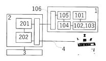
- the film thickness measuring unit (1) has a light source (101), an irradiation unit (102), a light receiving unit (103), a spectroscopic unit (104), and a film thickness calculation unit (105).
- the film thickness measuring unit (1) measures the real-time thickness of a film made of a resist material by an optical interference method
- the rotation control unit (2) measures the real-time thickness of a film made of a resist material.
- the spin coating apparatus of the present invention 1 for applying a resist material onto a substrate which stops the rotation of the spin coating apparatus when the temperature reaches a predetermined range.
- the spin coating device described in the present specification is a device also called a spin coater or a spinner.
- the spin coating apparatus of the present invention has a film thickness measuring unit (1) and an operation adjusting unit (2), which will be described later, and also has all the functions and parts required for a general spin coating apparatus. That is, the spin coating apparatus of the present invention has a rotary table for installing an object to be coated, a nozzle for dropping a coating liquid on the coated object, a rotation mechanism and a circuit for rotating the rotary table, and the above. It is equipped with a control unit for a rotation mechanism.
- the spin coating apparatus of the present invention can be provided with an outer cylinder, a sealing means such as a lid or a locking means, a display unit, and an input unit such as a touch panel or a button, which are attached to the main body.
- the specifications and operating conditions of the main body and its accessories are appropriately designed according to the material and shape (thickness and diameter) of the object to be coated and the properties of the coating liquid.
- the coating liquid applied to the spin coating apparatus of the present invention has an appropriate fluidity capable of spin coating, and the thickness of the film made of the coating liquid can be measured by an interferometry during spin coating. , Not limited.
- Such a coating liquid is, for example, various reactive or non-reactive paints and laminated materials, and is typically a photosensitive material such as a resist material.
- the spin coating apparatus of the present invention has a film thickness measuring unit (1).
- the film thickness measuring unit (1) can measure the thickness of the film made of the coating liquid formed on the surface of the object to be coated by the interferometry regardless of the operating condition (presence or absence of rotation) of the spin coating apparatus of the present invention. can.
- the film thickness measuring unit (1) irradiates the light generated by the light source (101) from the irradiation unit (102) toward the surface of the object to be coated, and the light receiving unit (103) detects the interference light from the surface. do.
- an LED is used as the light source (101), and white light is irradiated from the irradiation unit (102).
- the measurement target is a resist material (resist liquid)
- the wavelength of the light emitted from the irradiation unit (102) is controlled so as to be outside the photosensitive range of the resist material.
- the wavelength of the light emitted from the irradiation unit (102) is controlled to 400 nm or more, preferably 430 nm or more and 700 nm or less, and more preferably 440 nm or more and 700 nm or less.
- the positional relationship between the irradiation unit (102) and the light receiving unit (103) and the rotary table (distance from the reference point such as the center of the substrate, the periphery of the substrate, and the film surface made of the coating liquid) has a high measurement accuracy. As long as it can be secured, it is not limited.
- the detected interference light is sent to the spectroscopic unit (104) and the spectral intensity of the interference light is measured.
- the measured value of the spectral intensity is sent to the film thickness calculation unit (105).
- the film thickness calculation unit (105) uses functions defined by parameters such as light irradiation conditions ( ⁇ : wavelength, ⁇ : incident angle) and optical constants of the coating liquid (n: refractive index, k: extinction coefficient).
- the real-time thickness of the film consisting of the coating liquid is output using the calculated calculation program.
- the measured value consisting of the coating liquid existing on the object to be coated at the time of light irradiation is compared with the theoretical value, and the corrected value of the measured value is output as the real-time thickness of the film made of the coating liquid. ..
- the arithmetic program and the correction method are adopted without limitation from various conventional methods.
- the film thickness measuring unit (1) By continuously irradiating the surface of the object to be coated with light from the irradiation unit (102), the film thickness measuring unit (1) has a film thickness consisting of a coating liquid that changes from moment to moment during the operation of the spin coating apparatus. Can be measured.
- the film thickness measuring unit (1) can output the time-dependent change data of the film thickness from the measured value acquired by the film thickness measuring unit (1) in conjunction with the operation adjusting unit (2) described later.
- the film thickness measuring unit (1) and the operation adjusting unit (2) also function as a monitoring device for the thickness of the film made of the coating liquid.
- the interval of the measurement time can be freely set according to the required accuracy and the coating time.
- the number of measured values output by the film thickness calculation unit (105) per second is set to 1 or more and 20 or less, preferably 2 or more and 10 or less.
- the spin coating device of the present invention has an operation control unit (2).
- the operation control unit (2) is directly incorporated in the control unit included in the main body of the spin coating apparatus of the present invention, or is communication-connected to the control unit included in the main body of the spin coating apparatus.
- the operation adjusting unit (2) receives the real-time thickness of the film made of the coating liquid output by the film thickness measuring unit (1) and stores it in the memory (201).
- the control unit (202) of the film thickness measuring unit (1) compares the real-time thickness of the film composed of the coating liquid stored in the memory (201) with the preset film thickness value (specified thickness). , It is determined whether or not the real-time thickness of the film made of the coating liquid has reached the specified thickness.
- control unit (202) determines that the real-time thickness of the film made of the coating liquid has reached the specified thickness, the control unit (202) generates an operation change command for the spin coating apparatus of the present invention.
- the operation change command is transmitted to the control unit included in the main body of the spin coating apparatus of the present invention.
- the above-mentioned specified thickness is appropriately set according to the target value / ideal value of the thickness of the film made of the coating liquid.
- the operation adjusting unit (2) issues an operation stop command or an operation stop preparation command to the spin coating of the present invention. It is transmitted to the control unit provided in the main body of the device. Then, the rotation of the rotary table of the spin coating apparatus of the present invention is stopped or the mode shifts to the stop preparation mode.
- the spin coating apparatus of the present invention is the same as or different from the display unit attached to the main body of the spin coating apparatus of the present invention, and is a film made of a coating liquid produced by the film thickness measuring unit (1). It can have a display unit (3) for displaying the thickness and the like.
- the user of the spin coating apparatus of the present invention can check the real-time thickness of the film made of the coating liquid displayed on the display unit (3), the change over time of the film made of the coating liquid, the past coating data, the operating condition of the turntable, and the like. , The operation of the spin coating apparatus of the present invention can be observed and monitored.
- the user himself / herself operates the spin coating apparatus of the present invention according to the display on the display unit (3) at the input unit attached to the main body of the spin coating apparatus of the present invention or at an input unit different from the input unit. You can also enter a change command.
- Communication means (4) In the spin coating apparatus of the present invention, the main body and its accessories, the film thickness measuring unit (1), the operation adjusting unit (2), and the display unit (3) are connected to each other. Communication means (4) can be provided.
- the communication means (4) may be adapted to the connected device and is not particularly limited. Generally, short-range communication means such as cable, wireless LAN, Bluetooth (registered trademark), infrared communication, and Near field communication (NFC) are suitable. Further, the spin coating apparatus of the present invention can be connected to the Internet to give operation instructions and observations from an external terminal.
- FIG. 1 shows the relationship between each part in the spin coating apparatus of the present invention.
- FIG. 2 schematically shows the state of light irradiation / detection by the irradiation unit (102) and the light receiving unit (103) of the spin coating apparatus of the present invention.
- FIGS. 1 and 2 some of the actual circuits, connection means, and parts are omitted.
- 1 and 2 are reference views for understanding an example of the arrangement of each part, and do not show the size and shape of the actual device.
- the present invention is not limited to the states shown in FIGS. 1 and 2.
- the spin coating method of the present invention uses the above-mentioned spin coating apparatus.
- the spin coating method of the present invention can acquire the real-time thickness of the film composed of the coating liquid in parallel with the spin coating, and moreover, the operation of the spin coating apparatus based on the thickness acquired during the spin coating. Control can be done.
- Such a spin coating apparatus of the present invention can simultaneously produce and inspect a substrate with a coating film, and spin coating each product according to real-time measured values. Conditions can be adjusted and controlled. Further, since the spin coating apparatus of the present invention can detect a change in the film thickness of the coating liquid with time, it is possible to accurately and easily fit the rotation time and the rotation speed of the rotary table to the target / ideal value.
- the spin coating apparatus of the present invention is particularly effective in selecting the optimum spin coating conditions in test production or pilot production.
- the spin coating apparatus of the present invention is schematically shown.
- the state of light irradiation / detection by the spin coating apparatus of the present invention is schematically shown.
- An example of the spin coating apparatus of the present invention is schematically shown.
- Example 1 Using the spin coating apparatus of the present invention, a film made of a resist material was formed on a substrate.
- FIG. 3 shows the spin coating apparatus used here.
- the nozzle (5) drops 6 ml of the resist material (6) onto the central portion of the substrate.
- the dropped resist material (601) spreads at the end of the substrate by centrifugal force due to the rotation of the rotary table (8) (rotational speed: 3200 rpm) to form a film (602).
- the film thickness measuring unit (1) irradiates the film (602) made of the resist material (6) with light having a wavelength of 400 nm or more and 700 nm or less at equal intervals three times per second.
- the film thickness measuring unit (1) calculates the real-time thickness of the resist material (6) on the substrate from the thickness of the film (602) at the light irradiation point.
- FIG. 3 is a schematic diagram for assisting the understanding of this example, and the actual shape and arrangement of the device are not accurately reproduced.
- the rotary table and a part of the material above it, the member to which the nozzle is connected, some communication connection means, the power supply, and the like are omitted.
- the real-time thickness of the resist material (6) on the substrate output from the film thickness measuring unit (1) is the memory (201) of the PC (2) that functions as the operation adjusting unit (2) together with the data related to other coatings. Accumulate in.
- the PC (2) converts the data accumulated by a predetermined program into display data.
- the desired thickness of the resist material (6) on the substrate is defined as a target value in the operation control unit (2).
- the operation adjusting unit (2) issues a rotary table stop command to the spin coating device. Send.
- the minimum value: 1100 nm and the maximum value: 1250 nm are specified as the target values so that the resist material finally forms a film having a thickness of 1000 nm on the substrate after baking.
- the control unit of the PC (2) compares the real-time thickness of the generated resist material (6) on the substrate with the above target values (minimum value and maximum value), and the resist material (6) on the generated substrate. ) Reached the target range (1100 nm or more and 1250 nm or less), the rotary table (8) was stopped.
- the real-time change in thickness of the resist material (6) on the substrate is displayed according to the display data output by the PC (2).
- the graph shown in FIG. 4 is displayed on the screen (301).
- the vertical axis of the graph of FIG. 4 represents the thickness (nm), and the horizontal axis represents the time (seconds).
- the rotary table (8) started rotating 30 seconds after the start of time measurement. After the start of rotation, the real-time thickness of the resist material (6) on the substrate decreased sharply in about 10 seconds, and reached the target range (1100 nm or more and 1250 nm or less) 70 seconds after the start of time measurement. Sent a rotation stop command to the body of the spin coating device. As a result, the operation of the rotary table (8) was stopped, and the spin coating was completed. From the start to the end of spin coating, the temperature of the spin coating atmosphere (inside the chamber where the rotary table of the spin coating device was placed) and the temperature of the ejection portion of the nozzle were constant at 23 ° C.
- the obtained substrate was dried and heated to obtain a substrate (substrate A1) coated with a film made of a resist material.
- the thickness of the film made of the resist material was measured at a plurality of points on the substrate A1 by an interferometry method.
- Example 2 A new substrate was spin-coated, dried, and heated in the same manner as the substrate A1 to obtain the substrate A2.
- the operation of the rotary table (8) was stopped 72 seconds after the start of the time measurement. From the start to the end of spin coating on the substrate A2, the temperature of the spin coating atmosphere (inside the chamber where the rotary table of the spin coating device was placed) or the temperature of the nozzle ejection part fluctuated from 23 ° C.
- the setting conditions of the thickness measuring unit (1) and the PC (2) were not changed.
- the thickness of the film made of the resist material was measured at a plurality of points on the substrate A2 by an interferometry method.
- the new substrate was spin-coated, dried, and heated in the same manner as the substrate A1 to obtain the substrate A3.
- the operation of the rotary table (8) was stopped 79 seconds after the start of the time measurement. From the start to the end of spin coating on the substrate A3, the temperature of the spin coating atmosphere (inside the chamber where the rotary table of the spin coating device was placed) or the temperature of the nozzle ejection part fluctuated from 23 ° C.
- the setting conditions of the thickness measuring unit (1) and the PC (2) were not changed.
- the thickness of the film made of the resist material was measured at a plurality of points on the substrate A3 by an interferometry method.
- the optimum operating conditions of the spin coating apparatus main body were determined by a conventional method so that the film film made of the final resist material had a thickness of 1000 nm.
- the optimum operating conditions were determined in consideration of the temperature of the spin coating atmosphere.
- Spin coating was performed under the determined optimum operating conditions.
- the obtained substrate was dried and heated under the same conditions as in Examples 1, 2 and 3 to obtain three substrates (substrates B1, B2, B3) coated with a film made of a resist material.
- the thickness of the film made of the resist material was measured by the interferometry under the same conditions as in Examples 1, 2, and 3.
- the stop command of the rotary table by the PC (2) is generated without being affected by the temperature change of the spin coating atmosphere, and the spin coating time is optimally long by the above stop command. It was adjusted to.
- the spin coating apparatus of the present invention a spin coating method using the same, and a method for selecting optimum spin coating conditions bring about simplification of the manufacturing process of various products manufactured by using spin coating.
- the present invention particularly contributes to the reduction of manufacturing cost and the improvement of quality of precision processed products such as resist substrates.
Landscapes
- Physics & Mathematics (AREA)
- General Physics & Mathematics (AREA)
- Exposure Of Semiconductors, Excluding Electron Or Ion Beam Exposure (AREA)
- Coating Apparatus (AREA)
Priority Applications (6)
| Application Number | Priority Date | Filing Date | Title |
|---|---|---|---|
| CN202080102432.7A CN115916420A (zh) | 2020-06-26 | 2020-06-26 | 旋涂装置 |
| PCT/JP2020/025336 WO2021260943A1 (ja) | 2020-06-26 | 2020-06-26 | スピンコーティング装置 |
| EP20942288.0A EP4173725A4 (en) | 2020-06-26 | 2020-06-26 | APPLICATION DEVICE BY CENTRIFUGATION |
| KR1020237002125A KR20230025525A (ko) | 2020-06-26 | 2020-06-26 | 스핀 코팅 장치 |
| JP2022532225A JPWO2021260943A1 (https=) | 2020-06-26 | 2020-06-26 | |
| US18/012,942 US20230266669A1 (en) | 2020-06-26 | 2020-06-26 | Spin-coating device |
Applications Claiming Priority (1)
| Application Number | Priority Date | Filing Date | Title |
|---|---|---|---|
| PCT/JP2020/025336 WO2021260943A1 (ja) | 2020-06-26 | 2020-06-26 | スピンコーティング装置 |
Publications (1)
| Publication Number | Publication Date |
|---|---|
| WO2021260943A1 true WO2021260943A1 (ja) | 2021-12-30 |
Family
ID=79282127
Family Applications (1)
| Application Number | Title | Priority Date | Filing Date |
|---|---|---|---|
| PCT/JP2020/025336 Ceased WO2021260943A1 (ja) | 2020-06-26 | 2020-06-26 | スピンコーティング装置 |
Country Status (6)
| Country | Link |
|---|---|
| US (1) | US20230266669A1 (https=) |
| EP (1) | EP4173725A4 (https=) |
| JP (1) | JPWO2021260943A1 (https=) |
| KR (1) | KR20230025525A (https=) |
| CN (1) | CN115916420A (https=) |
| WO (1) | WO2021260943A1 (https=) |
Families Citing this family (1)
| Publication number | Priority date | Publication date | Assignee | Title |
|---|---|---|---|---|
| CN117637545B (zh) * | 2023-11-30 | 2024-08-23 | 重庆大学 | 一种实验室用半自动化钙钛矿太阳能电池制备方法及其制备系统 |
Citations (8)
| Publication number | Priority date | Publication date | Assignee | Title |
|---|---|---|---|---|
| JPH01278021A (ja) * | 1988-04-29 | 1989-11-08 | Nec Corp | レジストの塗布装置 |
| JPH0265225A (ja) * | 1988-08-31 | 1990-03-05 | General Signal Japan Kk | フォトレジストの塗布方法 |
| JPH02142113A (ja) * | 1988-11-22 | 1990-05-31 | Kawasaki Steel Corp | レジスト塗布装置 |
| JPH02229577A (ja) * | 1989-03-02 | 1990-09-12 | Mitsubishi Electric Corp | 塗布装置 |
| JPH02233176A (ja) * | 1989-03-06 | 1990-09-14 | Mitsubishi Electric Corp | 塗布装置 |
| JPH08236430A (ja) * | 1995-02-27 | 1996-09-13 | Risotetsuku Japan Kk | 膜厚制御方法および装置 |
| JPH10328614A (ja) * | 1997-05-30 | 1998-12-15 | Mitsubishi Chem Corp | 着色レジストの塗布方法 |
| JP2006030070A (ja) * | 2004-07-20 | 2006-02-02 | Opto One Kk | 膜厚検査装置 |
Family Cites Families (8)
| Publication number | Priority date | Publication date | Assignee | Title |
|---|---|---|---|---|
| JP3641162B2 (ja) * | 1998-04-20 | 2005-04-20 | 東京エレクトロン株式会社 | 塗布膜形成装置及びその方法並びにパターン形成方法 |
| JP4342327B2 (ja) * | 2004-01-26 | 2009-10-14 | 住友化学株式会社 | 枚葉塗膜形成方法 |
| JP2006231262A (ja) | 2005-02-28 | 2006-09-07 | Fuji Photo Film Co Ltd | スピンコート製膜法 |
| JP4748192B2 (ja) | 2008-08-07 | 2011-08-17 | 東京エレクトロン株式会社 | 塗布装置、塗布方法、塗布、現像装置及び記憶媒体 |
| JP2012256780A (ja) | 2011-06-10 | 2012-12-27 | Fuji Electric Co Ltd | スピンコート法によるレジスト塗布方法 |
| JP5796555B2 (ja) | 2012-07-13 | 2015-10-21 | トヨタ自動車株式会社 | スピンコート装置 |
| JP6454121B2 (ja) | 2014-10-07 | 2019-01-16 | 積水化学工業株式会社 | スピンコート用シャーレ |
| JP2018202318A (ja) | 2017-06-02 | 2018-12-27 | キヤノン株式会社 | スピンコータ装置、スピンコート方法、ドライフィルムレジストの製造方法および液体吐出ヘッドの製造方法 |
-
2020
- 2020-06-26 CN CN202080102432.7A patent/CN115916420A/zh active Pending
- 2020-06-26 WO PCT/JP2020/025336 patent/WO2021260943A1/ja not_active Ceased
- 2020-06-26 JP JP2022532225A patent/JPWO2021260943A1/ja active Pending
- 2020-06-26 KR KR1020237002125A patent/KR20230025525A/ko not_active Ceased
- 2020-06-26 US US18/012,942 patent/US20230266669A1/en not_active Abandoned
- 2020-06-26 EP EP20942288.0A patent/EP4173725A4/en not_active Withdrawn
Patent Citations (8)
| Publication number | Priority date | Publication date | Assignee | Title |
|---|---|---|---|---|
| JPH01278021A (ja) * | 1988-04-29 | 1989-11-08 | Nec Corp | レジストの塗布装置 |
| JPH0265225A (ja) * | 1988-08-31 | 1990-03-05 | General Signal Japan Kk | フォトレジストの塗布方法 |
| JPH02142113A (ja) * | 1988-11-22 | 1990-05-31 | Kawasaki Steel Corp | レジスト塗布装置 |
| JPH02229577A (ja) * | 1989-03-02 | 1990-09-12 | Mitsubishi Electric Corp | 塗布装置 |
| JPH02233176A (ja) * | 1989-03-06 | 1990-09-14 | Mitsubishi Electric Corp | 塗布装置 |
| JPH08236430A (ja) * | 1995-02-27 | 1996-09-13 | Risotetsuku Japan Kk | 膜厚制御方法および装置 |
| JPH10328614A (ja) * | 1997-05-30 | 1998-12-15 | Mitsubishi Chem Corp | 着色レジストの塗布方法 |
| JP2006030070A (ja) * | 2004-07-20 | 2006-02-02 | Opto One Kk | 膜厚検査装置 |
Non-Patent Citations (1)
| Title |
|---|
| See also references of EP4173725A4 * |
Also Published As
| Publication number | Publication date |
|---|---|
| JPWO2021260943A1 (https=) | 2021-12-30 |
| KR20230025525A (ko) | 2023-02-21 |
| US20230266669A1 (en) | 2023-08-24 |
| EP4173725A4 (en) | 2024-04-24 |
| CN115916420A (zh) | 2023-04-04 |
| EP4173725A1 (en) | 2023-05-03 |
Similar Documents
| Publication | Publication Date | Title |
|---|---|---|
| JP6522915B2 (ja) | 基板上の液体成分の測定方法および基板処理装置 | |
| JP3774094B2 (ja) | 膜厚、加工深さ測定装置及び成膜加工方法 | |
| US10596754B2 (en) | Real time inspection and correction techniques for direct writing systems | |
| KR20020095453A (ko) | 균일한 두께를 위한 도포장치와 막두께 제어방법 | |
| US5618461A (en) | Reflectance method for accurate process calibration in semiconductor wafer heat treatment | |
| TW200932938A (en) | Vacuum coating installation and method of producing a coating layer on a substrate | |
| WO2021260943A1 (ja) | スピンコーティング装置 | |
| CN105336638B (zh) | 一种刻蚀终点检测系统 | |
| EP2972070B1 (en) | Method and system for real-time in-process measurement of coating thickness | |
| JP2020118698A (ja) | 基板上の液体成分の測定方法および基板処理装置 | |
| CN108554669B (zh) | 一种喷嘴、涂布机及涂布方法 | |
| CN108037095B (zh) | 一种黑体绝对发射率的测量装置及方法 | |
| TW202400986A (zh) | 成膜控制裝置、成膜裝置及成膜方法 | |
| CN106876236A (zh) | 监测等离子体工艺制程的装置和方法 | |
| TW201509639A (zh) | 膜或薄膜之製造方法 | |
| KR101547318B1 (ko) | 기판 처리 장치 및 처리 방법과 이를 이용한 레이저 열처리 장치 및 레이저 열처리 방법 | |
| JPWO2021260943A5 (https=) | ||
| KR20170086520A (ko) | 자외선 양생에 대한 공정 감시 | |
| JP3960633B2 (ja) | 膜厚制御方法および装置 | |
| CN104089704B (zh) | 半导体薄膜反应腔辅助温度校准方法 | |
| JPH10206238A (ja) | 塗膜焼き付け温度の測定方法 | |
| JP4920362B2 (ja) | 塗装方法 | |
| TWI830598B (zh) | 溫度檢測裝置及半導體處理裝置 | |
| JP2768720B2 (ja) | 塗布装置 | |
| TWI277090B (en) | Disc manufacturing method and disc manufacturing apparatus |
Legal Events
| Date | Code | Title | Description |
|---|---|---|---|
| 121 | Ep: the epo has been informed by wipo that ep was designated in this application |
Ref document number: 20942288 Country of ref document: EP Kind code of ref document: A1 |
|
| ENP | Entry into the national phase |
Ref document number: 2022532225 Country of ref document: JP Kind code of ref document: A |
|
| ENP | Entry into the national phase |
Ref document number: 20237002125 Country of ref document: KR Kind code of ref document: A |
|
| ENP | Entry into the national phase |
Ref document number: 2020942288 Country of ref document: EP Effective date: 20230126 |
|
| NENP | Non-entry into the national phase |
Ref country code: DE |