WO2021251081A1 - 半導体装置、電子機器 - Google Patents
半導体装置、電子機器 Download PDFInfo
- Publication number
- WO2021251081A1 WO2021251081A1 PCT/JP2021/018899 JP2021018899W WO2021251081A1 WO 2021251081 A1 WO2021251081 A1 WO 2021251081A1 JP 2021018899 W JP2021018899 W JP 2021018899W WO 2021251081 A1 WO2021251081 A1 WO 2021251081A1
- Authority
- WO
- WIPO (PCT)
- Prior art keywords
- semiconductor device
- sub
- power supply
- wiring
- supply line
- Prior art date
- Legal status (The legal status is an assumption and is not a legal conclusion. Google has not performed a legal analysis and makes no representation as to the accuracy of the status listed.)
- Ceased
Links
Images




Classifications
-
- H—ELECTRICITY
- H03—ELECTRONIC CIRCUITRY
- H03F—AMPLIFIERS
- H03F3/00—Amplifiers with only discharge tubes or only semiconductor devices as amplifying elements
- H03F3/45—Differential amplifiers
- H03F3/45071—Differential amplifiers with semiconductor devices only
- H03F3/45076—Differential amplifiers with semiconductor devices only characterised by the way of implementation of the active amplifying circuit in the differential amplifier
- H03F3/45475—Differential amplifiers with semiconductor devices only characterised by the way of implementation of the active amplifying circuit in the differential amplifier using IC blocks as the active amplifying circuit
-
- H—ELECTRICITY
- H10—SEMICONDUCTOR DEVICES; ELECTRIC SOLID-STATE DEVICES NOT OTHERWISE PROVIDED FOR
- H10D—INORGANIC ELECTRIC SEMICONDUCTOR DEVICES
- H10D84/00—Integrated devices formed in or on semiconductor substrates that comprise only semiconducting layers, e.g. on Si wafers or on GaAs-on-Si wafers
- H10D84/60—Integrated devices formed in or on semiconductor substrates that comprise only semiconducting layers, e.g. on Si wafers or on GaAs-on-Si wafers characterised by the integration of at least one component covered by groups H10D10/00 or H10D18/00, e.g. integration of BJTs
- H10D84/645—Combinations of only lateral BJTs
-
- H—ELECTRICITY
- H03—ELECTRONIC CIRCUITRY
- H03F—AMPLIFIERS
- H03F3/00—Amplifiers with only discharge tubes or only semiconductor devices as amplifying elements
- H03F3/45—Differential amplifiers
- H03F3/45071—Differential amplifiers with semiconductor devices only
- H03F3/45076—Differential amplifiers with semiconductor devices only characterised by the way of implementation of the active amplifying circuit in the differential amplifier
- H03F3/4508—Differential amplifiers with semiconductor devices only characterised by the way of implementation of the active amplifying circuit in the differential amplifier using bipolar transistors as the active amplifying circuit
- H03F3/45085—Long tailed pairs
-
- H—ELECTRICITY
- H10—SEMICONDUCTOR DEVICES; ELECTRIC SOLID-STATE DEVICES NOT OTHERWISE PROVIDED FOR
- H10D—INORGANIC ELECTRIC SEMICONDUCTOR DEVICES
- H10D84/00—Integrated devices formed in or on semiconductor substrates that comprise only semiconducting layers, e.g. on Si wafers or on GaAs-on-Si wafers
- H10D84/60—Integrated devices formed in or on semiconductor substrates that comprise only semiconducting layers, e.g. on Si wafers or on GaAs-on-Si wafers characterised by the integration of at least one component covered by groups H10D10/00 or H10D18/00, e.g. integration of BJTs
- H10D84/67—Complementary BJTs
-
- H—ELECTRICITY
- H10—SEMICONDUCTOR DEVICES; ELECTRIC SOLID-STATE DEVICES NOT OTHERWISE PROVIDED FOR
- H10W—GENERIC PACKAGES, INTERCONNECTIONS, CONNECTORS OR OTHER CONSTRUCTIONAL DETAILS OF DEVICES COVERED BY CLASS H10
- H10W20/00—Interconnections in chips, wafers or substrates
- H10W20/40—Interconnections external to wafers or substrates, e.g. back-end-of-line [BEOL] metallisations or vias connecting to gate electrodes
- H10W20/41—Interconnections external to wafers or substrates, e.g. back-end-of-line [BEOL] metallisations or vias connecting to gate electrodes characterised by their conductive parts
- H10W20/427—Power or ground buses
-
- H—ELECTRICITY
- H03—ELECTRONIC CIRCUITRY
- H03F—AMPLIFIERS
- H03F2203/00—Indexing scheme relating to amplifiers with only discharge tubes or only semiconductor devices as amplifying elements covered by H03F3/00
- H03F2203/45—Indexing scheme relating to differential amplifiers
- H03F2203/45528—Indexing scheme relating to differential amplifiers the FBC comprising one or more passive resistors and being coupled between the LC and the IC
-
- H—ELECTRICITY
- H03—ELECTRONIC CIRCUITRY
- H03F—AMPLIFIERS
- H03F2203/00—Indexing scheme relating to amplifiers with only discharge tubes or only semiconductor devices as amplifying elements covered by H03F3/00
- H03F2203/45—Indexing scheme relating to differential amplifiers
- H03F2203/45612—Indexing scheme relating to differential amplifiers the IC comprising one or more input source followers as input stages in the IC
-
- H—ELECTRICITY
- H10—SEMICONDUCTOR DEVICES; ELECTRIC SOLID-STATE DEVICES NOT OTHERWISE PROVIDED FOR
- H10D—INORGANIC ELECTRIC SEMICONDUCTOR DEVICES
- H10D10/00—Bipolar junction transistors [BJT]
- H10D10/40—Vertical BJTs
- H10D10/421—Vertical BJTs having both emitter-base and base-collector junctions ending at the same surface of the body
-
- H—ELECTRICITY
- H10—SEMICONDUCTOR DEVICES; ELECTRIC SOLID-STATE DEVICES NOT OTHERWISE PROVIDED FOR
- H10D—INORGANIC ELECTRIC SEMICONDUCTOR DEVICES
- H10D10/00—Bipolar junction transistors [BJT]
- H10D10/60—Lateral BJTs
-
- H—ELECTRICITY
- H10—SEMICONDUCTOR DEVICES; ELECTRIC SOLID-STATE DEVICES NOT OTHERWISE PROVIDED FOR
- H10D—INORGANIC ELECTRIC SEMICONDUCTOR DEVICES
- H10D84/00—Integrated devices formed in or on semiconductor substrates that comprise only semiconducting layers, e.g. on Si wafers or on GaAs-on-Si wafers
- H10D84/60—Integrated devices formed in or on semiconductor substrates that comprise only semiconducting layers, e.g. on Si wafers or on GaAs-on-Si wafers characterised by the integration of at least one component covered by groups H10D10/00 or H10D18/00, e.g. integration of BJTs
- H10D84/63—Combinations of vertical and lateral BJTs
-
- H—ELECTRICITY
- H10—SEMICONDUCTOR DEVICES; ELECTRIC SOLID-STATE DEVICES NOT OTHERWISE PROVIDED FOR
- H10P—GENERIC PROCESSES OR APPARATUS FOR THE MANUFACTURE OR TREATMENT OF DEVICES COVERED BY CLASS H10
- H10P90/00—Preparation of wafers not covered by a single main group of this subclass, e.g. wafer reinforcement
- H10P90/19—Preparing inhomogeneous wafers
- H10P90/1904—Preparing vertically inhomogeneous wafers
- H10P90/1906—Preparing SOI wafers
-
- H—ELECTRICITY
- H10—SEMICONDUCTOR DEVICES; ELECTRIC SOLID-STATE DEVICES NOT OTHERWISE PROVIDED FOR
- H10W—GENERIC PACKAGES, INTERCONNECTIONS, CONNECTORS OR OTHER CONSTRUCTIONAL DETAILS OF DEVICES COVERED BY CLASS H10
- H10W10/00—Isolation regions in semiconductor bodies between components of integrated devices
- H10W10/10—Isolation regions comprising dielectric materials
- H10W10/181—Semiconductor-on-insulator [SOI] isolation regions, e.g. buried oxide regions of SOI wafers
-
- H—ELECTRICITY
- H10—SEMICONDUCTOR DEVICES; ELECTRIC SOLID-STATE DEVICES NOT OTHERWISE PROVIDED FOR
- H10W—GENERIC PACKAGES, INTERCONNECTIONS, CONNECTORS OR OTHER CONSTRUCTIONAL DETAILS OF DEVICES COVERED BY CLASS H10
- H10W72/00—Interconnections or connectors in packages
- H10W72/50—Bond wires
- H10W72/541—Dispositions of bond wires
- H10W72/5449—Dispositions of bond wires not being orthogonal to a side surface of the chip, e.g. fan-out arrangements
-
- H—ELECTRICITY
- H10—SEMICONDUCTOR DEVICES; ELECTRIC SOLID-STATE DEVICES NOT OTHERWISE PROVIDED FOR
- H10W—GENERIC PACKAGES, INTERCONNECTIONS, CONNECTORS OR OTHER CONSTRUCTIONAL DETAILS OF DEVICES COVERED BY CLASS H10
- H10W72/00—Interconnections or connectors in packages
- H10W72/90—Bond pads, in general
- H10W72/941—Dispositions of bond pads
- H10W72/944—Dispositions of multiple bond pads
- H10W72/9445—Top-view layouts, e.g. mirror arrays
-
- H—ELECTRICITY
- H10—SEMICONDUCTOR DEVICES; ELECTRIC SOLID-STATE DEVICES NOT OTHERWISE PROVIDED FOR
- H10W—GENERIC PACKAGES, INTERCONNECTIONS, CONNECTORS OR OTHER CONSTRUCTIONAL DETAILS OF DEVICES COVERED BY CLASS H10
- H10W90/00—Package configurations
- H10W90/701—Package configurations characterised by the relative positions of pads or connectors relative to package parts
- H10W90/751—Package configurations characterised by the relative positions of pads or connectors relative to package parts of bond wires
Definitions
- the invention disclosed in the present specification relates to a semiconductor device and an electronic device using the same.
- Patent Document 1 As an example of the prior art related to the above, Patent Document 1 can be mentioned.
- the conventional semiconductor device has room for further improvement in its noise characteristics (particularly electromagnetic sensitivity).
- the invention disclosed in the present specification is an object of the present invention to provide a semiconductor device having excellent noise characteristics and an electronic device using the same in view of the above-mentioned problems found by the inventors of the present application.
- the semiconductor device disclosed herein has one or more first subcontacts that are electrically conductive to the substrate, wherein at least one of the first subcontacts is an element on the substrate. It is formed in the arrangement region and has a lower impedance than the substrate.
- FIG. 1 is a diagram showing a comparative example of a semiconductor device.
- FIG. 2 is a diagram showing a first embodiment of a semiconductor device.
- FIG. 3 is a diagram for explaining the basic concept of improving noise characteristics by adjusting impedance.
- FIG. 4 is a diagram showing how a low-pass filter is formed inside an operational amplifier using a resistor.
- FIG. 5 is a diagram showing a second embodiment of the semiconductor device.
- FIG. 6 is a diagram showing a configuration example of an operational amplifier.
- FIG. 7 is a diagram showing a third embodiment of the semiconductor device.
- FIG. 8 is a diagram showing an example of packaging.
- FIG. 9 is a diagram showing an example of the wiring layout.
- FIG. 10 is a diagram schematically showing an ⁇ - ⁇ vertical cross section.
- FIG. 10 is a diagram schematically showing an ⁇ - ⁇ vertical cross section.
- FIG. 11 is a diagram showing a fourth embodiment of the semiconductor device.
- FIG. 12 is a diagram showing a measurement circuit of a radio wave radiation test.
- FIG. 13 is a diagram showing an example of radio wave radiation test results.
- FIG. 14 is a diagram showing the appearance of the vehicle.
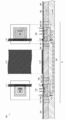
- FIG. 1 is a diagram showing a comparative example of a semiconductor device (upper row: plan view, lower row: vertical cross-sectional view).
- an n-type epi layer 102 having the same crystal plane as the p-type substrate 101 is laminated and formed on the surface of the p-type substrate 101.
- a plurality of circuit elements are formed in the element arrangement region A on the p-type substrate 101, and each circuit element is formed. It is electrically separated by the p-type element separation unit 103.
- the insulating layers 104 and 104x are formed on the surface of the n-type epi layer 102.
- the insulating layer 104x that covers the opening of the circuit element is the insulating layer that covers the other parts. It is formed thinner than 104.
- the transistor 110 is formed of an n-type semiconductor region 111, an n-type semiconductor region 112, a p-type semiconductor region 113, an n-type semiconductor region 114, a p-type semiconductor region 115, and a conductive member 116.
- the n-type semiconductor region 111 is embedded in the boundary surface between the p-type substrate 101 and the n-type epi layer 102.
- a parasitic capacitor Cp is attached between the p-type substrate 101 and the n-type semiconductor region 111.
- the n-type semiconductor region 112 is formed so as to surround a part of the n-type epi layer 102 along the outer peripheral edge of the n-type semiconductor region 111.
- the n-type semiconductor regions 111 and 112 (and the n-type epi layer 102 that conducts with them) correspond to the collector (C) of the transistor 110.
- At least a part of the surface of the n-type semiconductor region 112 is exposed without being covered with the insulating layers 104 and 104x due to electrical conduction with the wiring layer.
- the p-type semiconductor region 113 is formed on the surface of the n-type epi layer 102 surrounded by the n-type semiconductor regions 111 and 112.
- the n-type semiconductor region 114 is formed on the surface of the p-type semiconductor region 113.
- the n-type semiconductor region 114 corresponds to the emitter (E) of the transistor 110, and at least a part of the surface thereof is exposed without being covered with the insulating layers 104 and 104x due to electrical conduction with the wiring layer. There is.
- the p-type semiconductor region 115 is formed on the surface of the p-type semiconductor region 113.
- the p-type semiconductor regions 113 and 115 correspond to the base (B) of the transistor 110, and the p-type semiconductor region 115 has at least a part of the surface insulating layers 104 and 104x due to electrical conduction with the wiring layer. It is exposed without being covered with.
- the conductive member 116 electrically conducts between the wiring L11 and the n-type semiconductor region 112 (collector (C)).
- collector (C) the n-type semiconductor region 112
- the description of the conductive member and the wiring connected to the n-type semiconductor region 114 (emitter (E)) and the p-type semiconductor region 115 (base (B)) is omitted.
- the transistor 120 is formed of an n-type semiconductor region 121, an n-type semiconductor region 122, a p-type semiconductor region 123, a p-type semiconductor region 124, a p-type semiconductor region 125, and a conductive member 126.
- the n-type semiconductor region 121 is embedded in the boundary surface between the p-type substrate 101 and the n-type epi layer 102.
- a parasitic capacitor Cp is attached between the p-type substrate 101 and the n-type semiconductor region 121.
- the n-type semiconductor region 122 is formed so as to surround a part of the n-type epi layer 102 along the outer peripheral edge of the n-type semiconductor region 121.
- the n-type semiconductor regions 121 and 122 (and the n-type epi layer 102 that conducts with them) correspond to the base (B) of the transistor 120, and the n-type semiconductor region 122 is electrically conductive with the wiring layer. Therefore, at least a part of the surface is exposed without being covered with the insulating layers 104 and 104x.
- the p-type semiconductor region 123 is formed so as to be annular in a plan view on the surface of the n-type epi layer 102 surrounded by the n-type semiconductor regions 121 and 122.
- the p-type semiconductor region 124 is formed on the surface of the p-type semiconductor region 123.
- the p-type semiconductor regions 123 and 124 correspond to the collector (C) of the transistor 120, and the p-type semiconductor region 124 has at least a part of the surface of the insulating layers 104 and 104x due to electrical conduction with the wiring layer. It is exposed without being covered with.
- the p-type semiconductor region 125 is formed at a position surrounded by the p-type semiconductor region 124 on the surface of the n-type epi layer 102 surrounded by the n-type semiconductor regions 121 and 122.
- the p-type semiconductor region 125 corresponds to the emitter (E) of the transistor 120, and at least a part of the surface thereof is exposed without being covered with the insulating layers 104 and 104x due to electrical conduction with the wiring layer. There is.
- the conductive member 126 electrically conducts between the wiring L12 and the n-type semiconductor region 122 (base (B)).
- base (B) the n-type semiconductor region 122
- the description of the conductive member and the wiring connected to the p-type semiconductor region 124 (collector (C)) and the p-type semiconductor region 125 (emitter (E)) is omitted. ..
- the distance between the circuit elements (the distance between the transistor 110 and the transistor 120 in this figure) is as large as possible, and the shielding wiring L13 is laid between the two elements to form a semiconductor. It prevented the propagation of noise on the surface (upper layer) of the device 100.
- FIG. 2 is a diagram showing a first embodiment of a semiconductor device (upper row: plan view, lower row: vertical cross-sectional view).
- the semiconductor device 100 of the present embodiment is based on the above-mentioned comparative example (FIG. 1), and is newly provided with a first subcontact 130 and a second subcontact 140.
- the first sub-contact 130 is arranged adjacent to each of the transistors 110 and 120 formed in the element arrangement region A (intervened between the transistors 110 and 120 in this figure).
- the first sub-contact 130 is formed of a p-type semiconductor region 131, a p-type semiconductor region 132, and a conductive member 133 together with the shield wiring L13 described above.
- the p-type semiconductor region 131 penetrates the n-type epi layer 102 in the vertical direction from the surface to the bottom surface, and electrically conducts between the wiring L13 and the p-type substrate 101.
- the p-type semiconductor region 131 does not form a circuit element (excluding parasitic elements) such as a transistor.
- the wiring L13 may be electrically connected to, for example, the ground pad.
- the p-type semiconductor region 131 may be formed by a process common to that of the p-type element separation unit 103.
- the p-type semiconductor region 132 is formed on the surface of the p-type semiconductor region 131. At least a part of the surface of the p-type semiconductor region 132 is exposed without being covered with the insulating layers 104 and 104x due to electrical conduction with the wiring layer.
- the p-type semiconductor region 131 mentioned above has a high impedance because the concentration of p-type impurities is relatively low. Therefore, the impedance is lowered by adding the p-type semiconductor region 132, which has a higher concentration of p-type impurities than the p-type semiconductor region 131. Further, since the p-type semiconductor region 132 is electrically conducted with the wiring L13 via the conductive member 133, low impedance is realized as the first subcontact 130 as a whole.
- the conductive member 133 electrically conducts between the wiring L13 and the p-type semiconductor region 132.
- the wiring L13 has a lower impedance than the p-type substrate 101.
- the surface resistivity of the wiring L13 (for example, Al wiring) is several tens of m ⁇ / sq, while the surface resistivity of the p-type substrate 101 is several hundred ⁇ .
- the noise transmitted from the transistor 110 to the inside (lower layer) of the semiconductor device 100 via the p-type substrate 101 propagates to the first subcontact 130 without reaching the transistor 120, and is finally grounded from the wiring L13. It is escaped toward the pad. Further, the noise transmitted on the surface (upper layer) of the semiconductor device 100 is absorbed by the wiring L13 as in the above-mentioned comparative example (FIG. 1).
- the width W3 of the first subcontact 130 is the minimum process width of the circuit element formed in the element arrangement region A (in this figure, the minimum process width W1 of each of the transistors 110 and 120 and the minimum process width W1. It is desirable to design more than W2).
- the minimum process widths W1 and W2 of the transistors 110 and 120, respectively, are often several tens of ⁇ m (about 50 ⁇ m).
- the width W3 of the first subcontact 130 is 50 ⁇ m or more (preferably 60 ⁇ m or more).
- the width W3 of the first sub-contact 130 is defined as the width of the region sandwiched between the p-type element separating portions 103.
- the width may be defined as the width W3 of the first subcontact 130.
- the second sub-contact 140 is arranged along the outer peripheral edge of the p-type substrate 101, for example, as a GND guard ring surrounding the element arrangement region A.
- the second sub-contact 140 is formed of the p-type semiconductor region 141, the p-type semiconductor region 142, and the conductive member 143 together with the wiring L14.
- the p-type semiconductor region 141 penetrates the n-type epi layer 102 in the vertical direction from the surface to the bottom surface, and electrically conducts between the wiring L14 and the p-type substrate 101.
- the p-type semiconductor region 141 does not form a circuit element (excluding parasitic elements) such as a transistor.
- the wiring L14 may be electrically connected to, for example, the ground pad.
- the p-type semiconductor region 141 may be formed by a process common to the p-type element separation unit 103 and the p-type semiconductor region 131.
- the p-type semiconductor region 142 is formed on the surface of the p-type semiconductor region 141. At least a part of the surface of the p-type semiconductor region 142 is exposed without being covered with the insulating layers 104 and 104x.
- the above-mentioned p-type semiconductor region 141 has a high impedance because the concentration of p-type impurities is relatively low. Therefore, the impedance is lowered by adding the p-type semiconductor region 142, which has a higher concentration of p-type impurities than the p-type semiconductor region 141. Further, since the p-type semiconductor region 142 is electrically conducted with the wiring L14 via the conductive member 143, low impedance is realized as the entire second subcontact 140.
- the conductive member 143 is electrically conductive between the wiring L14 and the p-type semiconductor region 142.
- the wiring L14 has a lower impedance than the p-type substrate 101, like the wiring L13 mentioned above. Therefore, for example, the noise that is about to enter the inside of the chip of the semiconductor device 100 can be absorbed by the second sub-contact 140.
- an operational amplifier (particularly a differential input stage) can be mentioned as one in which noise interference should be avoided. Therefore, in the following, we will consider improving the noise characteristics of the operational amplifier by adjusting the impedance.
- FIG. 3 is a diagram for explaining the basic concept of improving the noise characteristics of the operational amplifier by adjusting the impedance.
- the noise signal input from the outside to the operational amplifier 1 of this configuration example is mainly input to the noise signal N0 input to the power supply terminal VCS and the non-inverting input terminal IN +.
- Examples thereof include a noise signal N1 and a noise signal N2 input to the inverting input terminal IN-due to fluctuation of the output terminal OUT and interference from the noise input line.
- the terminal impedances of the power supply terminal VCS, the non-inverting input terminal IN +, and the inverting input terminal IN- can be raised, so that the input of noise signals N0 to N2 can be suppressed. ..
- FIG. 4 is a diagram showing how a low-pass filter (so-called EMI [electro-magnetic interference] filter) is formed inside the operational amplifier 1 using resistors R0 to R2.
- EMI electro-magnetic interference
- the resistor R0 forms a low-pass filter together with the parasitic capacitor C0 attached to the power supply line of the operational amplifier 1. Further, the resistors R1 and R2 form a low-pass filter together with the parasitic capacitors C1 and C2 attached to the pnp-type bipolar transistors Q1 and Q2 forming the input stage of the operational amplifier 1, respectively.
- the parasitic capacitors C0 to C2 attached to each part thereof are used as the components of the low-pass filter.
- the resistance value R of each of the resistors R1 and R2 may be set based on the following equation (1) from the capacitance value C of each of the parasitic capacitors C1 and C2 and the target cutoff frequency fc of the low-pass filter.
- the resistance value of the resistor R0 may also be basically set based on the above equation (1). However, since the resistor R0 is inserted in the power supply line of the operational amplifier 1, careful attention should be paid to the setting of the resistance value so that the power supply voltage of the operational amplifier 1 does not fall below the drive lower limit voltage thereof. If only a minimum resistor can be used as the resistor R0, the minimum required capacitor may be added separately together with the parasitic capacitor C0.
- FIG. 5 is a diagram showing a second embodiment of the semiconductor device.
- the semiconductor device 100 of this embodiment is a so-called monolithic semiconductor integrated circuit device called an operational capacitor IC, which includes an operational capacitor 1, a reference current setting unit 2, an electrostatic protection element 3 (electrostatic protection diodes D1 and D2), and a power supply.
- the line L1, the grounding line L2, the reference current setting line L3, and the output line L4 are integrated.
- the semiconductor device 100 has a plurality of external terminals (power supply terminal VCS, non-inverting input terminal IN +, inverting input terminal IN-, ground terminal VEE, and ground terminal VEE, as means for establishing an electrical connection with the outside of the device. It is equipped with an output terminal OUT).
- the operational amplifier 1 has resistors R1 and R2 forming a low-pass filter together with parasitic capacitors C1 and C2 (see FIG. 4) (not shown). Specifically, the non-inverting input node (+) of the operational amplifier 1 is connected to the non-inverting input terminal IN + of the semiconductor device 100 via the resistor R1. Further, the inverting input node ( ⁇ ) of the operational amplifier 1 is connected to the inverting input terminal IN ⁇ of the semiconductor device 100 via the resistor R2. In this figure, an example in which the operational amplifier 1 of one channel is integrated in the semiconductor device 100 is given, but the operational amplifier 1 of a plurality of channels may be integrated.
- the reference current setting unit 2 sets the reference current Iref flowing inside the operational amplifier 1.
- the power supply line L1 is laid between the power supply terminal VCC of the semiconductor device 100 and the power supply nodes of the operational amplifier 1 and the reference current setting unit 2.
- the grounding line L2 is laid between the grounding terminal VEE of the semiconductor device 100 and the grounding nodes of the operational amplifier 1 and the reference current setting unit 2.
- the reference current setting line L3 is laid between the reference current setting node of the operational amplifier 1 and the output node of the reference current setting unit 2.
- the output line L4 is laid between the output node of the operational amplifier 1 and the output terminal OUT of the semiconductor device 100.
- the cathode of the electrostatic protection diode D1 is connected to the non-inverting input terminal IN + of the semiconductor device 100.
- the cathode of the electrostatic protection diode D2 is connected to the inverting input terminal IN ⁇ of the semiconductor device 100.
- the anodes of the electrostatic protection diodes D1 and D2 are both connected to the ground terminal VEE of the semiconductor device 100. As described above, if the configuration has the electrostatic protection diodes D1 and D2, it is possible to improve the surge resistance.
- a bypass capacitor for example, 100 pF for stabilizing the power supply voltage is often inserted between the power supply terminal and the ground terminal.
- the bypass capacitor is not connected between the power supply terminal VCS and the ground terminal VEE, and further, the power supply line L1 and the ground line are not connected.
- the parasitic capacitor attached to L2 is also reduced as much as possible (for example, 20 pF or less).
- FIG. 6 is a diagram showing a configuration example of the operational amplifier 1.
- the operational amplifier 1 of this configuration example in addition to the pnp-type bipolar transistors Q1 and Q2 described above, the pnp-type bipolar transistors Q3 to Q6, the npn-type bipolar transistors Q7 to Q13, the resistor R3, the capacitor C3, and the current source are used. Includes I1 to I7.
- the current sources I1 to I7 each flow a reference current Iref (or a constant current corresponding thereto) set by the reference current setting unit 2.
- each of the current sources I1 to I3 are all connected to the power supply terminal VCS.
- the second end of the current source I1 is connected to the emitter of the transistor Q2 and the base of the transistor Q3.
- the second end of the current source I2 is connected to the emitters of the transistors Q3 and Q4, respectively.
- the second end of the current source I3 is connected to the emitter of the transistor Q1 and the base of the transistor Q4.
- the base of the transistor Q1 is connected to the non-inverting input terminal IN + via a resistor R1 (see FIGS. 3 to 5) (not shown).
- the base of the transistor Q2 is connected to the inverting input terminal IN- via a resistor R2 (see FIGS. 3 to 5) (not shown).
- the collectors of the transistors Q1 and Q2 are both connected to the ground terminal VEE.
- the collector of the transistor Q3 is connected to the collector of the transistor Q7.
- the collector of the transistor Q4 is connected to the collector of the transistor Q8.
- the bases of the transistors Q7 and Q8 are both connected to the collector of the transistor Q7.
- the emitters of the transistors Q7 and Q8 are both connected to the ground terminal VEE.
- the current sources I1 to I3, the transistors Q1 to Q4, and the transistors Q7 and Q8 connected in this way form the differential input stage 1X of the operational amplifier 1.
- each of the current sources I4 and I5 are connected to the power supply terminal VCS.
- the second end of the current source I4 is connected to the emitter of the transistor Q5 and the base of the transistor Q9.
- the second end of the current source I5 is connected to the collector of the transistor Q9.
- the base of the transistor Q5 is connected to the collector of the transistor Q8 and the first end of the capacitor C3.
- the second end of the capacitor C3 is connected to the collector of the transistor Q10.
- the emitter of the transistor Q9 is connected to the base of the transistor Q10. Both the collector of the transistor Q5 and the emitter of the transistor Q10 are connected to the ground terminal VEE.
- the first end of the current source I6 and the collectors of the transistors Q12 and Q13 are both connected to the power supply terminal VCC.
- the second end of the current source I6 is connected to the collectors of the transistors Q10 and Q11 and the base of the transistor Q12.
- the emitter of the transistor Q12 is connected to the base of the transistor Q13.
- the emitter of the transistor Q13 is connected to the base of the transistor Q11 and the first end of the resistor R3.
- the emitters of the transistors Q6 and Q11, the second end of the resistor R3, and the first end of the current source I7 are all connected to the output terminal OUT.
- the base of the transistor Q6 is connected to the collector of the transistor Q10. Both the second end of the current source I7 and the collector of the transistor Q6 are connected to the ground terminal VEE.
- the current sources I4 to I7, the transistors Q5 and Q6, the transistors Q9 to Q13, the capacitor C3, and the resistor R3 connected in this way form the amplification output stage 1Y of the operational amplifier 1.
- circuit configuration in this figure is just an example, and any circuit configuration may be adopted as long as the desired operation can be realized as the operational amplifier 1.
- the transistor Q1 forming the differential input stage 1X of the operational amplifier 1 and the transistor Q1 It is advisable to provide the first sub-contact 130 mentioned above so as to be adjacent to Q2. From the opposite point of view, the transistor 110 in FIG. 2 may be understood as the transistors Q1 and Q2. According to such a device structure, it is possible to effectively suppress the noise interference of the operational amplifier 1.
- FIG. 7 is a diagram showing a third embodiment of the semiconductor device.
- SOP Small Outline Package
- SSOP Small SOP
- SOP Small Outline Package
- SOP Small Outline Package
- SSOP Small Outline Package
- SSOP Small Outline Package
- MSOP Micro SOP
- pins 1 to 4 are provided on the first side of the package
- pins 5 to 8 are provided on the second side of the package.
- Pin 1 is the output terminal OUT1 of the first channel and is connected to the output end of the operational amplifier 1a.
- Pin 2 is the inverting input terminal IN1- of the first channel, and is connected to the inverting input terminal (-) of the operational amplifier 1a.
- Pin 3 is the non-inverting input terminal IN1 + of the first channel, and is connected to the non-inverting input terminal (+) of the operational amplifier 1a.
- Pin 4 is a ground terminal VEE.
- Pin 5 is the non-inverting input terminal IN2 + of the second channel, and is connected to the non-inverting input terminal (+) of the operational amplifier 1b.
- Pin 6 is the inverting input terminal IN2- of the second channel, and is connected to the inverting input terminal ( ⁇ ) of the operational amplifier 1b.
- Pin 7 is the output terminal OUT2 of the second channel, and is connected to the output terminal of the operational amplifier 1b.
- Pin 8 is a power supply terminal VCS.
- the external terminals (pins 1 to 3) for the first channel are all provided on the first side of the package, and the external terminals (pins 5 to 7) for the second channel are all provided on the first side of the package. It is provided on the second side of the package.
- FIG. 8 is a diagram showing an example of packaging in the third embodiment.
- the semiconductor chip 300 in which the operational amplifiers 1a and 1b are integrated is sealed with the mold resin 320 in a state of being mounted on the island 310.
- the vertical and horizontal directions of the paper surface are defined as the vertical and horizontal directions in the plan view of the semiconductor device 100 (or the semiconductor chip 300).
- the semiconductor chip 300 has eight pads P1 to P8.
- the pad P1 is a pad corresponding to the output end of the operational amplifier 1a, and is connected to the tip end side of pin 1 (OUT1) via a wire W1.
- the pad P2 is a pad corresponding to the inverting input end ( ⁇ ) of the operational amplifier 1a, and is connected to pin 2 (IN1-) via the wire W2.
- the pad P3 is a pad corresponding to the non-inverting input end (+) of the operational amplifier 1a, and is connected to pin 3 (IN1 +) via the wire W3.
- the pad P4 is a ground pad and is connected to the tip end side of pin 4 (VEE) via a wire W4.
- the pad P5 is a pad corresponding to the non-inverting input end (+) of the operational amplifier 1b, and is connected to pin 5 (IN2 +) via the wire W5.
- the pad P6 is a pad corresponding to the inverting input end ( ⁇ ) of the operational amplifier 1b, and is connected to pin 6 (IN2-) via a wire W6.
- the pad P7 is a pad corresponding to the output end of the operational amplifier 1b, and is connected to the tip end side of pin 7 (OUT7) via a wire W7.
- the pad P8 is a power supply pad and is connected to the tip end side of pin 8 (VCC) via a wire W8.
- the pads P1 to P8 are arranged along the outer peripheral edge of the semiconductor chip 300 in the order corresponding to pins 1 to 8 respectively. Therefore, the laying length of the wires W1 to W8 connecting each pad and each pin can be shortened.
- 1-pin (OUT1), 4-pin (VEE), 5-pin (IN2 +), and 8-pin (VCC) are all 2-pin (IN-) and 3-pin (IN-). It is larger than IN1 +), 6-pin (IN2-), and 7-pin (OUT2).
- pin 1 (OUT1) and pin 4 (VEE) have a portion protruding more than pin 2 (IN1-) and pin 3 (IN1 +).
- pins 5 (IN2 +) and 8 (VCC) have portions that project more than pins 6 (IN2-) and 7 (OUT2).
- pin 1 OUT1
- pin 4 VEE
- pin 5 IN2 +
- pin 8 VCC
- support frames 330 and 340 for supporting the island 310 are formed between the 1-pin (OUT) and the 8-pin (VCC) and between the 4-pin (VEE) and the 5-pin (IN2 +), respectively. ing.
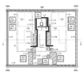
- FIG. 9 is a diagram showing an example of the wiring layout in the third embodiment.
- the vertical and horizontal directions of the paper surface are defined as the vertical and horizontal directions in the plan view of the semiconductor chip 300, and the wiring layout (and pad arrangement) will be described with reference to FIGS. 7 and 8 described above as appropriate.
- the left side of the semiconductor chip 300 in this figure corresponds to the upper side of the semiconductor chip 300 in FIG.
- the right side, the upper side, and the lower side of the semiconductor chip 300 in this figure correspond to the lower side, the right side, and the left side of the semiconductor chip 300 in FIG. 8, respectively. That is, the semiconductor chip 300 in this figure corresponds to a state in which the semiconductor chip 300 in FIG. 8 is rotated counterclockwise by 90 degrees.
- the positions where the pads P1 to P8 are provided correspond to the positions shown in FIG. 8 above.
- the pads P1 (OUT1) and the pads P2 (IN1-) are arranged in the order of the pads P1 and P2 from the upper side to the lower side of the paper surface in the vicinity of the upper left corner 300a of the semiconductor chip 300.
- Pads P3 (IN1 +), pads P4 (VEE), and pads P5 (IN2 +) are arranged in the order of pads P3, P4, and P5 from the left side to the right side of the paper surface in the vicinity of the lower side of the semiconductor chip 300.
- the pad P4 is provided at the center of the lower side of the semiconductor chip 300 in the left-right direction.
- the pads P6 (IN2-) and the pads P7 (OUT2) are arranged in the order of the pads P6 and P7 from the lower side to the upper side of the paper surface in the vicinity of the upper right corner 300d of the semiconductor chip 300.
- the pad P8 (VCC) is provided in the vicinity of the upper side of the semiconductor chip 300, substantially in the center of the upper side in the left-right direction.
- the power supply line L1 is laid from the pad P8 (VCC) while bending or branching toward various circuit elements (for example, the operational amplifiers 1a and 1b and the reference current setting unit 2) formed in the element arrangement region A.
- various circuit elements for example, the operational amplifiers 1a and 1b and the reference current setting unit 2
- FIG. 1 a wiring layout in which two power supply lines L1 extend in the vertical direction of the paper surface is illustrated, but another power supply line L1 extending in the other direction may be laid.
- the element arrangement region A occupies the central portion of the semiconductor chip 300, and is surrounded by the pads P1 to P8. Further, inside the element arrangement area A, from the left side to the right side of the paper surface, the operational amplifier 1a (including the differential input stage 1Xa and the amplification output stage 1Ya), the reference current setting unit 2, the electrostatic protection element 3, and the electrostatic protection element 3 and so on. Each circuit block is formed in the order of the operational amplifier 1b (including the differential input stage 1Xb and the amplified output stage 1Yb). Of course, other circuit blocks may be formed in the element arrangement region A.
- wirings L13a and L13b are laid between the differential input stage 1Xa of the operational amplifier 1a and the reference current setting unit 2, and between the differential input stage 1Xb of the operational amplifier 1b and the reference current setting unit 2, respectively. Has been done. These wirings L13a and L13b form first subcontacts 130a and 130b having lower impedance than the p-type substrate 101, respectively (see also FIG. 10 below).
- the wiring L13 forming the first sub-contact 130 is divided into a plurality of wirings L13a and L13b in addition to the wirings L13a and L13b laid inside the element arrangement area A. That is, the semiconductor chip 300 is formed with a plurality of first sub-contacts 130 that are electrically conductive with the p-type substrate 101, and some of them are arranged inside the element arrangement region A.
- the plurality of wirings L13 are arranged in a flying stone shape from the element arrangement area A to the pad P4 (VEE), and at least one of them is conducted to the pad P4 (VEE). That is, some of the plurality of wirings L13 are directly connected to the pad P4 (VEE), and some are electrically floating.
- the reason why the wiring L13 is divided into a plurality of wirings is that another wiring (for example, a power supply line L1) formed in the same wiring layer is laid in a gap region between the plurality of wirings L13.
- a low impedance noise propagation path can be formed via a series of wirings L13 adjacent to each other in a flying stone shape without hindering the laying of the power supply line L1 and the like.
- the noise propagating inside the element arrangement region A can be absorbed by the wiring L13 and finally released to the pad P4 (VEE), so that the noise characteristics of the operational amplifiers 1a and 1b can be improved.
- VEE pad P4
- the widths of the wirings L13a and L13b to be used are designed to be wider than the widths of the wirings L13 not adjacent to the specific circuit element.
- the wiring L13 (by extension, the first subcontact 130) is located between the differential input stages 1Xa and 1Xb and the power supply line L1, and the amplification output stages 1Ya and 1Yb and the power supply line L1 or the reference. It is desirable to form it between the current setting unit 2 and between the electrostatic protection element 3 and the power supply line L1, respectively.
- the power supply line L1 and the wirings L11 and L12 have a width of several ⁇ m (for example, 2 to 9 ⁇ m).
- the wiring L13 has a width of several tens of ⁇ m (for example, 50 ⁇ m or more).
- the wiring L13 (by extension, the width of the first subcontact 130) has a width of 5 times or more, more preferably 10 times or more, as compared with the power supply line L1 and the wirings L11 and L12.
- the reference current setting unit 2 and the power supply line L1, and the power supply line L1 and the wiring L13 are adjacent to each other.
- the wiring L13 (and by extension, the first sub-contact 130) has a first portion (for example, the differential input stage 1Xa or) in which the distance to the differential input stage 1Xa or 1Xb is shorter than the distance to the amplification output stage 1Ya or 1Yb.
- a portion adjacent to 1Xb) and a second portion (for example, a portion adjacent to the amplification output stage 1Ya or 1Yb) in which the distance to the differential input stage 1Xa or 1Xb is longer than the distance to the amplification output stage 1Ya or 1Yb.
- the width of the first portion is larger than the width of the second portion.
- the power supply line L1 passes through a plurality of wirings L13 (by extension, the first sub-contact 130) and is connected to the differential input stages 1Xa and 1Xb.
- the wiring L13 (by extension, the first sub-contact 130) is arranged so as to vertically or cross the substantially central region of the element arrangement region A in the plan view of the semiconductor chip 300.
- the above-mentioned substantially central region is at least a predetermined length from two sides (left side and right side in this figure) of the element arrangement region A substantially parallel to the laying direction (paper surface vertical direction) of the wiring L13 in the plan view of the semiconductor chip 300. It refers to a region separated by (for example, 1/5 or more of the total length of the upper and lower sides of the element arrangement region A).
- a wiring L14 forming a second sub-contact 140 is laid on the outer peripheral edge of the semiconductor chip 300. Therefore, for example, the noise that is about to enter the inside of the chip of the semiconductor device 100 can be absorbed by the second sub-contact 140.
- the wiring L14 does not necessarily have to be formed in a continuous annular shape, and for example, four wirings L14 formed linearly along each side may be laid. In that case, at the four corners of the semiconductor chip 300, the wirings L14 on each side may be laid out so as to mesh with each other in a plan view (see, for example, the upper left corner 300a, the lower left corner 300b, and the lower right corner 300c of the semiconductor chip 300).
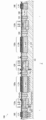
- FIG. 10 is a diagram schematically showing the ⁇ - ⁇ vertical cross section of FIG.
- the device structure of this figure is basically the same as that of the first embodiment (FIG. 2) described above, and as circuit elements forming the operational amplifiers 1a and 1b (particularly, the differential input stages 1Xa and 1Xb), transistors, respectively. 110a and 110b are exemplified. Further, the transistor 120 is exemplified as a circuit element forming the reference current setting unit 2. Corresponding to FIG. 9, wirings L11 and L12 are connected to the transistors 110a and 120, respectively.
- first sub-contacts 130a and 130b are provided between the transistor 110a and the transistor 120 (and the power supply line L1) and between the transistor 110b and the transistor 120 (and the power supply line L1), respectively. ..
- the noise transmitted from the transistor 110a to the inside (lower layer) of the semiconductor device 100 via the p-type substrate 101 propagates to the first subcontact 130a without reaching the transistor 120, and finally is padded from the wiring L13a. It is escaped toward P4 (ground pad). Further, the noise transmitted on the surface (upper layer) of the semiconductor device 100 is absorbed by the wiring L13a as in the above-mentioned comparative example (FIG. 1).
- a second sub-contact 140 is arranged as a GND guard ring surrounding the element arrangement region A. Therefore, the noise that is about to enter the inside of the semiconductor chip 300 can be absorbed by the second sub-contact 140.
- npn-type bipolar transistors 110a and 110b and the pnp-type bipolar transistor 120 are exemplified as the circuit elements formed in the element arrangement region A, but as a matter of course.
- N MOSFETs, P MOSFETs, and other circuit elements may be formed.
- the circuit block for which noise interference is desired differs depending on the application and field of the semiconductor device 100. Therefore, it is important to provide the first sub-contact 130 at an appropriate position.
- FIG. 11 is a diagram showing a fourth embodiment of the semiconductor device. Similar to the second embodiment (FIG. 4), the semiconductor device 100 of the present embodiment has a 1-channel operational amplifier 1 (differential input stage 1X and amplification output stage 1Y (in this figure, amplification stage 1Y1 and output stage 1Y2 are separated). Including)) and the reference current setting unit 2 are integrated.
- the first subcontact 130 (only the wiring L13 is depicted in this figure) may be arranged so as to sandwich both sides (upper and lower in this figure) of the differential input stage 1X of the operational amplifier 1.
- the wiring L13 (by extension, the first sub-contact 130) is located between the differential input stage 1X and the reference current setting unit 2, and the differential input stage 1X and the amplification output stage 1Y (amplification stage 1Y1 and the output stage). It is advisable to place them between 1Y2).
- the power supply line L1 may be installed between the differential input stage 1X and the amplification output stage 1Y.
- the wiring L13 is connected between the differential input stage 1X and the power supply line L1, between the amplification output stage 1Y (amplification stage 1Y1 and the output stage 1Y2), and the power supply line L1. It may be arranged between the output stage 1Y (particularly the output stage 1Y2) and the reference current setting unit 2 or the input pad (IN +, IN-), respectively.
- the second sub-contact 140 along the outer peripheral edge of the semiconductor device 100.
- FIG. 12 is a diagram showing a measurement circuit of a radio wave radiation test in which the semiconductor device 100 is a DUT [device under test].
- the antenna 203, the pseudo power supply 204, the wire harness 250, and the semiconductor device 100 serving as the DUT are all arranged in the anechoic chamber 207.
- a noise signal having a predetermined electric field strength (for example, 200 Vrms) is radiated from the antenna 203 toward the noise injection point of the wire harness 205.
- the total length of the wire harness 205 is 150 cm, and the distance from the noise injection point to the semiconductor device 100 is 75 cm.
- the distance from the antenna 203 to the noise injection point is 100 cm.
- the noise signal is indirectly injected into the power supply terminal VCS of the semiconductor device 100.
- the output voltage appearing at the output terminal OUT (or output terminal OUT1 or OUT2) of the semiconductor device 100 is sequentially read to obtain the frequency vs. You can get a plot of the output voltage.
- FIG. 13 is a diagram schematically showing an example of a radio wave radiation test result.
- the horizontal axis represents the frequency of the noise signal, and the vertical axis represents the output voltage of the semiconductor device 100.
- the solid line is the test result when the semiconductor device 100 of the first to fourth embodiments (see FIGS. 2 to 11) is used as a DUT
- the broken line is the test result when the semiconductor device 100 of the comparative example (FIG. 1) is used as a DUT. It is a test result when it was done.
- the semiconductor device 100 of the first to fourth embodiments can significantly suppress the noise peak over the entire frequency sweep range.
- the semiconductor device 100 of the first to fourth embodiments is very excellent in noise characteristics (particularly electromagnetic sensitivity), and the output fluctuation is extremely small even if noise is input. Therefore, noise countermeasures in the set on which the semiconductor device 100 is mounted are simplified, and the usability is greatly improved.
- FIG. 14 is a diagram showing the appearance of the vehicle.
- the vehicle X in this figure is equipped with various electronic devices X11 to X18 that operate by receiving electric power from a battery.
- Vehicle X includes engine vehicles, electric vehicles (BEV [battery electric vehicle], HEV [hybrid electric vehicle], PHEV / PHV (plug-in hybrid electric vehicle / plug-in hybrid vehicle), or FCEV / FCV.
- BEV battery electric vehicle
- HEV battery electric vehicle
- PHEV / PHV plug-in hybrid electric vehicle / plug-in hybrid vehicle
- FCEV / FCV FCV
- XEV such as fuel cell electric vehicle / fuel cell vehicle
- the electronic device X11 is engine-related control (injection control, electronic throttle control, idling control, oxygen sensor heater control, auto-cruise control, etc.) or motor-related control (torque control, power regeneration control, etc.). It is an electronic control unit that performs.
- the electronic device X12 is a lamp control unit that controls turning on and off such as HID [high intensity discharged lamp] and DRL [daytime running lamp].
- the electronic device X13 is a transmission control unit that performs control related to the transmission.
- the electronic device X14 is a braking unit that performs control related to the movement of the vehicle X (ABS [anti-lock brake system] control, EPS [electric power steering] control, electronic suspension control, etc.).
- ABS anti-lock brake system
- EPS electric power steering
- electronic suspension control etc.
- the electronic device X15 is a security control unit that controls drive such as a door lock and a security alarm.
- the electronic device X16 is an electronic device incorporated in the vehicle X at the factory shipment stage as a standard equipment or a manufacturer's option such as a wiper, an electric door mirror, a power window, a damper (shock absorber), an electric sunroof, and an electric seat. Is.
- the electronic device X17 is an electronic device that is optionally mounted on the vehicle X as a user option such as an in-vehicle A / V [audio / visual] device, a car navigation system, and an ETC [electronic toll collection system].
- the electronic device X18 is an electronic device equipped with a high withstand voltage motor such as an in-vehicle blower, an oil pump, a water pump, and a battery cooling fan.
- a high withstand voltage motor such as an in-vehicle blower, an oil pump, a water pump, and a battery cooling fan.
- the semiconductor device 100 described above can be incorporated into any of the electronic devices X11 to X18.
- the semiconductor device disclosed herein has one or more first subcontacts that are electrically conductive to the substrate, wherein at least one of the first subcontacts is an element on the substrate. It is formed in the arrangement region and has a lower impedance than the substrate (first configuration).
- At least one of the first subcontacts may be configured to be adjacent to the circuit element formed in the element arrangement region (second configuration).
- the second conductive type epi layer is formed on the first conductive type substrate, and the first sub-contact is lower than that of the substrate.
- the configuration (third configuration) may include the first wiring of the impedance and the first conductive type semiconductor region that penetrates the epi layer and conducts the first wiring and the substrate.
- the semiconductor device having the third configuration may have a configuration in which the second wiring is laid between the plurality of first wirings (fourth configuration).
- the width of the first wiring adjacent to the specific circuit element is wider than the width of the first wiring not adjacent to the specific circuit element (in addition, the width of the first wiring is wider than the width of the first wiring not adjacent to the specific circuit element.
- the fifth configuration may be used.
- the specific circuit element may be configured to be a transistor forming a differential input stage (sixth configuration).
- At least one of the first sub-contacts may be configured to be conductive with the ground pad (seventh configuration).
- the width of the first subcontact is equal to or larger than the minimum width of the circuit element formed in the element arrangement region (eighth configuration). It may be.
- the semiconductor device having any of the first to eighth configurations may be configured to further have a second subcontact formed so as to surround the periphery of the element arrangement region (nineth configuration).
- the insulating layer covering the opening of the circuit element formed in the element arrangement region is thinner than the insulating layer covering the other portions. It may be configured (tenth configuration).
- the first subcontact is between the differential input stage of the operational amplifier and the power supply line, and between the amplification output stage of the operational amplifier and the power supply line.
- the configuration (11th configuration) may be provided in at least one of the electrostatic protection element and the power supply line.
- At least a part of the power supply line may be configured to be installed between the differential input stage and the amplification output stage (twelfth configuration). ..
- the width of the first subcontact may be five times or more the width of the power supply line (thirteenth configuration). ..
- the reference current setting unit for setting the reference current of the operational amplifier and the power supply line, and the power supply line and the first subcontact are adjacent to each other. It may be the configuration (14th configuration).
- the first sub-contact has a configuration (15th configuration) installed between the differential input stage and the amplification output stage. You may.
- the first subcontact has a first portion whose distance to the differential input stage is shorter than the distance to the amplification output stage. It has a second portion in which the distance to the differential input stage is longer than the distance to the amplification output stage, and the width of the first portion is larger than the width of the second portion in a plan view.
- the sixth configuration may be used.
- the power supply line passes through between the plurality of first sub-contacts and is connected to the differential input stage (a configuration in which the power supply line is connected to the differential input stage. 17th configuration) may be used.
- the first subcontact has a configuration (18th configuration) in which the first subcontact is arranged in a substantially central region of the element arrangement region in a plan view. You may.
- the first subcontact may have a configuration (19th configuration) that vertically traverses or crosses the substantially central region.
- the electronic device disclosed in the present specification has a configuration (20th configuration) having a semiconductor device having any of the above-mentioned first to nineteenth configurations.
- the operational amplifier used in the in-vehicle device is taken as an example, but the application target is not limited to this, and it is widely and generally applied regardless of the application such as consumer equipment and industrial equipment. It is possible to do.
- the semiconductor device (or operational amplifier) disclosed in the present specification can be used for, for example, an in-vehicle device, a consumer device, or an industrial device.
- Electrostatic protection element 100
- Semiconductor device 101 p-type substrate 102 n-type epi layer 103 p-type element separator 104, 104x Insulation layer 110, 110a, 110b npn-type bipolar transistor 111 n-type semiconductor region 112 n-type semiconductor region 113 p-type semiconductor region 114 n-type semiconductor region 115 p-type semiconductor region 116 conductive member 120 pnp type Bipolar transistor 121 n-type semiconductor region 122 n-type semiconductor region 123 p-type semiconductor region 124 p-type semiconductor region 125 p-type semiconductor region 126
- Conductive member 140 Second sub-contact 141 p-
Landscapes
- Engineering & Computer Science (AREA)
- Power Engineering (AREA)
- Semiconductor Integrated Circuits (AREA)
Priority Applications (4)
| Application Number | Priority Date | Filing Date | Title |
|---|---|---|---|
| CN202180041720.0A CN115702500A (zh) | 2020-06-08 | 2021-05-19 | 半导体器件和电子设备 |
| US17/928,373 US20230223403A1 (en) | 2020-06-08 | 2021-05-19 | Semiconductor device and electronic apparatus |
| DE112021002303.9T DE112021002303B4 (de) | 2020-06-08 | 2021-05-19 | Halbleiterbauelement |
| JP2022530087A JP7731879B2 (ja) | 2020-06-08 | 2021-05-19 | 半導体装置、電子機器 |
Applications Claiming Priority (2)
| Application Number | Priority Date | Filing Date | Title |
|---|---|---|---|
| JP2020-099164 | 2020-06-08 | ||
| JP2020099164 | 2020-06-08 |
Publications (1)
| Publication Number | Publication Date |
|---|---|
| WO2021251081A1 true WO2021251081A1 (ja) | 2021-12-16 |
Family
ID=78847227
Family Applications (1)
| Application Number | Title | Priority Date | Filing Date |
|---|---|---|---|
| PCT/JP2021/018899 Ceased WO2021251081A1 (ja) | 2020-06-08 | 2021-05-19 | 半導体装置、電子機器 |
Country Status (5)
| Country | Link |
|---|---|
| US (1) | US20230223403A1 (https=) |
| JP (1) | JP7731879B2 (https=) |
| CN (1) | CN115702500A (https=) |
| DE (1) | DE112021002303B4 (https=) |
| WO (1) | WO2021251081A1 (https=) |
Citations (10)
| Publication number | Priority date | Publication date | Assignee | Title |
|---|---|---|---|---|
| JPH08115985A (ja) * | 1994-10-17 | 1996-05-07 | Nec Corp | 低雑音の半導体集積回路 |
| JP2000114461A (ja) * | 1998-09-29 | 2000-04-21 | Sanyo Electric Co Ltd | 半導体集積回路装置 |
| JP2002246553A (ja) * | 2001-02-16 | 2002-08-30 | Matsushita Electric Ind Co Ltd | 半導体集積回路のノイズ低減装置 |
| JP2005039320A (ja) * | 2003-07-15 | 2005-02-10 | Renesas Technology Corp | 半導体素子及び高周波電力増幅装置 |
| JP2008071818A (ja) * | 2006-09-12 | 2008-03-27 | Nec Electronics Corp | 半導体装置 |
| JP2008112857A (ja) * | 2006-10-30 | 2008-05-15 | Nec Electronics Corp | 半導体集積回路装置 |
| JP2008193019A (ja) * | 2007-02-08 | 2008-08-21 | Matsushita Electric Ind Co Ltd | 半導体集積回路装置 |
| JP2012009841A (ja) * | 2010-05-21 | 2012-01-12 | Semiconductor Energy Lab Co Ltd | 半導体素子、及び半導体装置 |
| WO2019039245A1 (ja) * | 2017-08-22 | 2019-02-28 | ローム株式会社 | オペアンプ |
| JP2020004935A (ja) * | 2018-07-02 | 2020-01-09 | Tianma Japan株式会社 | イメージセンサ |
Family Cites Families (4)
| Publication number | Priority date | Publication date | Assignee | Title |
|---|---|---|---|---|
| JP4513575B2 (ja) * | 2005-01-12 | 2010-07-28 | 三菱電機株式会社 | 保持解放機構 |
| JP5724934B2 (ja) | 2011-07-05 | 2015-05-27 | 株式会社デンソー | 半導体装置 |
| US10608168B2 (en) * | 2017-10-04 | 2020-03-31 | Allegro Microsystems, Llc | Isolated hall effect element with improved electro-magnetic isolation |
| JP2020004936A (ja) * | 2018-07-02 | 2020-01-09 | 株式会社デンソー | 半導体装置およびその製造方法 |
-
2021
- 2021-05-19 US US17/928,373 patent/US20230223403A1/en active Pending
- 2021-05-19 JP JP2022530087A patent/JP7731879B2/ja active Active
- 2021-05-19 DE DE112021002303.9T patent/DE112021002303B4/de active Active
- 2021-05-19 WO PCT/JP2021/018899 patent/WO2021251081A1/ja not_active Ceased
- 2021-05-19 CN CN202180041720.0A patent/CN115702500A/zh active Pending
Patent Citations (10)
| Publication number | Priority date | Publication date | Assignee | Title |
|---|---|---|---|---|
| JPH08115985A (ja) * | 1994-10-17 | 1996-05-07 | Nec Corp | 低雑音の半導体集積回路 |
| JP2000114461A (ja) * | 1998-09-29 | 2000-04-21 | Sanyo Electric Co Ltd | 半導体集積回路装置 |
| JP2002246553A (ja) * | 2001-02-16 | 2002-08-30 | Matsushita Electric Ind Co Ltd | 半導体集積回路のノイズ低減装置 |
| JP2005039320A (ja) * | 2003-07-15 | 2005-02-10 | Renesas Technology Corp | 半導体素子及び高周波電力増幅装置 |
| JP2008071818A (ja) * | 2006-09-12 | 2008-03-27 | Nec Electronics Corp | 半導体装置 |
| JP2008112857A (ja) * | 2006-10-30 | 2008-05-15 | Nec Electronics Corp | 半導体集積回路装置 |
| JP2008193019A (ja) * | 2007-02-08 | 2008-08-21 | Matsushita Electric Ind Co Ltd | 半導体集積回路装置 |
| JP2012009841A (ja) * | 2010-05-21 | 2012-01-12 | Semiconductor Energy Lab Co Ltd | 半導体素子、及び半導体装置 |
| WO2019039245A1 (ja) * | 2017-08-22 | 2019-02-28 | ローム株式会社 | オペアンプ |
| JP2020004935A (ja) * | 2018-07-02 | 2020-01-09 | Tianma Japan株式会社 | イメージセンサ |
Also Published As
| Publication number | Publication date |
|---|---|
| DE112021002303T5 (de) | 2023-03-16 |
| CN115702500A (zh) | 2023-02-14 |
| US20230223403A1 (en) | 2023-07-13 |
| JPWO2021251081A1 (https=) | 2021-12-16 |
| DE112021002303B4 (de) | 2023-09-21 |
| JP7731879B2 (ja) | 2025-09-01 |
Similar Documents
| Publication | Publication Date | Title |
|---|---|---|
| US11528001B2 (en) | Operational amplifier | |
| CN110021595B (zh) | 半导体装置 | |
| US10027250B2 (en) | Semiconductor device with power elements and current detection portion | |
| US20070034980A1 (en) | Photodiode and phototransistor | |
| WO2021251081A1 (ja) | 半導体装置、電子機器 | |
| JP2751650B2 (ja) | 半導体回路 | |
| GB2120843A (en) | Semiconductor integrated circuit device | |
| US5160997A (en) | Semiconductor integrated circuit with shield electrodes for protecting the interconnection lines from undesirable radiation | |
| JP4381592B2 (ja) | 半導体装置 | |
| CN103890931A (zh) | 半导体装置及半导体模块 | |
| US7339249B2 (en) | Semiconductor device | |
| CN111725207A (zh) | 半导体装置以及放大器模块 | |
| US20230215811A1 (en) | Multi-channel gate driver package with grounded shield metal | |
| JPH0955471A (ja) | サージ保護回路 | |
| CN209911942U (zh) | 触控膜、触控模组及触摸屏 | |
| TW201432829A (zh) | 半導體積體電路 | |
| CN111278265A (zh) | 具有隔离屏蔽结构的信号走线 | |
| JP2793455B2 (ja) | 高周波用ic | |
| JPH08316330A (ja) | 半導体集積回路のレイアウト方法 | |
| JPH0251253A (ja) | 半導体集積回路 | |
| JPS58143565A (ja) | 半導体回路配線体 | |
| JPH07326935A (ja) | 半導体集積回路装置 | |
| JP2021052159A (ja) | 半導体装置及び増幅器モジュール | |
| CN112703593A (zh) | 布线基板 | |
| JP2000040795A (ja) | 半導体集積回路装置および基準電圧配線のレイアウト方法 |
Legal Events
| Date | Code | Title | Description |
|---|---|---|---|
| 121 | Ep: the epo has been informed by wipo that ep was designated in this application |
Ref document number: 21823117 Country of ref document: EP Kind code of ref document: A1 |
|
| ENP | Entry into the national phase |
Ref document number: 2022530087 Country of ref document: JP Kind code of ref document: A |
|
| 122 | Ep: pct application non-entry in european phase |
Ref document number: 21823117 Country of ref document: EP Kind code of ref document: A1 |