WO2021241447A1 - Dispositif à semi-conducteur et procédé de fabrication de dispositif à semi-conducteur - Google Patents
Dispositif à semi-conducteur et procédé de fabrication de dispositif à semi-conducteur Download PDFInfo
- Publication number
- WO2021241447A1 WO2021241447A1 PCT/JP2021/019392 JP2021019392W WO2021241447A1 WO 2021241447 A1 WO2021241447 A1 WO 2021241447A1 JP 2021019392 W JP2021019392 W JP 2021019392W WO 2021241447 A1 WO2021241447 A1 WO 2021241447A1
- Authority
- WO
- WIPO (PCT)
- Prior art keywords
- insulating layer
- layer
- semiconductor device
- main
- thickness direction
- Prior art date
Links
Images


Classifications
-
- H—ELECTRICITY
- H01—ELECTRIC ELEMENTS
- H01L—SEMICONDUCTOR DEVICES NOT COVERED BY CLASS H10
- H01L23/00—Details of semiconductor or other solid state devices
- H01L23/48—Arrangements for conducting electric current to or from the solid state body in operation, e.g. leads, terminal arrangements ; Selection of materials therefor
- H01L23/488—Arrangements for conducting electric current to or from the solid state body in operation, e.g. leads, terminal arrangements ; Selection of materials therefor consisting of soldered or bonded constructions
- H01L23/498—Leads, i.e. metallisations or lead-frames on insulating substrates, e.g. chip carriers
- H01L23/49811—Additional leads joined to the metallisation on the insulating substrate, e.g. pins, bumps, wires, flat leads
- H01L23/49816—Spherical bumps on the substrate for external connection, e.g. ball grid arrays [BGA]
-
- H—ELECTRICITY
- H01—ELECTRIC ELEMENTS
- H01L—SEMICONDUCTOR DEVICES NOT COVERED BY CLASS H10
- H01L23/00—Details of semiconductor or other solid state devices
- H01L23/28—Encapsulations, e.g. encapsulating layers, coatings, e.g. for protection
- H01L23/29—Encapsulations, e.g. encapsulating layers, coatings, e.g. for protection characterised by the material, e.g. carbon
- H01L23/293—Organic, e.g. plastic
-
- H—ELECTRICITY
- H01—ELECTRIC ELEMENTS
- H01L—SEMICONDUCTOR DEVICES NOT COVERED BY CLASS H10
- H01L24/00—Arrangements for connecting or disconnecting semiconductor or solid-state bodies; Methods or apparatus related thereto
- H01L24/01—Means for bonding being attached to, or being formed on, the surface to be connected, e.g. chip-to-package, die-attach, "first-level" interconnects; Manufacturing methods related thereto
- H01L24/02—Bonding areas ; Manufacturing methods related thereto
- H01L24/04—Structure, shape, material or disposition of the bonding areas prior to the connecting process
- H01L24/05—Structure, shape, material or disposition of the bonding areas prior to the connecting process of an individual bonding area
-
- H—ELECTRICITY
- H01—ELECTRIC ELEMENTS
- H01L—SEMICONDUCTOR DEVICES NOT COVERED BY CLASS H10
- H01L24/00—Arrangements for connecting or disconnecting semiconductor or solid-state bodies; Methods or apparatus related thereto
- H01L24/01—Means for bonding being attached to, or being formed on, the surface to be connected, e.g. chip-to-package, die-attach, "first-level" interconnects; Manufacturing methods related thereto
- H01L24/10—Bump connectors ; Manufacturing methods related thereto
- H01L24/15—Structure, shape, material or disposition of the bump connectors after the connecting process
- H01L24/16—Structure, shape, material or disposition of the bump connectors after the connecting process of an individual bump connector
-
- H—ELECTRICITY
- H01—ELECTRIC ELEMENTS
- H01L—SEMICONDUCTOR DEVICES NOT COVERED BY CLASS H10
- H01L24/00—Arrangements for connecting or disconnecting semiconductor or solid-state bodies; Methods or apparatus related thereto
- H01L24/01—Means for bonding being attached to, or being formed on, the surface to be connected, e.g. chip-to-package, die-attach, "first-level" interconnects; Manufacturing methods related thereto
- H01L24/42—Wire connectors; Manufacturing methods related thereto
- H01L24/47—Structure, shape, material or disposition of the wire connectors after the connecting process
- H01L24/48—Structure, shape, material or disposition of the wire connectors after the connecting process of an individual wire connector
-
- H—ELECTRICITY
- H01—ELECTRIC ELEMENTS
- H01L—SEMICONDUCTOR DEVICES NOT COVERED BY CLASS H10
- H01L24/00—Arrangements for connecting or disconnecting semiconductor or solid-state bodies; Methods or apparatus related thereto
- H01L24/73—Means for bonding being of different types provided for in two or more of groups H01L24/10, H01L24/18, H01L24/26, H01L24/34, H01L24/42, H01L24/50, H01L24/63, H01L24/71
-
- H—ELECTRICITY
- H01—ELECTRIC ELEMENTS
- H01L—SEMICONDUCTOR DEVICES NOT COVERED BY CLASS H10
- H01L2224/00—Indexing scheme for arrangements for connecting or disconnecting semiconductor or solid-state bodies and methods related thereto as covered by H01L24/00
- H01L2224/01—Means for bonding being attached to, or being formed on, the surface to be connected, e.g. chip-to-package, die-attach, "first-level" interconnects; Manufacturing methods related thereto
- H01L2224/02—Bonding areas; Manufacturing methods related thereto
- H01L2224/04—Structure, shape, material or disposition of the bonding areas prior to the connecting process
- H01L2224/04042—Bonding areas specifically adapted for wire connectors, e.g. wirebond pads
-
- H—ELECTRICITY
- H01—ELECTRIC ELEMENTS
- H01L—SEMICONDUCTOR DEVICES NOT COVERED BY CLASS H10
- H01L2224/00—Indexing scheme for arrangements for connecting or disconnecting semiconductor or solid-state bodies and methods related thereto as covered by H01L24/00
- H01L2224/01—Means for bonding being attached to, or being formed on, the surface to be connected, e.g. chip-to-package, die-attach, "first-level" interconnects; Manufacturing methods related thereto
- H01L2224/10—Bump connectors; Manufacturing methods related thereto
- H01L2224/15—Structure, shape, material or disposition of the bump connectors after the connecting process
- H01L2224/16—Structure, shape, material or disposition of the bump connectors after the connecting process of an individual bump connector
- H01L2224/161—Disposition
- H01L2224/16151—Disposition the bump connector connecting between a semiconductor or solid-state body and an item not being a semiconductor or solid-state body, e.g. chip-to-substrate, chip-to-passive
- H01L2224/16221—Disposition the bump connector connecting between a semiconductor or solid-state body and an item not being a semiconductor or solid-state body, e.g. chip-to-substrate, chip-to-passive the body and the item being stacked
- H01L2224/16225—Disposition the bump connector connecting between a semiconductor or solid-state body and an item not being a semiconductor or solid-state body, e.g. chip-to-substrate, chip-to-passive the body and the item being stacked the item being non-metallic, e.g. insulating substrate with or without metallisation
-
- H—ELECTRICITY
- H01—ELECTRIC ELEMENTS
- H01L—SEMICONDUCTOR DEVICES NOT COVERED BY CLASS H10
- H01L2224/00—Indexing scheme for arrangements for connecting or disconnecting semiconductor or solid-state bodies and methods related thereto as covered by H01L24/00
- H01L2224/01—Means for bonding being attached to, or being formed on, the surface to be connected, e.g. chip-to-package, die-attach, "first-level" interconnects; Manufacturing methods related thereto
- H01L2224/42—Wire connectors; Manufacturing methods related thereto
- H01L2224/47—Structure, shape, material or disposition of the wire connectors after the connecting process
- H01L2224/48—Structure, shape, material or disposition of the wire connectors after the connecting process of an individual wire connector
- H01L2224/481—Disposition
- H01L2224/48151—Connecting between a semiconductor or solid-state body and an item not being a semiconductor or solid-state body, e.g. chip-to-substrate, chip-to-passive
-
- H—ELECTRICITY
- H01—ELECTRIC ELEMENTS
- H01L—SEMICONDUCTOR DEVICES NOT COVERED BY CLASS H10
- H01L2224/00—Indexing scheme for arrangements for connecting or disconnecting semiconductor or solid-state bodies and methods related thereto as covered by H01L24/00
- H01L2224/73—Means for bonding being of different types provided for in two or more of groups H01L2224/10, H01L2224/18, H01L2224/26, H01L2224/34, H01L2224/42, H01L2224/50, H01L2224/63, H01L2224/71
- H01L2224/732—Location after the connecting process
- H01L2224/73251—Location after the connecting process on different surfaces
- H01L2224/73265—Layer and wire connectors
-
- H—ELECTRICITY
- H01—ELECTRIC ELEMENTS
- H01L—SEMICONDUCTOR DEVICES NOT COVERED BY CLASS H10
- H01L23/00—Details of semiconductor or other solid state devices
- H01L23/28—Encapsulations, e.g. encapsulating layers, coatings, e.g. for protection
- H01L23/31—Encapsulations, e.g. encapsulating layers, coatings, e.g. for protection characterised by the arrangement or shape
- H01L23/3107—Encapsulations, e.g. encapsulating layers, coatings, e.g. for protection characterised by the arrangement or shape the device being completely enclosed
- H01L23/3121—Encapsulations, e.g. encapsulating layers, coatings, e.g. for protection characterised by the arrangement or shape the device being completely enclosed a substrate forming part of the encapsulation
- H01L23/3128—Encapsulations, e.g. encapsulating layers, coatings, e.g. for protection characterised by the arrangement or shape the device being completely enclosed a substrate forming part of the encapsulation the substrate having spherical bumps for external connection
-
- H—ELECTRICITY
- H01—ELECTRIC ELEMENTS
- H01L—SEMICONDUCTOR DEVICES NOT COVERED BY CLASS H10
- H01L23/00—Details of semiconductor or other solid state devices
- H01L23/48—Arrangements for conducting electric current to or from the solid state body in operation, e.g. leads, terminal arrangements ; Selection of materials therefor
- H01L23/488—Arrangements for conducting electric current to or from the solid state body in operation, e.g. leads, terminal arrangements ; Selection of materials therefor consisting of soldered or bonded constructions
- H01L23/498—Leads, i.e. metallisations or lead-frames on insulating substrates, e.g. chip carriers
- H01L23/49822—Multilayer substrates
-
- H—ELECTRICITY
- H01—ELECTRIC ELEMENTS
- H01L—SEMICONDUCTOR DEVICES NOT COVERED BY CLASS H10
- H01L2924/00—Indexing scheme for arrangements or methods for connecting or disconnecting semiconductor or solid-state bodies as covered by H01L24/00
- H01L2924/15—Details of package parts other than the semiconductor or other solid state devices to be connected
- H01L2924/181—Encapsulation
- H01L2924/186—Material
Definitions
- This disclosure relates to a semiconductor device and a method for manufacturing the semiconductor device.
- the miniaturization of semiconductor devices used in the electronic devices is being promoted.
- a semiconductor device connected to an electrode and provided with a wiring layer arranged in the insulating layer is known.
- the size of the device can be reduced.
- the wiring layer of the semiconductor device can be freely provided, the device has an advantage that it can flexibly correspond to the wiring pattern of the wiring board to be mounted.
- Patent Document 1 discloses an example of a method for manufacturing such a semiconductor device.
- a step of embedding a semiconductor element having an electrode in a sealing resin (cured body in Patent Document 1) and an insulating layer (buffer coat film in Patent Document 1) in contact with the semiconductor element and the sealing resin are formed.
- a step of forming a wiring layer connected to the electrode is included.
- the electrodes are exposed from the encapsulating resin.
- the step of forming the insulating layer an opening is formed in the insulating layer by photolithography patterning. The electrodes are exposed from the openings formed in the insulating layer.
- a plating layer including a portion connected to the electrode and accommodated in the opening is formed.
- the plating layer is one element constituting the wiring layer.
- a gap may be generated between the electrode of the semiconductor element and the wiring layer connected to the electrode. If the scale of void generation is relatively large, the conduction between the semiconductor element and the wiring layer may be hindered. Therefore, it is desired to suppress the scale of void generation by further improving the adhesion of the wiring layer to the electrodes.
- a semiconductor device has a first main surface and a first back surface that are separated from each other in the thickness direction, and a first insulating layer on which a first penetration portion extending in the thickness direction is formed;
- a semiconductor device having a corresponding electrode and in contact with the first main surface; a first contact portion housed in the first penetration portion and in contact with the electrode, and a first contact portion connected to the first contact portion and on the first back surface.
- a first wiring layer including an arranged first main portion; a sealing resin in contact with the first main surface and covering the semiconductor element.
- the electrode has a connecting surface facing the first connecting portion, and the connecting surface is in contact with a first region exposed from the first insulating layer by the first penetrating portion and the first insulating layer. Includes 2 regions.
- the surface roughness of the first region is larger than the surface roughness of the second region.
- the first wiring layer has a first base layer in contact with the first insulating layer and a first plating layer covering the first base layer, and the first plating layer is the first region. Is in contact with.
- the first insulating layer is made of a material containing a thermosetting synthetic resin and an additive containing a metal element constituting the first base layer.
- the first insulating layer has a groove portion recessed from the first back surface and connected to the first penetrating portion, and the first main portion is arranged in the groove portion.
- the first main portion has a recess recessed in the thickness direction, and the recess extends along the direction in which the groove portion extends.
- the first insulating layer has a first inner peripheral surface that defines the first penetrating portion, and the first inner peripheral surface is covered with the first base layer and is covered with the first main surface. On the other hand, it is inclined.
- the first penetration portion has a first cross section orthogonal to the thickness direction, and the area of the first cross section increases from the first main surface toward the first back surface.
- the semiconductor device further includes a protective layer that covers the first back surface and the first main portion.
- the protective layer has an opening penetrating in the thickness direction, and a part of the first main portion is exposed from the protective layer at the opening.
- the semiconductor device further comprises terminals, which are joined to a portion of the first main portion exposed from the protective layer at the opening. Further, the terminal protrudes from the protective layer in the thickness direction.
- the terminal is made of a material containing tin.
- the semiconductor device has a second main surface and a second back surface that are separated from each other in the thickness direction, a second penetrating portion extending in the thickness direction is formed, and the second main surface is the first surface.
- a second insulating layer in contact with the back surface; a second contact portion housed in the second penetration portion and connected to the first main portion, and a second main unit connected to the second contact portion and arranged on the second back surface.
- the second main portion when viewed along the thickness direction, includes a portion overlapping the first main portion and extends in a direction different from the direction in which the first main portion extends. ..
- the second wiring layer has a second base layer in contact with the second insulating layer and a second plating layer covering the second base layer.
- the second plating layer is in contact with the first main portion.
- the second insulating layer is made of a material containing a thermosetting synthetic resin and an additive containing a metal element constituting the second base layer.
- the second insulating layer has a second inner peripheral surface that defines the second penetrating portion, and the second inner peripheral surface is covered with the second base layer and is covered with the second main surface. On the other hand, it is inclined.
- the second penetration portion has a second cross section orthogonal to the thickness direction, and the area of the second cross section increases from the second main surface toward the second back surface.
- a method for manufacturing a semiconductor device includes a step of embedding a semiconductor element having an electrode in a sealing resin so that the electrode is exposed; and a step of forming an insulating layer laminated on the sealing resin and covering the electrode.
- the insulating layer is made of a material containing a thermosetting synthetic resin and an additive containing a metal element constituting a part of the wiring layer.
- a penetrating portion that exposes a part of the surface of the electrode from the insulating layer and a groove portion that is recessed from the surface of the insulating layer and connected to the penetrating portion are irradiated with a laser.
- C) The step of forming a plating layer covering the base layer is included.
- the step of precipitating the base layer includes forming irregularities on a part of the surface of the electrode exposed from the insulating layer at the penetrating portion by the laser irradiation.
- the step of forming the plating layer includes forming the plating layer by at least one of electroless plating and electrolytic plating.
- the semiconductor device and the manufacturing method thereof according to the present disclosure it is possible to further improve the adhesion of the wiring layer to the electrodes of the semiconductor element.
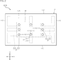
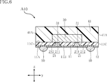
- FIG. 1 It is a top view of the semiconductor device which concerns on 1st Embodiment, and is transmitted through a sealing resin. It is a plan view corresponding to FIG. 1, and is further transmitted through a semiconductor element. It is a bottom view of the semiconductor device shown in FIG. 1. It is a bottom view corresponding to FIG. 3, and is transparent to a protective layer and a plurality of terminals. It is sectional drawing which follows the VV line of FIG. It is sectional drawing which follows the VI-VI line of FIG. It is a partially enlarged view of FIG. It is a partially enlarged view of FIG. FIG. 3 is a partially enlarged cross-sectional view taken along the line IX-IX of FIG. FIG. 7 is a partially enlarged view of FIG. 7.
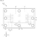
- FIG. 21 is a bottom view of the semiconductor device shown in FIG. It is a bottom view corresponding to FIG. 23, and is transparent to a protective layer and a plurality of terminals.
- 22 is a cross-sectional view taken along the line XXV-XXV of FIG. 22. 22 is a cross-sectional view taken along the line XXVI-XXVI of FIG. 22.
- FIG. 26 is a partially enlarged view. 22 is a partially enlarged cross-sectional view taken along the line XXVIII-XVIII of FIG. 22.
- the semiconductor device A10 includes a first insulating layer 11, a plurality of first wiring layers 21, a semiconductor element 30, a sealing resin 41, a protective layer 42, and a plurality of terminals 50.
- the semiconductor device A10 is surface-mounted on a wiring board.
- the semiconductor device A10 includes a single semiconductor element 30.
- the semiconductor device A10 may include a plurality of semiconductor elements 30.
- the plurality of semiconductor elements 30 include a laser diode and a switching element such as a MOSFET. In this configuration, when the switching element is driven, the laser diode emits light in a pulse shape at intervals of several ns.
- FIG. 1 the sealing resin 41 is transmitted, and in FIG. 2, the semiconductor element 30 is further transmitted with respect to FIG. In FIG. 4, the protective layer 42 and the plurality of terminals 50 are transmitted through.
- FIG. 2 the outer shape of the semiconductor element 30 is shown by an imaginary line (dashed-dotted line).
- the three directions orthogonal to each other are appropriately referred to.
- these are the first direction x, the second direction y, and the thickness direction z, but the present disclosure is not limited thereto.
- the thickness direction z corresponds to, for example, a direction penetrating the thickness of the first insulating layer 11.
- the outer shape of the semiconductor device A10 is rectangular when viewed along the thickness direction z.
- the first direction x is parallel to one side (first side) of the semiconductor device A10
- the second direction y is parallel to another side (second side orthogonal to the first side) of the semiconductor device A10.
- the first side is longer than the second side, but the present disclosure is not limited to this.
- the first insulating layer 11 faces the semiconductor element 30 in the thickness direction z.
- the first insulating layer 11 contains a thermosetting synthetic resin and an additive containing a metal element constituting a part of each of the plurality of first wiring layers 21 (first base layer 21A described later). It consists of materials.
- the synthetic resin is, for example, an epoxy resin or a polyimide.
- the first insulating layer 11 has a first main surface 11A, a first back surface 11B, and a plurality of end surfaces 11C.
- the first main surface 11A and the first back surface 11B face each other in the thickness direction z. Of these, the first main surface 11A faces the semiconductor element 30.
- the plurality of end faces 11C are connected to the first main surface 11A and the first back surface 11B.
- Each of the plurality of end faces 11C faces either the first direction x or the second direction y.
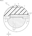
- the first insulating layer 11 has a plurality of first penetration portions 111.
- Each of the plurality of first penetrating portions 111 extends from the side where the first main surface 11A is located to the side where the first back surface 11B is located in the thickness direction z, and penetrates the first insulating layer 11 in the thickness direction z. doing.
- Each of the plurality of first penetration portions 111 is defined by any one of the plurality of first inner peripheral surfaces 111A of the first insulating layer 11.
- Each of the plurality of first inner peripheral surfaces 111A is inclined with respect to the first main surface 11A.
- Each of the plurality of first inner peripheral surfaces 111A has a plurality of first surfaces defined by the first inner peripheral surface 111A from the side where the first back surface 11B is located to the side where the first main surface 11A is located in the thickness direction z. Take a posture of falling toward one of the penetrating portions 111. Therefore, the cross-sectional area of each of the plurality of first penetrating portions 111 with respect to the thickness direction z gradually increases from the side where the first main surface 11A is located to the side where the first back surface 11B is located.
- the first insulating layer 11 has a plurality of first groove portions 112.
- Each of the plurality of first groove portions 112 is recessed from the first back surface 11B in the thickness direction z.
- Each of the plurality of first groove portions 112 is connected to any of the plurality of first penetration portions 111.
- each of the plurality of first groove portions 112 extends along a direction orthogonal to the thickness direction z.
- each pair of side surfaces of the plurality of first groove portions 112 is inclined with respect to the first back surface 11B.
- the width b1 of the first groove portion 112 at the boundary between the pair of side surfaces and the bottom surface of the first groove portion 112 is the boundary between the pair of side surfaces and the first back surface 11B. It is smaller than the width b2 of the first groove portion 112 in the above.
- the plurality of first wiring layers 21 are arranged in the first insulating layer 11 as shown in FIGS. 5 and 6.
- the plurality of first wiring layers 21 form a part of the conductive path between the wiring board on which the semiconductor device A10 is mounted and the semiconductor element 30.
- Each of the plurality of first wiring layers 21 includes a first communication unit 211 and a first main unit 212.
- the first connecting portion 211 is housed in one of a plurality of first penetrating portions 111 of the first insulating layer 11.
- the first connecting portion 211 is in contact with any of a plurality of first inner peripheral surfaces 111A defining the first penetrating portion 111.
- the first communication unit 211 is connected to one of a plurality of electrodes 31 (details will be described later) of the semiconductor element 30.
- the first main portion 212 is connected to the first communication portion 211 of any one of the plurality of first wiring layers 21, and the first back surface 11B is located in the first insulating layer 11. It is placed on the side. More specifically, the first main portion 212 is arranged in any of the plurality of first groove portions 112 of the first insulating layer 11. The first main portion 212 is in contact with the first groove portion 112. As shown in FIGS. 7 to 9, in the semiconductor device A10, a part of the first main portion 212 of each of the plurality of first wiring layers 21 protrudes from any of the plurality of first groove portions 112.
- each of the first connecting portion 211 and the first main portion 212 of the plurality of first wiring layers 21 has a first base layer 21A and a first plating layer 21B.
- the first base layer 21A is composed of a metal element contained in the additive contained in the first insulating layer 11.
- the first base layer 21A is in contact with the first insulating layer 11.
- Each of the plurality of first inner peripheral surfaces 111A of the first insulating layer 11 is covered with a first base layer 21A forming the first connecting portion 211 of any one of the plurality of first wiring layers 21.
- the first plating layer 21B covers the first base layer 21A of any one of the plurality of first wiring layers 21.
- the first plating layer 21B is made of a material containing, for example, copper (Cu). As shown in FIG. 9, the first plating layer 21B of each of the first main portions 212 of the plurality of first wiring layers 21 has a recess 212A recessed in the thickness direction z. The recess 212A extends along the direction in which any of the plurality of first groove portions 112 of the first insulating layer 11 extends.
- the semiconductor element 30 is arranged in contact with the first main surface 11A of the first insulating layer 11.
- the semiconductor element 30 is a flip chip mounting type.
- the semiconductor device 30 has a plurality of electrodes 31.
- the plurality of electrodes 31 are provided on either side of the thickness direction z in the semiconductor element 30.
- the plurality of electrodes 31 are provided on the side closer to the first main surface 11A in the thickness direction z.
- Each of the plurality of electrodes 31 is conducting to the circuit configured in the semiconductor element 30.
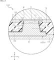
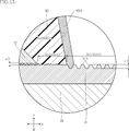
- Each of the plurality of electrodes 31 is composed of a single metal layer or a plurality of metal layers laminated in the thickness direction z. As shown in FIG.
- each of the plurality of electrodes 31 has a connecting surface 311.
- the connection surface 311 faces the same side as the first back surface 11B of the first insulating layer 11 in the thickness direction z.
- Each of the first communication portions 211 of the plurality of first wiring layers 21 is connected to the connection surface 311 of any one of the plurality of electrodes 31.
- the semiconductor element 30 is conductive to the plurality of first wiring layers 21.
- the semiconductor element 30 has a passivation film 32.
- the passivation film 32 is in contact with the first main surface 11A in the semiconductor element 30.
- the passivation film 32 is in contact with each of the plurality of electrodes 31.
- the passivation film 32 is made of a material containing, for example, polyimide.
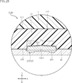
- each connection surface 311 of the plurality of electrodes 31 has a first region 311A and a second region 311B.
- the first region 311A is exposed from the first insulating layer 11 by any of the plurality of first penetrating portions 111 of the first insulating layer 11.
- the first plating layer 21B of the first connecting portion 211 is in contact with the first region 311A of any of the plurality of electrodes 31.
- the second region 311B is covered with the first insulating layer 11. As shown in FIG.
- the surface roughness sr1 of the first region 311A is larger than the surface roughness sr2 of the second region 311B.
- the surface roughness sr1 and sr2 are the bottommost portion of each connection surface 311 of the plurality of electrodes 31 located inward of the electrode 31 in the thickness direction z, and the thickness direction from the bottommost portion. It is the distance in the thickness direction z from the highest portion located farthest in z.
- the sealing resin 41 is arranged in contact with the first main surface 11A of the first insulating layer 11 and covers a part of the semiconductor element 30.
- the sealing resin 41 is made of a material containing, for example, a black epoxy resin.
- the sealing resin 41 has a plurality of side surfaces 41A. Each of the plurality of side surfaces 41A faces either the first direction x or the second direction y. Each of the plurality of side surfaces 41A is flush with any of the plurality of end faces 11C of the first insulating layer 11.
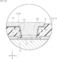
- the protective layer 42 covers the first back surface 11B of the first insulating layer 11 and the first main portion 212 of the plurality of first wiring layers 21.
- the protective layer 42 faces the wiring board.
- the protective layer 42 has electrical insulation.
- the protective layer 42 is made of, for example, a material containing polyimide.
- the protective layer 42 has a plurality of openings 421. The plurality of openings 421 penetrate the protective layer 42 in the thickness direction z. A part of the first main portion 212 of each of the plurality of first wiring layers 21 is exposed from the protective layer 42 by any of the plurality of openings 421.
- the plurality of terminals 50 are individually bonded to a part of the first main portion 212 of the plurality of first wiring layers 21 exposed from the plurality of openings 421 of the protective layer 42. ing.
- the plurality of terminals 50 are used for mounting the semiconductor device A10 on the wiring board.
- the plurality of terminals 50 project from the protective layer 42 in the thickness direction z.
- each of the plurality of terminals 50 has a base portion 51 and a bump portion 52.
- the base 51 is in contact with any part of the first main portion 212 of the plurality of first wiring layers 21.
- the base 51 is a plurality of metal layers in which a nickel (Ni) layer, a palladium layer (Pd), and a gold (Au) layer are laminated in this order in a direction away from the first back surface 11B of the first insulating layer 11 in the thickness direction z. Consists of. Here, among these metal layers, the palladium layer may not be provided.
- the bump portion 52 is in contact with both the base portion 51 and the protective layer 42.
- the bump portion 52 includes a portion protruding from the protective layer 42 in the thickness direction z.
- the bump portion 52 is made of a material containing tin (Sn).
- the bump portion 52 is made of, for example, lead-free solder.
- FIGS. 11 to 20 An example of a method for manufacturing the semiconductor device A10 will be described with reference to FIGS. 11 to 20.
- the cross-sectional positions of FIGS. 11 to 20 (excluding FIGS. 14, 15 and 17) are the same as the cross-sectional positions of FIG.
- the semiconductor element 30 is embedded in the sealing resin 81.
- the sealing resin 81 is made of a material containing a black epoxy resin.
- compression molding is performed.
- the semiconductor element 30 is embedded in the sealing resin 81.
- the plurality of electrodes 31 are exposed from the sealing resin 81.
- an insulating layer 82 is formed, which is laminated on the sealing resin 81 and covers a plurality of electrodes 31 of the semiconductor element 30.
- the insulating layer 82 is made of a material containing a thermosetting synthetic resin and an additive containing a metal element constituting a part of a plurality of wiring layers 83 (details will be described later).
- the synthetic resin is an epoxy resin or a polyimide.
- the insulating layer 82 is formed by compression molding.
- each of the plurality of wiring layers 83 includes a first communication unit 211 and a first main unit 212.
- the step of forming the plurality of wiring layers 83 includes a step of precipitating the base layer 83A on the insulating layer 82 and a step of forming a plating layer 83B covering the base layer 83A.
- the base layer 83A is deposited on the insulating layer 82.
- the base layer 83A is composed of the metal element contained in the additive contained in the insulating layer 82.
- a plurality of through portions 821 and a plurality of groove portions 822 are formed in the insulating layer 82.
- the plurality of penetrating portions 821 penetrate the insulating layer 82 in the thickness direction z. Each of the plurality of penetration portions 821 exposes a part of the surface (connection surface 311) of any of the plurality of electrodes 31 of the semiconductor element 30 from the insulating layer 82.
- Each of the plurality of groove portions 822 is recessed from the surface 82A of the insulating layer 82 and is connected to any of the plurality of through portions 821.
- the front surface 82A corresponds to the first back surface 11B of the first insulating layer 11.
- the plurality of penetration portions 821 and the plurality of groove portions 822 are formed by irradiating the insulating layer 82 with a laser while recognizing the positions of the plurality of electrodes 31 with an infrared camera.
- the laser irradiation position on the insulating layer 82 is corrected one by one based on the position information of the plurality of electrodes 31 obtained by image recognition.
- the laser is an ultraviolet laser having a wavelength of 355 nm and a beam diameter of 17 ⁇ m.
- Concavo-convex 31A is formed in one region 311A) by laser irradiation.
- the metal element contained in the additive contained in the insulating layer 82 is excited.
- a base layer 83A that covers the inner peripheral surface 821A of the insulating layer 82 that individually defines the plurality of penetrating portions 821 and the plurality of groove portions 822 is formed.
- a plating layer 83B covering the base layer 83A is formed.
- the plating layer 83B is made of a material containing copper.
- the plating layer 83B is formed by electroless plating, electrolytic plating, or a combination thereof.
- each of the plurality of penetration portions 821 is formed with the first communication portion 211 of any of the plurality of wiring layers 83.
- each of the plurality of groove portions 822 is formed with the first main portion 212 of any one of the plurality of wiring layers 83.
- the plurality of wiring layers 83 are formed.
- a protective layer 84 is formed which is laminated on the insulating layer 82 and covers the first main portion 212 of the plurality of wiring layers 83.
- the protective layer 84 has a plurality of openings 841 penetrating in the thickness direction z.
- the photosensitive polyimide is applied to the surface of the insulating layer 82 and the surfaces of the plurality of wiring layers 83 using a spin coater.
- a plurality of openings 841 are formed in the photosensitive polyimide by photolithography patterning. As a result, a part of the first main portion 212 of each of the plurality of wiring layers 83 is exposed from the protective layer 84 by any of the plurality of openings 841.
- a plurality of terminals 50 individually bonded to a part of the first main portion 212 of the plurality of wiring layers 83 exposed by the plurality of openings 841 of the protective layer 84 are formed.
- the base 51 of the plurality of terminals 50 shown in FIG. 8 is formed.
- the base 51 is formed by electroless plating.
- the bump portions 52 of the plurality of terminals 50 shown in FIG. 8 are formed.
- the bump portion 52 is formed by melting a conductive material containing tin such as lead-free solder by reflow and then solidifying it by cooling. As a result, a plurality of terminals 50 are formed.
- the sealing resin 81, the insulating layer 82, and the protective layer 84 are cut into a plurality of pieces by cutting along the cutting line CL with a dicing blade or the like.
- the individual piece includes one semiconductor element 30 and a plurality of wiring layers 83 connected to the semiconductor element 30.
- the sealing resin 81, the insulating layer 82, and the protective layer 84, which are individually formed by this step, correspond to the sealing resin 41, the first insulating layer 11, and the protective layer 42 of the semiconductor device A10. Through the above steps, the semiconductor device A10 is manufactured.
- the first connecting portion 211 of the first wiring layer 21 of the semiconductor device A10 is housed in the first penetrating portion 111 of the first insulating layer 11 and is connected to the electrode 31 of the semiconductor element 30.
- the electrode 31 has a connecting surface 311 including a first region 311A and a second region 311B.
- the first region 311A is exposed from the first insulating layer 11 at the first penetrating portion 111.
- the second region 311B is covered with the first insulating layer 11.
- the first communication unit 211 is in contact with the first region 311A. As shown in FIG. 10, the surface roughness sr1 of the first region 311A is larger than the surface roughness sr2 of the second region 311B.
- the surface area per unit area of the first region 311A becomes larger than the surface area per unit area of the second region 311B. Therefore, the contact area of the first contact portion 211 with respect to the first region 311A increases. Further, the anchoring effect (anchor effect) of the first communication unit 211 with respect to the first region 311A is exhibited. Therefore, according to the semiconductor device A10, it is possible to further improve the adhesion of the wiring layer (first wiring layer 21) to the electrode 31 of the semiconductor element 30.
- the step of forming the wiring layer 83 according to the manufacturing method of the semiconductor device A10 includes a step of precipitating the base layer 83A on the insulating layer 82.
- the through portion 821 that exposes a part of the surface (connection surface 311) of the electrode 31 of the semiconductor element 30 from the insulating layer 82 is formed by laser irradiation, so that the inside of the insulating layer 82 that defines the through portion 821 is formed.
- the base layer 83A covering the peripheral surface 821A is deposited.
- the laser forms unevenness 31A on a part of the surface of the electrode 31 exposed from the insulating layer 82 at the penetrating portion 821.
- the surface of the electrode 31, that is, the connection surface 311 of the electrode 31 can be configured to include the first region 311A and the second region 311B.
- the penetrating portion 821 is formed on the insulating layer 82, the insulating layer 82 is irradiated with the laser while recognizing the position of the electrode 31 as an image.
- the first region 311A and the second region 311B are configured to be accurately separated on the surface of the electrode 31 (connection surface 311).
- the first inner peripheral surface 111A defining the first penetrating portion 111 of the first insulating layer 11 is the first lower surface by including the step of precipitating the base layer 83A on the insulating layer 82. It will be covered with the stratum 21A.
- the first inner peripheral surface 111A is inclined with respect to the first main surface 11A of the first insulating layer 11. Further, the cross-sectional area of the first penetrating portion 111 with respect to the thickness direction z gradually increases from the side where the first main surface 11A is located to the side where the first back surface 11B is located. This is a configuration obtained by irradiating a laser from the surface 82A of the insulating layer 82 toward the surface (connecting surface 311) of the electrode 31 when the penetrating portion 821 is formed in the insulating layer 82.
- a groove portion 822 that is recessed from the surface 82A of the insulating layer 82 and is connected to the penetrating portion 821 is formed in the insulating layer 82 by laser irradiation.
- the base layer 83A covering the groove portion 822 is deposited. Therefore, the patterning of the wiring layer 83 can be freely performed by laser irradiation.
- the step of forming the wiring layer 83 according to the manufacturing method of the semiconductor device A10 includes a step of forming a plating layer 83B covering the base layer 83A.
- the plating layer 83B is formed by electroless plating, electrolytic plating, or a combination thereof.
- the forming method by electroless plating provides a conductive path necessary for performing the electrolytic plating on the surface 82A of the insulating layer 82 as compared with the forming method by electroplating. Is unnecessary. Therefore, the wiring layer 83 can be formed more efficiently.
- the semiconductor device A10 includes a protective layer 42 and terminals 50.
- the protective layer 42 covers the first back surface 11B of the first insulating layer 11 and the first main portion 212 of the first wiring layer 21.
- the protective layer 42 has an opening 421 in which a part of the first main portion 212 is exposed from the protective layer 42.
- the terminal 50 is joined to a part of the first main portion 212 exposed from the protective layer 42 at the opening 421, and protrudes from the protective layer 42 in the thickness direction.
- the terminal 50 made of a material containing tin, when the semiconductor device A10 is mounted on the wiring board, at least a part of the terminal 50 is melted by the reflow. As a result, the effect of self-repairing the positional deviation of the semiconductor device A10 with respect to the wiring board (self-alignment effect) can be obtained.
- the semiconductor device A20 according to the second embodiment will be described with reference to FIGS. 21 to 28.
- the same or similar elements as the above-mentioned semiconductor device A10 are designated by the same reference numerals, and duplicate description will be omitted.
- the semiconductor device A20 further includes the second insulating layer 12 and the plurality of second wiring layers 22, and the configuration of the protective layer 42 and the plurality of terminals 50 is different from that of the semiconductor device A10.
- the sealing resin 41 is transmitted, and in FIG. 22, the first insulating layer 11 and the semiconductor element 30 are further transmitted with respect to FIG. 21.
- the protective layer 42 and the plurality of terminals 50 are transmitted through.
- the outer shape of the transmitted semiconductor element 30 is shown by an imaginary line.
- the second insulating layer 12 is arranged in contact with the first back surface 11B of the first insulating layer 11.
- the first insulating layer 11 has a structure sandwiched between the second insulating layer 12 and the sealing resin 41 in the thickness direction z.
- the second insulating layer 12 contains a thermosetting synthetic resin and an additive containing a metal element constituting a part of each of the plurality of second wiring layers 22 (second base layer 22A described later). It consists of materials.
- the synthetic resin is, for example, an epoxy resin or a polyimide.
- the second insulating layer 12 has a second main surface 12A, a second back surface 12B, and a plurality of end surfaces 12C.
- the second main surface 12A and the second back surface 12B face opposite to each other in the thickness direction z. Of these, the second main surface 12A is in contact with the first back surface 11B.
- the plurality of end faces 12C are connected to the second main surface 12A and the second back surface 12B. Each of the plurality of end faces 12C faces either the first direction x or the second direction y. Each of the plurality of end faces 12C is flush with both of the plurality of end faces 11C of the first insulating layer 11 and any of the plurality of side surfaces 41A of the sealing resin 41.
- the second insulating layer 12 has a plurality of second penetration portions 121.
- Each of the plurality of second penetrating portions 121 extends from the side where the second main surface 12A is located to the side where the second back surface 12B is located in the thickness direction z, and penetrates the second insulating layer 12 in the thickness direction z. doing.
- Each of the plurality of second penetration portions 121 is defined by any one of the plurality of second inner peripheral surfaces 121A of the second insulating layer 12.
- Each of the plurality of second inner peripheral surfaces 121A is inclined with respect to the second main surface 12A.
- Each of the plurality of second inner peripheral surfaces 121A has a plurality of second surfaces defined by the second inner peripheral surface 121A from the side where the second back surface 12B is located to the side where the second main surface 12A is located in the thickness direction z. Take a posture of falling toward any of the penetrating portions 121. Therefore, the cross-sectional area of each of the plurality of second penetrating portions 121 with respect to the thickness direction z gradually increases from the side where the second main surface 12A is located to the side where the second back surface 12B is located.
- the second insulating layer 12 has a plurality of second groove portions 122.
- Each of the plurality of second groove portions 122 is recessed from the second back surface 12B in the thickness direction z.
- Each of the plurality of second groove portions 122 is connected to any of the plurality of second through portions 121.
- each of the plurality of second groove portions 122 extends along a direction orthogonal to the thickness direction z.
- each pair of side surfaces of the plurality of second groove portions 122 is inclined with respect to the second back surface 12B.
- the width b3 of the second groove portion 122 at the boundary between the pair of side surfaces and the bottom surface of the second groove portion 122 is the boundary between the pair of side surfaces and the second back surface 12B. It is smaller than the width b4 of the second groove portion 122 in the above.
- the plurality of second wiring layers 22 are arranged in the second insulating layer 12.
- the plurality of second wiring layers 22 together with the plurality of first wiring layers 21 form a part of the conductive path between the wiring board on which the semiconductor device A10 is mounted and the semiconductor element 30.
- Each of the plurality of second wiring layers 22 includes a second communication unit 221 and a second main unit 222.
- the second connecting portion 221 is housed in one of a plurality of second penetrating portions 121 of the second insulating layer 12.
- the second communication unit 221 is in contact with any of the plurality of second inner peripheral surfaces 121A defining the second penetration portion 121.
- the second communication unit 221 is connected to the first main unit 212 of any one of the plurality of first wiring layers 21.
- the second main portion 222 is connected to the second connecting portion 221 of any one of the plurality of second wiring layers 22, and the second back surface 12B is located in the second insulating layer 12. It is placed on the side. More specifically, the second main portion 222 is arranged in any of the plurality of second groove portions 122 of the second insulating layer 12. The second main portion 222 is in contact with the second groove portion 122.
- FIGS. 27 and 28 in the semiconductor device A20, a part of the second main portion 222 of each of the plurality of second wiring layers 22 protrudes from any of the plurality of second groove portions 122.
- each of the plurality of second penetration portions 121 of the second insulating layer 12 is any of the plurality of first wiring layers 21. It overlaps with the first main part 212.
- the second main portion 222 of each of the plurality of second wiring layers 22 is the first main portion 212 of any one of the plurality of first wiring layers 21.
- the first main portion 212 extends in a direction different from the extending direction.
- each of the second connecting portion 221 and the second main portion 222 of the plurality of second wiring layers 22 has a second base layer 22A and a second plating layer 22B.
- the second base layer 22A is composed of the metal element contained in the additive contained in the second insulating layer 12.
- the second base layer 22A is in contact with the second insulating layer 12.
- Each of the plurality of second inner peripheral surfaces 121A of the second insulating layer 12 is covered with a second base layer 22A forming the second connecting portion 221 of any of the plurality of second wiring layers 22.
- the second plating layer 22B covers the second base layer 22A of any one of the plurality of second wiring layers 22.
- the second plating layer 22B is made of, for example, a material containing copper.
- the second plating layer 22B is in contact with the first main portion 212 of any one of the plurality of first wiring layers 21.
- the second plating layer 22B of each of the second main portions 222 of the plurality of second wiring layers 22 has a recess 222A recessed in the thickness direction z.
- the recess 222A extends along a direction in which any of the plurality of second groove portions 122 of the second insulating layer 12 extends.
- the protective layer 42 covers the second back surface 12B of the second insulating layer 12 and the second main portion 222 of the plurality of second wiring layers 22.
- the protective layer 42 faces the wiring board.
- a part of the second main portion 222 of each of the plurality of second wiring layers 22 is exposed from the protective layer 42 by any of the plurality of openings 421.
- the plurality of terminals 50 are individually joined to a part of the second main portion 222 of the plurality of second wiring layers 22 exposed from the plurality of openings 421.
- the first connecting portion 211 of the first wiring layer 21 of the semiconductor device A20 is housed in the first penetrating portion 111 of the first insulating layer 11 and is connected to the electrode 31 of the semiconductor element 30.
- the electrode 31 has a connecting surface 311 including a first region 311A and a second region 311B.
- the first region 311A is exposed from the first insulating layer 11 at the first penetrating portion 111.
- the second region 311B is covered with the first insulating layer 11.
- the first communication unit 211 is in contact with the first region 311A.
- the surface roughness sr1 of the first region 311A is larger than the surface roughness sr2 of the second region 311B. Therefore, the semiconductor device A20 can also further improve the adhesion of the wiring layer (first wiring layer 21) to the electrode 31 of the semiconductor element 30.
- the semiconductor device A20 has a second insulating layer 12 having a second main surface 12A, a second back surface 12B, and a second penetrating portion 121, and a second wiring layer 22 having a second connecting portion 221 and a second main portion 222. Further prepare.
- the second main surface 12A is in contact with the first back surface 11B of the first insulating layer 11.
- the second connecting portion 221 is housed in the second penetrating portion 121 and is connected to the first main portion 212 of the first wiring layer 21.
- the second main portion 222 is connected to the second connecting portion 221 and is arranged on the side of the second insulating layer 12 where the second back surface 12B is located.
- the first main portion 212 is covered with the second insulating layer 12.
- the semiconductor device A20 When viewed along the thickness direction z, at least a part of the second penetrating portion 121 overlaps with the first main portion 212. As a result, in the semiconductor device A20, the second main portion 222 becomes the first main portion 222 when viewed along the thickness direction z without causing a short circuit in the conduction path between the first wiring layer 21 and the second wiring layer 22. It is possible to take an arrangement form that overlaps with the portion 212. Therefore, according to the semiconductor device A20, a conduction path more complicated than that of the semiconductor device A10 can be configured.
- the present disclosure is not limited to the above-described embodiment, and the specific configuration of each part of the semiconductor device can be freely redesigned. ..
- the configuration may include a plurality of semiconductor elements 30.
- the type of each semiconductor element 30 can be selected according to the required application and function.
- various components having a rectangular outer shape as viewed along the thickness direction z are used, but the present disclosure is not limited to this, and the outer shape is, for example, a circular shape or a hexagonal shape. And so on.
Landscapes
- Engineering & Computer Science (AREA)
- Computer Hardware Design (AREA)
- Microelectronics & Electronic Packaging (AREA)
- Power Engineering (AREA)
- Physics & Mathematics (AREA)
- Condensed Matter Physics & Semiconductors (AREA)
- General Physics & Mathematics (AREA)
- Internal Circuitry In Semiconductor Integrated Circuit Devices (AREA)
- Structures Or Materials For Encapsulating Or Coating Semiconductor Devices Or Solid State Devices (AREA)
Abstract
Dispositif à semi-conducteur pourvu d'une couche d'isolation, d'un élément semi-conducteur, d'une couche de câblage et d'une résine d'étanchéité. La couche d'isolation possède une surface principale et une surface inverse espacée l'une de l'autre dans la direction d'épaisseur, et possède, formée dans celle-ci, une partie de pénétration s'étendant dans la direction d'épaisseur. L'élément semi-conducteur comporte une électrode correspondant à la partie de pénétration et est en contact avec la surface principale. La partie de câblage comprend une partie de liaison qui est logée dans la partie de pénétration et est en contact avec l'électrode, et une partie principale qui est continue à partir de la partie de liaison et qui est positionnée sur la surface arrière. La résine d'étanchéité est en contact avec la surface principale et recouvre l'élément semi-conducteur. L'électrode présente une surface de connexion faisant face à la partie de liaison La surface de connexion comprend une première région qui est exposée à partir de la couche d'isolation par la partie de pénétration, et une seconde région en contact avec la couche d'isolation. La rugosité de surface de la première région est plus élevée que la rugosité de surface de la seconde région.
Priority Applications (4)
| Application Number | Priority Date | Filing Date | Title |
|---|---|---|---|
| DE112021002956.8T DE112021002956T5 (de) | 2020-05-26 | 2021-05-21 | Halbleiterbauteil und verfahren zum herstellen eines halbleiterbauteils |
| JP2022526992A JPWO2021241447A1 (fr) | 2020-05-26 | 2021-05-21 | |
| US17/925,719 US20230197544A1 (en) | 2020-05-26 | 2021-05-21 | Semiconductor device and method for manufacturing semiconductor device |
| CN202180037156.5A CN115699295A (zh) | 2020-05-26 | 2021-05-21 | 半导体装置以及半导体装置的制造方法 |
Applications Claiming Priority (2)
| Application Number | Priority Date | Filing Date | Title |
|---|---|---|---|
| JP2020091169 | 2020-05-26 | ||
| JP2020-091169 | 2020-05-26 |
Publications (1)
| Publication Number | Publication Date |
|---|---|
| WO2021241447A1 true WO2021241447A1 (fr) | 2021-12-02 |
Family
ID=78744674
Family Applications (1)
| Application Number | Title | Priority Date | Filing Date |
|---|---|---|---|
| PCT/JP2021/019392 WO2021241447A1 (fr) | 2020-05-26 | 2021-05-21 | Dispositif à semi-conducteur et procédé de fabrication de dispositif à semi-conducteur |
Country Status (5)
| Country | Link |
|---|---|
| US (1) | US20230197544A1 (fr) |
| JP (1) | JPWO2021241447A1 (fr) |
| CN (1) | CN115699295A (fr) |
| DE (1) | DE112021002956T5 (fr) |
| WO (1) | WO2021241447A1 (fr) |
Citations (5)
| Publication number | Priority date | Publication date | Assignee | Title |
|---|---|---|---|---|
| JP2008294415A (ja) * | 2007-04-27 | 2008-12-04 | Sanyo Electric Co Ltd | 素子搭載用基板およびその製造方法、半導体モジュールおよびその製造方法、ならびに携帯機器 |
| JP2009177072A (ja) * | 2008-01-28 | 2009-08-06 | Fujikura Ltd | 半導体装置及びその製造方法 |
| JP2017069257A (ja) * | 2015-09-28 | 2017-04-06 | 日立化成株式会社 | 半導体装置の製造方法 |
| JP2018019071A (ja) * | 2016-07-14 | 2018-02-01 | 住友ベークライト株式会社 | 半導体装置の製造方法 |
| WO2018047770A1 (fr) * | 2016-09-08 | 2018-03-15 | 住友ベークライト株式会社 | Procédé de fabrication de dispositif à semi-conducteur |
Family Cites Families (1)
| Publication number | Priority date | Publication date | Assignee | Title |
|---|---|---|---|---|
| JP5976073B2 (ja) | 2014-11-07 | 2016-08-23 | 日東電工株式会社 | 半導体装置の製造方法 |
-
2021
- 2021-05-21 CN CN202180037156.5A patent/CN115699295A/zh active Pending
- 2021-05-21 JP JP2022526992A patent/JPWO2021241447A1/ja active Pending
- 2021-05-21 WO PCT/JP2021/019392 patent/WO2021241447A1/fr active Application Filing
- 2021-05-21 US US17/925,719 patent/US20230197544A1/en active Pending
- 2021-05-21 DE DE112021002956.8T patent/DE112021002956T5/de active Pending
Patent Citations (5)
| Publication number | Priority date | Publication date | Assignee | Title |
|---|---|---|---|---|
| JP2008294415A (ja) * | 2007-04-27 | 2008-12-04 | Sanyo Electric Co Ltd | 素子搭載用基板およびその製造方法、半導体モジュールおよびその製造方法、ならびに携帯機器 |
| JP2009177072A (ja) * | 2008-01-28 | 2009-08-06 | Fujikura Ltd | 半導体装置及びその製造方法 |
| JP2017069257A (ja) * | 2015-09-28 | 2017-04-06 | 日立化成株式会社 | 半導体装置の製造方法 |
| JP2018019071A (ja) * | 2016-07-14 | 2018-02-01 | 住友ベークライト株式会社 | 半導体装置の製造方法 |
| WO2018047770A1 (fr) * | 2016-09-08 | 2018-03-15 | 住友ベークライト株式会社 | Procédé de fabrication de dispositif à semi-conducteur |
Also Published As
| Publication number | Publication date |
|---|---|
| US20230197544A1 (en) | 2023-06-22 |
| CN115699295A (zh) | 2023-02-03 |
| JPWO2021241447A1 (fr) | 2021-12-02 |
| DE112021002956T5 (de) | 2023-03-09 |
Similar Documents
| Publication | Publication Date | Title |
|---|---|---|
| JP5123664B2 (ja) | 半導体装置およびその製造方法 | |
| US7968446B2 (en) | Metallic bump structure without under bump metallurgy and manufacturing method thereof | |
| TWI675497B (zh) | 發光裝置封裝及搭載發光裝置之封裝 | |
| US8035033B2 (en) | Wiring substrate with plurality of wiring and insulating layers with a solder resist layer covering a wiring layer on the outside of outer insulating layer but exposing the holes in the outer insulating layer | |
| JPH10135270A (ja) | 半導体装置及びその製造方法 | |
| JP2000138313A (ja) | 半導体装置及びその製造方法 | |
| JP4489821B2 (ja) | 半導体装置及びその製造方法 | |
| JP2006128455A (ja) | 半導体装置およびその製造方法 | |
| US10121695B2 (en) | Semiconductor device | |
| JP5406572B2 (ja) | 電子部品内蔵配線基板及びその製造方法 | |
| JP2012015438A (ja) | 半導体発光装置 | |
| JP2016021534A (ja) | プリント配線板およびその製造方法 | |
| JP6392163B2 (ja) | 配線基板及びその製造方法、半導体装置 | |
| WO2021241447A1 (fr) | Dispositif à semi-conducteur et procédé de fabrication de dispositif à semi-conducteur | |
| JP2023099739A (ja) | 半導体装置 | |
| JP6752639B2 (ja) | 半導体装置の製造方法 | |
| JP4877779B2 (ja) | 発光ダイオード装置及びその製造方法 | |
| JP2009152408A (ja) | 半導体装置およびその製造方法 | |
| JP2007012716A (ja) | 半導体装置 | |
| JP2006156574A (ja) | 回路装置およびその製造方法 | |
| JP2021190454A (ja) | 半導体装置、および半導体装置の製造方法 | |
| KR20100048622A (ko) | 범핑 하지 금속이 없는 금속 범프 구조 및 그 제조방법 | |
| JP2021125624A (ja) | 半導体装置 | |
| JP2021027122A (ja) | 半導体装置 | |
| JP2013254984A (ja) | 半導体装置 |
Legal Events
| Date | Code | Title | Description |
|---|---|---|---|
| 121 | Ep: the epo has been informed by wipo that ep was designated in this application |
Ref document number: 21814631 Country of ref document: EP Kind code of ref document: A1 |
|
| ENP | Entry into the national phase |
Ref document number: 2022526992 Country of ref document: JP Kind code of ref document: A |
|
| 122 | Ep: pct application non-entry in european phase |
Ref document number: 21814631 Country of ref document: EP Kind code of ref document: A1 |