WO2021241447A1 - Semiconductor device and method for manufacturing semiconductor device - Google Patents
Semiconductor device and method for manufacturing semiconductor device Download PDFInfo
- Publication number
- WO2021241447A1 WO2021241447A1 PCT/JP2021/019392 JP2021019392W WO2021241447A1 WO 2021241447 A1 WO2021241447 A1 WO 2021241447A1 JP 2021019392 W JP2021019392 W JP 2021019392W WO 2021241447 A1 WO2021241447 A1 WO 2021241447A1
- Authority
- WO
- WIPO (PCT)
- Prior art keywords
- insulating layer
- layer
- semiconductor device
- main
- thickness direction
- Prior art date
Links
Images


Classifications
-
- H—ELECTRICITY
- H01—ELECTRIC ELEMENTS
- H01L—SEMICONDUCTOR DEVICES NOT COVERED BY CLASS H10
- H01L23/00—Details of semiconductor or other solid state devices
- H01L23/48—Arrangements for conducting electric current to or from the solid state body in operation, e.g. leads, terminal arrangements ; Selection of materials therefor
- H01L23/488—Arrangements for conducting electric current to or from the solid state body in operation, e.g. leads, terminal arrangements ; Selection of materials therefor consisting of soldered or bonded constructions
- H01L23/498—Leads, i.e. metallisations or lead-frames on insulating substrates, e.g. chip carriers
- H01L23/49811—Additional leads joined to the metallisation on the insulating substrate, e.g. pins, bumps, wires, flat leads
- H01L23/49816—Spherical bumps on the substrate for external connection, e.g. ball grid arrays [BGA]
-
- H—ELECTRICITY
- H01—ELECTRIC ELEMENTS
- H01L—SEMICONDUCTOR DEVICES NOT COVERED BY CLASS H10
- H01L23/00—Details of semiconductor or other solid state devices
- H01L23/28—Encapsulations, e.g. encapsulating layers, coatings, e.g. for protection
- H01L23/29—Encapsulations, e.g. encapsulating layers, coatings, e.g. for protection characterised by the material, e.g. carbon
- H01L23/293—Organic, e.g. plastic
-
- H—ELECTRICITY
- H01—ELECTRIC ELEMENTS
- H01L—SEMICONDUCTOR DEVICES NOT COVERED BY CLASS H10
- H01L24/00—Arrangements for connecting or disconnecting semiconductor or solid-state bodies; Methods or apparatus related thereto
- H01L24/01—Means for bonding being attached to, or being formed on, the surface to be connected, e.g. chip-to-package, die-attach, "first-level" interconnects; Manufacturing methods related thereto
- H01L24/02—Bonding areas ; Manufacturing methods related thereto
- H01L24/04—Structure, shape, material or disposition of the bonding areas prior to the connecting process
- H01L24/05—Structure, shape, material or disposition of the bonding areas prior to the connecting process of an individual bonding area
-
- H—ELECTRICITY
- H01—ELECTRIC ELEMENTS
- H01L—SEMICONDUCTOR DEVICES NOT COVERED BY CLASS H10
- H01L24/00—Arrangements for connecting or disconnecting semiconductor or solid-state bodies; Methods or apparatus related thereto
- H01L24/01—Means for bonding being attached to, or being formed on, the surface to be connected, e.g. chip-to-package, die-attach, "first-level" interconnects; Manufacturing methods related thereto
- H01L24/10—Bump connectors ; Manufacturing methods related thereto
- H01L24/15—Structure, shape, material or disposition of the bump connectors after the connecting process
- H01L24/16—Structure, shape, material or disposition of the bump connectors after the connecting process of an individual bump connector
-
- H—ELECTRICITY
- H01—ELECTRIC ELEMENTS
- H01L—SEMICONDUCTOR DEVICES NOT COVERED BY CLASS H10
- H01L24/00—Arrangements for connecting or disconnecting semiconductor or solid-state bodies; Methods or apparatus related thereto
- H01L24/01—Means for bonding being attached to, or being formed on, the surface to be connected, e.g. chip-to-package, die-attach, "first-level" interconnects; Manufacturing methods related thereto
- H01L24/42—Wire connectors; Manufacturing methods related thereto
- H01L24/47—Structure, shape, material or disposition of the wire connectors after the connecting process
- H01L24/48—Structure, shape, material or disposition of the wire connectors after the connecting process of an individual wire connector
-
- H—ELECTRICITY
- H01—ELECTRIC ELEMENTS
- H01L—SEMICONDUCTOR DEVICES NOT COVERED BY CLASS H10
- H01L24/00—Arrangements for connecting or disconnecting semiconductor or solid-state bodies; Methods or apparatus related thereto
- H01L24/73—Means for bonding being of different types provided for in two or more of groups H01L24/10, H01L24/18, H01L24/26, H01L24/34, H01L24/42, H01L24/50, H01L24/63, H01L24/71
-
- H—ELECTRICITY
- H01—ELECTRIC ELEMENTS
- H01L—SEMICONDUCTOR DEVICES NOT COVERED BY CLASS H10
- H01L2224/00—Indexing scheme for arrangements for connecting or disconnecting semiconductor or solid-state bodies and methods related thereto as covered by H01L24/00
- H01L2224/01—Means for bonding being attached to, or being formed on, the surface to be connected, e.g. chip-to-package, die-attach, "first-level" interconnects; Manufacturing methods related thereto
- H01L2224/02—Bonding areas; Manufacturing methods related thereto
- H01L2224/04—Structure, shape, material or disposition of the bonding areas prior to the connecting process
- H01L2224/04042—Bonding areas specifically adapted for wire connectors, e.g. wirebond pads
-
- H—ELECTRICITY
- H01—ELECTRIC ELEMENTS
- H01L—SEMICONDUCTOR DEVICES NOT COVERED BY CLASS H10
- H01L2224/00—Indexing scheme for arrangements for connecting or disconnecting semiconductor or solid-state bodies and methods related thereto as covered by H01L24/00
- H01L2224/01—Means for bonding being attached to, or being formed on, the surface to be connected, e.g. chip-to-package, die-attach, "first-level" interconnects; Manufacturing methods related thereto
- H01L2224/10—Bump connectors; Manufacturing methods related thereto
- H01L2224/15—Structure, shape, material or disposition of the bump connectors after the connecting process
- H01L2224/16—Structure, shape, material or disposition of the bump connectors after the connecting process of an individual bump connector
- H01L2224/161—Disposition
- H01L2224/16151—Disposition the bump connector connecting between a semiconductor or solid-state body and an item not being a semiconductor or solid-state body, e.g. chip-to-substrate, chip-to-passive
- H01L2224/16221—Disposition the bump connector connecting between a semiconductor or solid-state body and an item not being a semiconductor or solid-state body, e.g. chip-to-substrate, chip-to-passive the body and the item being stacked
- H01L2224/16225—Disposition the bump connector connecting between a semiconductor or solid-state body and an item not being a semiconductor or solid-state body, e.g. chip-to-substrate, chip-to-passive the body and the item being stacked the item being non-metallic, e.g. insulating substrate with or without metallisation
-
- H—ELECTRICITY
- H01—ELECTRIC ELEMENTS
- H01L—SEMICONDUCTOR DEVICES NOT COVERED BY CLASS H10
- H01L2224/00—Indexing scheme for arrangements for connecting or disconnecting semiconductor or solid-state bodies and methods related thereto as covered by H01L24/00
- H01L2224/01—Means for bonding being attached to, or being formed on, the surface to be connected, e.g. chip-to-package, die-attach, "first-level" interconnects; Manufacturing methods related thereto
- H01L2224/42—Wire connectors; Manufacturing methods related thereto
- H01L2224/47—Structure, shape, material or disposition of the wire connectors after the connecting process
- H01L2224/48—Structure, shape, material or disposition of the wire connectors after the connecting process of an individual wire connector
- H01L2224/481—Disposition
- H01L2224/48151—Connecting between a semiconductor or solid-state body and an item not being a semiconductor or solid-state body, e.g. chip-to-substrate, chip-to-passive
-
- H—ELECTRICITY
- H01—ELECTRIC ELEMENTS
- H01L—SEMICONDUCTOR DEVICES NOT COVERED BY CLASS H10
- H01L2224/00—Indexing scheme for arrangements for connecting or disconnecting semiconductor or solid-state bodies and methods related thereto as covered by H01L24/00
- H01L2224/73—Means for bonding being of different types provided for in two or more of groups H01L2224/10, H01L2224/18, H01L2224/26, H01L2224/34, H01L2224/42, H01L2224/50, H01L2224/63, H01L2224/71
- H01L2224/732—Location after the connecting process
- H01L2224/73251—Location after the connecting process on different surfaces
- H01L2224/73265—Layer and wire connectors
-
- H—ELECTRICITY
- H01—ELECTRIC ELEMENTS
- H01L—SEMICONDUCTOR DEVICES NOT COVERED BY CLASS H10
- H01L23/00—Details of semiconductor or other solid state devices
- H01L23/28—Encapsulations, e.g. encapsulating layers, coatings, e.g. for protection
- H01L23/31—Encapsulations, e.g. encapsulating layers, coatings, e.g. for protection characterised by the arrangement or shape
- H01L23/3107—Encapsulations, e.g. encapsulating layers, coatings, e.g. for protection characterised by the arrangement or shape the device being completely enclosed
- H01L23/3121—Encapsulations, e.g. encapsulating layers, coatings, e.g. for protection characterised by the arrangement or shape the device being completely enclosed a substrate forming part of the encapsulation
- H01L23/3128—Encapsulations, e.g. encapsulating layers, coatings, e.g. for protection characterised by the arrangement or shape the device being completely enclosed a substrate forming part of the encapsulation the substrate having spherical bumps for external connection
-
- H—ELECTRICITY
- H01—ELECTRIC ELEMENTS
- H01L—SEMICONDUCTOR DEVICES NOT COVERED BY CLASS H10
- H01L23/00—Details of semiconductor or other solid state devices
- H01L23/48—Arrangements for conducting electric current to or from the solid state body in operation, e.g. leads, terminal arrangements ; Selection of materials therefor
- H01L23/488—Arrangements for conducting electric current to or from the solid state body in operation, e.g. leads, terminal arrangements ; Selection of materials therefor consisting of soldered or bonded constructions
- H01L23/498—Leads, i.e. metallisations or lead-frames on insulating substrates, e.g. chip carriers
- H01L23/49822—Multilayer substrates
-
- H—ELECTRICITY
- H01—ELECTRIC ELEMENTS
- H01L—SEMICONDUCTOR DEVICES NOT COVERED BY CLASS H10
- H01L2924/00—Indexing scheme for arrangements or methods for connecting or disconnecting semiconductor or solid-state bodies as covered by H01L24/00
- H01L2924/15—Details of package parts other than the semiconductor or other solid state devices to be connected
- H01L2924/181—Encapsulation
- H01L2924/186—Material
Definitions
- This disclosure relates to a semiconductor device and a method for manufacturing the semiconductor device.
- the miniaturization of semiconductor devices used in the electronic devices is being promoted.
- a semiconductor device connected to an electrode and provided with a wiring layer arranged in the insulating layer is known.
- the size of the device can be reduced.
- the wiring layer of the semiconductor device can be freely provided, the device has an advantage that it can flexibly correspond to the wiring pattern of the wiring board to be mounted.
- Patent Document 1 discloses an example of a method for manufacturing such a semiconductor device.
- a step of embedding a semiconductor element having an electrode in a sealing resin (cured body in Patent Document 1) and an insulating layer (buffer coat film in Patent Document 1) in contact with the semiconductor element and the sealing resin are formed.
- a step of forming a wiring layer connected to the electrode is included.
- the electrodes are exposed from the encapsulating resin.
- the step of forming the insulating layer an opening is formed in the insulating layer by photolithography patterning. The electrodes are exposed from the openings formed in the insulating layer.
- a plating layer including a portion connected to the electrode and accommodated in the opening is formed.
- the plating layer is one element constituting the wiring layer.
- a gap may be generated between the electrode of the semiconductor element and the wiring layer connected to the electrode. If the scale of void generation is relatively large, the conduction between the semiconductor element and the wiring layer may be hindered. Therefore, it is desired to suppress the scale of void generation by further improving the adhesion of the wiring layer to the electrodes.
- a semiconductor device has a first main surface and a first back surface that are separated from each other in the thickness direction, and a first insulating layer on which a first penetration portion extending in the thickness direction is formed;
- a semiconductor device having a corresponding electrode and in contact with the first main surface; a first contact portion housed in the first penetration portion and in contact with the electrode, and a first contact portion connected to the first contact portion and on the first back surface.
- a first wiring layer including an arranged first main portion; a sealing resin in contact with the first main surface and covering the semiconductor element.
- the electrode has a connecting surface facing the first connecting portion, and the connecting surface is in contact with a first region exposed from the first insulating layer by the first penetrating portion and the first insulating layer. Includes 2 regions.
- the surface roughness of the first region is larger than the surface roughness of the second region.
- the first wiring layer has a first base layer in contact with the first insulating layer and a first plating layer covering the first base layer, and the first plating layer is the first region. Is in contact with.
- the first insulating layer is made of a material containing a thermosetting synthetic resin and an additive containing a metal element constituting the first base layer.
- the first insulating layer has a groove portion recessed from the first back surface and connected to the first penetrating portion, and the first main portion is arranged in the groove portion.
- the first main portion has a recess recessed in the thickness direction, and the recess extends along the direction in which the groove portion extends.
- the first insulating layer has a first inner peripheral surface that defines the first penetrating portion, and the first inner peripheral surface is covered with the first base layer and is covered with the first main surface. On the other hand, it is inclined.
- the first penetration portion has a first cross section orthogonal to the thickness direction, and the area of the first cross section increases from the first main surface toward the first back surface.
- the semiconductor device further includes a protective layer that covers the first back surface and the first main portion.
- the protective layer has an opening penetrating in the thickness direction, and a part of the first main portion is exposed from the protective layer at the opening.
- the semiconductor device further comprises terminals, which are joined to a portion of the first main portion exposed from the protective layer at the opening. Further, the terminal protrudes from the protective layer in the thickness direction.
- the terminal is made of a material containing tin.
- the semiconductor device has a second main surface and a second back surface that are separated from each other in the thickness direction, a second penetrating portion extending in the thickness direction is formed, and the second main surface is the first surface.
- a second insulating layer in contact with the back surface; a second contact portion housed in the second penetration portion and connected to the first main portion, and a second main unit connected to the second contact portion and arranged on the second back surface.
- the second main portion when viewed along the thickness direction, includes a portion overlapping the first main portion and extends in a direction different from the direction in which the first main portion extends. ..
- the second wiring layer has a second base layer in contact with the second insulating layer and a second plating layer covering the second base layer.
- the second plating layer is in contact with the first main portion.
- the second insulating layer is made of a material containing a thermosetting synthetic resin and an additive containing a metal element constituting the second base layer.
- the second insulating layer has a second inner peripheral surface that defines the second penetrating portion, and the second inner peripheral surface is covered with the second base layer and is covered with the second main surface. On the other hand, it is inclined.
- the second penetration portion has a second cross section orthogonal to the thickness direction, and the area of the second cross section increases from the second main surface toward the second back surface.
- a method for manufacturing a semiconductor device includes a step of embedding a semiconductor element having an electrode in a sealing resin so that the electrode is exposed; and a step of forming an insulating layer laminated on the sealing resin and covering the electrode.
- the insulating layer is made of a material containing a thermosetting synthetic resin and an additive containing a metal element constituting a part of the wiring layer.
- a penetrating portion that exposes a part of the surface of the electrode from the insulating layer and a groove portion that is recessed from the surface of the insulating layer and connected to the penetrating portion are irradiated with a laser.
- C) The step of forming a plating layer covering the base layer is included.
- the step of precipitating the base layer includes forming irregularities on a part of the surface of the electrode exposed from the insulating layer at the penetrating portion by the laser irradiation.
- the step of forming the plating layer includes forming the plating layer by at least one of electroless plating and electrolytic plating.
- the semiconductor device and the manufacturing method thereof according to the present disclosure it is possible to further improve the adhesion of the wiring layer to the electrodes of the semiconductor element.
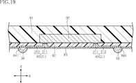
- FIG. 1 It is a top view of the semiconductor device which concerns on 1st Embodiment, and is transmitted through a sealing resin. It is a plan view corresponding to FIG. 1, and is further transmitted through a semiconductor element. It is a bottom view of the semiconductor device shown in FIG. 1. It is a bottom view corresponding to FIG. 3, and is transparent to a protective layer and a plurality of terminals. It is sectional drawing which follows the VV line of FIG. It is sectional drawing which follows the VI-VI line of FIG. It is a partially enlarged view of FIG. It is a partially enlarged view of FIG. FIG. 3 is a partially enlarged cross-sectional view taken along the line IX-IX of FIG. FIG. 7 is a partially enlarged view of FIG. 7.
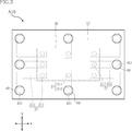
- FIG. 21 is a bottom view of the semiconductor device shown in FIG. It is a bottom view corresponding to FIG. 23, and is transparent to a protective layer and a plurality of terminals.
- 22 is a cross-sectional view taken along the line XXV-XXV of FIG. 22. 22 is a cross-sectional view taken along the line XXVI-XXVI of FIG. 22.
- FIG. 26 is a partially enlarged view. 22 is a partially enlarged cross-sectional view taken along the line XXVIII-XVIII of FIG. 22.
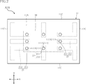
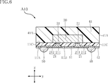
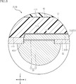
- the semiconductor device A10 includes a first insulating layer 11, a plurality of first wiring layers 21, a semiconductor element 30, a sealing resin 41, a protective layer 42, and a plurality of terminals 50.
- the semiconductor device A10 is surface-mounted on a wiring board.
- the semiconductor device A10 includes a single semiconductor element 30.
- the semiconductor device A10 may include a plurality of semiconductor elements 30.
- the plurality of semiconductor elements 30 include a laser diode and a switching element such as a MOSFET. In this configuration, when the switching element is driven, the laser diode emits light in a pulse shape at intervals of several ns.
- FIG. 1 the sealing resin 41 is transmitted, and in FIG. 2, the semiconductor element 30 is further transmitted with respect to FIG. In FIG. 4, the protective layer 42 and the plurality of terminals 50 are transmitted through.
- FIG. 2 the outer shape of the semiconductor element 30 is shown by an imaginary line (dashed-dotted line).
- the three directions orthogonal to each other are appropriately referred to.
- these are the first direction x, the second direction y, and the thickness direction z, but the present disclosure is not limited thereto.
- the thickness direction z corresponds to, for example, a direction penetrating the thickness of the first insulating layer 11.
- the outer shape of the semiconductor device A10 is rectangular when viewed along the thickness direction z.
- the first direction x is parallel to one side (first side) of the semiconductor device A10
- the second direction y is parallel to another side (second side orthogonal to the first side) of the semiconductor device A10.
- the first side is longer than the second side, but the present disclosure is not limited to this.
- the first insulating layer 11 faces the semiconductor element 30 in the thickness direction z.
- the first insulating layer 11 contains a thermosetting synthetic resin and an additive containing a metal element constituting a part of each of the plurality of first wiring layers 21 (first base layer 21A described later). It consists of materials.
- the synthetic resin is, for example, an epoxy resin or a polyimide.
- the first insulating layer 11 has a first main surface 11A, a first back surface 11B, and a plurality of end surfaces 11C.
- the first main surface 11A and the first back surface 11B face each other in the thickness direction z. Of these, the first main surface 11A faces the semiconductor element 30.
- the plurality of end faces 11C are connected to the first main surface 11A and the first back surface 11B.
- Each of the plurality of end faces 11C faces either the first direction x or the second direction y.
- the first insulating layer 11 has a plurality of first penetration portions 111.
- Each of the plurality of first penetrating portions 111 extends from the side where the first main surface 11A is located to the side where the first back surface 11B is located in the thickness direction z, and penetrates the first insulating layer 11 in the thickness direction z. doing.
- Each of the plurality of first penetration portions 111 is defined by any one of the plurality of first inner peripheral surfaces 111A of the first insulating layer 11.
- Each of the plurality of first inner peripheral surfaces 111A is inclined with respect to the first main surface 11A.
- Each of the plurality of first inner peripheral surfaces 111A has a plurality of first surfaces defined by the first inner peripheral surface 111A from the side where the first back surface 11B is located to the side where the first main surface 11A is located in the thickness direction z. Take a posture of falling toward one of the penetrating portions 111. Therefore, the cross-sectional area of each of the plurality of first penetrating portions 111 with respect to the thickness direction z gradually increases from the side where the first main surface 11A is located to the side where the first back surface 11B is located.
- the first insulating layer 11 has a plurality of first groove portions 112.
- Each of the plurality of first groove portions 112 is recessed from the first back surface 11B in the thickness direction z.
- Each of the plurality of first groove portions 112 is connected to any of the plurality of first penetration portions 111.
- each of the plurality of first groove portions 112 extends along a direction orthogonal to the thickness direction z.
- each pair of side surfaces of the plurality of first groove portions 112 is inclined with respect to the first back surface 11B.
- the width b1 of the first groove portion 112 at the boundary between the pair of side surfaces and the bottom surface of the first groove portion 112 is the boundary between the pair of side surfaces and the first back surface 11B. It is smaller than the width b2 of the first groove portion 112 in the above.
- the plurality of first wiring layers 21 are arranged in the first insulating layer 11 as shown in FIGS. 5 and 6.
- the plurality of first wiring layers 21 form a part of the conductive path between the wiring board on which the semiconductor device A10 is mounted and the semiconductor element 30.
- Each of the plurality of first wiring layers 21 includes a first communication unit 211 and a first main unit 212.
- the first connecting portion 211 is housed in one of a plurality of first penetrating portions 111 of the first insulating layer 11.
- the first connecting portion 211 is in contact with any of a plurality of first inner peripheral surfaces 111A defining the first penetrating portion 111.
- the first communication unit 211 is connected to one of a plurality of electrodes 31 (details will be described later) of the semiconductor element 30.
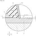
- the first main portion 212 is connected to the first communication portion 211 of any one of the plurality of first wiring layers 21, and the first back surface 11B is located in the first insulating layer 11. It is placed on the side. More specifically, the first main portion 212 is arranged in any of the plurality of first groove portions 112 of the first insulating layer 11. The first main portion 212 is in contact with the first groove portion 112. As shown in FIGS. 7 to 9, in the semiconductor device A10, a part of the first main portion 212 of each of the plurality of first wiring layers 21 protrudes from any of the plurality of first groove portions 112.
- each of the first connecting portion 211 and the first main portion 212 of the plurality of first wiring layers 21 has a first base layer 21A and a first plating layer 21B.
- the first base layer 21A is composed of a metal element contained in the additive contained in the first insulating layer 11.
- the first base layer 21A is in contact with the first insulating layer 11.
- Each of the plurality of first inner peripheral surfaces 111A of the first insulating layer 11 is covered with a first base layer 21A forming the first connecting portion 211 of any one of the plurality of first wiring layers 21.
- the first plating layer 21B covers the first base layer 21A of any one of the plurality of first wiring layers 21.
- the first plating layer 21B is made of a material containing, for example, copper (Cu). As shown in FIG. 9, the first plating layer 21B of each of the first main portions 212 of the plurality of first wiring layers 21 has a recess 212A recessed in the thickness direction z. The recess 212A extends along the direction in which any of the plurality of first groove portions 112 of the first insulating layer 11 extends.
- the semiconductor element 30 is arranged in contact with the first main surface 11A of the first insulating layer 11.
- the semiconductor element 30 is a flip chip mounting type.
- the semiconductor device 30 has a plurality of electrodes 31.
- the plurality of electrodes 31 are provided on either side of the thickness direction z in the semiconductor element 30.
- the plurality of electrodes 31 are provided on the side closer to the first main surface 11A in the thickness direction z.
- Each of the plurality of electrodes 31 is conducting to the circuit configured in the semiconductor element 30.
- Each of the plurality of electrodes 31 is composed of a single metal layer or a plurality of metal layers laminated in the thickness direction z. As shown in FIG.
- each of the plurality of electrodes 31 has a connecting surface 311.
- the connection surface 311 faces the same side as the first back surface 11B of the first insulating layer 11 in the thickness direction z.
- Each of the first communication portions 211 of the plurality of first wiring layers 21 is connected to the connection surface 311 of any one of the plurality of electrodes 31.
- the semiconductor element 30 is conductive to the plurality of first wiring layers 21.
- the semiconductor element 30 has a passivation film 32.
- the passivation film 32 is in contact with the first main surface 11A in the semiconductor element 30.
- the passivation film 32 is in contact with each of the plurality of electrodes 31.
- the passivation film 32 is made of a material containing, for example, polyimide.
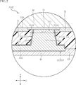
- each connection surface 311 of the plurality of electrodes 31 has a first region 311A and a second region 311B.
- the first region 311A is exposed from the first insulating layer 11 by any of the plurality of first penetrating portions 111 of the first insulating layer 11.
- the first plating layer 21B of the first connecting portion 211 is in contact with the first region 311A of any of the plurality of electrodes 31.
- the second region 311B is covered with the first insulating layer 11. As shown in FIG.
- the surface roughness sr1 of the first region 311A is larger than the surface roughness sr2 of the second region 311B.
- the surface roughness sr1 and sr2 are the bottommost portion of each connection surface 311 of the plurality of electrodes 31 located inward of the electrode 31 in the thickness direction z, and the thickness direction from the bottommost portion. It is the distance in the thickness direction z from the highest portion located farthest in z.
- the sealing resin 41 is arranged in contact with the first main surface 11A of the first insulating layer 11 and covers a part of the semiconductor element 30.
- the sealing resin 41 is made of a material containing, for example, a black epoxy resin.
- the sealing resin 41 has a plurality of side surfaces 41A. Each of the plurality of side surfaces 41A faces either the first direction x or the second direction y. Each of the plurality of side surfaces 41A is flush with any of the plurality of end faces 11C of the first insulating layer 11.
- the protective layer 42 covers the first back surface 11B of the first insulating layer 11 and the first main portion 212 of the plurality of first wiring layers 21.
- the protective layer 42 faces the wiring board.
- the protective layer 42 has electrical insulation.
- the protective layer 42 is made of, for example, a material containing polyimide.
- the protective layer 42 has a plurality of openings 421. The plurality of openings 421 penetrate the protective layer 42 in the thickness direction z. A part of the first main portion 212 of each of the plurality of first wiring layers 21 is exposed from the protective layer 42 by any of the plurality of openings 421.
- the plurality of terminals 50 are individually bonded to a part of the first main portion 212 of the plurality of first wiring layers 21 exposed from the plurality of openings 421 of the protective layer 42. ing.
- the plurality of terminals 50 are used for mounting the semiconductor device A10 on the wiring board.
- the plurality of terminals 50 project from the protective layer 42 in the thickness direction z.
- each of the plurality of terminals 50 has a base portion 51 and a bump portion 52.
- the base 51 is in contact with any part of the first main portion 212 of the plurality of first wiring layers 21.
- the base 51 is a plurality of metal layers in which a nickel (Ni) layer, a palladium layer (Pd), and a gold (Au) layer are laminated in this order in a direction away from the first back surface 11B of the first insulating layer 11 in the thickness direction z. Consists of. Here, among these metal layers, the palladium layer may not be provided.
- the bump portion 52 is in contact with both the base portion 51 and the protective layer 42.
- the bump portion 52 includes a portion protruding from the protective layer 42 in the thickness direction z.
- the bump portion 52 is made of a material containing tin (Sn).
- the bump portion 52 is made of, for example, lead-free solder.
- FIGS. 11 to 20 An example of a method for manufacturing the semiconductor device A10 will be described with reference to FIGS. 11 to 20.
- the cross-sectional positions of FIGS. 11 to 20 (excluding FIGS. 14, 15 and 17) are the same as the cross-sectional positions of FIG.
- the semiconductor element 30 is embedded in the sealing resin 81.
- the sealing resin 81 is made of a material containing a black epoxy resin.
- compression molding is performed.
- the semiconductor element 30 is embedded in the sealing resin 81.
- the plurality of electrodes 31 are exposed from the sealing resin 81.
- an insulating layer 82 is formed, which is laminated on the sealing resin 81 and covers a plurality of electrodes 31 of the semiconductor element 30.
- the insulating layer 82 is made of a material containing a thermosetting synthetic resin and an additive containing a metal element constituting a part of a plurality of wiring layers 83 (details will be described later).
- the synthetic resin is an epoxy resin or a polyimide.
- the insulating layer 82 is formed by compression molding.
- each of the plurality of wiring layers 83 includes a first communication unit 211 and a first main unit 212.
- the step of forming the plurality of wiring layers 83 includes a step of precipitating the base layer 83A on the insulating layer 82 and a step of forming a plating layer 83B covering the base layer 83A.
- the base layer 83A is deposited on the insulating layer 82.
- the base layer 83A is composed of the metal element contained in the additive contained in the insulating layer 82.
- a plurality of through portions 821 and a plurality of groove portions 822 are formed in the insulating layer 82.
- the plurality of penetrating portions 821 penetrate the insulating layer 82 in the thickness direction z. Each of the plurality of penetration portions 821 exposes a part of the surface (connection surface 311) of any of the plurality of electrodes 31 of the semiconductor element 30 from the insulating layer 82.
- Each of the plurality of groove portions 822 is recessed from the surface 82A of the insulating layer 82 and is connected to any of the plurality of through portions 821.
- the front surface 82A corresponds to the first back surface 11B of the first insulating layer 11.
- the plurality of penetration portions 821 and the plurality of groove portions 822 are formed by irradiating the insulating layer 82 with a laser while recognizing the positions of the plurality of electrodes 31 with an infrared camera.
- the laser irradiation position on the insulating layer 82 is corrected one by one based on the position information of the plurality of electrodes 31 obtained by image recognition.
- the laser is an ultraviolet laser having a wavelength of 355 nm and a beam diameter of 17 ⁇ m.
- Concavo-convex 31A is formed in one region 311A) by laser irradiation.
- the metal element contained in the additive contained in the insulating layer 82 is excited.
- a base layer 83A that covers the inner peripheral surface 821A of the insulating layer 82 that individually defines the plurality of penetrating portions 821 and the plurality of groove portions 822 is formed.
- a plating layer 83B covering the base layer 83A is formed.
- the plating layer 83B is made of a material containing copper.
- the plating layer 83B is formed by electroless plating, electrolytic plating, or a combination thereof.
- each of the plurality of penetration portions 821 is formed with the first communication portion 211 of any of the plurality of wiring layers 83.
- each of the plurality of groove portions 822 is formed with the first main portion 212 of any one of the plurality of wiring layers 83.
- the plurality of wiring layers 83 are formed.
- a protective layer 84 is formed which is laminated on the insulating layer 82 and covers the first main portion 212 of the plurality of wiring layers 83.
- the protective layer 84 has a plurality of openings 841 penetrating in the thickness direction z.
- the photosensitive polyimide is applied to the surface of the insulating layer 82 and the surfaces of the plurality of wiring layers 83 using a spin coater.
- a plurality of openings 841 are formed in the photosensitive polyimide by photolithography patterning. As a result, a part of the first main portion 212 of each of the plurality of wiring layers 83 is exposed from the protective layer 84 by any of the plurality of openings 841.
- a plurality of terminals 50 individually bonded to a part of the first main portion 212 of the plurality of wiring layers 83 exposed by the plurality of openings 841 of the protective layer 84 are formed.
- the base 51 of the plurality of terminals 50 shown in FIG. 8 is formed.
- the base 51 is formed by electroless plating.
- the bump portions 52 of the plurality of terminals 50 shown in FIG. 8 are formed.
- the bump portion 52 is formed by melting a conductive material containing tin such as lead-free solder by reflow and then solidifying it by cooling. As a result, a plurality of terminals 50 are formed.
- the sealing resin 81, the insulating layer 82, and the protective layer 84 are cut into a plurality of pieces by cutting along the cutting line CL with a dicing blade or the like.
- the individual piece includes one semiconductor element 30 and a plurality of wiring layers 83 connected to the semiconductor element 30.
- the sealing resin 81, the insulating layer 82, and the protective layer 84, which are individually formed by this step, correspond to the sealing resin 41, the first insulating layer 11, and the protective layer 42 of the semiconductor device A10. Through the above steps, the semiconductor device A10 is manufactured.
- the first connecting portion 211 of the first wiring layer 21 of the semiconductor device A10 is housed in the first penetrating portion 111 of the first insulating layer 11 and is connected to the electrode 31 of the semiconductor element 30.
- the electrode 31 has a connecting surface 311 including a first region 311A and a second region 311B.
- the first region 311A is exposed from the first insulating layer 11 at the first penetrating portion 111.
- the second region 311B is covered with the first insulating layer 11.
- the first communication unit 211 is in contact with the first region 311A. As shown in FIG. 10, the surface roughness sr1 of the first region 311A is larger than the surface roughness sr2 of the second region 311B.
- the surface area per unit area of the first region 311A becomes larger than the surface area per unit area of the second region 311B. Therefore, the contact area of the first contact portion 211 with respect to the first region 311A increases. Further, the anchoring effect (anchor effect) of the first communication unit 211 with respect to the first region 311A is exhibited. Therefore, according to the semiconductor device A10, it is possible to further improve the adhesion of the wiring layer (first wiring layer 21) to the electrode 31 of the semiconductor element 30.
- the step of forming the wiring layer 83 according to the manufacturing method of the semiconductor device A10 includes a step of precipitating the base layer 83A on the insulating layer 82.
- the through portion 821 that exposes a part of the surface (connection surface 311) of the electrode 31 of the semiconductor element 30 from the insulating layer 82 is formed by laser irradiation, so that the inside of the insulating layer 82 that defines the through portion 821 is formed.
- the base layer 83A covering the peripheral surface 821A is deposited.
- the laser forms unevenness 31A on a part of the surface of the electrode 31 exposed from the insulating layer 82 at the penetrating portion 821.
- the surface of the electrode 31, that is, the connection surface 311 of the electrode 31 can be configured to include the first region 311A and the second region 311B.
- the penetrating portion 821 is formed on the insulating layer 82, the insulating layer 82 is irradiated with the laser while recognizing the position of the electrode 31 as an image.
- the first region 311A and the second region 311B are configured to be accurately separated on the surface of the electrode 31 (connection surface 311).
- the first inner peripheral surface 111A defining the first penetrating portion 111 of the first insulating layer 11 is the first lower surface by including the step of precipitating the base layer 83A on the insulating layer 82. It will be covered with the stratum 21A.
- the first inner peripheral surface 111A is inclined with respect to the first main surface 11A of the first insulating layer 11. Further, the cross-sectional area of the first penetrating portion 111 with respect to the thickness direction z gradually increases from the side where the first main surface 11A is located to the side where the first back surface 11B is located. This is a configuration obtained by irradiating a laser from the surface 82A of the insulating layer 82 toward the surface (connecting surface 311) of the electrode 31 when the penetrating portion 821 is formed in the insulating layer 82.
- a groove portion 822 that is recessed from the surface 82A of the insulating layer 82 and is connected to the penetrating portion 821 is formed in the insulating layer 82 by laser irradiation.
- the base layer 83A covering the groove portion 822 is deposited. Therefore, the patterning of the wiring layer 83 can be freely performed by laser irradiation.
- the step of forming the wiring layer 83 according to the manufacturing method of the semiconductor device A10 includes a step of forming a plating layer 83B covering the base layer 83A.
- the plating layer 83B is formed by electroless plating, electrolytic plating, or a combination thereof.
- the forming method by electroless plating provides a conductive path necessary for performing the electrolytic plating on the surface 82A of the insulating layer 82 as compared with the forming method by electroplating. Is unnecessary. Therefore, the wiring layer 83 can be formed more efficiently.
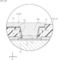
- the semiconductor device A10 includes a protective layer 42 and terminals 50.
- the protective layer 42 covers the first back surface 11B of the first insulating layer 11 and the first main portion 212 of the first wiring layer 21.
- the protective layer 42 has an opening 421 in which a part of the first main portion 212 is exposed from the protective layer 42.
- the terminal 50 is joined to a part of the first main portion 212 exposed from the protective layer 42 at the opening 421, and protrudes from the protective layer 42 in the thickness direction.
- the terminal 50 made of a material containing tin, when the semiconductor device A10 is mounted on the wiring board, at least a part of the terminal 50 is melted by the reflow. As a result, the effect of self-repairing the positional deviation of the semiconductor device A10 with respect to the wiring board (self-alignment effect) can be obtained.
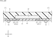
- the semiconductor device A20 according to the second embodiment will be described with reference to FIGS. 21 to 28.
- the same or similar elements as the above-mentioned semiconductor device A10 are designated by the same reference numerals, and duplicate description will be omitted.
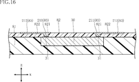
- the semiconductor device A20 further includes the second insulating layer 12 and the plurality of second wiring layers 22, and the configuration of the protective layer 42 and the plurality of terminals 50 is different from that of the semiconductor device A10.
- the sealing resin 41 is transmitted, and in FIG. 22, the first insulating layer 11 and the semiconductor element 30 are further transmitted with respect to FIG. 21.
- the protective layer 42 and the plurality of terminals 50 are transmitted through.
- the outer shape of the transmitted semiconductor element 30 is shown by an imaginary line.
- the second insulating layer 12 is arranged in contact with the first back surface 11B of the first insulating layer 11.
- the first insulating layer 11 has a structure sandwiched between the second insulating layer 12 and the sealing resin 41 in the thickness direction z.
- the second insulating layer 12 contains a thermosetting synthetic resin and an additive containing a metal element constituting a part of each of the plurality of second wiring layers 22 (second base layer 22A described later). It consists of materials.
- the synthetic resin is, for example, an epoxy resin or a polyimide.
- the second insulating layer 12 has a second main surface 12A, a second back surface 12B, and a plurality of end surfaces 12C.
- the second main surface 12A and the second back surface 12B face opposite to each other in the thickness direction z. Of these, the second main surface 12A is in contact with the first back surface 11B.
- the plurality of end faces 12C are connected to the second main surface 12A and the second back surface 12B. Each of the plurality of end faces 12C faces either the first direction x or the second direction y. Each of the plurality of end faces 12C is flush with both of the plurality of end faces 11C of the first insulating layer 11 and any of the plurality of side surfaces 41A of the sealing resin 41.
- the second insulating layer 12 has a plurality of second penetration portions 121.
- Each of the plurality of second penetrating portions 121 extends from the side where the second main surface 12A is located to the side where the second back surface 12B is located in the thickness direction z, and penetrates the second insulating layer 12 in the thickness direction z. doing.
- Each of the plurality of second penetration portions 121 is defined by any one of the plurality of second inner peripheral surfaces 121A of the second insulating layer 12.
- Each of the plurality of second inner peripheral surfaces 121A is inclined with respect to the second main surface 12A.
- Each of the plurality of second inner peripheral surfaces 121A has a plurality of second surfaces defined by the second inner peripheral surface 121A from the side where the second back surface 12B is located to the side where the second main surface 12A is located in the thickness direction z. Take a posture of falling toward any of the penetrating portions 121. Therefore, the cross-sectional area of each of the plurality of second penetrating portions 121 with respect to the thickness direction z gradually increases from the side where the second main surface 12A is located to the side where the second back surface 12B is located.
- the second insulating layer 12 has a plurality of second groove portions 122.
- Each of the plurality of second groove portions 122 is recessed from the second back surface 12B in the thickness direction z.
- Each of the plurality of second groove portions 122 is connected to any of the plurality of second through portions 121.
- each of the plurality of second groove portions 122 extends along a direction orthogonal to the thickness direction z.
- each pair of side surfaces of the plurality of second groove portions 122 is inclined with respect to the second back surface 12B.
- the width b3 of the second groove portion 122 at the boundary between the pair of side surfaces and the bottom surface of the second groove portion 122 is the boundary between the pair of side surfaces and the second back surface 12B. It is smaller than the width b4 of the second groove portion 122 in the above.
- the plurality of second wiring layers 22 are arranged in the second insulating layer 12.
- the plurality of second wiring layers 22 together with the plurality of first wiring layers 21 form a part of the conductive path between the wiring board on which the semiconductor device A10 is mounted and the semiconductor element 30.
- Each of the plurality of second wiring layers 22 includes a second communication unit 221 and a second main unit 222.
- the second connecting portion 221 is housed in one of a plurality of second penetrating portions 121 of the second insulating layer 12.
- the second communication unit 221 is in contact with any of the plurality of second inner peripheral surfaces 121A defining the second penetration portion 121.
- the second communication unit 221 is connected to the first main unit 212 of any one of the plurality of first wiring layers 21.
- the second main portion 222 is connected to the second connecting portion 221 of any one of the plurality of second wiring layers 22, and the second back surface 12B is located in the second insulating layer 12. It is placed on the side. More specifically, the second main portion 222 is arranged in any of the plurality of second groove portions 122 of the second insulating layer 12. The second main portion 222 is in contact with the second groove portion 122.
- FIGS. 27 and 28 in the semiconductor device A20, a part of the second main portion 222 of each of the plurality of second wiring layers 22 protrudes from any of the plurality of second groove portions 122.
- each of the plurality of second penetration portions 121 of the second insulating layer 12 is any of the plurality of first wiring layers 21. It overlaps with the first main part 212.
- the second main portion 222 of each of the plurality of second wiring layers 22 is the first main portion 212 of any one of the plurality of first wiring layers 21.
- the first main portion 212 extends in a direction different from the extending direction.
- each of the second connecting portion 221 and the second main portion 222 of the plurality of second wiring layers 22 has a second base layer 22A and a second plating layer 22B.
- the second base layer 22A is composed of the metal element contained in the additive contained in the second insulating layer 12.
- the second base layer 22A is in contact with the second insulating layer 12.
- Each of the plurality of second inner peripheral surfaces 121A of the second insulating layer 12 is covered with a second base layer 22A forming the second connecting portion 221 of any of the plurality of second wiring layers 22.
- the second plating layer 22B covers the second base layer 22A of any one of the plurality of second wiring layers 22.
- the second plating layer 22B is made of, for example, a material containing copper.
- the second plating layer 22B is in contact with the first main portion 212 of any one of the plurality of first wiring layers 21.
- the second plating layer 22B of each of the second main portions 222 of the plurality of second wiring layers 22 has a recess 222A recessed in the thickness direction z.
- the recess 222A extends along a direction in which any of the plurality of second groove portions 122 of the second insulating layer 12 extends.
- the protective layer 42 covers the second back surface 12B of the second insulating layer 12 and the second main portion 222 of the plurality of second wiring layers 22.
- the protective layer 42 faces the wiring board.
- a part of the second main portion 222 of each of the plurality of second wiring layers 22 is exposed from the protective layer 42 by any of the plurality of openings 421.
- the plurality of terminals 50 are individually joined to a part of the second main portion 222 of the plurality of second wiring layers 22 exposed from the plurality of openings 421.
- the first connecting portion 211 of the first wiring layer 21 of the semiconductor device A20 is housed in the first penetrating portion 111 of the first insulating layer 11 and is connected to the electrode 31 of the semiconductor element 30.
- the electrode 31 has a connecting surface 311 including a first region 311A and a second region 311B.
- the first region 311A is exposed from the first insulating layer 11 at the first penetrating portion 111.
- the second region 311B is covered with the first insulating layer 11.
- the first communication unit 211 is in contact with the first region 311A.
- the surface roughness sr1 of the first region 311A is larger than the surface roughness sr2 of the second region 311B. Therefore, the semiconductor device A20 can also further improve the adhesion of the wiring layer (first wiring layer 21) to the electrode 31 of the semiconductor element 30.
- the semiconductor device A20 has a second insulating layer 12 having a second main surface 12A, a second back surface 12B, and a second penetrating portion 121, and a second wiring layer 22 having a second connecting portion 221 and a second main portion 222. Further prepare.
- the second main surface 12A is in contact with the first back surface 11B of the first insulating layer 11.
- the second connecting portion 221 is housed in the second penetrating portion 121 and is connected to the first main portion 212 of the first wiring layer 21.
- the second main portion 222 is connected to the second connecting portion 221 and is arranged on the side of the second insulating layer 12 where the second back surface 12B is located.
- the first main portion 212 is covered with the second insulating layer 12.
- the semiconductor device A20 When viewed along the thickness direction z, at least a part of the second penetrating portion 121 overlaps with the first main portion 212. As a result, in the semiconductor device A20, the second main portion 222 becomes the first main portion 222 when viewed along the thickness direction z without causing a short circuit in the conduction path between the first wiring layer 21 and the second wiring layer 22. It is possible to take an arrangement form that overlaps with the portion 212. Therefore, according to the semiconductor device A20, a conduction path more complicated than that of the semiconductor device A10 can be configured.
- the present disclosure is not limited to the above-described embodiment, and the specific configuration of each part of the semiconductor device can be freely redesigned. ..
- the configuration may include a plurality of semiconductor elements 30.
- the type of each semiconductor element 30 can be selected according to the required application and function.
- various components having a rectangular outer shape as viewed along the thickness direction z are used, but the present disclosure is not limited to this, and the outer shape is, for example, a circular shape or a hexagonal shape. And so on.
Abstract
A semiconductor device is provided with an insulation layer, a semiconductor element, a wiring layer, and a sealing resin. The insulation layer has a main surface and a reverse surface set away from each other in the thickness direction, and has formed therein a penetration part extending in the thickness direction. The semiconductor element has an electrode corresponding to the penetration part and is in contact with the main surface. The wiring part includes a linking part that is housed in the penetration part and is in contact with the electrode, and a main part that is continuous from the linking part and that is positioned on the reverse surface. The sealing resin is in contact with the main surface and covers the semiconductor element. The electrode has a connection surface facing the linking part. The connection surface includes a first region that is exposed from the insulation layer by the penetration part, and a second region in contact with the insulation layer. The surface roughness of the first region is higher than the surface roughness of the second region.
Description
本開示は、半導体装置と、当該半導体装置の製造方法とに関する。
This disclosure relates to a semiconductor device and a method for manufacturing the semiconductor device.
近年における電子機器の小型化に伴い、当該電子機器に用いられる半導体装置の小型化が進められている。こうした動向を受け、封止樹脂と、当該封止樹脂に積層された絶縁層と、当該絶縁層から露出する電極を有するとともに、当該封止樹脂および当該絶縁層に覆われた半導体素子と、当該電極につながり、かつ当該絶縁層に配置された配線層とを備える半導体装置が知られている。当該半導体装置がこのような構成をとることにより、当該装置の小型化を図ることができる。さらに、当該半導体装置の配線層は自在に設けることが可能であるため、当該装置は、実装対象となる配線基板の配線パターンに対して柔軟に対応できるという利点を有する。
With the miniaturization of electronic devices in recent years, the miniaturization of semiconductor devices used in the electronic devices is being promoted. In response to these trends, the encapsulating resin, the insulating layer laminated on the encapsulating resin, the electrodes exposed from the insulating layer, the encapsulating resin, and the semiconductor element covered with the insulating layer, and the said. A semiconductor device connected to an electrode and provided with a wiring layer arranged in the insulating layer is known. By adopting such a configuration in the semiconductor device, the size of the device can be reduced. Further, since the wiring layer of the semiconductor device can be freely provided, the device has an advantage that it can flexibly correspond to the wiring pattern of the wiring board to be mounted.
特許文献1には、このような半導体装置の製造方法の一例が開示されている。当該製造方法は、電極を有する半導体素子を封止樹脂(特許文献1では硬化体)に埋め込む工程と、当該半導体素子および当該封止樹脂に接する絶縁層(特許文献1ではバッファーコート膜)を形成する工程と、当該電極につながる配線層を形成する工程とを含む。半導体素子を封止樹脂に埋め込む工程では、電極が封止樹脂から露出するようにする。絶縁層を形成する工程では、フォトリソグラフィパターニングによって当該絶縁層に開口を形成する。絶縁層に形成された開口から電極が露出する。配線層を形成する工程では、電極につながり、かつ開口に収容される部分を含むめっき層を形成する。めっき層は、配線層を構成する一要素である。
Patent Document 1 discloses an example of a method for manufacturing such a semiconductor device. In the manufacturing method, a step of embedding a semiconductor element having an electrode in a sealing resin (cured body in Patent Document 1) and an insulating layer (buffer coat film in Patent Document 1) in contact with the semiconductor element and the sealing resin are formed. A step of forming a wiring layer connected to the electrode is included. In the process of embedding the semiconductor element in the encapsulating resin, the electrodes are exposed from the encapsulating resin. In the step of forming the insulating layer, an opening is formed in the insulating layer by photolithography patterning. The electrodes are exposed from the openings formed in the insulating layer. In the step of forming the wiring layer, a plating layer including a portion connected to the electrode and accommodated in the opening is formed. The plating layer is one element constituting the wiring layer.
配線層を形成する工程では、半導体素子の電極と、当該電極につながる配線層との間に空隙が発生することがある。空隙の発生規模が比較的大きくなると、半導体素子と配線層との導通が阻害されるおそれがある。したがって、電極に対する配線層の密着性をより向上させることよって、空隙の発生規模を抑制することが望まれる。
In the process of forming the wiring layer, a gap may be generated between the electrode of the semiconductor element and the wiring layer connected to the electrode. If the scale of void generation is relatively large, the conduction between the semiconductor element and the wiring layer may be hindered. Therefore, it is desired to suppress the scale of void generation by further improving the adhesion of the wiring layer to the electrodes.
本開示は上述の事情に鑑み、半導体素子の電極に対する配線層の密着性をより向上させることが可能な半導体装置およびその製造方法を提供することをその課題とする。
In view of the above circumstances, it is an object of the present disclosure to provide a semiconductor device capable of further improving the adhesion of the wiring layer to the electrodes of the semiconductor element and a method for manufacturing the same.
本開示の第1の側面によれば、半導体装置が提供される。当該半導体装置は、厚さ方向において互いに離間する第1主面および第1裏面を有し、前記厚さ方向に延びる第1貫通部が形成された第1絶縁層と;前記第1貫通部に対応する電極を有し、前記第1主面に接する半導体素子と;前記第1貫通部に収容され且つ前記電極に接する第1連絡部と、前記第1連絡部につながり且つ前記第1裏面に配置された第1主部と、を含む第1配線層と;前記第1主面に接し且つ前記半導体素子を覆う封止樹脂と、を備える。前記電極は、前記第1連絡部に対向する接続面を有し、前記接続面は、前記第1貫通部により前記第1絶縁層から露出する第1領域と、前記第1絶縁層に接する第2領域と、を含む。前記第1領域の表面粗さは、前記第2領域の表面粗さよりも大である。
According to the first aspect of the present disclosure, a semiconductor device is provided. The semiconductor device has a first main surface and a first back surface that are separated from each other in the thickness direction, and a first insulating layer on which a first penetration portion extending in the thickness direction is formed; A semiconductor device having a corresponding electrode and in contact with the first main surface; a first contact portion housed in the first penetration portion and in contact with the electrode, and a first contact portion connected to the first contact portion and on the first back surface. A first wiring layer including an arranged first main portion; a sealing resin in contact with the first main surface and covering the semiconductor element. The electrode has a connecting surface facing the first connecting portion, and the connecting surface is in contact with a first region exposed from the first insulating layer by the first penetrating portion and the first insulating layer. Includes 2 regions. The surface roughness of the first region is larger than the surface roughness of the second region.
好ましくは、前記第1配線層は、前記第1絶縁層に接する第1下地層と、前記第1下地層を覆う第1めっき層と、を有し、前記第1めっき層が前記第1領域に接している。
Preferably, the first wiring layer has a first base layer in contact with the first insulating layer and a first plating layer covering the first base layer, and the first plating layer is the first region. Is in contact with.
好ましくは、前記第1絶縁層は、熱硬化性の合成樹脂と、前記第1下地層を組成する金属元素が含有された添加剤と、を含む材料からなる。
Preferably, the first insulating layer is made of a material containing a thermosetting synthetic resin and an additive containing a metal element constituting the first base layer.
好ましくは、前記第1絶縁層は、前記第1裏面から凹み且つ前記第1貫通部につながる溝部を有し、前記第1主部は前記溝部に配置されている。
Preferably, the first insulating layer has a groove portion recessed from the first back surface and connected to the first penetrating portion, and the first main portion is arranged in the groove portion.
好ましくは、前記第1主部は、前記厚さ方向に向けて凹む凹部を有し、前記凹部は、前記溝部が延びる方向に沿って延びている。
Preferably, the first main portion has a recess recessed in the thickness direction, and the recess extends along the direction in which the groove portion extends.
好ましくは、前記第1絶縁層は、前記第1貫通部を規定する第1内周面を有し、前記第1内周面は、前記第1下地層に覆われ且つ前記第1主面に対して傾斜している。
Preferably, the first insulating layer has a first inner peripheral surface that defines the first penetrating portion, and the first inner peripheral surface is covered with the first base layer and is covered with the first main surface. On the other hand, it is inclined.
好ましくは、前記第1貫通部は、前記厚さ方向に直交する第1断面を有し、前記第1断面の面積は、前記第1主面から前記第1裏面に向かうほど大きくなる。
Preferably, the first penetration portion has a first cross section orthogonal to the thickness direction, and the area of the first cross section increases from the first main surface toward the first back surface.
好ましくは、前記半導体装置は、前記第1裏面および前記第1主部を覆う保護層をさらに備える。前記保護層は、前記厚さ方向に貫通する開口を有し、前記第1主部の一部が、前記開口で前記保護層から露出している。
Preferably, the semiconductor device further includes a protective layer that covers the first back surface and the first main portion. The protective layer has an opening penetrating in the thickness direction, and a part of the first main portion is exposed from the protective layer at the opening.
好ましくは、前記半導体装置は、端子をさらに備え、前記端子は、前記開口で前記保護層から露出する前記第1主部の一部に接合される。また前記端子は、前記保護層から前記厚さ方向に向けて突出している。
Preferably, the semiconductor device further comprises terminals, which are joined to a portion of the first main portion exposed from the protective layer at the opening. Further, the terminal protrudes from the protective layer in the thickness direction.
好ましくは、前記端子は、錫を含む材料からなる。
Preferably, the terminal is made of a material containing tin.
好ましくは、前記半導体装置は、前記厚さ方向において互いに離間する第2主面および第2裏面有し、前記厚さ方向に延びる第2貫通部が形成され、前記第2主面が前記第1裏面に接する第2絶縁層と;前記第2貫通部に収容され且つ前記第1主部につながる第2連絡部と、前記第2連絡部につながり且つ前記第2裏面に配置された第2主部と、を含む第2配線層と;をさらに備える。前記第1主部は、前記第2絶縁層に覆われている。前記厚さ方向に沿って視て、前記第2貫通部の少なくとも一部が、前記第1主部に重なっている。
Preferably, the semiconductor device has a second main surface and a second back surface that are separated from each other in the thickness direction, a second penetrating portion extending in the thickness direction is formed, and the second main surface is the first surface. A second insulating layer in contact with the back surface; a second contact portion housed in the second penetration portion and connected to the first main portion, and a second main unit connected to the second contact portion and arranged on the second back surface. A second wiring layer including a portion; The first main portion is covered with the second insulating layer. When viewed along the thickness direction, at least a part of the second penetrating portion overlaps with the first main portion.
好ましくは、前記厚さ方向に沿って視て、前記第2主部は、前記第1主部に重なる部分を含むとともに、前記第1主部が延びる方向とは異なる方向に沿って延びている。
Preferably, when viewed along the thickness direction, the second main portion includes a portion overlapping the first main portion and extends in a direction different from the direction in which the first main portion extends. ..
好ましくは、前記第2配線層は、前記第2絶縁層に接する第2下地層と、前記第2下地層を覆う第2めっき層と、を有する。前記第2連絡部において、前記第2めっき層が前記第1主部に接している。
Preferably, the second wiring layer has a second base layer in contact with the second insulating layer and a second plating layer covering the second base layer. In the second connecting portion, the second plating layer is in contact with the first main portion.
好ましくは、前記第2絶縁層は、熱硬化性の合成樹脂と、前記第2下地層を組成する金属元素が含有された添加剤と、を含む材料からなる。
Preferably, the second insulating layer is made of a material containing a thermosetting synthetic resin and an additive containing a metal element constituting the second base layer.
好ましくは、前記第2絶縁層は、前記第2貫通部を規定する第2内周面を有し、前記第2内周面は、前記第2下地層に覆われ且つ前記第2主面に対して傾斜している。
Preferably, the second insulating layer has a second inner peripheral surface that defines the second penetrating portion, and the second inner peripheral surface is covered with the second base layer and is covered with the second main surface. On the other hand, it is inclined.
好ましくは、前記第2貫通部は、前記厚さ方向に直交する第2断面を有し、前記第2断面の面積は、前記第2主面から前記第2裏面に向かうほど大きくなる。
Preferably, the second penetration portion has a second cross section orthogonal to the thickness direction, and the area of the second cross section increases from the second main surface toward the second back surface.
本開示の第2の側面によれば、半導体装置の製造方法が提供される。当該製造方法は、電極を有する半導体素子を、前記電極が露出するように封止樹脂に埋め込む工程と;前記封止樹脂の上に積層され且つ前記電極を覆う絶縁層を形成する工程と:前記絶縁層に埋め込まれ且つ前記電極につながる連絡部と、前記連絡部につながる主部と、を有する配線層を形成する工程と;を備える。前記絶縁層は、熱硬化性の合成樹脂と、前記配線層の一部を組成する金属元素が含有された添加剤と、を含む材料からなる。前記配線層を形成する工程は、(a)前記電極の表面の一部を前記絶縁層から露出させる貫通部と、前記絶縁層の表面から凹み且つ前記貫通部につながる溝部と、をレーザ照射により前記絶縁層に形成する工程と、(b)前記貫通部を規定する前記絶縁層の内周面と前記溝部とを覆い、かつ前記金属元素を含む下地層を前記絶縁層に析出させる工程と、(c)前記下地層を覆うめっき層を形成する工程と、を含む。前記下地層を析出させる工程は、前記レーザ照射により、前記貫通部で前記絶縁層から露出する前記電極の表面の一部に凹凸を形成することを含む。
According to the second aspect of the present disclosure, a method for manufacturing a semiconductor device is provided. The manufacturing method includes a step of embedding a semiconductor element having an electrode in a sealing resin so that the electrode is exposed; and a step of forming an insulating layer laminated on the sealing resin and covering the electrode. A step of forming a wiring layer having a connecting portion embedded in an insulating layer and connected to the electrode and a main portion connected to the connecting portion; The insulating layer is made of a material containing a thermosetting synthetic resin and an additive containing a metal element constituting a part of the wiring layer. In the step of forming the wiring layer, (a) a penetrating portion that exposes a part of the surface of the electrode from the insulating layer and a groove portion that is recessed from the surface of the insulating layer and connected to the penetrating portion are irradiated with a laser. A step of forming the insulating layer, and (b) a step of covering the inner peripheral surface of the insulating layer defining the penetrating portion and the groove portion and precipitating a base layer containing the metal element on the insulating layer. (C) The step of forming a plating layer covering the base layer is included. The step of precipitating the base layer includes forming irregularities on a part of the surface of the electrode exposed from the insulating layer at the penetrating portion by the laser irradiation.
好ましくは、前記めっき層を形成する工程は、無電解めっきまたは電解めっきの少なくとも一方によって前記めっき層を形成することを含む。
Preferably, the step of forming the plating layer includes forming the plating layer by at least one of electroless plating and electrolytic plating.
本開示にかかる半導体装置およびその製造方法によれば、半導体素子の電極に対する配線層の密着性をより向上させることが可能となる。
According to the semiconductor device and the manufacturing method thereof according to the present disclosure, it is possible to further improve the adhesion of the wiring layer to the electrodes of the semiconductor element.
本開示のその他の特徴および利点は、添付図面に基づき以下に行う詳細な説明によって、より明らかとなろう。
Other features and advantages of this disclosure will become more apparent with the detailed description given below based on the accompanying drawings.
本開示にかかる実施の形態について、添付図面に基づいて説明する。
An embodiment of the present disclosure will be described based on the attached drawings.
図1~図10に基づき、第1実施形態にかかる半導体装置A10について説明する。半導体装置A10は、第1絶縁層11、複数の第1配線層21、半導体素子30、封止樹脂41、保護層42、および複数の端子50を備える。半導体装置A10は、配線基板に表面実装される。半導体装置A10は、単一の半導体素子30を備える。これに代えて、半導体装置A10は、複数の半導体素子30を備えていてもよい。一例として、複数の半導体素子30は、レーザーダイオードと、MOSFETなどのスイッチング素子とを含む。この構成においては、スイッチング素子が駆動することにより、レーザーダイオードが数nsの間隔でパルス状に発光する。このような半導体装置A10を用いることにより、レーダと同じく、比較的遠距離に位置する対象の探査が可能となる。このような探査技術は、LIDAR(Laser Imaging Detection and Ranging)と称される。理解の便宜上、図1では、封止樹脂41を透過しており、図2では、図1に対して半導体素子30をさらに透過している。図4では、保護層42、および複数の端子50を透過している。図2においては、半導体素子30の外形を想像線(二点鎖線)で示している。
The semiconductor device A10 according to the first embodiment will be described with reference to FIGS. 1 to 10. The semiconductor device A10 includes a first insulating layer 11, a plurality of first wiring layers 21, a semiconductor element 30, a sealing resin 41, a protective layer 42, and a plurality of terminals 50. The semiconductor device A10 is surface-mounted on a wiring board. The semiconductor device A10 includes a single semiconductor element 30. Instead of this, the semiconductor device A10 may include a plurality of semiconductor elements 30. As an example, the plurality of semiconductor elements 30 include a laser diode and a switching element such as a MOSFET. In this configuration, when the switching element is driven, the laser diode emits light in a pulse shape at intervals of several ns. By using such a semiconductor device A10, it is possible to search for an object located at a relatively long distance like a radar. Such exploration technology is called LIDAR (Laser Imaging Detection and Ranging). For convenience of understanding, in FIG. 1, the sealing resin 41 is transmitted, and in FIG. 2, the semiconductor element 30 is further transmitted with respect to FIG. In FIG. 4, the protective layer 42 and the plurality of terminals 50 are transmitted through. In FIG. 2, the outer shape of the semiconductor element 30 is shown by an imaginary line (dashed-dotted line).
半導体装置A10に関する説明の便宜上、互いに直交する3つの方向を適宜参照する。図示の例では、これらは、第1方向x、第2方向y、および厚さ方向zであるが、本開示がこれに限定されるわけではない。図5等に示すように、厚さ方向zは、たとえば第1絶縁層11の厚みを貫通する方向に相当する。図1に示すように、半導体装置A10の外形は、厚さ方向zに沿って視て矩形状である。第1方向xは、半導体装置A10の一辺(第1辺)に平行であり、第2方向yは、半導体装置A10の別の辺(第1辺に直交する第2辺)に平行である。図示の例では、第1辺の方が第2辺より長いが、本開示がこれに限定されるわけではない。
For convenience of explanation regarding the semiconductor device A10, the three directions orthogonal to each other are appropriately referred to. In the illustrated example, these are the first direction x, the second direction y, and the thickness direction z, but the present disclosure is not limited thereto. As shown in FIG. 5 and the like, the thickness direction z corresponds to, for example, a direction penetrating the thickness of the first insulating layer 11. As shown in FIG. 1, the outer shape of the semiconductor device A10 is rectangular when viewed along the thickness direction z. The first direction x is parallel to one side (first side) of the semiconductor device A10, and the second direction y is parallel to another side (second side orthogonal to the first side) of the semiconductor device A10. In the illustrated example, the first side is longer than the second side, but the present disclosure is not limited to this.
図5および図6に示すように、第1絶縁層11は、厚さ方向zにおいて半導体素子30に対向している。第1絶縁層11は、熱硬化性の合成樹脂と、複数の第1配線層21の各々の一部(後述する第1下地層21A)を組成する金属元素が含有された添加剤とを含む材料からなる。当該合成樹脂は、たとえば、エポキシ樹脂、またはポリイミドである。第1絶縁層11は、第1主面11A、第1裏面11B、および複数の端面11Cを有する。第1主面11Aおよび第1裏面11Bは、厚さ方向zにおいて互いに反対側を向く。これらのうち第1主面11Aは、半導体素子30に対向している。複数の端面11Cは、第1主面11Aおよび第1裏面11Bにつながっている。複数の端面11Cの各々は、第1方向xおよび第2方向yのいずれかを向く。
As shown in FIGS. 5 and 6, the first insulating layer 11 faces the semiconductor element 30 in the thickness direction z. The first insulating layer 11 contains a thermosetting synthetic resin and an additive containing a metal element constituting a part of each of the plurality of first wiring layers 21 (first base layer 21A described later). It consists of materials. The synthetic resin is, for example, an epoxy resin or a polyimide. The first insulating layer 11 has a first main surface 11A, a first back surface 11B, and a plurality of end surfaces 11C. The first main surface 11A and the first back surface 11B face each other in the thickness direction z. Of these, the first main surface 11A faces the semiconductor element 30. The plurality of end faces 11C are connected to the first main surface 11A and the first back surface 11B. Each of the plurality of end faces 11C faces either the first direction x or the second direction y.
図2、図4および図7に示すように、第1絶縁層11は、複数の第1貫通部111を有する。複数の第1貫通部111の各々は、厚さ方向zにおいて第1主面11Aが位置する側から第1裏面11Bが位置する側に至るとともに、第1絶縁層11を厚さ方向zに貫通している。複数の第1貫通部111の各々は、第1絶縁層11の複数の第1内周面111Aのいずれかにより規定されている。複数の第1内周面111Aの各々は、第1主面11Aに対して傾斜している。複数の第1内周面111Aの各々は、厚さ方向zにおいて第1裏面11Bが位置する側から第1主面11Aが位置する側にかけて当該第1内周面111Aが規定する複数の第1貫通部111のいずれかに向けて倒れる姿勢をとる。したがって、複数の第1貫通部111の各々の厚さ方向zに対する横断面積は、第1主面11Aが位置する側から第1裏面11Bが位置する側に向かうほど、徐々に大きくなる。
As shown in FIGS. 2, 4 and 7, the first insulating layer 11 has a plurality of first penetration portions 111. Each of the plurality of first penetrating portions 111 extends from the side where the first main surface 11A is located to the side where the first back surface 11B is located in the thickness direction z, and penetrates the first insulating layer 11 in the thickness direction z. doing. Each of the plurality of first penetration portions 111 is defined by any one of the plurality of first inner peripheral surfaces 111A of the first insulating layer 11. Each of the plurality of first inner peripheral surfaces 111A is inclined with respect to the first main surface 11A. Each of the plurality of first inner peripheral surfaces 111A has a plurality of first surfaces defined by the first inner peripheral surface 111A from the side where the first back surface 11B is located to the side where the first main surface 11A is located in the thickness direction z. Take a posture of falling toward one of the penetrating portions 111. Therefore, the cross-sectional area of each of the plurality of first penetrating portions 111 with respect to the thickness direction z gradually increases from the side where the first main surface 11A is located to the side where the first back surface 11B is located.
図7~図9に示すように、第1絶縁層11は、複数の第1溝部112を有する。複数の第1溝部112の各々は、第1裏面11Bから厚さ方向zに向けて凹んでいる。複数の第1溝部112の各々は、複数の第1貫通部111のいずれかにつながっている。図4に示すように、複数の第1溝部112の各々は、厚さ方向zに対して直交する方向に沿って延びている。図9に示すように、複数の第1溝部112の各々の一対の側面は、第1裏面11Bに対して傾斜している。複数の第1溝部112の各々において、当該一対の側面と、当該第1溝部112の底面との境界における当該第1溝部112の幅b1は、当該一対の側面と、第1裏面11Bとの境界における当該第1溝部112の幅b2よりも小である。
As shown in FIGS. 7 to 9, the first insulating layer 11 has a plurality of first groove portions 112. Each of the plurality of first groove portions 112 is recessed from the first back surface 11B in the thickness direction z. Each of the plurality of first groove portions 112 is connected to any of the plurality of first penetration portions 111. As shown in FIG. 4, each of the plurality of first groove portions 112 extends along a direction orthogonal to the thickness direction z. As shown in FIG. 9, each pair of side surfaces of the plurality of first groove portions 112 is inclined with respect to the first back surface 11B. In each of the plurality of first groove portions 112, the width b1 of the first groove portion 112 at the boundary between the pair of side surfaces and the bottom surface of the first groove portion 112 is the boundary between the pair of side surfaces and the first back surface 11B. It is smaller than the width b2 of the first groove portion 112 in the above.
複数の第1配線層21は、図5および図6に示すように、第1絶縁層11に配置されている。複数の第1配線層21は、半導体装置A10が実装される配線基板と、半導体素子30との導電経路の一部をなしている。複数の第1配線層21の各々は、第1連絡部211および第1主部212を含む。図2、図4および図7に示すように、第1連絡部211は、第1絶縁層11の複数の第1貫通部111のいずれかに収容されている。第1連絡部211は、当該第1貫通部111を規定する複数の第1内周面111Aのいずれかに接している。第1連絡部211は、半導体素子30の複数の電極31(詳細は後述)のいずれかにつながっている。図4~図6に示すように、第1主部212は、複数の第1配線層21のいずれかの第1連絡部211につながり、かつ第1絶縁層11において第1裏面11Bが位置する側に配置されている。より具体的には、第1主部212は、第1絶縁層11の複数の第1溝部112のいずれかに配置されている。第1主部212は、当該第1溝部112に接している。図7~図9に示すように、半導体装置A10においては、複数の第1配線層21の各々の第1主部212の一部が、複数の第1溝部112のいずれかからはみ出している。
The plurality of first wiring layers 21 are arranged in the first insulating layer 11 as shown in FIGS. 5 and 6. The plurality of first wiring layers 21 form a part of the conductive path between the wiring board on which the semiconductor device A10 is mounted and the semiconductor element 30. Each of the plurality of first wiring layers 21 includes a first communication unit 211 and a first main unit 212. As shown in FIGS. 2, 4 and 7, the first connecting portion 211 is housed in one of a plurality of first penetrating portions 111 of the first insulating layer 11. The first connecting portion 211 is in contact with any of a plurality of first inner peripheral surfaces 111A defining the first penetrating portion 111. The first communication unit 211 is connected to one of a plurality of electrodes 31 (details will be described later) of the semiconductor element 30. As shown in FIGS. 4 to 6, the first main portion 212 is connected to the first communication portion 211 of any one of the plurality of first wiring layers 21, and the first back surface 11B is located in the first insulating layer 11. It is placed on the side. More specifically, the first main portion 212 is arranged in any of the plurality of first groove portions 112 of the first insulating layer 11. The first main portion 212 is in contact with the first groove portion 112. As shown in FIGS. 7 to 9, in the semiconductor device A10, a part of the first main portion 212 of each of the plurality of first wiring layers 21 protrudes from any of the plurality of first groove portions 112.
図7~図9に示すように、複数の第1配線層21の各々の第1連絡部211および第1主部212は、第1下地層21Aおよび第1めっき層21Bを有する。第1下地層21Aは、第1絶縁層11に含まれる添加剤に含有された金属元素により組成される。第1下地層21Aは、第1絶縁層11に接している。第1絶縁層11の複数の第1内周面111Aの各々は、複数の第1配線層21のいずれかの第1連絡部211をなす第1下地層21Aに覆われている。第1めっき層21Bは、複数の第1配線層21のいずれかの第1下地層21Aを覆っている。第1めっき層21Bは、たとえば銅(Cu)を含む材料からなる。図9に示すように、複数の第1配線層21の各々の第1主部212の第1めっき層21Bは、厚さ方向zに向けて凹む凹部212Aを有する。凹部212Aは、第1絶縁層11の複数の第1溝部112のいずれかが延びる方向に沿って延びている。
As shown in FIGS. 7 to 9, each of the first connecting portion 211 and the first main portion 212 of the plurality of first wiring layers 21 has a first base layer 21A and a first plating layer 21B. The first base layer 21A is composed of a metal element contained in the additive contained in the first insulating layer 11. The first base layer 21A is in contact with the first insulating layer 11. Each of the plurality of first inner peripheral surfaces 111A of the first insulating layer 11 is covered with a first base layer 21A forming the first connecting portion 211 of any one of the plurality of first wiring layers 21. The first plating layer 21B covers the first base layer 21A of any one of the plurality of first wiring layers 21. The first plating layer 21B is made of a material containing, for example, copper (Cu). As shown in FIG. 9, the first plating layer 21B of each of the first main portions 212 of the plurality of first wiring layers 21 has a recess 212A recessed in the thickness direction z. The recess 212A extends along the direction in which any of the plurality of first groove portions 112 of the first insulating layer 11 extends.
半導体素子30は、図5および図6に示すように、第1絶縁層11の第1主面11Aに接して配置されている。半導体装置A10においては、半導体素子30は、フリップチップ実装型である。半導体素子30は、複数の電極31を有する。複数の電極31は、半導体素子30において厚さ方向zのいずれかの側に設けられている。複数の電極31は、厚さ方向zにおいて第1主面11Aから近い側に設けられている。複数の電極31の各々は、半導体素子30に構成された回路に導通している。複数の電極31の各々は、単数の金属層、あるいは厚さ方向zに積層された複数の金属層からなる。図7に示すように、複数の電極31の各々は、接続面311を有する。接続面311は、厚さ方向zにおいて第1絶縁層11の第1裏面11Bと同じ側を向く。複数の第1配線層21の各々の第1連絡部211は、複数の電極31のいずれかの接続面311につながっている。これにより、半導体素子30は、複数の第1配線層21に導通している。図7に示すように、半導体素子30は、パッシベーション膜32を有する。パッシベーション膜32は、半導体素子30において第1主面11Aに接している。パッシベーション膜32は、複数の電極31の各々に接している。パッシベーション膜32は、たとえばポリイミドを含む材料からなる。
As shown in FIGS. 5 and 6, the semiconductor element 30 is arranged in contact with the first main surface 11A of the first insulating layer 11. In the semiconductor device A10, the semiconductor element 30 is a flip chip mounting type. The semiconductor device 30 has a plurality of electrodes 31. The plurality of electrodes 31 are provided on either side of the thickness direction z in the semiconductor element 30. The plurality of electrodes 31 are provided on the side closer to the first main surface 11A in the thickness direction z. Each of the plurality of electrodes 31 is conducting to the circuit configured in the semiconductor element 30. Each of the plurality of electrodes 31 is composed of a single metal layer or a plurality of metal layers laminated in the thickness direction z. As shown in FIG. 7, each of the plurality of electrodes 31 has a connecting surface 311. The connection surface 311 faces the same side as the first back surface 11B of the first insulating layer 11 in the thickness direction z. Each of the first communication portions 211 of the plurality of first wiring layers 21 is connected to the connection surface 311 of any one of the plurality of electrodes 31. As a result, the semiconductor element 30 is conductive to the plurality of first wiring layers 21. As shown in FIG. 7, the semiconductor element 30 has a passivation film 32. The passivation film 32 is in contact with the first main surface 11A in the semiconductor element 30. The passivation film 32 is in contact with each of the plurality of electrodes 31. The passivation film 32 is made of a material containing, for example, polyimide.
図7に示すように、複数の電極31の各々の接続面311は、第1領域311Aおよび第2領域311Bを有する。第1領域311Aは、第1絶縁層11の複数の第1貫通部111のいずれかで当該第1絶縁層11から露出している。複数の第1配線層21の各々の第1連絡部211において、当該第1連絡部211の第1めっき層21Bが、複数の電極31のいずれかの第1領域311Aに接している。第2領域311Bは、第1絶縁層11に覆われている。図10に示すように、複数の電極31の各々の接続面311において、第1領域311Aの表面粗さsr1は、第2領域311Bの表面粗さsr2よりも大である。ここでの表面粗さsr1,sr2とは、複数の電極31の各々の接続面311において、厚さ方向zにおいて最も当該電極31の内方に位置する最底部と、当該最底部から厚さ方向zにおいて最も離れて位置する最頂部との厚さ方向zの距離である。
As shown in FIG. 7, each connection surface 311 of the plurality of electrodes 31 has a first region 311A and a second region 311B. The first region 311A is exposed from the first insulating layer 11 by any of the plurality of first penetrating portions 111 of the first insulating layer 11. In each of the first connecting portions 211 of the plurality of first wiring layers 21, the first plating layer 21B of the first connecting portion 211 is in contact with the first region 311A of any of the plurality of electrodes 31. The second region 311B is covered with the first insulating layer 11. As shown in FIG. 10, on each connection surface 311 of the plurality of electrodes 31, the surface roughness sr1 of the first region 311A is larger than the surface roughness sr2 of the second region 311B. Here, the surface roughness sr1 and sr2 are the bottommost portion of each connection surface 311 of the plurality of electrodes 31 located inward of the electrode 31 in the thickness direction z, and the thickness direction from the bottommost portion. It is the distance in the thickness direction z from the highest portion located farthest in z.
封止樹脂41は、図5および図6に示すように、第1絶縁層11の第1主面11Aに接して配置され、かつ半導体素子30の一部を覆っている。封止樹脂41は、たとえば黒色のエポキシ樹脂を含む材料からなる。封止樹脂41は、複数の側面41Aを有する。複数の側面41Aの各々は、第1方向xおよび第2方向yのいずれかを向く。複数の側面41Aの各々は、第1絶縁層11の複数の端面11Cのいずれかと面一である。
As shown in FIGS. 5 and 6, the sealing resin 41 is arranged in contact with the first main surface 11A of the first insulating layer 11 and covers a part of the semiconductor element 30. The sealing resin 41 is made of a material containing, for example, a black epoxy resin. The sealing resin 41 has a plurality of side surfaces 41A. Each of the plurality of side surfaces 41A faces either the first direction x or the second direction y. Each of the plurality of side surfaces 41A is flush with any of the plurality of end faces 11C of the first insulating layer 11.
保護層42は、図5および図6に示すように、第1絶縁層11の第1裏面11Bと、複数の第1配線層21の第1主部212とを覆っている。半導体装置A10を配線基板に実装した際、保護層42は、当該配線基板に対向する。保護層42は、電気絶縁性を有する。保護層42は、たとえばポリイミドを含む材料からなる。図3および図8に示すように、保護層42は、複数の開口421を有する。複数の開口421は、保護層42を厚さ方向zに貫通している。複数の第1配線層21の各々の第1主部212の一部は、複数の開口421のいずれかで保護層42から露出している。
As shown in FIGS. 5 and 6, the protective layer 42 covers the first back surface 11B of the first insulating layer 11 and the first main portion 212 of the plurality of first wiring layers 21. When the semiconductor device A10 is mounted on the wiring board, the protective layer 42 faces the wiring board. The protective layer 42 has electrical insulation. The protective layer 42 is made of, for example, a material containing polyimide. As shown in FIGS. 3 and 8, the protective layer 42 has a plurality of openings 421. The plurality of openings 421 penetrate the protective layer 42 in the thickness direction z. A part of the first main portion 212 of each of the plurality of first wiring layers 21 is exposed from the protective layer 42 by any of the plurality of openings 421.
複数の端子50は、図3および図8に示すように、保護層42の複数の開口421から露出する複数の第1配線層21の第1主部212の一部に対して個別に接合されている。複数の端子50は、半導体装置A10を配線基板に実装するために利用される。複数の端子50は、保護層42から厚さ方向zに向けて突出している。図8に示すように、半導体装置A10が示す例においては、複数の端子50の各々は、基部51およびバンプ部52を有する。基部51は、複数の第1配線層21の第1主部212のいずれかの一部に接している。基部51は、第1絶縁層11の第1裏面11Bから厚さ方向zに離れる向きにおいて、ニッケル(Ni)層、パラジウム層(Pd)、金(Au)層の順に積層された複数の金属層からなる。ここで、これらの金属層のうち、パラジウム層は設けなくてもよい。バンプ部52は、基部51および保護層42の双方に接している。バンプ部52は、保護層42から厚さ方向zに向けて突出する部分を含む。バンプ部52は、錫(Sn)を含む材料からなる。バンプ部52は、たとえば鉛フリーハンダからなる。
As shown in FIGS. 3 and 8, the plurality of terminals 50 are individually bonded to a part of the first main portion 212 of the plurality of first wiring layers 21 exposed from the plurality of openings 421 of the protective layer 42. ing. The plurality of terminals 50 are used for mounting the semiconductor device A10 on the wiring board. The plurality of terminals 50 project from the protective layer 42 in the thickness direction z. As shown in FIG. 8, in the example shown by the semiconductor device A10, each of the plurality of terminals 50 has a base portion 51 and a bump portion 52. The base 51 is in contact with any part of the first main portion 212 of the plurality of first wiring layers 21. The base 51 is a plurality of metal layers in which a nickel (Ni) layer, a palladium layer (Pd), and a gold (Au) layer are laminated in this order in a direction away from the first back surface 11B of the first insulating layer 11 in the thickness direction z. Consists of. Here, among these metal layers, the palladium layer may not be provided. The bump portion 52 is in contact with both the base portion 51 and the protective layer 42. The bump portion 52 includes a portion protruding from the protective layer 42 in the thickness direction z. The bump portion 52 is made of a material containing tin (Sn). The bump portion 52 is made of, for example, lead-free solder.
図11~図20に基づき、半導体装置A10の製造方法の一例について説明する。図11~図20(図14、図15および図17を除く。)の断面位置は、図5の断面位置と同一である。
An example of a method for manufacturing the semiconductor device A10 will be described with reference to FIGS. 11 to 20. The cross-sectional positions of FIGS. 11 to 20 (excluding FIGS. 14, 15 and 17) are the same as the cross-sectional positions of FIG.
最初に、図11に示すように、半導体素子30を封止樹脂81に埋め込む。封止樹脂81は、黒色のエポキシ樹脂を含む材料からなる。本工程においては、金型内に封止樹脂81の材料と、半導体素子30とを配置した後、コンプレッション成形を行う。これにより、半導体素子30が封止樹脂81に埋め込まれる。この際、複数の電極31が封止樹脂81から露出するようにする。
First, as shown in FIG. 11, the semiconductor element 30 is embedded in the sealing resin 81. The sealing resin 81 is made of a material containing a black epoxy resin. In this step, after arranging the material of the sealing resin 81 and the semiconductor element 30 in the mold, compression molding is performed. As a result, the semiconductor element 30 is embedded in the sealing resin 81. At this time, the plurality of electrodes 31 are exposed from the sealing resin 81.
次いで、図12に示すように、封止樹脂81の上に積層され、かつ半導体素子30の複数の電極31を覆う絶縁層82を形成する。絶縁層82は、熱硬化性の合成樹脂と、複数の配線層83(詳細は後述)の一部を組成する金属元素が含有された添加剤とを含む材料からなる。当該合成樹脂は、エポキシ樹脂、またはポリイミドである。絶縁層82は、コンプレッション成形により形成される。
Next, as shown in FIG. 12, an insulating layer 82 is formed, which is laminated on the sealing resin 81 and covers a plurality of electrodes 31 of the semiconductor element 30. The insulating layer 82 is made of a material containing a thermosetting synthetic resin and an additive containing a metal element constituting a part of a plurality of wiring layers 83 (details will be described later). The synthetic resin is an epoxy resin or a polyimide. The insulating layer 82 is formed by compression molding.
次いで、図13~図17に示すように、半導体素子30の複数の電極31につながる複数の配線層83を形成する。複数の配線層83が、半導体装置A10の複数の第1配線層21に相当する。したがって、複数の配線層83の各々は、第1連絡部211および第1主部212を含む。複数の配線層83を形成する工程では、絶縁層82に下地層83Aを析出させる工程と、下地層83Aを覆うめっき層83Bを形成する工程とを含む。
Next, as shown in FIGS. 13 to 17, a plurality of wiring layers 83 connected to the plurality of electrodes 31 of the semiconductor element 30 are formed. The plurality of wiring layers 83 correspond to the plurality of first wiring layers 21 of the semiconductor device A10. Therefore, each of the plurality of wiring layers 83 includes a first communication unit 211 and a first main unit 212. The step of forming the plurality of wiring layers 83 includes a step of precipitating the base layer 83A on the insulating layer 82 and a step of forming a plating layer 83B covering the base layer 83A.
まず、図14に示すように、絶縁層82に下地層83Aを析出させる。下地層83Aは、絶縁層82に含まれる添加剤に含有された金属元素により組成される。本工程では、図13に示すように、複数の貫通部821、および複数の溝部822を絶縁層82に形成する。複数の貫通部821は、絶縁層82を厚さ方向zに貫通している。複数の貫通部821の各々は、半導体素子30の複数の電極31のいずれかの表面(接続面311)の一部を絶縁層82から露出させる。複数の溝部822の各々は、絶縁層82の表面82Aから凹み、かつ複数の貫通部821のいずれかにつながっている。表面82Aは、第1絶縁層11の第1裏面11Bに相当する。複数の貫通部821、および複数の溝部822は、複数の電極31の位置を赤外線カメラにより画像認識しつつ、絶縁層82にレーザ照射を行うことにより形成される。絶縁層82におけるレーザの照射位置は、画像認識により得られた複数の電極31の位置情報に基づき、逐一補正される。当該レーザは、波長が355nm、かつビームの直径が17μmの紫外線レーザである。図15に示すように、複数の貫通部821の形成にあたっては、当該複数の貫通部821の各々で絶縁層82から露出する複数の電極31のいずれかの表面の一部(接続面311の第1領域311A)に凹凸31Aをレーザ照射により形成する。絶縁層82にレーザ照射を行うことにより、絶縁層82に含まれる添加剤に含有された金属元素が励起される。これにより、複数の貫通部821を個別に規定する絶縁層82の内周面821Aと、複数の溝部822とを覆う下地層83Aが形成される。
First, as shown in FIG. 14, the base layer 83A is deposited on the insulating layer 82. The base layer 83A is composed of the metal element contained in the additive contained in the insulating layer 82. In this step, as shown in FIG. 13, a plurality of through portions 821 and a plurality of groove portions 822 are formed in the insulating layer 82. The plurality of penetrating portions 821 penetrate the insulating layer 82 in the thickness direction z. Each of the plurality of penetration portions 821 exposes a part of the surface (connection surface 311) of any of the plurality of electrodes 31 of the semiconductor element 30 from the insulating layer 82. Each of the plurality of groove portions 822 is recessed from the surface 82A of the insulating layer 82 and is connected to any of the plurality of through portions 821. The front surface 82A corresponds to the first back surface 11B of the first insulating layer 11. The plurality of penetration portions 821 and the plurality of groove portions 822 are formed by irradiating the insulating layer 82 with a laser while recognizing the positions of the plurality of electrodes 31 with an infrared camera. The laser irradiation position on the insulating layer 82 is corrected one by one based on the position information of the plurality of electrodes 31 obtained by image recognition. The laser is an ultraviolet laser having a wavelength of 355 nm and a beam diameter of 17 μm. As shown in FIG. 15, in forming the plurality of penetrating portions 821, a part of the surface of any one of the plurality of electrodes 31 exposed from the insulating layer 82 at each of the plurality of penetrating portions 821 (the first of the connecting surfaces 311). Concavo-convex 31A is formed in one region 311A) by laser irradiation. By irradiating the insulating layer 82 with a laser, the metal element contained in the additive contained in the insulating layer 82 is excited. As a result, a base layer 83A that covers the inner peripheral surface 821A of the insulating layer 82 that individually defines the plurality of penetrating portions 821 and the plurality of groove portions 822 is formed.
次いで、図17に示すように、下地層83Aを覆うめっき層83Bを形成する。めっき層83Bは、銅を含む材料からなる。めっき層83Bは、無電解めっき、もしくは電解めっき、またはこれらの併用により形成される。これにより、図16に示すように、複数の貫通部821の各々には、複数の配線層83のいずれかの第1連絡部211が形成される。あわせて、複数の溝部822の各々には、複数の配線層83のいずれかの第1主部212が形成される。以上により、複数の配線層83が形成される。
Next, as shown in FIG. 17, a plating layer 83B covering the base layer 83A is formed. The plating layer 83B is made of a material containing copper. The plating layer 83B is formed by electroless plating, electrolytic plating, or a combination thereof. As a result, as shown in FIG. 16, each of the plurality of penetration portions 821 is formed with the first communication portion 211 of any of the plurality of wiring layers 83. In addition, each of the plurality of groove portions 822 is formed with the first main portion 212 of any one of the plurality of wiring layers 83. As a result, the plurality of wiring layers 83 are formed.
次いで、図18に示すように、絶縁層82の上に積層され、かつ複数の配線層83の第1主部212を覆う保護層84を形成する。保護層84は、厚さ方向zに貫通する複数の開口841を有する。まず、スピンコータを用いて絶縁層82の表面と、複数の配線層83の表面とに感光性ポリイミドを塗布する。次いで、フォトリソグラフィパターニングにより、複数の開口841を当該感光性ポリイミドに形成する。これにより、複数の配線層83の各々の第1主部212の一部が、複数の開口841のいずれかで保護層84から露出する。
Next, as shown in FIG. 18, a protective layer 84 is formed which is laminated on the insulating layer 82 and covers the first main portion 212 of the plurality of wiring layers 83. The protective layer 84 has a plurality of openings 841 penetrating in the thickness direction z. First, the photosensitive polyimide is applied to the surface of the insulating layer 82 and the surfaces of the plurality of wiring layers 83 using a spin coater. Next, a plurality of openings 841 are formed in the photosensitive polyimide by photolithography patterning. As a result, a part of the first main portion 212 of each of the plurality of wiring layers 83 is exposed from the protective layer 84 by any of the plurality of openings 841.
次いで、図19に示すように、保護層84の複数の開口841で露出する複数の配線層83の第1主部212の一部に対して個別に接合された複数の端子50を形成する。まず、図8に示す複数の端子50の基部51を形成する。基部51は、無電解めっきにより形成される。次いで、図8に示す複数の端子50のバンプ部52を形成する。バンプ部52は、鉛フリーハンダなど錫を含む導電材料をリフローにより溶融させた後、冷却により固化させることにより形成される。以上により、複数の端子50が形成される。
Next, as shown in FIG. 19, a plurality of terminals 50 individually bonded to a part of the first main portion 212 of the plurality of wiring layers 83 exposed by the plurality of openings 841 of the protective layer 84 are formed. First, the base 51 of the plurality of terminals 50 shown in FIG. 8 is formed. The base 51 is formed by electroless plating. Next, the bump portions 52 of the plurality of terminals 50 shown in FIG. 8 are formed. The bump portion 52 is formed by melting a conductive material containing tin such as lead-free solder by reflow and then solidifying it by cooling. As a result, a plurality of terminals 50 are formed.
最後に、図20に示すように、封止樹脂81、絶縁層82および保護層84を切断線CLに沿ってダイシングブレードなどで切断することにより、複数の個片に分割する。当該個片は、1つの半導体素子30と、これにつながる複数の配線層83とが含まれるようにする。本工程により個片となった封止樹脂81、絶縁層82および保護層84が、半導体装置A10の封止樹脂41、第1絶縁層11および保護層42に相当する。以上の工程を経ることにより、半導体装置A10が製造される。
Finally, as shown in FIG. 20, the sealing resin 81, the insulating layer 82, and the protective layer 84 are cut into a plurality of pieces by cutting along the cutting line CL with a dicing blade or the like. The individual piece includes one semiconductor element 30 and a plurality of wiring layers 83 connected to the semiconductor element 30. The sealing resin 81, the insulating layer 82, and the protective layer 84, which are individually formed by this step, correspond to the sealing resin 41, the first insulating layer 11, and the protective layer 42 of the semiconductor device A10. Through the above steps, the semiconductor device A10 is manufactured.
次に、半導体装置A10の作用効果について説明する。
Next, the action and effect of the semiconductor device A10 will be described.
半導体装置A10の第1配線層21の第1連絡部211は、第1絶縁層11の第1貫通部111に収容され、かつ半導体素子30の電極31につながっている。電極31は、第1領域311Aおよび第2領域311Bを含む接続面311を有する。第1領域311Aは、第1貫通部111で第1絶縁層11から露出している。第2領域311Bは、第1絶縁層11に覆われている。第1連絡部211は、第1領域311Aに接している。図10に示すように、第1領域311Aの表面粗さsr1は、第2領域311Bの表面粗さsr2よりも大である。これにより、第1領域311Aの単位面積当たりの表面積が、第2領域311Bの単位面積当たりの表面積よりも大となる。このため、第1領域311Aに対する第1連絡部211の接触面積が増加する。さらに、第1領域311Aに対する第1連絡部211の投錨効果(アンカー効果)が発現する。したがって、半導体装置A10によれば、半導体素子30の電極31に対する配線層(第1配線層21)の密着性をより向上させることが可能となる。
The first connecting portion 211 of the first wiring layer 21 of the semiconductor device A10 is housed in the first penetrating portion 111 of the first insulating layer 11 and is connected to the electrode 31 of the semiconductor element 30. The electrode 31 has a connecting surface 311 including a first region 311A and a second region 311B. The first region 311A is exposed from the first insulating layer 11 at the first penetrating portion 111. The second region 311B is covered with the first insulating layer 11. The first communication unit 211 is in contact with the first region 311A. As shown in FIG. 10, the surface roughness sr1 of the first region 311A is larger than the surface roughness sr2 of the second region 311B. As a result, the surface area per unit area of the first region 311A becomes larger than the surface area per unit area of the second region 311B. Therefore, the contact area of the first contact portion 211 with respect to the first region 311A increases. Further, the anchoring effect (anchor effect) of the first communication unit 211 with respect to the first region 311A is exhibited. Therefore, according to the semiconductor device A10, it is possible to further improve the adhesion of the wiring layer (first wiring layer 21) to the electrode 31 of the semiconductor element 30.
半導体装置A10の製造方法にかかる配線層83を形成する工程では、下地層83Aを絶縁層82に析出させる工程を含む。本工程では、半導体素子30の電極31の表面(接続面311)の一部を絶縁層82から露出させる貫通部821をレーザ照射により形成することにより、貫通部821を規定する絶縁層82の内周面821Aを覆う下地層83Aが析出される。この際、図15に示すように、当該レーザにより、貫通部821で絶縁層82から露出する電極31の表面の一部に凹凸31Aが形成される。これにより、電極31の表面、すなわち電極31の接続面311は、第1領域311Aおよび第2領域311Bを含む構成とすることができる。
The step of forming the wiring layer 83 according to the manufacturing method of the semiconductor device A10 includes a step of precipitating the base layer 83A on the insulating layer 82. In this step, the through portion 821 that exposes a part of the surface (connection surface 311) of the electrode 31 of the semiconductor element 30 from the insulating layer 82 is formed by laser irradiation, so that the inside of the insulating layer 82 that defines the through portion 821 is formed. The base layer 83A covering the peripheral surface 821A is deposited. At this time, as shown in FIG. 15, the laser forms unevenness 31A on a part of the surface of the electrode 31 exposed from the insulating layer 82 at the penetrating portion 821. Thereby, the surface of the electrode 31, that is, the connection surface 311 of the electrode 31, can be configured to include the first region 311A and the second region 311B.
さらに、貫通部821を絶縁層82に形成する際、電極31の位置を画像認識しつつ、絶縁層82にレーザが照射される。これにより、第1領域311Aおよび第2領域311Bは、電極31の表面(接続面311)において精度よく区分された構成となる。
Further, when the penetrating portion 821 is formed on the insulating layer 82, the insulating layer 82 is irradiated with the laser while recognizing the position of the electrode 31 as an image. As a result, the first region 311A and the second region 311B are configured to be accurately separated on the surface of the electrode 31 (connection surface 311).
半導体装置A10の製造方法においては、下地層83Aを絶縁層82に析出させる工程を含むことにより、第1絶縁層11の第1貫通部111を規定する第1内周面111Aは、第1下地層21Aに覆われたものとなる。第1内周面111Aは、第1絶縁層11の第1主面11Aに対して傾斜している。さらに、第1貫通部111の厚さ方向zに対する横断面積は、第1主面11Aが位置する側から第1裏面11Bが位置する側に向かうほど、徐々に大きくなる。これは、絶縁層82に貫通部821を形成する際、絶縁層82の表面82Aから電極31の表面(接続面311)に向けてレーザ照射が行われることによって得られる構成である。
In the method for manufacturing the semiconductor device A10, the first inner peripheral surface 111A defining the first penetrating portion 111 of the first insulating layer 11 is the first lower surface by including the step of precipitating the base layer 83A on the insulating layer 82. It will be covered with the stratum 21A. The first inner peripheral surface 111A is inclined with respect to the first main surface 11A of the first insulating layer 11. Further, the cross-sectional area of the first penetrating portion 111 with respect to the thickness direction z gradually increases from the side where the first main surface 11A is located to the side where the first back surface 11B is located. This is a configuration obtained by irradiating a laser from the surface 82A of the insulating layer 82 toward the surface (connecting surface 311) of the electrode 31 when the penetrating portion 821 is formed in the insulating layer 82.
下地層83Aを絶縁層82に析出させる工程では、絶縁層82には、貫通部821に加えて、絶縁層82の表面82Aから凹み、かつ当該貫通部821につながる溝部822がレーザ照射により形成される。これにより、溝部822を覆う下地層83Aが析出される。したがって、レーザ照射により配線層83のパターニングを自在に行うことができる。
In the step of precipitating the base layer 83A on the insulating layer 82, in addition to the penetrating portion 821, a groove portion 822 that is recessed from the surface 82A of the insulating layer 82 and is connected to the penetrating portion 821 is formed in the insulating layer 82 by laser irradiation. NS. As a result, the base layer 83A covering the groove portion 822 is deposited. Therefore, the patterning of the wiring layer 83 can be freely performed by laser irradiation.
半導体装置A10の製造方法にかかる配線層83を形成する工程では、下地層83Aを覆うめっき層83Bを形成する工程を含む。本工程では、めっき層83Bは、無電解めっき、もしくは電解めっき、またはこれらの併用により形成される。めっき層83Bにかかるこれらの形成手法のうち、無電解めっきによる形成手法は、電解めっきによる形成手法と比較して、当該電解めっきを行うために必要な導電経路を絶縁層82の表面82Aに設けることが不要となる。したがって、配線層83を、より効率よく形成することができる。
The step of forming the wiring layer 83 according to the manufacturing method of the semiconductor device A10 includes a step of forming a plating layer 83B covering the base layer 83A. In this step, the plating layer 83B is formed by electroless plating, electrolytic plating, or a combination thereof. Of these forming methods relating to the plating layer 83B, the forming method by electroless plating provides a conductive path necessary for performing the electrolytic plating on the surface 82A of the insulating layer 82 as compared with the forming method by electroplating. Is unnecessary. Therefore, the wiring layer 83 can be formed more efficiently.
半導体装置A10においては、保護層42および端子50を備える。保護層42は、第1絶縁層11の第1裏面11Bと、第1配線層21の第1主部212とを覆っている。保護層42は、第1主部212の一部が当該保護層42から露出する開口421を有する。端子50は、開口421で保護層42から露出する第1主部212の一部に接合され、かつ保護層42から厚さ方向に突出している。これにより、半導体装置A10を配線基板に実装する際、当該配線基板に対する半導体装置A10の位置決めの精度の向上を図ることができる。
The semiconductor device A10 includes a protective layer 42 and terminals 50. The protective layer 42 covers the first back surface 11B of the first insulating layer 11 and the first main portion 212 of the first wiring layer 21. The protective layer 42 has an opening 421 in which a part of the first main portion 212 is exposed from the protective layer 42. The terminal 50 is joined to a part of the first main portion 212 exposed from the protective layer 42 at the opening 421, and protrudes from the protective layer 42 in the thickness direction. Thereby, when the semiconductor device A10 is mounted on the wiring board, the accuracy of positioning of the semiconductor device A10 with respect to the wiring board can be improved.
さらに、錫を含む材料からなる端子50を採用することによって、半導体装置A10を配線基板に実装する際、リフローにより端子50の少なくとも一部が溶融する。これにより、当該配線基板に対する半導体装置A10の位置ずれが自己修復される効果(セルフアライメント効果)を得ることができる。
Further, by adopting the terminal 50 made of a material containing tin, when the semiconductor device A10 is mounted on the wiring board, at least a part of the terminal 50 is melted by the reflow. As a result, the effect of self-repairing the positional deviation of the semiconductor device A10 with respect to the wiring board (self-alignment effect) can be obtained.
図21~図28に基づき、第2実施形態にかかる半導体装置A20について説明する。これらの図において、先述した半導体装置A10と同一または類似の要素には同一の符号を付して、重複する説明を省略する。
The semiconductor device A20 according to the second embodiment will be described with reference to FIGS. 21 to 28. In these figures, the same or similar elements as the above-mentioned semiconductor device A10 are designated by the same reference numerals, and duplicate description will be omitted.
半導体装置A20においては、第2絶縁層12、および複数の第2配線層22をさらに備えることと、保護層42、および複数の端子50の構成とが、半導体装置A10に対して異なる。理解の便宜上、図21では、封止樹脂41を透過しており、図22では、図21に対して第1絶縁層11および半導体素子30をさらに透過している。図24では、保護層42、および複数の端子50を透過している。図24においては、透過した半導体素子30の外形を想像線で示している。
The semiconductor device A20 further includes the second insulating layer 12 and the plurality of second wiring layers 22, and the configuration of the protective layer 42 and the plurality of terminals 50 is different from that of the semiconductor device A10. For convenience of understanding, in FIG. 21, the sealing resin 41 is transmitted, and in FIG. 22, the first insulating layer 11 and the semiconductor element 30 are further transmitted with respect to FIG. 21. In FIG. 24, the protective layer 42 and the plurality of terminals 50 are transmitted through. In FIG. 24, the outer shape of the transmitted semiconductor element 30 is shown by an imaginary line.
第2絶縁層12は、図25および図26に示すように、第1絶縁層11の第1裏面11Bに接して配置されている。第1絶縁層11は、厚さ方向zにおいて第2絶縁層12と封止樹脂41とに挟まれた構成となっている。第2絶縁層12は、熱硬化性の合成樹脂と、複数の第2配線層22の各々の一部(後述する第2下地層22A)を組成する金属元素が含有された添加剤とを含む材料からなる。当該合成樹脂は、たとえば、エポキシ樹脂、またはポリイミドである。第2絶縁層12は、第2主面12A、第2裏面12B、および複数の端面12Cを有する。第2主面12Aおよび第2裏面12Bは、厚さ方向zにおいて互いに反対側を向く。これらのうち第2主面12Aは、第1裏面11Bに接している。複数の端面12Cは、第2主面12Aおよび第2裏面12Bにつながっている。複数の端面12Cの各々は、第1方向xおよび第2方向yのいずれかを向く。複数の端面12Cの各々は、第1絶縁層11の複数の端面11Cのいずれかと、封止樹脂41の複数の側面41Aのいずれかとの双方と面一である。
As shown in FIGS. 25 and 26, the second insulating layer 12 is arranged in contact with the first back surface 11B of the first insulating layer 11. The first insulating layer 11 has a structure sandwiched between the second insulating layer 12 and the sealing resin 41 in the thickness direction z. The second insulating layer 12 contains a thermosetting synthetic resin and an additive containing a metal element constituting a part of each of the plurality of second wiring layers 22 (second base layer 22A described later). It consists of materials. The synthetic resin is, for example, an epoxy resin or a polyimide. The second insulating layer 12 has a second main surface 12A, a second back surface 12B, and a plurality of end surfaces 12C. The second main surface 12A and the second back surface 12B face opposite to each other in the thickness direction z. Of these, the second main surface 12A is in contact with the first back surface 11B. The plurality of end faces 12C are connected to the second main surface 12A and the second back surface 12B. Each of the plurality of end faces 12C faces either the first direction x or the second direction y. Each of the plurality of end faces 12C is flush with both of the plurality of end faces 11C of the first insulating layer 11 and any of the plurality of side surfaces 41A of the sealing resin 41.
図22、図24および図27に示すように、第2絶縁層12は、複数の第2貫通部121を有する。複数の第2貫通部121の各々は、厚さ方向zにおいて第2主面12Aが位置する側から第2裏面12Bが位置する側に至るとともに、第2絶縁層12を厚さ方向zに貫通している。複数の第2貫通部121の各々は、第2絶縁層12の複数の第2内周面121Aのいずれかにより規定されている。複数の第2内周面121Aの各々は、第2主面12Aに対して傾斜している。複数の第2内周面121Aの各々は、厚さ方向zにおいて第2裏面12Bが位置する側から第2主面12Aが位置する側にかけて当該第2内周面121Aが規定する複数の第2貫通部121のいずれかに向けて倒れる姿勢をとる。したがって、複数の第2貫通部121の各々の厚さ方向zに対する横断面積は、第2主面12Aが位置する側から第2裏面12Bが位置する側に向かうほど、徐々に大きくなる。
As shown in FIGS. 22, 24 and 27, the second insulating layer 12 has a plurality of second penetration portions 121. Each of the plurality of second penetrating portions 121 extends from the side where the second main surface 12A is located to the side where the second back surface 12B is located in the thickness direction z, and penetrates the second insulating layer 12 in the thickness direction z. doing. Each of the plurality of second penetration portions 121 is defined by any one of the plurality of second inner peripheral surfaces 121A of the second insulating layer 12. Each of the plurality of second inner peripheral surfaces 121A is inclined with respect to the second main surface 12A. Each of the plurality of second inner peripheral surfaces 121A has a plurality of second surfaces defined by the second inner peripheral surface 121A from the side where the second back surface 12B is located to the side where the second main surface 12A is located in the thickness direction z. Take a posture of falling toward any of the penetrating portions 121. Therefore, the cross-sectional area of each of the plurality of second penetrating portions 121 with respect to the thickness direction z gradually increases from the side where the second main surface 12A is located to the side where the second back surface 12B is located.
図27および図28に示すように、第2絶縁層12は、複数の第2溝部122を有する。複数の第2溝部122の各々は、第2裏面12Bから厚さ方向zに向けて凹んでいる。複数の第2溝部122の各々は、複数の第2貫通部121のいずれかにつながっている。図24に示すように、複数の第2溝部122の各々は、厚さ方向zに対して直交する方向に沿って延びている。図28に示すように、複数の第2溝部122の各々の一対の側面は、第2裏面12Bに対して傾斜している。複数の第2溝部122の各々において、当該一対の側面と、当該第2溝部122の底面との境界における当該第2溝部122の幅b3は、当該一対の側面と、第2裏面12Bとの境界における当該第2溝部122の幅b4よりも小である。
As shown in FIGS. 27 and 28, the second insulating layer 12 has a plurality of second groove portions 122. Each of the plurality of second groove portions 122 is recessed from the second back surface 12B in the thickness direction z. Each of the plurality of second groove portions 122 is connected to any of the plurality of second through portions 121. As shown in FIG. 24, each of the plurality of second groove portions 122 extends along a direction orthogonal to the thickness direction z. As shown in FIG. 28, each pair of side surfaces of the plurality of second groove portions 122 is inclined with respect to the second back surface 12B. In each of the plurality of second groove portions 122, the width b3 of the second groove portion 122 at the boundary between the pair of side surfaces and the bottom surface of the second groove portion 122 is the boundary between the pair of side surfaces and the second back surface 12B. It is smaller than the width b4 of the second groove portion 122 in the above.
複数の第2配線層22は、図25および図26に示すように、第2絶縁層12に配置されている。複数の第2配線層22は、複数の第1配線層21とともに、半導体装置A10が実装される配線基板と、半導体素子30との導電経路の一部をなしている。複数の第2配線層22の各々は、第2連絡部221および第2主部222を含む。図22、図24および図27に示すように、第2連絡部221は、第2絶縁層12の複数の第2貫通部121のいずれかに収容されている。第2連絡部221は、当該第2貫通部121を規定する複数の第2内周面121Aのいずれかに接している。第2連絡部221は、複数の第1配線層21のいずれかの第1主部212につながっている。図24~図26に示すように、第2主部222は、複数の第2配線層22のいずれかの第2連絡部221につながり、かつ第2絶縁層12において第2裏面12Bが位置する側に配置されている。より具体的には、第2主部222は、第2絶縁層12の複数の第2溝部122のいずれかに配置されている。第2主部222は、当該第2溝部122に接している。図27および図28に示すように、半導体装置A20においては、複数の第2配線層22の各々の第2主部222の一部が、複数の第2溝部122のいずれかからはみ出している。
As shown in FIGS. 25 and 26, the plurality of second wiring layers 22 are arranged in the second insulating layer 12. The plurality of second wiring layers 22 together with the plurality of first wiring layers 21 form a part of the conductive path between the wiring board on which the semiconductor device A10 is mounted and the semiconductor element 30. Each of the plurality of second wiring layers 22 includes a second communication unit 221 and a second main unit 222. As shown in FIGS. 22, 24 and 27, the second connecting portion 221 is housed in one of a plurality of second penetrating portions 121 of the second insulating layer 12. The second communication unit 221 is in contact with any of the plurality of second inner peripheral surfaces 121A defining the second penetration portion 121. The second communication unit 221 is connected to the first main unit 212 of any one of the plurality of first wiring layers 21. As shown in FIGS. 24 to 26, the second main portion 222 is connected to the second connecting portion 221 of any one of the plurality of second wiring layers 22, and the second back surface 12B is located in the second insulating layer 12. It is placed on the side. More specifically, the second main portion 222 is arranged in any of the plurality of second groove portions 122 of the second insulating layer 12. The second main portion 222 is in contact with the second groove portion 122. As shown in FIGS. 27 and 28, in the semiconductor device A20, a part of the second main portion 222 of each of the plurality of second wiring layers 22 protrudes from any of the plurality of second groove portions 122.
図22および図24に示すように、厚さ方向zに沿って視て、第2絶縁層12の複数の第2貫通部121の各々の少なくとも一部が、複数の第1配線層21のいずれかの第1主部212に重なっている。図24に示すように、厚さ方向zに沿って視て、複数の第2配線層22の各々の第2主部222は、複数の第1配線層21のいずれかの第1主部212に重なる部分を含むとともに、当該第1主部212が延びる方向とは異なる方向に沿って延びている。
As shown in FIGS. 22 and 24, when viewed along the thickness direction z, at least a part of each of the plurality of second penetration portions 121 of the second insulating layer 12 is any of the plurality of first wiring layers 21. It overlaps with the first main part 212. As shown in FIG. 24, when viewed along the thickness direction z, the second main portion 222 of each of the plurality of second wiring layers 22 is the first main portion 212 of any one of the plurality of first wiring layers 21. In addition to including a portion overlapping with the above, the first main portion 212 extends in a direction different from the extending direction.
図27に示すように、複数の第2配線層22の各々の第2連絡部221および第2主部222は、第2下地層22Aおよび第2めっき層22Bを有する。第2下地層22Aは、第2絶縁層12に含まれる添加剤に含有された金属元素により組成される。第2下地層22Aは、第2絶縁層12に接している。第2絶縁層12の複数の第2内周面121Aの各々は、複数の第2配線層22のいずれかの第2連絡部221をなす第2下地層22Aに覆われている。第2めっき層22Bは、複数の第2配線層22のいずれかの第2下地層22Aを覆っている。第2めっき層22Bは、たとえば銅を含む材料からなる。複数の第2配線層22の各々の第2連絡部221において、第2めっき層22Bが、複数の第1配線層21のいずれかの第1主部212に接している。図28に示すように、複数の第2配線層22の各々の第2主部222の第2めっき層22Bは、厚さ方向zに向けて凹む凹部222Aを有する。凹部222Aは、第2絶縁層12の複数の第2溝部122のいずれかが延びる方向に沿って延びている。
As shown in FIG. 27, each of the second connecting portion 221 and the second main portion 222 of the plurality of second wiring layers 22 has a second base layer 22A and a second plating layer 22B. The second base layer 22A is composed of the metal element contained in the additive contained in the second insulating layer 12. The second base layer 22A is in contact with the second insulating layer 12. Each of the plurality of second inner peripheral surfaces 121A of the second insulating layer 12 is covered with a second base layer 22A forming the second connecting portion 221 of any of the plurality of second wiring layers 22. The second plating layer 22B covers the second base layer 22A of any one of the plurality of second wiring layers 22. The second plating layer 22B is made of, for example, a material containing copper. In each of the second connecting portions 221 of the plurality of second wiring layers 22, the second plating layer 22B is in contact with the first main portion 212 of any one of the plurality of first wiring layers 21. As shown in FIG. 28, the second plating layer 22B of each of the second main portions 222 of the plurality of second wiring layers 22 has a recess 222A recessed in the thickness direction z. The recess 222A extends along a direction in which any of the plurality of second groove portions 122 of the second insulating layer 12 extends.
図25および図26に示すように、保護層42は、第2絶縁層12の第2裏面12Bと、複数の第2配線層22の第2主部222とを覆っている。半導体装置A20を配線基板に実装した際、保護層42は、当該配線基板に対向する。複数の第2配線層22の各々の第2主部222の一部は、複数の開口421のいずれかで保護層42から露出している。図23に示すように、複数の端子50は、複数の開口421から露出する複数の第2配線層22の第2主部222の一部に対して個別に接合されている。
As shown in FIGS. 25 and 26, the protective layer 42 covers the second back surface 12B of the second insulating layer 12 and the second main portion 222 of the plurality of second wiring layers 22. When the semiconductor device A20 is mounted on the wiring board, the protective layer 42 faces the wiring board. A part of the second main portion 222 of each of the plurality of second wiring layers 22 is exposed from the protective layer 42 by any of the plurality of openings 421. As shown in FIG. 23, the plurality of terminals 50 are individually joined to a part of the second main portion 222 of the plurality of second wiring layers 22 exposed from the plurality of openings 421.
次に、半導体装置A20の作用効果について説明する。
Next, the action and effect of the semiconductor device A20 will be described.
半導体装置A20の第1配線層21の第1連絡部211は、第1絶縁層11の第1貫通部111に収容され、かつ半導体素子30の電極31につながっている。電極31は、第1領域311Aおよび第2領域311Bを含む接続面311を有する。第1領域311Aは、第1貫通部111で第1絶縁層11から露出している。第2領域311Bは、第1絶縁層11に覆われている。第1連絡部211は、第1領域311Aに接している。図10に示すように、第1領域311Aの表面粗さsr1は、第2領域311Bの表面粗さsr2よりも大である。したがって、半導体装置A20によっても、半導体素子30の電極31に対する配線層(第1配線層21)の密着性をより向上させることが可能となる。
The first connecting portion 211 of the first wiring layer 21 of the semiconductor device A20 is housed in the first penetrating portion 111 of the first insulating layer 11 and is connected to the electrode 31 of the semiconductor element 30. The electrode 31 has a connecting surface 311 including a first region 311A and a second region 311B. The first region 311A is exposed from the first insulating layer 11 at the first penetrating portion 111. The second region 311B is covered with the first insulating layer 11. The first communication unit 211 is in contact with the first region 311A. As shown in FIG. 10, the surface roughness sr1 of the first region 311A is larger than the surface roughness sr2 of the second region 311B. Therefore, the semiconductor device A20 can also further improve the adhesion of the wiring layer (first wiring layer 21) to the electrode 31 of the semiconductor element 30.
半導体装置A20は、第2主面12A、第2裏面12Bおよび第2貫通部121を有する第2絶縁層12と、第2連絡部221および第2主部222を有する第2配線層22とをさらに備える。第2主面12Aは、第1絶縁層11の第1裏面11Bに接している。第2連絡部221は、第2貫通部121に収容され、かつ第1配線層21の第1主部212につながっている。第2主部222は、第2連絡部221につながり、かつ第2絶縁層12において第2裏面12Bが位置する側に配置されている。第1主部212は、第2絶縁層12に覆われている。厚さ方向zに沿って視て、第2貫通部121の少なくとも一部が、第1主部212に重なっている。これにより、半導体装置A20において、第1配線層21と第2配線層22との導通経路の短絡が生じることなく、厚さ方向zに沿って視て、第2主部222が、第1主部212に重なる配置形態をとることができる。したがって、半導体装置A20によれば、半導体装置A10よりも複雑な導通経路を構成することができる。
The semiconductor device A20 has a second insulating layer 12 having a second main surface 12A, a second back surface 12B, and a second penetrating portion 121, and a second wiring layer 22 having a second connecting portion 221 and a second main portion 222. Further prepare. The second main surface 12A is in contact with the first back surface 11B of the first insulating layer 11. The second connecting portion 221 is housed in the second penetrating portion 121 and is connected to the first main portion 212 of the first wiring layer 21. The second main portion 222 is connected to the second connecting portion 221 and is arranged on the side of the second insulating layer 12 where the second back surface 12B is located. The first main portion 212 is covered with the second insulating layer 12. When viewed along the thickness direction z, at least a part of the second penetrating portion 121 overlaps with the first main portion 212. As a result, in the semiconductor device A20, the second main portion 222 becomes the first main portion 222 when viewed along the thickness direction z without causing a short circuit in the conduction path between the first wiring layer 21 and the second wiring layer 22. It is possible to take an arrangement form that overlaps with the portion 212. Therefore, according to the semiconductor device A20, a conduction path more complicated than that of the semiconductor device A10 can be configured.
本開示は、先述した実施形態に限定されるものではなく、半導体装置における各部の具体的な構成は、種々に設計変更自在である。。たとえば、各実施形態において、複数の半導体素子30を備える構成としてもよい。各半導体素子30の種類は、要求される用途や機能に応じて選定できる。また、先述した実施形態において、厚さ方向zに沿って視た外形が矩形状であるコンポーネントが種々用いられているが、本開示はこれに限定されず、外形が、たとえば円形状や六角形状等であってもよい。
The present disclosure is not limited to the above-described embodiment, and the specific configuration of each part of the semiconductor device can be freely redesigned. .. For example, in each embodiment, the configuration may include a plurality of semiconductor elements 30. The type of each semiconductor element 30 can be selected according to the required application and function. Further, in the above-described embodiment, various components having a rectangular outer shape as viewed along the thickness direction z are used, but the present disclosure is not limited to this, and the outer shape is, for example, a circular shape or a hexagonal shape. And so on.
A10,A20:半導体装置 11:第1絶縁層
11A:第1主面 11B:第1裏面
11C:端面 111:第1貫通部
111A:第1内周面 112:第1溝部
12:第2絶縁層 12A:第2主面
12B:第2裏面 12C:端面
121:第2貫通部 121A:第2内周面
122:第2溝部 21:第1配線層
21A:第1下地層 21B:第1めっき層
211:第1連絡部 212:第1主部
212A:凹部 22:第2配線層
22A:第2下地層 22B:第2めっき層
221:第2連絡部 222:第2主部
222A:凹部 30:半導体素子
31:電極 311:接続面
311A:第1領域 311B:第2領域
32:パッシベーション膜 41:封止樹脂
41A:側面 42:保護層
421:開口 50:端子
51:基部 52:バンプ部
81:封止樹脂 82:絶縁層
82A:表面 821:貫通部
821A:内周面 822:溝部
83:配線層 83A:下地層
83B:めっき層 84:保護層
841:開口 b1,b2,b3,b4:幅
z:厚さ方向 x:第1方向 y:第2方向 A10, A20: Semiconductor device 11:First insulating layer 11A: First main surface 11B: First back surface 11C: End surface 111: First through portion 111A: First inner peripheral surface 112: First groove portion 12: Second insulating layer 12A: Second main surface 12B: Second back surface 12C: End surface 121: Second penetration portion 121A: Second inner peripheral surface 122: Second groove portion 21: First wiring layer 21A: First base layer 21B: First plating layer 211: 1st communication part 212: 1st main part 212A: recess 22: 2nd wiring layer 22A: 2nd base layer 22B: 2nd plating layer 221: 2nd communication part 222: 2nd main part 222A: recess 30: Semiconductor element 31: Electrode 311: Connection surface 311A: First region 311B: Second region 32: Passivation film 41: Encapsulating resin 41A: Side surface 42: Protective layer 421: Opening 50: Terminal 51: Base 52: Bump portion 81: Sealing resin 82: Insulation layer 82A: Surface 821: Penetration part 821A: Inner peripheral surface 822: Groove part 83: Wiring layer 83A: Base layer 83B: Plating layer 84: Protective layer 841: Opening b1, b2, b3, b4: Width z: Thickness direction x: First direction y: Second direction
11A:第1主面 11B:第1裏面
11C:端面 111:第1貫通部
111A:第1内周面 112:第1溝部
12:第2絶縁層 12A:第2主面
12B:第2裏面 12C:端面
121:第2貫通部 121A:第2内周面
122:第2溝部 21:第1配線層
21A:第1下地層 21B:第1めっき層
211:第1連絡部 212:第1主部
212A:凹部 22:第2配線層
22A:第2下地層 22B:第2めっき層
221:第2連絡部 222:第2主部
222A:凹部 30:半導体素子
31:電極 311:接続面
311A:第1領域 311B:第2領域
32:パッシベーション膜 41:封止樹脂
41A:側面 42:保護層
421:開口 50:端子
51:基部 52:バンプ部
81:封止樹脂 82:絶縁層
82A:表面 821:貫通部
821A:内周面 822:溝部
83:配線層 83A:下地層
83B:めっき層 84:保護層
841:開口 b1,b2,b3,b4:幅
z:厚さ方向 x:第1方向 y:第2方向 A10, A20: Semiconductor device 11:
Claims (18)
- 厚さ方向において互いに離間する第1主面および第1裏面を有し、前記厚さ方向に延びる第1貫通部が形成された第1絶縁層と、
前記第1貫通部に対応する電極を有し、前記第1主面に接する半導体素子と、
前記第1貫通部に収容され且つ前記電極に接する第1連絡部と、前記第1連絡部につながり且つ前記第1裏面に配置された第1主部と、を含む第1配線層と、
前記第1主面に接し且つ前記半導体素子を覆う封止樹脂と、を備え、
前記電極は、前記第1連絡部に対向する接続面を有し、
前記接続面は、前記第1貫通部により前記第1絶縁層から露出する第1領域と、前記第1絶縁層に接する第2領域と、を含み、
前記第1領域の表面粗さは、前記第2領域の表面粗さよりも大である、半導体装置。 A first insulating layer having a first main surface and a first back surface that are separated from each other in the thickness direction and having a first penetration portion extending in the thickness direction.
A semiconductor device having an electrode corresponding to the first penetration portion and in contact with the first main surface,
A first wiring layer including a first connecting portion housed in the first penetrating portion and in contact with the electrode, and a first main portion connected to the first connecting portion and arranged on the first back surface.
A sealing resin that is in contact with the first main surface and covers the semiconductor element is provided.
The electrode has a connecting surface facing the first contact portion and has a connecting surface.
The connection surface includes a first region exposed from the first insulating layer by the first penetrating portion and a second region in contact with the first insulating layer.
A semiconductor device in which the surface roughness of the first region is larger than the surface roughness of the second region. - 前記第1配線層は、前記第1絶縁層に接する第1下地層と、前記第1下地層を覆う第1めっき層と、を有し、
前記第1めっき層が前記第1領域に接している、請求項1に記載の半導体装置。 The first wiring layer has a first base layer in contact with the first insulating layer and a first plating layer covering the first base layer.
The semiconductor device according to claim 1, wherein the first plating layer is in contact with the first region. - 前記第1絶縁層は、熱硬化性の合成樹脂と、前記第1下地層を組成する金属元素が含有された添加剤と、を含む材料からなる、請求項2に記載の半導体装置。 The semiconductor device according to claim 2, wherein the first insulating layer is made of a material containing a thermosetting synthetic resin and an additive containing a metal element constituting the first base layer.
- 前記第1絶縁層は、前記第1裏面から凹み且つ前記第1貫通部につながる溝部を有し、
前記第1主部は前記溝部に配置されている、請求項2または3に記載の半導体装置。 The first insulating layer has a groove portion recessed from the first back surface and connected to the first penetrating portion.
The semiconductor device according to claim 2 or 3, wherein the first main portion is arranged in the groove portion. - 前記第1主部は、前記厚さ方向に向けて凹む凹部を有し、
前記凹部は、前記溝部が延びる方向に沿って延びている、請求項4に記載の半導体装置。 The first main portion has a recess recessed in the thickness direction.
The semiconductor device according to claim 4, wherein the recess extends along a direction in which the groove extends. - 前記第1絶縁層は、前記第1貫通部を規定する第1内周面を有し、
前記第1内周面は、前記第1下地層に覆われ且つ前記第1主面に対して傾斜している、請求項2ないし5のいずれかに記載の半導体装置。 The first insulating layer has a first inner peripheral surface that defines the first penetration portion.
The semiconductor device according to any one of claims 2 to 5, wherein the first inner peripheral surface is covered with the first base layer and is inclined with respect to the first main surface. - 前記第1貫通部は、前記厚さ方向に直交する第1断面を有し、前記第1断面の面積は、前記第1主面から前記第1裏面に向かうほど大きくなる、請求項6に記載の半導体装置。 The sixth aspect of the present invention, wherein the first penetrating portion has a first cross section orthogonal to the thickness direction, and the area of the first cross section increases from the first main surface toward the first back surface. Semiconductor device.
- 前記第1裏面および前記第1主部を覆う保護層をさらに備え、
前記保護層は、前記厚さ方向に貫通する開口を有し、
前記第1主部の一部が、前記開口で前記保護層から露出している、請求項2ないし7のいずれかに記載の半導体装置。 A protective layer covering the first back surface and the first main portion is further provided.
The protective layer has an opening that penetrates in the thickness direction.
The semiconductor device according to any one of claims 2 to 7, wherein a part of the first main portion is exposed from the protective layer at the opening. - 端子をさらに備え、
前記端子は、前記開口で前記保護層から露出する前記第1主部の一部に接合され、
前記端子は、前記保護層から前記厚さ方向に向けて突出している、請求項8に記載の半導体装置。 With more terminals
The terminal is joined to a part of the first main portion exposed from the protective layer at the opening.
The semiconductor device according to claim 8, wherein the terminal projects from the protective layer in the thickness direction. - 前記端子は、錫を含む材料からなる、請求項9に記載の半導体装置。 The semiconductor device according to claim 9, wherein the terminal is made of a material containing tin.
- 前記厚さ方向において互いに離間する第2主面および第2裏面有し、前記厚さ方向に延びる第2貫通部が形成され、前記第2主面が前記第1裏面に接する第2絶縁層と、
前記第2貫通部に収容され且つ前記第1主部につながる第2連絡部と、前記第2連絡部につながり且つ前記第2裏面に配置された第2主部と、を含む第2配線層と、
をさらに備え、
前記第1主部は、前記第2絶縁層に覆われ、
前記厚さ方向に沿って視て、前記第2貫通部の少なくとも一部が、前記第1主部に重なっている、請求項2ないし7のいずれかに記載の半導体装置。 With a second insulating layer having a second main surface and a second back surface separated from each other in the thickness direction, a second penetrating portion extending in the thickness direction is formed, and the second main surface is in contact with the first back surface. ,
A second wiring layer including a second connecting portion housed in the second penetrating portion and connected to the first main portion, and a second main portion connected to the second connecting portion and arranged on the second back surface. When,
Further prepare
The first main portion is covered with the second insulating layer, and the first main portion is covered with the second insulating layer.
The semiconductor device according to any one of claims 2 to 7, wherein at least a part of the second penetrating portion overlaps the first main portion when viewed along the thickness direction. - 前記厚さ方向に沿って視て、前記第2主部は、前記第1主部に重なる部分を含むとともに、前記第1主部が延びる方向とは異なる方向に沿って延びている、請求項11に記載の半導体装置。 Claimed, when viewed along the thickness direction, the second main portion includes a portion overlapping the first main portion and extends in a direction different from the direction in which the first main portion extends. 11. The semiconductor device according to 11.
- 前記第2配線層は、前記第2絶縁層に接する第2下地層と、前記第2下地層を覆う第2めっき層と、を有し、
前記第2連絡部において、前記第2めっき層が前記第1主部に接している、請求項12に記載の半導体装置。 The second wiring layer has a second base layer in contact with the second insulating layer and a second plating layer covering the second base layer.
The semiconductor device according to claim 12, wherein in the second connecting portion, the second plating layer is in contact with the first main portion. - 前記第2絶縁層は、熱硬化性の合成樹脂と、前記第2下地層を組成する金属元素が含有された添加剤と、を含む材料からなる、請求項13に記載の半導体装置。 The semiconductor device according to claim 13, wherein the second insulating layer is made of a material containing a thermosetting synthetic resin and an additive containing a metal element constituting the second base layer.
- 前記第2絶縁層は、前記第2貫通部を規定する第2内周面を有し、
前記第2内周面は、前記第2下地層に覆われ且つ前記第2主面に対して傾斜している、請求項13または14に記載の半導体装置。 The second insulating layer has a second inner peripheral surface that defines the second penetration portion.
The semiconductor device according to claim 13 or 14, wherein the second inner peripheral surface is covered with the second base layer and is inclined with respect to the second main surface. - 前記第2貫通部は、前記厚さ方向に直交する第2断面を有し、前記第2断面の面積は、前記第2主面から前記第2裏面に向かうほど大きくなる、請求項15に記載の半導体装置。 15. The second aspect of claim 15, wherein the second penetrating portion has a second cross section orthogonal to the thickness direction, and the area of the second cross section increases from the second main surface toward the second back surface. Semiconductor device.
- 電極を有する半導体素子を、前記電極が露出するように封止樹脂に埋め込む工程と、
前記封止樹脂の上に積層され且つ前記電極を覆う絶縁層を形成する工程と、
前記絶縁層に埋め込まれ且つ前記電極につながる連絡部と、前記連絡部につながる主部と、を有する配線層を形成する工程と、を備え、
前記絶縁層は、熱硬化性の合成樹脂と、前記配線層の一部を組成する金属元素が含有された添加剤と、を含む材料からなり、
前記配線層を形成する工程は、(a)前記電極の表面の一部を前記絶縁層から露出させる貫通部と、前記絶縁層の表面から凹み且つ前記貫通部につながる溝部と、をレーザ照射により前記絶縁層に形成する工程と、(b)前記貫通部を規定する前記絶縁層の内周面と前記溝部とを覆い、かつ前記金属元素を含む下地層を前記絶縁層に析出させる工程と、(c)前記下地層を覆うめっき層を形成する工程と、を含み、
前記下地層を析出させる工程は、前記レーザ照射により、前記貫通部で前記絶縁層から露出する前記電極の表面の一部に凹凸を形成することを含む、半導体装置の製造方法。 A process of embedding a semiconductor element having an electrode in a sealing resin so that the electrode is exposed,
A step of forming an insulating layer laminated on the sealing resin and covering the electrodes, and
A step of forming a wiring layer having a connecting portion embedded in the insulating layer and connected to the electrode and a main portion connected to the connecting portion is provided.
The insulating layer is made of a material containing a thermosetting synthetic resin and an additive containing a metal element constituting a part of the wiring layer.
In the step of forming the wiring layer, (a) a penetrating portion that exposes a part of the surface of the electrode from the insulating layer and a groove portion that is recessed from the surface of the insulating layer and connected to the penetrating portion are irradiated with a laser. A step of forming the insulating layer, and (b) a step of covering the inner peripheral surface of the insulating layer defining the penetrating portion and the groove portion and precipitating a base layer containing the metal element on the insulating layer. (C) Including a step of forming a plating layer covering the base layer.
A method for manufacturing a semiconductor device, wherein the step of precipitating the base layer includes forming irregularities on a part of the surface of the electrode exposed from the insulating layer at the penetrating portion by the laser irradiation. - 前記めっき層を形成する工程は、無電解めっきまたは電解めっきの少なくとも一方によって前記めっき層を形成することを含む、請求項17に記載の半導体装置の製造方法。 The method for manufacturing a semiconductor device according to claim 17, wherein the step of forming the plating layer includes forming the plating layer by at least one of electroless plating and electrolytic plating.
Priority Applications (4)
| Application Number | Priority Date | Filing Date | Title |
|---|---|---|---|
| CN202180037156.5A CN115699295A (en) | 2020-05-26 | 2021-05-21 | Semiconductor device and method for manufacturing semiconductor device |
| US17/925,719 US20230197544A1 (en) | 2020-05-26 | 2021-05-21 | Semiconductor device and method for manufacturing semiconductor device |
| JP2022526992A JPWO2021241447A1 (en) | 2020-05-26 | 2021-05-21 | |
| DE112021002956.8T DE112021002956T5 (en) | 2020-05-26 | 2021-05-21 | SEMICONDUCTOR DEVICE AND METHOD OF MAKING SEMICONDUCTOR DEVICE |
Applications Claiming Priority (2)
| Application Number | Priority Date | Filing Date | Title |
|---|---|---|---|
| JP2020091169 | 2020-05-26 | ||
| JP2020-091169 | 2020-05-26 |
Publications (1)
| Publication Number | Publication Date |
|---|---|
| WO2021241447A1 true WO2021241447A1 (en) | 2021-12-02 |
Family
ID=78744674
Family Applications (1)
| Application Number | Title | Priority Date | Filing Date |
|---|---|---|---|
| PCT/JP2021/019392 WO2021241447A1 (en) | 2020-05-26 | 2021-05-21 | Semiconductor device and method for manufacturing semiconductor device |
Country Status (5)
| Country | Link |
|---|---|
| US (1) | US20230197544A1 (en) |
| JP (1) | JPWO2021241447A1 (en) |
| CN (1) | CN115699295A (en) |
| DE (1) | DE112021002956T5 (en) |
| WO (1) | WO2021241447A1 (en) |
Citations (5)
| Publication number | Priority date | Publication date | Assignee | Title |
|---|---|---|---|---|
| JP2008294415A (en) * | 2007-04-27 | 2008-12-04 | Sanyo Electric Co Ltd | Element packaging board and method for manufacturing same, semiconductor module and method for manufacturing same, and portable device |
| JP2009177072A (en) * | 2008-01-28 | 2009-08-06 | Fujikura Ltd | Semiconductor device, and manufacturing method thereof |
| JP2017069257A (en) * | 2015-09-28 | 2017-04-06 | 日立化成株式会社 | Method for manufacturing semiconductor device |
| JP2018019071A (en) * | 2016-07-14 | 2018-02-01 | 住友ベークライト株式会社 | Semiconductor device manufacturing method |
| WO2018047770A1 (en) * | 2016-09-08 | 2018-03-15 | 住友ベークライト株式会社 | Method for manufacturing semiconductor device |
Family Cites Families (1)
| Publication number | Priority date | Publication date | Assignee | Title |
|---|---|---|---|---|
| JP5976073B2 (en) | 2014-11-07 | 2016-08-23 | 日東電工株式会社 | Manufacturing method of semiconductor device |
-
2021
- 2021-05-21 CN CN202180037156.5A patent/CN115699295A/en active Pending
- 2021-05-21 WO PCT/JP2021/019392 patent/WO2021241447A1/en active Application Filing
- 2021-05-21 DE DE112021002956.8T patent/DE112021002956T5/en active Pending
- 2021-05-21 US US17/925,719 patent/US20230197544A1/en active Pending
- 2021-05-21 JP JP2022526992A patent/JPWO2021241447A1/ja active Pending
Patent Citations (5)
| Publication number | Priority date | Publication date | Assignee | Title |
|---|---|---|---|---|
| JP2008294415A (en) * | 2007-04-27 | 2008-12-04 | Sanyo Electric Co Ltd | Element packaging board and method for manufacturing same, semiconductor module and method for manufacturing same, and portable device |
| JP2009177072A (en) * | 2008-01-28 | 2009-08-06 | Fujikura Ltd | Semiconductor device, and manufacturing method thereof |
| JP2017069257A (en) * | 2015-09-28 | 2017-04-06 | 日立化成株式会社 | Method for manufacturing semiconductor device |
| JP2018019071A (en) * | 2016-07-14 | 2018-02-01 | 住友ベークライト株式会社 | Semiconductor device manufacturing method |
| WO2018047770A1 (en) * | 2016-09-08 | 2018-03-15 | 住友ベークライト株式会社 | Method for manufacturing semiconductor device |
Also Published As
| Publication number | Publication date |
|---|---|
| US20230197544A1 (en) | 2023-06-22 |
| JPWO2021241447A1 (en) | 2021-12-02 |
| DE112021002956T5 (en) | 2023-03-09 |
| CN115699295A (en) | 2023-02-03 |
Similar Documents
| Publication | Publication Date | Title |
|---|---|---|
| JP5123664B2 (en) | Semiconductor device and manufacturing method thereof | |
| US7968446B2 (en) | Metallic bump structure without under bump metallurgy and manufacturing method thereof | |
| TWI675497B (en) | Light emitting device package and package for mounting light emitting device | |
| US8035033B2 (en) | Wiring substrate with plurality of wiring and insulating layers with a solder resist layer covering a wiring layer on the outside of outer insulating layer but exposing the holes in the outer insulating layer | |
| JPH10135270A (en) | Semiconductor device and manufacture thereof | |
| JP2000138313A (en) | Semiconductor device and its manufacture | |
| JP4489821B2 (en) | Semiconductor device and manufacturing method thereof | |
| JP2006128455A (en) | Semiconductor device and manufacturing method therefor | |
| US10121695B2 (en) | Semiconductor device | |
| JP2012015438A (en) | Semiconductor light emitting device | |
| JP5406572B2 (en) | Electronic component built-in wiring board and manufacturing method thereof | |
| JP2016021534A (en) | Printed wiring board and manufacturing method of the same | |
| JP6392163B2 (en) | Wiring substrate, manufacturing method thereof, and semiconductor device | |
| US20240047405A1 (en) | Semiconductor device and manufacturing method for semiconductor device | |
| WO2021241447A1 (en) | Semiconductor device and method for manufacturing semiconductor device | |
| JP6752639B2 (en) | Manufacturing method of semiconductor devices | |
| JP4877779B2 (en) | Light emitting diode device and manufacturing method thereof | |
| JP2009152408A (en) | Semiconductor device, and manufacturing method thereof | |
| JP2007012716A (en) | Semiconductor device | |
| JP2006156574A (en) | Circuit device and its manufacturing method | |
| JP2021190454A (en) | Semiconductor device and method for manufacturing semiconductor device | |
| KR20100048622A (en) | A metallic bump structure without under bump metallurgy and a manufacturing method thereof | |
| JP2021125624A (en) | Semiconductor device | |
| JP2013254984A (en) | Semiconductor device | |
| JP2009200422A (en) | Semiconductor device, and manufacturing method and mounting method thereof |
Legal Events
| Date | Code | Title | Description |
|---|---|---|---|
| 121 | Ep: the epo has been informed by wipo that ep was designated in this application |
Ref document number: 21814631 Country of ref document: EP Kind code of ref document: A1 |
|
| ENP | Entry into the national phase |
Ref document number: 2022526992 Country of ref document: JP Kind code of ref document: A |
|
| 122 | Ep: pct application non-entry in european phase |
Ref document number: 21814631 Country of ref document: EP Kind code of ref document: A1 |