WO2021230283A1 - 電力増幅用半導体装置 - Google Patents
電力増幅用半導体装置 Download PDFInfo
- Publication number
- WO2021230283A1 WO2021230283A1 PCT/JP2021/018033 JP2021018033W WO2021230283A1 WO 2021230283 A1 WO2021230283 A1 WO 2021230283A1 JP 2021018033 W JP2021018033 W JP 2021018033W WO 2021230283 A1 WO2021230283 A1 WO 2021230283A1
- Authority
- WO
- WIPO (PCT)
- Prior art keywords
- field plate
- source field
- power amplification
- semiconductor device
- layer
- Prior art date
- Legal status (The legal status is an assumption and is not a legal conclusion. Google has not performed a legal analysis and makes no representation as to the accuracy of the status listed.)
- Ceased
Links
Images
































Classifications
-
- H—ELECTRICITY
- H10—SEMICONDUCTOR DEVICES; ELECTRIC SOLID-STATE DEVICES NOT OTHERWISE PROVIDED FOR
- H10D—INORGANIC ELECTRIC SEMICONDUCTOR DEVICES
- H10D30/00—Field-effect transistors [FET]
- H10D30/01—Manufacture or treatment
- H10D30/015—Manufacture or treatment of FETs having heterojunction interface channels or heterojunction gate electrodes, e.g. HEMT
-
- H—ELECTRICITY
- H10—SEMICONDUCTOR DEVICES; ELECTRIC SOLID-STATE DEVICES NOT OTHERWISE PROVIDED FOR
- H10D—INORGANIC ELECTRIC SEMICONDUCTOR DEVICES
- H10D30/00—Field-effect transistors [FET]
- H10D30/40—FETs having zero-dimensional [0D], one-dimensional [1D] or two-dimensional [2D] charge carrier gas channels
- H10D30/47—FETs having zero-dimensional [0D], one-dimensional [1D] or two-dimensional [2D] charge carrier gas channels having two-dimensional [2D] charge carrier gas channels, e.g. nanoribbon FETs or high electron mobility transistors [HEMT]
- H10D30/471—High electron mobility transistors [HEMT] or high hole mobility transistors [HHMT]
- H10D30/475—High electron mobility transistors [HEMT] or high hole mobility transistors [HHMT] having wider bandgap layer formed on top of lower bandgap active layer, e.g. undoped barrier HEMTs such as i-AlGaN/GaN HEMTs
-
- H—ELECTRICITY
- H10—SEMICONDUCTOR DEVICES; ELECTRIC SOLID-STATE DEVICES NOT OTHERWISE PROVIDED FOR
- H10D—INORGANIC ELECTRIC SEMICONDUCTOR DEVICES
- H10D30/00—Field-effect transistors [FET]
- H10D30/40—FETs having zero-dimensional [0D], one-dimensional [1D] or two-dimensional [2D] charge carrier gas channels
- H10D30/47—FETs having zero-dimensional [0D], one-dimensional [1D] or two-dimensional [2D] charge carrier gas channels having two-dimensional [2D] charge carrier gas channels, e.g. nanoribbon FETs or high electron mobility transistors [HEMT]
- H10D30/471—High electron mobility transistors [HEMT] or high hole mobility transistors [HHMT]
- H10D30/475—High electron mobility transistors [HEMT] or high hole mobility transistors [HHMT] having wider bandgap layer formed on top of lower bandgap active layer, e.g. undoped barrier HEMTs such as i-AlGaN/GaN HEMTs
- H10D30/4755—High electron mobility transistors [HEMT] or high hole mobility transistors [HHMT] having wider bandgap layer formed on top of lower bandgap active layer, e.g. undoped barrier HEMTs such as i-AlGaN/GaN HEMTs having wide bandgap charge-carrier supplying layers, e.g. modulation doped HEMTs such as n-AlGaAs/GaAs HEMTs
-
- H—ELECTRICITY
- H10—SEMICONDUCTOR DEVICES; ELECTRIC SOLID-STATE DEVICES NOT OTHERWISE PROVIDED FOR
- H10D—INORGANIC ELECTRIC SEMICONDUCTOR DEVICES
- H10D64/00—Electrodes of devices having potential barriers
- H10D64/01—Manufacture or treatment
- H10D64/012—Manufacture or treatment of electrodes comprising a Schottky barrier to a semiconductor
- H10D64/0124—Manufacture or treatment of electrodes comprising a Schottky barrier to a semiconductor to Group III-V semiconductors
- H10D64/0125—Manufacture or treatment of electrodes comprising a Schottky barrier to a semiconductor to Group III-V semiconductors characterised by the sectional shape, e.g. T or inverted T
-
- H—ELECTRICITY
- H10—SEMICONDUCTOR DEVICES; ELECTRIC SOLID-STATE DEVICES NOT OTHERWISE PROVIDED FOR
- H10D—INORGANIC ELECTRIC SEMICONDUCTOR DEVICES
- H10D64/00—Electrodes of devices having potential barriers
- H10D64/01—Manufacture or treatment
- H10D64/012—Manufacture or treatment of electrodes comprising a Schottky barrier to a semiconductor
- H10D64/0124—Manufacture or treatment of electrodes comprising a Schottky barrier to a semiconductor to Group III-V semiconductors
- H10D64/0125—Manufacture or treatment of electrodes comprising a Schottky barrier to a semiconductor to Group III-V semiconductors characterised by the sectional shape, e.g. T or inverted T
- H10D64/0126—Manufacture or treatment of electrodes comprising a Schottky barrier to a semiconductor to Group III-V semiconductors characterised by the sectional shape, e.g. T or inverted T the sectional shape being asymmetrical
-
- H—ELECTRICITY
- H10—SEMICONDUCTOR DEVICES; ELECTRIC SOLID-STATE DEVICES NOT OTHERWISE PROVIDED FOR
- H10D—INORGANIC ELECTRIC SEMICONDUCTOR DEVICES
- H10D64/00—Electrodes of devices having potential barriers
- H10D64/111—Field plates
-
- H—ELECTRICITY
- H10—SEMICONDUCTOR DEVICES; ELECTRIC SOLID-STATE DEVICES NOT OTHERWISE PROVIDED FOR
- H10D—INORGANIC ELECTRIC SEMICONDUCTOR DEVICES
- H10D64/00—Electrodes of devices having potential barriers
- H10D64/111—Field plates
- H10D64/112—Field plates comprising multiple field plate segments
-
- H—ELECTRICITY
- H10—SEMICONDUCTOR DEVICES; ELECTRIC SOLID-STATE DEVICES NOT OTHERWISE PROVIDED FOR
- H10D—INORGANIC ELECTRIC SEMICONDUCTOR DEVICES
- H10D64/00—Electrodes of devices having potential barriers
- H10D64/20—Electrodes characterised by their shapes, relative sizes or dispositions
- H10D64/23—Electrodes carrying the current to be rectified, amplified, oscillated or switched, e.g. sources, drains, anodes or cathodes
- H10D64/251—Source or drain electrodes for field-effect devices
-
- H—ELECTRICITY
- H10—SEMICONDUCTOR DEVICES; ELECTRIC SOLID-STATE DEVICES NOT OTHERWISE PROVIDED FOR
- H10D—INORGANIC ELECTRIC SEMICONDUCTOR DEVICES
- H10D64/00—Electrodes of devices having potential barriers
- H10D64/20—Electrodes characterised by their shapes, relative sizes or dispositions
- H10D64/27—Electrodes not carrying the current to be rectified, amplified, oscillated or switched, e.g. gates
- H10D64/311—Gate electrodes for field-effect devices
- H10D64/411—Gate electrodes for field-effect devices for FETs
- H10D64/511—Gate electrodes for field-effect devices for FETs for IGFETs
-
- H—ELECTRICITY
- H10—SEMICONDUCTOR DEVICES; ELECTRIC SOLID-STATE DEVICES NOT OTHERWISE PROVIDED FOR
- H10D—INORGANIC ELECTRIC SEMICONDUCTOR DEVICES
- H10D62/00—Semiconductor bodies, or regions thereof, of devices having potential barriers
- H10D62/80—Semiconductor bodies, or regions thereof, of devices having potential barriers characterised by the materials
- H10D62/85—Semiconductor bodies, or regions thereof, of devices having potential barriers characterised by the materials being Group III-V materials, e.g. GaAs
- H10D62/8503—Nitride Group III-V materials, e.g. AlN or GaN
-
- H—ELECTRICITY
- H10—SEMICONDUCTOR DEVICES; ELECTRIC SOLID-STATE DEVICES NOT OTHERWISE PROVIDED FOR
- H10D—INORGANIC ELECTRIC SEMICONDUCTOR DEVICES
- H10D64/00—Electrodes of devices having potential barriers
- H10D64/20—Electrodes characterised by their shapes, relative sizes or dispositions
- H10D64/23—Electrodes carrying the current to be rectified, amplified, oscillated or switched, e.g. sources, drains, anodes or cathodes
- H10D64/251—Source or drain electrodes for field-effect devices
- H10D64/256—Source or drain electrodes for field-effect devices for lateral devices wherein the source or drain electrodes are recessed in semiconductor bodies
-
- H—ELECTRICITY
- H10—SEMICONDUCTOR DEVICES; ELECTRIC SOLID-STATE DEVICES NOT OTHERWISE PROVIDED FOR
- H10D—INORGANIC ELECTRIC SEMICONDUCTOR DEVICES
- H10D64/00—Electrodes of devices having potential barriers
- H10D64/20—Electrodes characterised by their shapes, relative sizes or dispositions
- H10D64/27—Electrodes not carrying the current to be rectified, amplified, oscillated or switched, e.g. gates
- H10D64/311—Gate electrodes for field-effect devices
- H10D64/411—Gate electrodes for field-effect devices for FETs
Definitions
- This disclosure relates to a semiconductor device for power amplification.
- a field effect transistor using heterojunction gallium nitride (hereinafter, also referred to as “HEMT: High Electron Mobility Transistor”) is a two-dimensional electron gas (hereinafter, “2DEG: Two Digital) generated near the heterojunction interface due to the piezo effect.
- HEMT High Electron Mobility Transistor
- 2DEG Two Digital
- a structure in which a field plate electrode having the same potential as the source electrode (hereinafter referred to as a source field plate) is generally provided between the gate electrode and the drain electrode is adopted. ing. With this structure, the electric field generated between the gate electrode and the drain electrode is dispersed by the source field plate, and the electric field between the gate electrode and the drain electrode is relaxed.
- a second field plate electrode (corresponding to the source field plate of the present disclosure) is arranged between the gate electrode and the drain electrode, and the first is such that a part of the second field plate electrode is submerged under the umbrella of the gate electrode.
- the structure in which the field plate electrode is arranged is described. According to this structure, the drain side end of the gate electrode having the highest electric field is on the drain electrode side of the gate electrode side end of the first field plate electrode submerged, so that the drain side end of the gate electrode is located. The portion can be covered from below by the first field plate electrode. This makes it possible to enhance the effect of electric field relaxation.
- the lower surface of the first field plate electrode is located at a height lower than the bottom surface of the umbrella portion of the gate electrode, and therefore is close to the semiconductor layer. Therefore, there is a problem that the parasitic capacitance generated between the 2DEG surface of the semiconductor layer and the lower surface of the first field plate electrode becomes relatively large.
- the parasitic capacitance generated between the 2DEG surface and the first field plate electrode is referred to as the parasitic capacitance between the drain and the source (hereinafter referred to as Cds). Become.
- the capacitance value is proportional to the electrode area and inversely proportional to the distance between the electrodes.
- the distance between the electrodes is narrow and Cds increases.
- Cds is a parasitic capacitance that affects the power consumption of HEMT, an increase in Cds leads to an increase in power consumption.
- an object of the present disclosure is to provide a power amplification semiconductor device capable of achieving both electric field relaxation by a source field plate and suppression of Cds.
- the power amplification semiconductor device includes a substrate, a first nitride semiconductor layer formed on the substrate, and the first nitride semiconductor layer formed on the first nitride semiconductor layer.
- a first opening formed in contact with the formed source electrode and drain electrode and between the source electrode and the drain electrode on the first insulating layer and formed in the first insulating layer.
- the upper end position of the side surface of the first source field plate which is the same as or above the upper surface position of the first insulating layer in contact and which is in close contact with the gate electrode is lower than the uppermost surface position of the gate electrode.
- a semiconductor device for power amplification capable of achieving both relaxation of the electric field between the gate electrode and the drain electrode and suppression of Cds by the source field plate is provided.
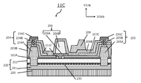
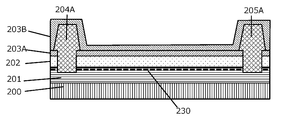
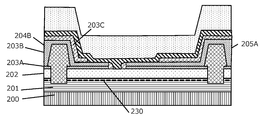
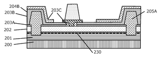
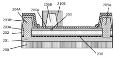
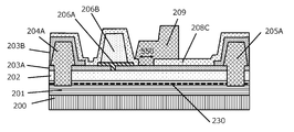
- FIG. 1A is a cross-sectional view showing the structure of the power amplification semiconductor device according to the first embodiment.
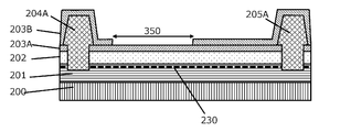
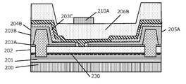
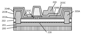
- FIG. 1B is a cross-sectional view showing the structure of the power amplification semiconductor device according to the second and fourth embodiments.
- FIG. 1C is a cross-sectional view showing the structure of the power amplification semiconductor device according to the second embodiment.
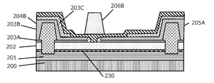
- FIG. 1D is a cross-sectional view showing the structure of the power amplification semiconductor device according to the third embodiment.
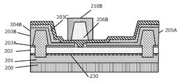
- FIG. 1E is a cross-sectional view showing the structure of the power amplification semiconductor device according to the fifth embodiment.
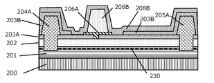
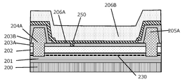
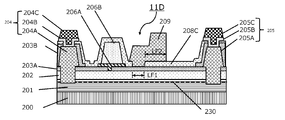
- FIG. 1F is a cross-sectional view showing the structure of the power amplification semiconductor device according to the sixth embodiment.
- FIG. 1A is a cross-sectional view showing the structure of the power amplification semiconductor device according to the first embodiment.
- FIG. 1B is a cross-sectional view showing the structure of the power amplification semiconductor device according to the second and fourth embodiments.
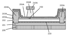
- FIG. 1G is a cross-sectional view showing the structure of the power amplification semiconductor device according to the seventh embodiment.
- FIG. 1H is a cross-sectional view showing the structure of the power amplification semiconductor device according to the eighth embodiment.
- FIG. 1I is a cross-sectional view showing the structure of the power amplification semiconductor device according to the eighth embodiment.
- FIG. 1J is a diagram illustrating a mechanism of the power amplification semiconductor device according to the second embodiment.
- FIG. 1K is a diagram illustrating a mechanism of the power amplification semiconductor device according to the second embodiment.
- FIG. 1L is a diagram illustrating the mechanism of the power amplification semiconductor device according to the second embodiment.
- FIG. 1M is a diagram illustrating a mechanism of the power amplification semiconductor device according to the second embodiment.
- FIG. 1N is a diagram illustrating the mechanism of the power amplification semiconductor device according to the second embodiment.
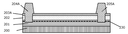
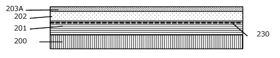
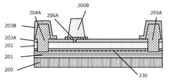
- FIG. 2A is a cross-sectional view showing the structure of the power amplification semiconductor device according to the first embodiment during manufacturing.
- FIG. 2B is a cross-sectional view showing the structure of the power amplification semiconductor device according to the first embodiment during manufacturing.
- FIG. 2C is a cross-sectional view showing the structure of the power amplification semiconductor device according to the first embodiment during manufacturing.
- FIG. 2D is a cross-sectional view showing the structure of the power amplification semiconductor device according to the first embodiment during manufacturing.
- FIG. 2E is a cross-sectional view showing the structure of the power amplification semiconductor device according to the first embodiment during manufacturing.
- FIG. 2A is a cross-sectional view showing the structure of the power amplification semiconductor device according to the first embodiment during manufacturing.
- FIG. 2B is a cross-sectional view showing the structure of the power amplification semiconductor device according to the first embodiment
- FIG. 2F is a cross-sectional view showing the structure of the power amplification semiconductor device according to the first embodiment during manufacturing.
- FIG. 2G is a cross-sectional view showing the structure of the power amplification semiconductor device according to the first embodiment during manufacturing.
- FIG. 2H is a cross-sectional view showing the structure of the power amplification semiconductor device according to the first embodiment during manufacturing.
- FIG. 2I is a cross-sectional view showing the structure of the power amplification semiconductor device according to the first embodiment during manufacturing.
- FIG. 2J is a cross-sectional view showing the structure of the power amplification semiconductor device according to the first embodiment during manufacturing.
- FIG. 2K is a cross-sectional view showing the structure of the power amplification semiconductor device according to the first embodiment during manufacturing.
- FIG. 2L is a cross-sectional view showing the structure of the power amplification semiconductor device according to the first embodiment during manufacturing.
- FIG. 2M is a cross-sectional view showing the structure of the power amplification semiconductor device according to the first embodiment during manufacturing.
- FIG. 2N is a cross-sectional view showing the structure of the power amplification semiconductor device according to the first embodiment during manufacturing.
- FIG. 2O is a cross-sectional view showing the structure of the power amplification semiconductor device according to the first embodiment during manufacturing.
- FIG. 2P is a cross-sectional view showing the structure of the power amplification semiconductor device according to the first embodiment during manufacturing.
- FIG. 2Q is a cross-sectional view showing the structure of the power amplification semiconductor device according to the first embodiment during manufacturing.
- FIG. 2R is a cross-sectional view showing the structure of the power amplification semiconductor device according to the first embodiment during manufacturing.
- FIG. 3A is a cross-sectional view showing the structure of the power amplification semiconductor device according to the second embodiment in the manufacturing process.
- FIG. 3B is a cross-sectional view showing the structure of the power amplification semiconductor device according to the second embodiment during manufacturing.
- FIG. 3C is a cross-sectional view showing the structure of the power amplification semiconductor device according to the second embodiment during manufacturing.
- FIG. 3D is a cross-sectional view showing the structure of the power amplification semiconductor device according to the second embodiment in the manufacturing process.
- FIG. 3E is a cross-sectional view showing the structure of the power amplification semiconductor device according to the second embodiment during manufacturing.
- FIG. 3A is a cross-sectional view showing the structure of the power amplification semiconductor device according to the second embodiment in the manufacturing process.
- FIG. 3B is a cross-sectional view showing the structure of the
- FIG. 3F is a cross-sectional view showing the structure of the power amplification semiconductor device according to the second embodiment during manufacturing.
- FIG. 3G is a cross-sectional view showing the structure of the power amplification semiconductor device according to the second embodiment in the manufacturing process.
- FIG. 3H is a cross-sectional view showing the structure of the power amplification semiconductor device according to the second embodiment during manufacturing.
- FIG. 3I is a cross-sectional view showing the structure of the power amplification semiconductor device according to the second embodiment during manufacturing.
- FIG. 3J is a cross-sectional view showing the structure of the power amplification semiconductor device according to the second embodiment during manufacturing.
- FIG. 3K is a cross-sectional view showing the structure of the power amplification semiconductor device according to the second embodiment in the manufacturing process.
- FIG. 3L is a cross-sectional view showing the structure of the power amplification semiconductor device according to the second embodiment during manufacturing.
- FIG. 3M is a cross-sectional view showing the structure of the power amplification semiconductor device according to the second embodiment during manufacturing.
- FIG. 3N is a cross-sectional view showing the structure of the power amplification semiconductor device according to the second embodiment during manufacturing.
- FIG. 3O is a cross-sectional view showing the structure of the power amplification semiconductor device according to the second embodiment in the manufacturing process.
- FIG. 3P is a cross-sectional view showing the structure of the power amplification semiconductor device according to the second embodiment in the manufacturing process.
- FIG. 3Q is a cross-sectional view showing the structure of the power amplification semiconductor device according to the second embodiment in the manufacturing process.
- FIG. 3R is a cross-sectional view showing the structure of the power amplification semiconductor device according to the second embodiment during manufacturing.
- FIG. 4A is a cross-sectional view showing the structure of the power amplification semiconductor device according to the fifth embodiment during manufacturing.
- FIG. 4B is a cross-sectional view showing the structure of the power amplification semiconductor device according to the fifth embodiment during manufacturing.
- FIG. 4C is a cross-sectional view showing the structure of the power amplification semiconductor device according to the fifth embodiment during manufacturing.
- FIG. 4D is a cross-sectional view showing the structure of the power amplification semiconductor device according to the fifth embodiment during manufacturing.
- FIG. 4E is a cross-sectional view showing the structure of the power amplification semiconductor device according to the fifth embodiment during manufacturing.
- FIG. 4A is a cross-sectional view showing the structure of the power amplification semiconductor device according to the fifth embodiment during manufacturing.
- FIG. 4B is a cross-sectional view showing the structure of the power amplification semiconductor device
- FIG. 4F is a cross-sectional view showing the structure of the power amplification semiconductor device according to the fifth embodiment during manufacturing.
- FIG. 4G is a cross-sectional view showing the structure of the power amplification semiconductor device according to the fifth embodiment during manufacturing.
- FIG. 4H is a cross-sectional view showing the structure of the power amplification semiconductor device according to the fifth embodiment during manufacturing.
- FIG. 4I is a cross-sectional view showing the structure of the power amplification semiconductor device according to the fifth embodiment during manufacturing.
- FIG. 4J is a cross-sectional view showing the structure of the power amplification semiconductor device according to the fifth embodiment during manufacturing.
- FIG. 4K is a cross-sectional view showing the structure of the power amplification semiconductor device according to the fifth embodiment during manufacturing.
- FIG. 4L is a cross-sectional view showing the structure of the power amplification semiconductor device according to the fifth embodiment during manufacturing.
- FIG. 4M is a cross-sectional view showing the structure of the power amplification semiconductor device according to the fifth embodiment during manufacturing.
- FIG. 4N is a cross-sectional view showing the structure of the power amplification semiconductor device according to the fifth embodiment during manufacturing.
- FIG. 4O is a cross-sectional view showing the structure of the power amplification semiconductor device according to the fifth embodiment during manufacturing.
- FIG. 4P is a cross-sectional view showing the structure of the power amplification semiconductor device according to the fifth embodiment during manufacturing.
- FIG. 4Q is a cross-sectional view showing the structure of the power amplification semiconductor device according to the fifth embodiment during manufacturing.
- FIG. 4M is a cross-sectional view showing the structure of the power amplification semiconductor device according to the fifth embodiment during manufacturing.
- FIG. 4N is a cross-sectional view showing the structure of the power amplification semiconductor device
- FIG. 4R is a cross-sectional view showing the structure of the power amplification semiconductor device according to the fifth embodiment during manufacturing.
- FIG. 4S is a cross-sectional view showing the structure of the power amplification semiconductor device according to the fifth embodiment during manufacturing.
- FIG. 4T is a cross-sectional view showing the structure of the power amplification semiconductor device according to the fifth embodiment during manufacturing.
- FIG. 4U is a cross-sectional view showing the structure of the power amplification semiconductor device according to the fifth embodiment during manufacturing.
- FIG. 5A is a cross-sectional view showing the structure of the power amplification semiconductor device according to the sixth embodiment during manufacturing.
- FIG. 5B is a cross-sectional view showing the structure of the power amplification semiconductor device according to the sixth embodiment during manufacturing.
- FIG. 5C is a cross-sectional view showing the structure of the power amplification semiconductor device according to the sixth embodiment during manufacturing.
- FIG. 5D is a cross-sectional view showing the structure of the power amplification semiconductor device according to the sixth embodiment during manufacturing.
- FIG. 5E is a cross-sectional view showing the structure of the power amplification semiconductor device according to the sixth embodiment during manufacturing.
- FIG. 5F is a cross-sectional view showing the structure of the power amplification semiconductor device according to the sixth embodiment during manufacturing.
- FIG. 5G is a cross-sectional view showing the structure of the power amplification semiconductor device according to the sixth embodiment during manufacturing.
- FIG. 5H is a cross-sectional view showing the structure of the power amplification semiconductor device according to the sixth embodiment during manufacturing.
- FIG. 5I is a cross-sectional view showing the structure of the power amplification semiconductor device according to the sixth embodiment during manufacturing.
- FIG. 5J is a cross-sectional view showing the structure of the power amplification semiconductor device according to the sixth embodiment during manufacturing.
- FIG. 5K is a cross-sectional view showing the structure of the power amplification semiconductor device according to the sixth embodiment during manufacturing.
- FIG. 5L is a cross-sectional view showing the structure of the power amplification semiconductor device according to the sixth embodiment during manufacturing.
- FIG. 5M is a cross-sectional view showing the structure of the power amplification semiconductor device according to the sixth embodiment during manufacturing.
- FIG. 5N is a cross-sectional view showing the structure of the power amplification semiconductor device according to the sixth embodiment during manufacturing.
- FIG. 5O is a cross-sectional view showing the structure of the power amplification semiconductor device according to the sixth embodiment during manufacturing.
- FIG. 5P is a cross-sectional view showing the structure of the power amplification semiconductor device according to the sixth embodiment during manufacturing.
- FIG. 5Q is a cross-sectional view showing the structure of the power amplification semiconductor device according to the sixth embodiment during manufacturing.
- FIG. 5R is a cross-sectional view showing the structure of the power amplification semiconductor device according to the sixth embodiment during manufacturing.
- FIG. 5S is a cross-sectional view showing the structure of the power amplification semiconductor device according to the sixth embodiment during manufacturing.
- FIG. 5T is a cross-sectional view showing the structure of the power amplification semiconductor device according to the sixth embodiment during manufacturing.
- FIG. 5U is a cross-sectional view showing the structure of the power amplification semiconductor device according to the sixth embodiment during manufacturing.
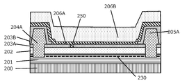
- the power amplification semiconductor device 10 of FIG. 1A is a cross-sectional view showing the structure of the power amplification semiconductor device according to the first embodiment.
- the semiconductor device for power amplification includes a substrate 200, a semiconductor laminate 220, a source electrode 204, a drain electrode 205, a gate electrode 206, a source field plate 209, an insulating film 203A, and the like.
- the insulating film 203B and the insulating film 208 are provided.
- the substrate 200 is configured by stacking a buffer layer on, for example, a Si substrate.
- a semiconductor laminate 220 which will be described later, is epitaxially grown on the upper part of the substrate 200.
- a SiC substrate, a sapphire substrate, or a diamond substrate may be used.
- the original Si substrate may be peeled off and replaced with another substrate.
- the buffer layer is, for example, a nitride semiconductor having a plurality of laminated structures of AlN and AlGaN.
- the buffer layer may also be composed of a single layer or a plurality of layers of group III nitride semiconductors such as GaN, AlGaN, AlN, InGaN, and AlInGaN.
- the semiconductor laminate 220 is composed of a first nitride semiconductor layer 201 formed on the substrate 200 and a second nitride semiconductor layer 202 formed on the first nitride semiconductor layer 201.
- the first nitride semiconductor layer 201 is a GaN channel layer made of gallium nitride (GaN).
- the first nitride semiconductor layer 201 can be formed of, for example, undoped (i-type) GaN having a thickness of 200 nm. Undoping (i-type) means that impurities are not intentionally doped during epitaxial growth.
- the first nitride semiconductor layer 201 is not limited to GaN, and may be composed of a group III nitride semiconductor such as InGaN, AlGaN, or AlInGaN, or may contain n-type impurities.
- the second nitride semiconductor layer 202 is an Al x Ga 1-x N barrier layer made of aluminum gallium nitride (Al x Ga 1-x N (0 ⁇ x ⁇ 1)).
- the second nitride semiconductor layer 202 is composed of, for example, an undoped (i-type) Al x Ga 1-x N having a thickness of 20 nm and an Al composition ratio of 25%.
- the second nitride semiconductor layer 202 is not limited to Al x Ga 1-x N, but may be composed of a group III nitride semiconductor such as AlN, InGaN, or AlInGaN, and contains n-type impurities. May be.
- the band gap of the second nitride semiconductor layer 202 is larger than the band gap of the first nitride semiconductor layer 201.
- the second nitride semiconductor layer 202 made of undoped (i-type) Al x Ga 1-x N and the first nitride semiconductor layer 201 made of undoped (i-type) GaN have a heterostructure. That is, the interface between the second nitride semiconductor layer 202 and the first nitride semiconductor layer 201 is heterojunctioned, and the interface between the second nitride semiconductor layer 202 and the first nitride semiconductor layer 201 has a heterobarrier. It is formed.
- 2DEG is generated on the first nitride semiconductor layer 201 side of the hetero interface between the second nitride semiconductor layer 202 and the first nitride semiconductor layer 201, and the 2DEG surface 230 is formed.
- the source electrode 204 is formed on the semiconductor laminate 220 and includes an ohmic portion 204A, a barrier metal portion 204B, and a wiring 204C.
- the drain electrode 205 is formed on the semiconductor laminate 220 and includes an ohmic portion 205A, a barrier metal portion 205B, and a wiring 205C.
- the gate electrode 206 is formed on the semiconductor laminate 220 between the source electrode 204 and the drain electrode 205, and is composed of a lower layer 206A and an upper layer 206B.
- the lower layer 206A above the first insulating layer 203A is generally called a gate field plate.
- the source field plate 209 is formed on the semiconductor laminate 220 between the gate electrode 206 and the drain electrode 205 so as not to cover the gate electrode 206.
- the source field plate 209 is provided with the same potential as the source electrode 204.
- the lower surface of the source field plate 209 facing the second nitride semiconductor layer 202 will be referred to as the lowermost surface of the source field plate.
- FIGS. 2A to 2R are cross-sectional views showing the structure of the power amplification semiconductor device 10 in the process of manufacturing, respectively.
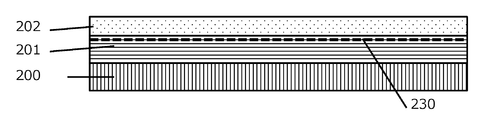
- the first nitride semiconductor layer 201 is epitaxially grown on the substrate 200, and then the second nitride semiconductor layer 202 is epitaxially grown on the substrate 200 to obtain the first nitride semiconductor.
- the layer 201 and the second nitride semiconductor layer 202 are laminated.
- the ohmic electrode opening 240A for forming the source electrode 204 that is ohmic-bonded to the semiconductor laminate 220 and the drain electrode 205 that is ohmic-bonded to the semiconductor laminate 220 are formed by the dry etching opening.
- the ohmic electrode opening 240B for forming is formed.
- This dry etching opening is performed by etching the insulating film 203A, etching the second nitride semiconductor layer 202, and further etching the first nitride semiconductor layer 201 until the 2DEG surface 230 appears.
- the ohmic portion 204A is formed in the ohmic electrode opening 240A, and the ohmic portion 205A is formed in the ohmic electrode opening 240B.
- the ohmic part 204A and the ohmic part 205A are both made of the same material, and are, for example, materials containing Ti and Al.
- the ohmic portion 204A and the ohmic portion 205A are formed by continuously depositing Ti and Al metals on the entire upper surface of the insulating film 203A including the region of the ohmic electrode opening 240A and the ohmic electrode opening 240B by a sputtering method. It is formed by forming a resist mask on the ohmic portion 204A and the ohmic portion 205A by photolithography and then removing the portions other than the ohmic portion 204A and the ohmic portion 205A by dry etching.
- the ohmic portion 204A and the ohmic portion 205A may be formed by depositing Ti and Al metals on the ohmic electrode opening 240A and the ohmic electrode opening 240B, respectively, by a vapor deposition / lift-off method.
- the semiconductor laminate 220 and the metal of Ti and Al are alloyed with each other at a high temperature exceeding 500 ° C. to perform ohmic contact between the metal and the semiconductor. It utilizes the property that when N of Ti and GaN reacts, it is easily formed into an N type.
- an insulating film is deposited 203B made of Si 3 N 4.
- the ohmic portion 204A and the ohmic portion 205A are covered with a photoresist mask, the insulating film 203B is removed by etching, and the insulating film 203A is exposed.
- a gate opening 250 for Schottky joining the lower layer 206A and the second nitride semiconductor layer 202 is formed in the insulating film 203A.
- the gate opening 250 is formed by opening a pattern by resist-coated photolithography and then etching and removing the insulating film 203A until the upper surface of the second nitride semiconductor layer 202 is exposed.
- This etching is usually is realized by a dry etching the Si 3 N 4 with a gas containing CF 4, it may be realized by wet etching using HF. Alternatively, it may be realized by a method of synthesizing the dry etching and the wet etching.
- the lower layer 206A and the upper layer 206B are continuously deposited on the entire upper surface of the insulating film 203A including the insulating film 203B and the gate opening 250 by a sputtering method.
- the sputtering method is a method of depositing a desired metal material on the surface of a semiconductor substrate facing the target by colliding accelerated ions with the target surface of the metal species to be deposited on the semiconductor substrate.
- the lower layer 206A needs to be Schottky-bonded to the second nitride semiconductor layer 202. Therefore, the lower layer 206A is, for example, a metal containing TiN.
- the upper layer 206B is for lowering the overall resistance value of the gate electrode 206. Therefore, the upper layer 206B is, for example, a metal containing Al.
- TiN in the material example of the lower layer 206A is a highly refractory metal. Therefore, the lower layer 206A also functions as a barrier metal at high temperature between the upper layer 206B and the second nitride semiconductor layer 202.
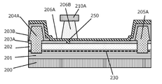
- a resist mask 210A having a pattern is formed in the formed region of the gate electrode 206 by photolithography patterning so that only the desired region of the upper layer 206B remains.
- the upper layer 206B in the region where the resist mask 210A is not formed is removed by vertical dry etching, and the dry etching is stopped when the lower layer 206A is exposed.
- the resist mask 210A is removed with, for example, an organic solvent.
- a resist mask 210B is formed by photolithography patterning so as to cover the upper layer 206B and the desired region of the lower layer 206A.
- the lower layer 206A is removed by dry etching.
- the end point of this etching is where the insulating film 203A is exposed.
- the resist mask 210B is removed with, for example, an organic solvent.
- the resist mask 210B may be formed closer to the drain electrode 205 side than the gate opening 250.
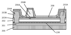
- the insulating film 208 is deposited on the entire upper surface of the insulating film 203A including the insulating film 203B, the lower layer 206A, and the upper layer 206B.
- the source field plate 209 is formed on the flat surface of the insulating film 208 of the gate electrode 206 composed of the lower layer 206A and the upper layer 206B.
- the source field plate 209 for example, Ti and Al are continuously deposited on the entire upper surface of the insulating film 208 by a sputtering method, and then a resist mask is formed at a desired position by photolithography, and the portion not covered with the resist mask. Is formed by removing with dry etching.
- the insulating film 203B and the insulating film 208 on the ohmic portion 204A and the insulating film 203B and the insulating film 208 on the ohmic portion 205A are etched and opened, and the contact portion 270A and the contact portion 270B are opened. And form.
- a barrier metal portion 204B and a barrier metal portion 205B made of a refractory metal such as W and TiN are placed on the contact portion 270A and the contact portion 270B, respectively.
- a wiring 204C and a wiring 205C made of a metal made of, for example, Au, Al, or Cu are formed on the barrier metal portion 204B and the barrier metal portion 205B by a plating method, respectively. ..
- the power amplification semiconductor device 10 shown in FIG. 1A is completed.
- the gate electrode 206 is described as being composed of the lower layer 206A and the upper layer 206B.
- the gate electrode 206 does not necessarily have to be limited to a structural example including the lower layer 206A and the upper layer 206B.
- the gate electrode 206 has a structure having no layer structure (hereinafter, “integrated structure”). It may also be referred to as).
- the material of the gate electrode 206 having an integrated structure may be any metal material capable of Schottky-bonding the gate electrode 206 and the second nitride semiconductor layer 202. Specifically, for example, Ni, TiN, Pt. , Pd, Cu, Ta, TaN, W, WSi, Al and the like.
- the gate electrode 206 when the gate electrode 206 is composed of the lower layer 206A and the upper layer 206B, the lower layer 206A and the upper layer 206B can be made of different materials.
- the above is a method for manufacturing a power amplification semiconductor device 10 in which a gate electrode 206 and a source field plate 209 are manufactured by a sputtering / dry etching method.
- the power amplification semiconductor device 10 includes a gate electrode 206 and a source field plate. It is also possible to manufacture 209 by a vapor deposition / lift-off method.
- a photoresist mask is formed so that the electrode forming region is opened, and a metal composed of Ni and Au is continuously vapor-deposited from the upper layer thereof.
- the metal to be deposited on the semiconductor substrate is deposited on the semiconductor substrate by heating it in a vacuum to a temperature higher than the melting point by resistance heating or an electron beam and melting it.
- the photoresist mask is removed with an organic solvent.
- the electrodes on the photoresist mask are removed at the same time as the photoresist mask.
- the gate electrode 206 having the lower layer 206A as Ni and the upper layer 206B as Au is left in the gate electrode 206 portion of the opening of the photoresist mask.
- the vapor deposition / lift-off method has the advantages of being simple in terms of manufacturing method and causing less damage to the semiconductor substrate, but the sputtering / dry etching method is superior in terms of dimensional accuracy.
- Cds which has a strong correlation with the low power consumption characteristics of a semiconductor device for power amplification for high frequencies, is the capacitance generated between the source field plate and the electrodes formed on the facing 2DEG surfaces 230. This capacitance is inversely proportional to the electrode spacing and proportional to the electrode area.
- the present invention is characterized in that the height position of the lowermost surface of the source field plate is higher than the position of the lower surface of the gate field plate, so that the distance is wider than the electrode spacing in Patent Document 1. Therefore, the capacitance generated between the electrodes in the power amplification semiconductor device 10 is smaller than the capacitance generated between the electrodes in Patent Document 1.
- the power amplification semiconductor device 10 having the above configuration, it is possible to achieve both relaxation of the electric field between the gate electrode and the drain electrode by the source field plate and suppression of Cds.
- the height HG of the uppermost surface of the gate electrode 206 can be made higher than the height HS of the upper end position of the side surface closest to the gate side, so that the gate resistance Rg is reduced. can do. This is because the gate resistance Rg is generally inversely proportional to the cross-sectional area of the gate electrode.
- this structure can easily reduce the parasitic capacitance (hereinafter referred to as Cgs) generated between the side surface of the gate electrode 206 and the side surface of the source field plate 209 which is in close contact with the gate side.
- Cgs parasitic capacitance
- the upper surface portion of the gate electrode 206 in FIG. 1A is protected with an insulating film made of Si 3 N 4 and then a source field plate.
- a structure in which 209 covers the gate electrode 206 is common.
- the height of the uppermost surface of the gate electrode 206 cannot be sufficiently increased due to the problem of manufacturing stability of the step coverage of the covering portion covering the upper surface of the gate electrode 206. This is because if the height is increased, a problem occurs in the covering property of the source field plate due to cracks, and as a result, the resistance component of the source field plate varies.
- the structure of the present invention having a shape in which the source field plate 209 does not cover the gate electrode 206 can reduce the gate resistance Rg as compared with a general semiconductor device for power amplification.
- the gain characteristics in the high frequency band can be further improved as compared with the general power amplification semiconductor device.
- FIG. 1A there is a slight gap between the drain end of the gate field plate made of the lower layer 206A and the gate side end of the source field plate 209, but if this gap is too wide, the electric field of the source field plate The mitigation effect becomes weaker, the increase in parasitic capacitance (hereinafter referred to as Cgd) between the gate and drain cannot be ignored, and the gain decreases.
- Cgd parasitic capacitance
- the electric field dispersion can be corrected by adjusting the length of the source field plate 209 in the X direction shown in FIG. 1A, so that no problem occurs.
- the X direction is a direction from the source electrode to the drain electrode in a cross-sectional view.
- the power amplification semiconductor device 11 of FIG. 1B is a cross-sectional view showing the structure of the power amplification semiconductor device according to the second embodiment.
- the power amplification semiconductor device 11 includes a substrate 200, a semiconductor laminate 220, a source electrode 204, a drain electrode 205, a gate electrode 206, a source field plate 209, and an insulating film 203A. , The insulating film 203B and the insulating film 208 are provided.
- the difference from the power amplification semiconductor device 10 of FIG. 1A is that the source field plate 209 has a stepped shape.
- the lower side is referred to as a first source field plate and the upper side is referred to as a second source field plate.
- 3A to 3R are cross-sectional views showing the structure of the power amplification semiconductor device 11 in the process of manufacturing, respectively.
- the insulating film 203B includes the gate opening 250 and forms a wider opening 350. At this time, the opening close to the ohmic portion 205A becomes the boundary between the lower and upper stages of the source field plate 209.
- a gate opening 250 is formed to expose the second nitride semiconductor layer 202.
- the gate electrodes 206 (206A, 206B) are formed by the same manufacturing method as the steps described in FIGS. 2H to 2N of the first embodiment.
- the insulating film 208B is deposited on the entire surface.
- the source field plate 209 is deposited.
- the source electrode 204 and the drain electrode 205 are formed by the same manufacturing method as the steps described in FIGS. 2Q to 2R of the first embodiment.
- the power amplification semiconductor device 11 shown in FIG. 1B is completed.
- FIG. 1N shows a comparison between the electric field distribution in the X direction and the parasitic capacitance Cds generated on the source field plate 209 and the 2DEG surface 230 of the semiconductor laminate 220.
- FIG. 1N (a) shows no source field plate 209, FIG. 1N (b) shows source field plate 209 arranged, FIG. 1N (c) shows more source field plates than FIG. 1N (b).
- FIG. 1N (d) in FIG. 1N is a case where the source field plate 209 is stepped.
- the electric field peak at the drain side end position on the lower surface of the source field plate is the drain side end position on the lower surface of the second source field plate. It is dispersed up to X3). At this time, since the distance between the 2DEG surface 230 and the lower surface of the second source field plate becomes long, the parasitic capacitance Cds is smaller than that in FIG. 1N (c).
- the present embodiment has a structure that achieves both relaxation of the electric field and reduction of the parasitic capacitance Cds.
- the desirable dimensions of the source field plate 209 will be described with reference to FIG. 1B. That is, it is a condition regarding the X direction and the Y direction deduced from the effect mechanism of making the source field plate stepped.
- the height of the uppermost surface of the gate electrode 206 is HG
- the height of the upper end position of the side surface closest to the gate side of the first source field plate is HS1
- the height of the upper end position is closest to the gate side of the second source field plate.
- the height of the upper end position of the side surface is HS2.
- the uppermost surface gate side end position of the drain electrode 205 is viewed from the uppermost surface drain side end position of the gate electrode 206, it is blocked by the source field plate 209. That is, when shielded by the source field plate 209, it is effective in reducing the parasitic capacitance Cgd between the gate and drain electrodes. That is, HS2> HG is desirable.
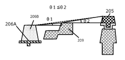
- FIG. 1J and Fig. 1K show the angle at which the uppermost surface gate side end position of the drain electrode 205 is viewed from the uppermost surface drain side end position of the gate electrode 206.
- FIG. 1J shows the case where the second source field plate is relatively high
- FIG. 1K shows the case where the second source field plate is relatively low.
- the elevation angle ⁇ 1 when the uppermost surface gate side end position of the second source field plate is viewed from the uppermost surface drain side end position of the gate electrode 206 is from the uppermost surface gate side end position of the second source field plate. It is larger than the elevation angle ⁇ 2 when the position of the uppermost gate side end of the drain electrode 205 is viewed. That is, when expressed using the elevation angle, ⁇ 1> ⁇ 2. By making this relationship, the shielding effect can be strengthened.
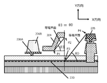
- FIG. 1L shows a case where the difference between the height of the first source field plate and the height of the second source field plate is large
- FIG. 1M shows the case where the difference between the height of the first source field plate and the height of the second source field plate is small.
- the elevation angle ⁇ 3 when the lower surface drain side end position of the second source field plate is viewed from the lower surface drain side end position of the first source field plate is the second source field plate.
- the portion of the 2DEG surface 230 that is not depleted by the source field plate 209 is the portion on the drain electrode 205 side from the point P3 in FIG. 1L.
- Point P3 is the intersection of the line drawn from the drain electrode side end of the source field plate 209 toward the 2DEG surface 230 and the 2DEG surface 230.
- an equal electric field is also formed on the line connecting the points P1 and P2 of the source field plate 209 parallel to it.
- Point P1 indicates the drain side end of the lower part of the source field plate 209
- point P2 indicates the drain side end of the upper part of the source field plate 209.
- the point P1 at which the electric field peak is desired to be lowered has the same electric field as the point P2, which means that the electric field relaxation at the point P1 is insufficient.
- the line including the point P2 that is parallel to the reference line connecting the points P3 and P4 is a line connecting the point P2 and the point P5 in the figure, and has an equal electric field on this line. ..
- the point P1 for which the electric field is to be relaxed appears to be deeper (farther) than the line connecting the points P2 and P5 when viewed from the reference line, that is, the electric field is lower than the point P2.
- the point P2 is in a state where the electric field is relaxed at the point P1. This is a preferable shape condition from the viewpoint of electric field relaxation for the source field plate 209. Expressing this condition in terms of elevation angle, ⁇ 3 ⁇ 0.
- the source field plate 209 may have a structure in which the first source field plate (209A) and the second source field plate (209B) are separated.
- the power amplification semiconductor device 11B of FIG. 1D is a cross-sectional view showing the structure of the power amplification semiconductor device according to the third embodiment.
- the power amplification semiconductor device 11B is a source composed of a substrate 200, a semiconductor laminate 220, a source electrode 204, a drain electrode 205, a gate electrode 206, a lower layer metal 209C, and an upper layer metal 209D.
- a field plate 209, an insulating film 203A, an insulating film 203B, and an insulating film 208B are provided.
- the first source field plate and the second source field plate of the source field plate 209 have the same metal film thickness due to the manufacturing method. , It is a structure that can be easily formed by depositing metal only on the second source field plate by adding another step.
- a metal having three layers of TiN, AL, and TiN deposited as the lower metal 209C, and a low resistance metal AL as the upper metal 209D are used.
- the AL of the lower metal 209C has a film thickness of 300 nm or more.
- FIG. 1D is characterized by a structure having a metal layer having a lower electrical resistivity than the second source field plate only on the second source field plate.
- the parasitic capacitance Cgs between the side surface of the upper layer 206B of the gate metal and the source field plate 209 is reduced.
- a low resistance source field plate 209 can be obtained by thickening the metal of the second source field plate.
- the lower metal 209C is deposited on the step formed by the insulating film 203A and the insulating film 203B.
- the metal to be deposited can be made of high quality, which is denser and has lower electrical resistance when it is deposited on the flat part of the step than when it is deposited on the side wall of the step.
- the upper layer metal 209D which is a thick film low resistance metal, is additionally deposited only on the upper second source field plate.
- the lower metal 209C and the upper metal 209D do not have to be dissimilar metals as described above, and may be the same kind of metal.
- a metal composed of AL may be deposited on the lower metal 209C, and then AL may be deposited again as the upper metal 209D.
- the power amplification semiconductor device 11 of FIG. 1B is a cross-sectional view showing the structure of the power amplification semiconductor device according to the fourth embodiment.
- the power amplification semiconductor device 11 includes a substrate 200, a semiconductor laminate 220, a source electrode 204, a drain electrode 205, a gate electrode 206, a source field plate 209, and an insulating film 203A. , The insulating film 203B and the insulating film 208B are provided.
- Table 1 shows the combinations of the insulating films 203B and 208B of the power amplification semiconductor device 11.
- the insulating films 203B and 208B described with respect to the structure of the semiconductor device for power amplification according to the first to third embodiments are the case of the combination A of the insulating films in Table 1, and the lower insulating films 203B are from Si 3 N 4.
- the upper insulating film 208B is made of Si 3 N 4 .
- SiO 2 is an insulating film, it does not necessarily have to be Si 3 N 4 , and SiO 2 having a lower dielectric constant is also possible.
- the relative permittivity of Si 3 N 4 is about 7
- the relative permittivity of SiO 2 is about 4
- SiO 2 is an insulating film having a lower dielectric constant.
- a low dielectric constant insulating film there is also SiON in which O and N are mixed crystals, which is also a candidate as a low dielectric constant film.
- SiO 2 is described as an example.
- the manufacturing method is the same as the method of the second embodiment described with reference to FIGS. 3A to 3R, and the description thereof will be omitted.
- Deposition temperature conditions, the etching time condition is generated with the film quality change, Common deposition for Si 3 N 4, SiO 2, may be used etching conditions.
- This structure (combination of FIG. 1B and Table 1B) has the effect of further reducing the parasitic capacitance Cds between the second source field plate and the 2DEG surface 230.
- the power amplification semiconductor device 11C of FIG. 1E is a cross-sectional view showing the structure of the power amplification semiconductor device according to the fifth embodiment.
- the power amplification semiconductor device 11C includes a substrate 200, a semiconductor laminate 220, a source electrode 204, a drain electrode 205, a gate electrode 206, a source field plate 209, and an insulating film 203A. , The insulating film 203B, the insulating film 203C, and the insulating film 208B.
- This manufacturing method is called the sidewall process. It is a manufacturing method often used when forming a fine gate dimension of 0.25 ⁇ m or less without using an electron beam (EB) drawing method, which has a poor manufacturing throughput and a high cost.
- EB electron beam
- 4A to 4U are cross-sectional views showing the structure of the power amplification semiconductor device 11C in the process of manufacturing, respectively.
- FIG. 4E is the same as the manufacturing method from FIGS. 2A to 2E described above, and the description thereof will be omitted.
- the region where the gate electrode 206 is formed is patterned with a photoresist, and the insulating film 203B and the insulating film 203A are continuously etched to form the opening 450. At that time, the process is performed until the outermost surface of the semiconductor laminate 220 is exposed.
- the insulating film 203C is deposited on the entire surface.
- a wall of the insulating film 203C is formed on the side surface of the opening 450.
- the resist mask 400 is formed so that the region forming the gate electrode 206 is opened.
- the insulating film 203C is etched using the resist mask 400 until the surface of the insulating film 203B is exposed. At that time, as shown in FIG. 4I, only the wall of 203C on the side surface (side) of the openings 450, 203B, 203A remains. The dimension between the sidewalls is shorter than the original dimension of the opening 450 by the wall.
- the manufacturing method that realizes miniaturized dimensions is the sidewall process.
- the gate electrode 206 is formed by the same manufacturing method as in FIGS. 2H to 2N described above.
- the insulating film 208B is deposited on the entire surface.
- the source field plate 209 is deposited by the method already described as shown in the figure.
- the source electrode 204 and the drain electrode 205 are formed by the same manufacturing method as the steps described in FIGS. 2Q to 2R of the first embodiment, and the power amplification semiconductor device 11C is completed. do.
- Table 2 shows an example of the combination of the insulating film 208B and the insulating film 203C.
- the embodiment 2 has already been performed. It provides the above-mentioned combination A in Table 1 of FIG. 1B and, as a result, a second manufacturing method that remains unchanged and forms the same structure.
- the gate electrode is used due to the manufacturing method. Since the side surface (sidewall portion) of the 206 is made of the same material as the insulating film 203C, SiO 2 is formed on the side surface of the gate electrode 206.
- the power amplification semiconductor device 11D of FIG. 1F is a cross-sectional view showing the structure of the power amplification semiconductor device according to the sixth embodiment.
- the power amplification semiconductor device 11D includes a substrate 200, a semiconductor laminate 220, a source electrode 204, a drain electrode 205, a gate electrode 206, a source field plate 209, and an insulating film 203A.
- the insulating film 203B and the insulating film 208C are provided.
- the insulating film 203A corresponds to the first insulating layer
- the insulating film 208C corresponds to the second insulating layer.
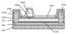
- 5A to 5U are cross-sectional views showing the structure of the power amplification semiconductor device 11D in the process of manufacturing, respectively.
- the manufacturing method is the same as that of FIGS. 2A to 2N described above, and the description thereof will be omitted.
- FIG. 5O shows a state in which the insulating film 208C made of SiO 2 is deposited on the entire surface after the gate electrode 206 is formed.
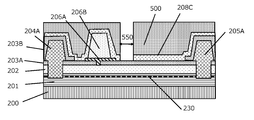
- FIG. 5P is a diagram in which the resist mask 500 for photoresist is patterned so that the opening 550 of the first source field plate is opened.
- FIG. 5Q shows a state in which the insulating film 208C is etched using the resist mask 500 for photoresist as a mask.
- the insulating film 208C contains SiO 2 , if it is etched with buffered hydrofluoric acid, the insulating film 203A under the insulating film 203A is Si 3 N 4 having a slow etching rate with respect to hydrofluoric acid. Etching processing can be selectively performed with good controllability.
- FIG. 5R shows a state in which the insulating film 208C is etched to remove the photoresist.
- the source field plate 209 is formed by the same method as before, it becomes as shown in FIG. 5S.
- the gate side of the source field plate 209 is covered with the insulating film 208C because the mask for patterning of the source field plate 209 is larger than the contact window of FIG. 5R. ..
- the power amplification semiconductor device 11D is completed as shown in FIG. 5U.
- the insulating film 208C has an opening 550 below the first source field plate, and the first source field plate has a structure in which the insulating film 203A comes into contact with the insulating film 203A via the opening 550. At this time, the lowermost position of the first source field plate is at the same height as the lowermost position of the lower layer 206A in contact with the insulating film 203A. Therefore, the electric field relaxation effect at the drain end position of the lower layer 206A becomes stronger. In addition, the Cgd reduction effect of the source field plate 209 is large, and high gain can be achieved by low Cgd.
- the parasitic capacitance Cds tends to increase because the lowermost position is close to the 2DEG surface 230. Therefore, as described in the second embodiment, in that case, the length LF1 of the lowermost surface of the source field plate 209 may be shortened, and the weakening electric field relaxation effect is obtained by the second source field plate in the upper stepped stage.
- the length LF2 may be lengthened and corrected.
- the insulating film 208C is a film having a low dielectric constant, so that the parasitic capacitance Cds with the semiconductor surface increases slowly, and the efficiency characteristics are not sacrificed.
- the structure of the power amplification semiconductor device 11D improves the trade-off between Cgd and Cds, which has been conventionally generated, and makes it possible to provide a power amplification semiconductor device having an excellent characteristic balance.
- the power amplification semiconductor device 11E of FIG. 1G is a cross-sectional view showing the structure of the power amplification semiconductor device according to the seventh embodiment.
- the power amplification semiconductor device 11E includes a substrate 200, a semiconductor laminate 220, a source electrode 204, a drain electrode 205, a gate electrode 206, a source field plate 209, and an insulating film 203A.
- the insulating film 203B, the insulating film 208B, and the protective film 210 are provided.
- the protective film 210 is an insulating film that protects the source field plate 209.
- the semiconductor device 11E for power amplification is formed by depositing , for example, an insulating film 210 made of SiO 2 having a low dielectric constant. can do.
- the surface parallel to the Y direction on the upper side of the stepped source field plate 209 faces the surface parallel to the Y direction of the drain electrode 205, and when the drain electrodes are close to each other, the parasitic capacitance Cds between the electrodes is ignored. become unable.
- the protective film 210 of the source field plate 209 is generally made of Si 3 N 4 , but since the parasitic capacitance Cds is proportional to the relative permittivity, the lower the dielectric constant of the protective film, the more desirable. Therefore, the seventh embodiment is characterized by a structure in which the protective film 210 is replaced with a SiO 2 having a low dielectric constant from the usual Si 3 N 4.
- GaN FETs In the future, as applications of GaN FETs, not only power amplifiers for base stations with a frequency of 6 GHz or less, which is currently the mainstream, but also applications in the millimeter wave band of the high frequency band, or applications of lower voltage for mobile terminals will be applied. If so, the gate-drain distance is shortened and the drain electrode is closer to the source field plate 209.
- the insulating film structure does not increase the parasitic capacitance Cds as in the seventh embodiment, high efficiency characteristics can be obtained even with the shortened gate-drain distance, and millimeter wave application and low voltage application for mobile terminals can be obtained. It is effective for.
- the power amplification semiconductor device 10A of FIG. 1H is a cross-sectional view showing the structure of the power amplification semiconductor device according to the eighth embodiment.
- the power amplification semiconductor device 10A includes a substrate 200, a semiconductor laminate 220, a source electrode 204, a drain electrode 205, a gate electrode 206, a source field plate 209, and an insulating film 203A. , The insulating film 203B and the insulating film 208 are provided.
- the length of the lower layer 206A in the X direction is on the drain side. This is the case when it is asymmetrically lengthened.
- the resist mask 210B which is the patterning mask of the lower layer 206A of FIG. 2L, is adjusted so as to be longer on the drain side, it is asymmetrically lengthened on the drain side. Can be done.
- the gate electrode 206 has a protrusion made of the lower layer 206A on the drain side.
- the protrusion will be located below the bottom surface of the source field plate 209. Due to this shape, the drain side end of the lower layer 206A where the electric field is strongest is completely protected by the source field plate 209, so that the electric field relaxation is effective.
- the amount of the protrusion sunk into the lower part of the source field plate 209 is the length LE from the gate end position of the source field plate 209 to the drain end of the lower layer 206A as shown in FIG. 1I.
- This length LE must not exceed the length LF1 of the bottom surface of the source field plate 209. If it exceeds the limit, the source field plate will be effectively shielded from the viewpoint of the semiconductor laminate 220, and the effect will be lost.
- the amount LE of the protrusion is less than half the length LF1 of the lowermost surface of the source field plate 209.
- the power amplification semiconductor device 11 of the second embodiment shown in FIG. 1B may be provided with the protrusion of the lower layer 206A, and the same effect may be obtained. Is obtained.
- the power amplification semiconductor device has been described above based on the first to eighth embodiments, but the present disclosure is not limited to these embodiments. As long as it does not deviate from the gist of the present disclosure, one or a plurality of embodiments of the present disclosure may be obtained by subjecting these embodiments to various modifications which a person skilled in the art can think of, or by combining components in different embodiments. It may be included within the scope of the embodiment.
- This disclosure can be widely used for power amplification semiconductor devices.
Landscapes
- Junction Field-Effect Transistors (AREA)
- Electrodes Of Semiconductors (AREA)
Priority Applications (4)
| Application Number | Priority Date | Filing Date | Title |
|---|---|---|---|
| US17/924,642 US12166103B2 (en) | 2020-05-13 | 2021-05-12 | Semiconductor device for power amplification |
| EP21803656.4A EP4135010B1 (en) | 2020-05-13 | 2021-05-12 | Semiconductor device for power amplification |
| JP2022522175A JP7307856B2 (ja) | 2020-05-13 | 2021-05-12 | 電力増幅用半導体装置 |
| CN202180033776.1A CN115552631B (zh) | 2020-05-13 | 2021-05-12 | 功率放大用半导体装置 |
Applications Claiming Priority (2)
| Application Number | Priority Date | Filing Date | Title |
|---|---|---|---|
| JP2020-084418 | 2020-05-13 | ||
| JP2020084418 | 2020-05-13 |
Publications (1)
| Publication Number | Publication Date |
|---|---|
| WO2021230283A1 true WO2021230283A1 (ja) | 2021-11-18 |
Family
ID=78524601
Family Applications (1)
| Application Number | Title | Priority Date | Filing Date |
|---|---|---|---|
| PCT/JP2021/018033 Ceased WO2021230283A1 (ja) | 2020-05-13 | 2021-05-12 | 電力増幅用半導体装置 |
Country Status (5)
| Country | Link |
|---|---|
| US (1) | US12166103B2 (https=) |
| EP (1) | EP4135010B1 (https=) |
| JP (1) | JP7307856B2 (https=) |
| CN (1) | CN115552631B (https=) |
| WO (1) | WO2021230283A1 (https=) |
Cited By (3)
| Publication number | Priority date | Publication date | Assignee | Title |
|---|---|---|---|---|
| CN114496802A (zh) * | 2022-04-14 | 2022-05-13 | 北京智芯微电子科技有限公司 | Ldmosfet器件的制作方法及ldmosfet器件 |
| US20230317692A1 (en) * | 2022-03-31 | 2023-10-05 | Raytheon Company | Integrated diamond substrate for thermal management |
| WO2024204055A1 (ja) * | 2023-03-30 | 2024-10-03 | ヌヴォトンテクノロジージャパン株式会社 | 半導体装置及びその製造方法 |
Families Citing this family (7)
| Publication number | Priority date | Publication date | Assignee | Title |
|---|---|---|---|---|
| CN112204749A (zh) * | 2020-07-16 | 2021-01-08 | 英诺赛科(珠海)科技有限公司 | 半导体装置结构和其制造方法 |
| JP7679925B2 (ja) * | 2021-03-29 | 2025-05-20 | 住友電工デバイス・イノベーション株式会社 | 半導体装置及び半導体装置の製造方法 |
| TWI827079B (zh) * | 2021-06-01 | 2023-12-21 | 愛爾蘭商納維達斯半導體有限公司 | 用於gan高電壓電晶體之場板結構 |
| US12538512B2 (en) * | 2021-10-14 | 2026-01-27 | Nxp Usa, Inc. | Semiconductor device with current-carrying electrodes and a conductive element and method of fabrication therefor |
| JP7852823B2 (ja) * | 2022-12-26 | 2026-04-28 | 住友電工デバイス・イノベーション株式会社 | 半導体装置および半導体装置の製造方法 |
| TWI897008B (zh) * | 2023-08-08 | 2025-09-11 | 世界先進積體電路股份有限公司 | 半導體結構的形成方法 |
| CN120343961A (zh) * | 2024-11-08 | 2025-07-18 | 厦门市三安集成电路有限公司 | 一种晶体管 |
Citations (8)
| Publication number | Priority date | Publication date | Assignee | Title |
|---|---|---|---|---|
| JP2004200248A (ja) * | 2002-12-16 | 2004-07-15 | Nec Corp | 電界効果トランジスタ |
| JP2010278150A (ja) * | 2009-05-27 | 2010-12-09 | Fujitsu Ltd | 化合物半導体装置及びその製造方法 |
| JP2011249828A (ja) * | 2011-07-19 | 2011-12-08 | Fujitsu Ltd | 化合物半導体装置 |
| WO2014050054A1 (ja) | 2012-09-28 | 2014-04-03 | パナソニック株式会社 | 半導体装置 |
| JP2014072391A (ja) * | 2012-09-28 | 2014-04-21 | Fujitsu Ltd | 化合物半導体装置及びその製造方法 |
| JP2015046445A (ja) * | 2013-08-27 | 2015-03-12 | 富士通株式会社 | 化合物半導体装置及びその製造方法 |
| JP2015170821A (ja) * | 2014-03-10 | 2015-09-28 | 古河電気工業株式会社 | 窒化物半導体装置、電界効果トランジスタおよびカスコード接続回路 |
| WO2019176434A1 (ja) * | 2018-03-12 | 2019-09-19 | ソニーセミコンダクタソリューションズ株式会社 | 半導体装置および半導体装置の製造方法、並びに電子機器 |
Family Cites Families (17)
| Publication number | Priority date | Publication date | Assignee | Title |
|---|---|---|---|---|
| JP3111985B2 (ja) * | 1998-06-16 | 2000-11-27 | 日本電気株式会社 | 電界効果型トランジスタ |
| JP4385206B2 (ja) | 2003-01-07 | 2009-12-16 | 日本電気株式会社 | 電界効果トランジスタ |
| JP2006086398A (ja) * | 2004-09-17 | 2006-03-30 | Matsushita Electric Ind Co Ltd | 半導体装置及びその製造方法 |
| JP5223670B2 (ja) * | 2006-03-29 | 2013-06-26 | 日本電気株式会社 | 電界効果トランジスタ |
| JP2008034522A (ja) * | 2006-07-27 | 2008-02-14 | Oki Electric Ind Co Ltd | 電界効果トランジスタ |
| US7800132B2 (en) | 2007-10-25 | 2010-09-21 | Northrop Grumman Systems Corporation | High electron mobility transistor semiconductor device having field mitigating plate and fabrication method thereof |
| JP5618571B2 (ja) * | 2010-03-02 | 2014-11-05 | パナソニック株式会社 | 電界効果トランジスタ |
| JP2013157407A (ja) * | 2012-01-27 | 2013-08-15 | Fujitsu Semiconductor Ltd | 化合物半導体装置及びその製造方法 |
| JP6211804B2 (ja) | 2013-05-30 | 2017-10-11 | トランスフォーム・ジャパン株式会社 | 半導体装置 |
| JP6270572B2 (ja) | 2014-03-19 | 2018-01-31 | 株式会社東芝 | 半導体装置及びその製造方法 |
| JP2015195288A (ja) | 2014-03-31 | 2015-11-05 | 住友電工デバイス・イノベーション株式会社 | 半導体装置及び半導体装置の製造方法 |
| US10937900B2 (en) * | 2016-01-29 | 2021-03-02 | Taiwan Semiconductor Manufacturing Company Ltd. | Semiconductor structure and manufacturing method thereof |
| JP6874928B2 (ja) * | 2017-10-24 | 2021-05-19 | 住友電工デバイス・イノベーション株式会社 | 半導体装置 |
| US11043563B2 (en) * | 2018-03-12 | 2021-06-22 | Vanguard International Semiconductor Corporation | Semiconductor devices and methods for fabricating the same |
| US10971615B2 (en) * | 2018-08-08 | 2021-04-06 | Qualcomm Incorporated | High power performance gallium nitride high electron mobility transistor with ledges and field plates |
| JP2020113625A (ja) * | 2019-01-10 | 2020-07-27 | 富士通株式会社 | 半導体装置、半導体装置の製造方法及び増幅器 |
| IT201900023475A1 (it) * | 2019-12-10 | 2021-06-10 | St Microelectronics Srl | Transistore hemt includente regioni di field plate e relativo processo di fabbricazione |
-
2021
- 2021-05-12 EP EP21803656.4A patent/EP4135010B1/en active Active
- 2021-05-12 WO PCT/JP2021/018033 patent/WO2021230283A1/ja not_active Ceased
- 2021-05-12 US US17/924,642 patent/US12166103B2/en active Active
- 2021-05-12 JP JP2022522175A patent/JP7307856B2/ja active Active
- 2021-05-12 CN CN202180033776.1A patent/CN115552631B/zh active Active
Patent Citations (8)
| Publication number | Priority date | Publication date | Assignee | Title |
|---|---|---|---|---|
| JP2004200248A (ja) * | 2002-12-16 | 2004-07-15 | Nec Corp | 電界効果トランジスタ |
| JP2010278150A (ja) * | 2009-05-27 | 2010-12-09 | Fujitsu Ltd | 化合物半導体装置及びその製造方法 |
| JP2011249828A (ja) * | 2011-07-19 | 2011-12-08 | Fujitsu Ltd | 化合物半導体装置 |
| WO2014050054A1 (ja) | 2012-09-28 | 2014-04-03 | パナソニック株式会社 | 半導体装置 |
| JP2014072391A (ja) * | 2012-09-28 | 2014-04-21 | Fujitsu Ltd | 化合物半導体装置及びその製造方法 |
| JP2015046445A (ja) * | 2013-08-27 | 2015-03-12 | 富士通株式会社 | 化合物半導体装置及びその製造方法 |
| JP2015170821A (ja) * | 2014-03-10 | 2015-09-28 | 古河電気工業株式会社 | 窒化物半導体装置、電界効果トランジスタおよびカスコード接続回路 |
| WO2019176434A1 (ja) * | 2018-03-12 | 2019-09-19 | ソニーセミコンダクタソリューションズ株式会社 | 半導体装置および半導体装置の製造方法、並びに電子機器 |
Non-Patent Citations (1)
| Title |
|---|
| See also references of EP4135010A4 |
Cited By (4)
| Publication number | Priority date | Publication date | Assignee | Title |
|---|---|---|---|---|
| US20230317692A1 (en) * | 2022-03-31 | 2023-10-05 | Raytheon Company | Integrated diamond substrate for thermal management |
| US12424594B2 (en) * | 2022-03-31 | 2025-09-23 | Raytheon Company | Integrated diamond substrate for thermal management |
| CN114496802A (zh) * | 2022-04-14 | 2022-05-13 | 北京智芯微电子科技有限公司 | Ldmosfet器件的制作方法及ldmosfet器件 |
| WO2024204055A1 (ja) * | 2023-03-30 | 2024-10-03 | ヌヴォトンテクノロジージャパン株式会社 | 半導体装置及びその製造方法 |
Also Published As
| Publication number | Publication date |
|---|---|
| CN115552631B (zh) | 2024-02-06 |
| EP4135010A4 (en) | 2023-10-04 |
| US20230187529A1 (en) | 2023-06-15 |
| JPWO2021230283A1 (https=) | 2021-11-18 |
| US12166103B2 (en) | 2024-12-10 |
| CN115552631A (zh) | 2022-12-30 |
| EP4135010A1 (en) | 2023-02-15 |
| EP4135010B1 (en) | 2026-01-21 |
| JP7307856B2 (ja) | 2023-07-12 |
Similar Documents
| Publication | Publication Date | Title |
|---|---|---|
| JP7307856B2 (ja) | 電力増幅用半導体装置 | |
| US10109713B2 (en) | Fabrication of single or multiple gate field plates | |
| US12009417B2 (en) | High electron mobility transistors having improved performance | |
| JP5519930B2 (ja) | ゲート−ソースフィールドプレートを含むワイドバンドギャップトランジスタ | |
| US12015075B2 (en) | Methods of manufacturing high electron mobility transistors having a modified interface region | |
| CN101238560B (zh) | 场效应晶体管 | |
| WO2022174562A1 (en) | Semiconductor device and method for manufacturing thereof | |
| US11594625B2 (en) | III-N transistor structures with stepped cap layers | |
| WO2006132418A1 (ja) | 電界効果トランジスタ | |
| US20230095367A1 (en) | Semiconductor device and method for manufacturing the same | |
| US12224318B2 (en) | Radio frequency transistor amplifiers having self-aligned double implanted source/drain regions for improved on-resistance performance and related methods | |
| KR102769860B1 (ko) | 반도체 소자 및 그 제조방법 | |
| WO2021029183A1 (ja) | 半導体装置、半導体モジュールおよび電子機器 | |
| WO2023286307A1 (ja) | 半導体装置、半導体モジュール及び電子機器 | |
| WO2021100625A1 (ja) | 半導体装置、電気回路、及び無線通信装置 | |
| JP7770424B2 (ja) | 修正アクセス領域を備える電界効果トランジスタ | |
| WO2025205119A1 (ja) | 半導体装置、電気回路および電子機器 |
Legal Events
| Date | Code | Title | Description |
|---|---|---|---|
| 121 | Ep: the epo has been informed by wipo that ep was designated in this application |
Ref document number: 21803656 Country of ref document: EP Kind code of ref document: A1 |
|
| DPE1 | Request for preliminary examination filed after expiration of 19th month from priority date (pct application filed from 20040101) | ||
| ENP | Entry into the national phase |
Ref document number: 2022522175 Country of ref document: JP Kind code of ref document: A |
|
| ENP | Entry into the national phase |
Ref document number: 2021803656 Country of ref document: EP Effective date: 20221110 |
|
| NENP | Non-entry into the national phase |
Ref country code: DE |
|
| WWG | Wipo information: grant in national office |
Ref document number: 2021803656 Country of ref document: EP |