WO2021220965A1 - 半導体装置 - Google Patents
半導体装置 Download PDFInfo
- Publication number
- WO2021220965A1 WO2021220965A1 PCT/JP2021/016486 JP2021016486W WO2021220965A1 WO 2021220965 A1 WO2021220965 A1 WO 2021220965A1 JP 2021016486 W JP2021016486 W JP 2021016486W WO 2021220965 A1 WO2021220965 A1 WO 2021220965A1
- Authority
- WO
- WIPO (PCT)
- Prior art keywords
- layer
- region
- igbt
- drift
- fwd
- Prior art date
- Legal status (The legal status is an assumption and is not a legal conclusion. Google has not performed a legal analysis and makes no representation as to the accuracy of the status listed.)
- Ceased
Links
Images


Classifications
-
- H—ELECTRICITY
- H10—SEMICONDUCTOR DEVICES; ELECTRIC SOLID-STATE DEVICES NOT OTHERWISE PROVIDED FOR
- H10D—INORGANIC ELECTRIC SEMICONDUCTOR DEVICES
- H10D12/00—Bipolar devices controlled by the field effect, e.g. insulated-gate bipolar transistors [IGBT]
- H10D12/411—Insulated-gate bipolar transistors [IGBT]
- H10D12/441—Vertical IGBTs
- H10D12/461—Vertical IGBTs having non-planar surfaces, e.g. having trenches, recesses or pillars in the surfaces of the emitter, base or collector regions
- H10D12/481—Vertical IGBTs having non-planar surfaces, e.g. having trenches, recesses or pillars in the surfaces of the emitter, base or collector regions having gate structures on slanted surfaces, on vertical surfaces, or in grooves, e.g. trench gate IGBTs
-
- H—ELECTRICITY
- H10—SEMICONDUCTOR DEVICES; ELECTRIC SOLID-STATE DEVICES NOT OTHERWISE PROVIDED FOR
- H10D—INORGANIC ELECTRIC SEMICONDUCTOR DEVICES
- H10D30/00—Field-effect transistors [FET]
- H10D30/01—Manufacture or treatment
- H10D30/021—Manufacture or treatment of FETs having insulated gates [IGFET]
-
- H—ELECTRICITY
- H10—SEMICONDUCTOR DEVICES; ELECTRIC SOLID-STATE DEVICES NOT OTHERWISE PROVIDED FOR
- H10D—INORGANIC ELECTRIC SEMICONDUCTOR DEVICES
- H10D30/00—Field-effect transistors [FET]
- H10D30/60—Insulated-gate field-effect transistors [IGFET]
-
- H—ELECTRICITY
- H10—SEMICONDUCTOR DEVICES; ELECTRIC SOLID-STATE DEVICES NOT OTHERWISE PROVIDED FOR
- H10D—INORGANIC ELECTRIC SEMICONDUCTOR DEVICES
- H10D62/00—Semiconductor bodies, or regions thereof, of devices having potential barriers
- H10D62/10—Shapes, relative sizes or dispositions of the regions of the semiconductor bodies; Shapes of the semiconductor bodies
- H10D62/13—Semiconductor regions connected to electrodes carrying current to be rectified, amplified or switched, e.g. source or drain regions
- H10D62/137—Collector regions of BJTs
-
- H—ELECTRICITY
- H10—SEMICONDUCTOR DEVICES; ELECTRIC SOLID-STATE DEVICES NOT OTHERWISE PROVIDED FOR
- H10D—INORGANIC ELECTRIC SEMICONDUCTOR DEVICES
- H10D62/00—Semiconductor bodies, or regions thereof, of devices having potential barriers
- H10D62/10—Shapes, relative sizes or dispositions of the regions of the semiconductor bodies; Shapes of the semiconductor bodies
- H10D62/13—Semiconductor regions connected to electrodes carrying current to be rectified, amplified or switched, e.g. source or drain regions
- H10D62/141—Anode or cathode regions of thyristors; Collector or emitter regions of gated bipolar-mode devices, e.g. of IGBTs
- H10D62/142—Anode regions of thyristors or collector regions of gated bipolar-mode devices
-
- H—ELECTRICITY
- H10—SEMICONDUCTOR DEVICES; ELECTRIC SOLID-STATE DEVICES NOT OTHERWISE PROVIDED FOR
- H10D—INORGANIC ELECTRIC SEMICONDUCTOR DEVICES
- H10D8/00—Diodes
- H10D8/422—PN diodes having the PN junctions in mesas
-
- H—ELECTRICITY
- H10—SEMICONDUCTOR DEVICES; ELECTRIC SOLID-STATE DEVICES NOT OTHERWISE PROVIDED FOR
- H10D—INORGANIC ELECTRIC SEMICONDUCTOR DEVICES
- H10D84/00—Integrated devices formed in or on semiconductor substrates that comprise only semiconducting layers, e.g. on Si wafers or on GaAs-on-Si wafers
- H10D84/80—Integrated devices formed in or on semiconductor substrates that comprise only semiconducting layers, e.g. on Si wafers or on GaAs-on-Si wafers characterised by the integration of at least one component covered by groups H10D12/00 or H10D30/00, e.g. integration of IGFETs
- H10D84/811—Combinations of field-effect devices and one or more diodes, capacitors or resistors
-
- H—ELECTRICITY
- H10—SEMICONDUCTOR DEVICES; ELECTRIC SOLID-STATE DEVICES NOT OTHERWISE PROVIDED FOR
- H10D—INORGANIC ELECTRIC SEMICONDUCTOR DEVICES
- H10D62/00—Semiconductor bodies, or regions thereof, of devices having potential barriers
- H10D62/60—Impurity distributions or concentrations
-
- H—ELECTRICITY
- H10—SEMICONDUCTOR DEVICES; ELECTRIC SOLID-STATE DEVICES NOT OTHERWISE PROVIDED FOR
- H10D—INORGANIC ELECTRIC SEMICONDUCTOR DEVICES
- H10D64/00—Electrodes of devices having potential barriers
- H10D64/111—Field plates
- H10D64/117—Recessed field plates, e.g. trench field plates or buried field plates
Definitions
- the present disclosure relates to a semiconductor device in which an insulated gate bipolar transistor (hereinafter referred to as IGBT) element having an insulated gate structure and a freewheel diode (hereinafter referred to as FWD) element are formed on a common semiconductor substrate.
- IGBT insulated gate bipolar transistor
- FWD freewheel diode
- a semiconductor device in which an IGBT region having an IGBT element and an FWD region having an FWD element are formed on a common semiconductor substrate has been proposed (for example, a patent).
- Reference 1 a base layer is formed on one surface side of a semiconductor substrate forming an N- type drift layer, and a plurality of trenches are formed so as to penetrate the base layer. Each trench is extended so that one direction in the surface direction of the semiconductor substrate is the longitudinal direction.
- a gate insulating film and a gate electrode are sequentially formed in each trench.
- An N + type emitter region is formed on the surface layer of the base layer so as to be in contact with the trench.
- a P + type collector layer and an N + type cathode layer are formed on the other surface side of the semiconductor substrate. Further, on the other surface side of the semiconductor substrate, a P + type shield layer is formed in the entire region between the drift layer and the collector layer and the cathode layer. That is, the cathode layer is in a state where the entire region located on the drift layer side is covered with the shield layer.
- an upper electrode that is electrically connected to the emitter region and the base layer is formed on one side of the semiconductor substrate.
- a lower electrode electrically connected to the collector layer and the cathode layer is formed on the other surface side of the semiconductor substrate.
- the region where the collector layer is formed is the IGBT region
- the region where the cathode layer is formed is the FWD region.
- the FWD element having a PN junction is configured by the N-type cathode layer and the drift layer and the P-type base layer due to the above configuration.
- the entire region of the cathode layer located on the drift layer side is covered with the shield layer. Therefore, when the FWD element is turned on and the diode operates, the electrons supplied from the cathode layer may be difficult to flow to the base layer side due to the shield layer. That is, in the above semiconductor device, the forward voltage of the FWD element may be high.
- An object of the present disclosure is to provide a semiconductor device capable of suppressing an increase in the forward voltage of an FWD element while suppressing snapback of the IGBT element.
- the semiconductor device has an IGBT region and an FWD region, a first conductive type drift layer, a second conductive type base layer formed on the drift layer, and an IGBT.
- the second conductive type collector layer formed on the side opposite to the base layer side of the drift layer
- the FWD region the first conductive type formed on the side opposite to the base layer side of the drift layer.
- a semiconductor substrate including the cathode layer of the above, with the surface on the base layer side as one surface and the surface on the collector layer and the cathode layer side as the other surface, and the first conductivity formed on the surface layer portion of the base layer in the IGBT region.
- the gate insulating film formed between the drift layer and the emitter region of the base layer in the IGBT region, the gate electrode formed on the gate insulating film, and one surface side of the semiconductor substrate. It comprises a first electrode arranged and electrically connected to the base layer and the emitter region, and a second electrode arranged on the other side of the semiconductor substrate and electrically connected to the collector layer and the cathode layer.
- the collector layer has an extension portion that covers only a part of the electrode layer on the drift layer side.
- the extending portion is formed on the drift layer side of the cathode layer, it is possible to suppress snapback when the IGBT element is turned on.
- the extension portion is arranged so as to cover only a part of the cathode layer on the drift layer side. Therefore, it is possible to suppress the difficulty in moving carriers (for example, electrons) from the cathode layer to the base layer side when the FWD element is in the ON state, and it is possible to suppress an increase in the forward voltage of the FWD element.
- the semiconductor device has an IGBT region and an FWD region, and has a first conductive type drift layer and a second conductive type base layer formed on the drift layer.
- the second conductive type collector layer formed on the side opposite to the base layer side of the drift layer, and in the FWD region, the first formed on the side opposite to the base layer side of the drift layer.
- a semiconductor substrate including a conductive type cathode layer, one surface on the base layer side and the other surface on the collector layer and the cathode layer side, and a third formed on the surface layer portion of the base layer in the IGBT region.
- Conductive type emitter region a gate insulating film formed between the drift layer and the emitter region of the base layer in the IGBT region, a gate electrode formed on the gate insulating film, and one surface of a semiconductor substrate.
- a first electrode arranged on the side and electrically connected to the base layer and the emitter region, and a second electrode arranged on the other side of the semiconductor substrate and electrically connected to the collector layer and the cathode layer are provided.
- the collector layer has an extension portion that covers all the regions of the cathode layer located on the drift layer side, and the extension portion has a surface density of 3.5 ⁇ 10 12 cm- 2 or less. There is.
- the extending portion is formed on the drift layer side of the cathode layer, it is possible to suppress snapback when the IGBT element is turned on.
- the surface density of the extended portion is 3.5 ⁇ 10 12 cm- 2 or less. Therefore, it is possible to suppress an increase in the forward voltage of the FWD element.
- FIG. 5A It is a figure which shows the simulation result about the relationship between a collector-emitter voltage and a collector current. It is an enlarged view of the region VB part surrounded by the alternate long and short dash line in FIG. 5A. It is a figure which shows the simulation result about the relationship between the length of the extension part, the on-voltage of an IGBT element, and the forward voltage of an FWD element. It is sectional drawing of the semiconductor device in 2nd Embodiment. It is a figure which shows the simulation result about the relationship between the depth of a collector layer, and the forward voltage of an FWD element when the carrier concentration of a collector layer is made constant.
- the semiconductor device of this embodiment is preferably used as a power switching element used in a power supply circuit such as an inverter or a DC / DC converter.
- an RC abbreviation of Reverse Conducting
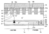
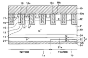
- an IGBT region 1a having an IGBT element and an FWD region 1b having an FWD element are formed on a common semiconductor substrate 10- It is said to be an IGBT.
- the portion on the collector layer 21 located on the other surface 10b of the semiconductor substrate 10 is defined as the IGBT region 1a, and the other surface 10b of the semiconductor substrate 10 is defined as the IGBT region 1a.
- the portion on the cathode layer 22 located at is defined as the FWD region 1b.
- the semiconductor device has a semiconductor substrate 10 that constitutes an N-type drift layer 11.
- the semiconductor substrate 10 of the present embodiment is made of a silicon substrate and has a thickness of about 127 ⁇ m.
- a base layer 12 is formed on the drift layer 11. That is, the base layer 12 is formed on the one side 10a side of the semiconductor substrate 10.
- a plurality of trenches 13 are formed in the semiconductor substrate 10 so as to penetrate the base layer 12 from the one side 10a side and reach the drift layer 11. As a result, the base layer 12 is separated into a plurality of pieces by the trench 13.
- the plurality of trenches 13 are formed in the IGBT region 1a and the FWD region 1b, respectively. Further, in the present embodiment, the plurality of trenches 13 are formed in a stripe shape with one direction intersecting the arrangement direction of the IGBT region 1a and the FWD region 1b as the longitudinal direction (that is, the paper surface depth direction in FIG. 1). ..
- Each trench 13 is embedded by a gate insulating film 14 formed so as to cover the wall surface of each trench 13 and a gate electrode 15 formed of polysilicon or the like formed on the gate insulating film 14. .. As a result, a trench gate structure is constructed.
- the gate electrode 15 formed in the IGBT region 1a is connected to a gate driver or the like via a gate pad or the like (not shown) so that a predetermined voltage is applied.
- the gate electrode 15 formed in the FWD region 1b is connected to the upper electrode 19 described later, and has the same potential as the upper electrode 19.
- an N + type emitter region 16 having a higher carrier concentration than the drift layer 11 is formed on the surface layer portion of the base layer 12. That is, an emitter region 16 is formed in the IGBT region 1a on the one side 10a side of the semiconductor substrate 10. Further, on the surface layer portion of the base layer 12, a P + type contact region 17 having a higher carrier concentration than that of the base layer 12 is formed in the IGBT region 1a. Specifically, the emitter region 16 is formed so as to be terminated in the base layer 12 and in contact with the side surface of the trench 13. Further, the contact region 17 is formed so as to be terminated in the base layer 12 and sandwiched between the two emitter regions 16.
- the emitter region 16 extends in a rod shape along the longitudinal direction of the trench 13 so as to be in contact with the side surface of the trench 13 in the region between the adjacent trenches 13, and terminates inside the tip of the trench 13. It is said to be a structure. Further, the contact region 17 extends in a rod shape along the longitudinal direction of the trench 13 so as to be in contact with the emitter region 16.
- the portion of the wall surface of the trench 13 located between the emitter region 16 and the drift layer 11 corresponds to the surface of the base layer located between the emitter region and the drift layer. Further, in the present embodiment, the contact region 17 is formed deeper than the emitter region 16.
- An interlayer insulating film 18 made of BPSG (abbreviation of Borophosphosilicate Glass) or the like is formed on one surface 10a of the semiconductor substrate 10.
- the interlayer insulating film 18 is formed with contact holes 18a that expose the emitter region 16 and the contact region 17 located between the adjacent trenches 13 in the IGBT region 1a of the one surface 10a of the semiconductor substrate 10. Further, in the interlayer insulating film 18, a contact hole 18b for exposing the base layer 12 is formed in the FWD region 1b of the one surface 10a of the semiconductor substrate 10, and a contact hole 18c for exposing the gate electrode 15 is formed. Has been done.
- the upper electrode 19 is formed on the interlayer insulating film 18.
- the upper electrode 19 is electrically connected to the emitter region 16 and the contact region 17 through the contact hole 18a formed in the interlayer insulating film 18.
- the upper electrode 19 is electrically connected to the base layer 12 through the contact hole 18b formed in the interlayer insulating film 18, and is gated through the contact hole 18c formed in the interlayer insulating film 18. It is electrically connected to the electrode 15.
- an upper electrode 19 that functions as an emitter electrode in the IGBT region 1a and functions as an anode electrode in the FWD region 1b is formed.
- the upper electrode 19 corresponds to the first electrode.
- An N-type field stop layer (hereinafter referred to as an FS layer) 20 having a higher carrier concentration than the drift layer 11 is formed on the side of the drift layer 11 opposite to the base layer 12 side. That is, the FS layer 20 is formed on the other surface 10b side of the semiconductor substrate 10.
- a P + type collector layer 21 is formed on the side opposite to the drift layer 11 across the FS layer 20, and in the FWD region 1b, N is formed on the side opposite to the drift layer 11 across the FS layer 20.
- a + -shaped cathode layer 22 is formed.
- the collector layer 21 is deeper than the cathode layer 22 from the other surface 10b of the semiconductor substrate 10 (hereinafter, also simply referred to as a depth).
- the collector layer 21 is configured to have an extension portion 21a extending above the cathode layer 22. That is, the collector layer 21 is configured to have an extending portion 21a that covers the portion of the cathode layer 22 on the drift layer 11 side.
- the extension portion 21a of the present embodiment is not formed in the entire region on the cathode layer 22, and the portion of the cathode layer 22 on the drift layer 11 side opposite to the collector layer 21 extends. It is in a state of being exposed from the installation portion 21a.
- the length of the extension portion 21a along the arrangement direction of the collector layer 21 and the cathode layer 22 is defined as the length x of the extension portion 21a.
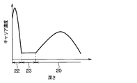
- connection region 23 is arranged between the portion of the cathode layer 22 exposed from the extending portion 21a and the FS layer 20.
- the connection region 23 has a lower carrier concentration than the cathode layer 22, and has the same carrier concentration as the drift layer 11. More specifically, the connecting region 23 is composed of a part of the drift layer 11.
- the FS layer 20, the collector layer 21, the cathode layer 22, and the connecting region 23 as described above are formed as follows, for example. That is, after ion-implanting the impurities constituting the FS layer 20, the impurities constituting the collector layer 21 including the extending portion 21a are ion-implanted. After that, impurities constituting the cathode layer 22 are ion-implanted between the portion constituting the extending portion 21a and the other surface 10b of the semiconductor substrate 10 and heat-treated.
- the carrier concentration is normal as shown in FIGS. 2A and 2B. It is a distribution. Since the connecting region 23 of the present embodiment is composed of a part of the drift layer 11, the carrier concentration is constant.
- the collector layer 21 and the cathode layer 22 are formed adjacent to each other.
- the IGBT region 1a and the FWD region 1b are partitioned by whether the layer located on the other surface 10b of the semiconductor substrate 10 is the collector layer 21 or the cathode layer 22. That is, in the present embodiment, the portion on the collector layer 21 located on the other surface 10b of the semiconductor substrate 10 is the IGBT region 1a, and the portion on the cathode layer 22 located on the other surface 10b of the semiconductor substrate 10 is the FWD region 1b. It is said that. Therefore, it can be said that the extension portion 21a of the present embodiment is formed in the FWD region 1b.
- a lower electrode 24 that is electrically connected to the collector layer 21 and the cathode layer 22 is formed on the side opposite to the drift layer 11 with the collector layer 21 and the cathode layer 22 interposed therebetween.
- the lower electrode 24 is formed on the other surface 10b of the semiconductor substrate 10. That is, a lower electrode 24 that functions as a collector electrode in the IGBT region 1a and a cathode electrode in the FWD region 1b is formed. In this embodiment, the lower electrode 24 corresponds to the second electrode.
- the semiconductor device of the present embodiment is configured in this way, and in the IGBT region 1a, an IGBT element having the base layer 12 as the base, the emitter region 16 as the emitter, and the collector layer 21 as the collector is configured. .. Further, in the FWD region 1b, a PN-junctioned FWD element is configured with the base layer as the anode and the drift layer 11, the FS layer 20, the cathode layer 22, and the connecting region 23 as the cathode.
- the N type, N + type, and N ⁇ type correspond to the first conductive type
- the P type and P + type correspond to the second conductive type.
- the semiconductor substrate 10 is configured as described above, so that the semiconductor substrate 10 includes a collector layer 21, a cathode layer 22, a connecting region 23, an FS layer 20, a drift layer 11, a base layer 12, and an emitter region 16.
- the configuration includes the contact area 17.
- the PN junction formed between the base layer 12 and the drift layer 11 becomes a reverse conduction state and a depletion layer is formed.
- a low level (for example, 0V) voltage lower than the threshold voltage Vth of the insulated gate structure is applied to the gate electrode 15, no current flows between the upper electrode 19 and the lower electrode 24.
- a high level voltage equal to or higher than the threshold voltage Vth of the insulated gate structure is applied to the gate electrode 15 in the IGBT region 1a while the lower electrode 24 is applied with a voltage higher than that of the upper electrode 19. Is applied.
- an inversion layer is formed in the portion of the base layer 12 in contact with the trench 13 in which the gate electrode 15 is arranged.
- electrons are supplied from the emitter region 16 to the drift layer 11 via the inversion layer, so that holes are supplied from the collector layer 21 to the drift layer 11, and the resistance value of the drift layer 11 is supplied by conductivity modulation. Turns on when the value decreases.
- the IGBT element when the IGBT element is turned off and the FWD element is turned on (that is, the FWD element is operated as a diode), the voltage applied to the upper electrode 19 and the lower electrode 24 is switched, and the lower electrode 19 is subjected to the lower voltage.
- a forward voltage is applied to apply a voltage higher than that of the electrode 24.
- holes are supplied to the base layer 12 and electrons are supplied to the cathode layer 22, so that the FWD element operates as a diode.
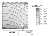
- the extending portion 21a is formed on the cathode layer 22. Therefore, when the IGBT element is turned on or the IGBT element is turned on, the electrons reach the portion of the FS layer 20 located in the IGBT region 1a, as shown in FIG. After that, it moves to the FWD region 1b side along the surface direction of the semiconductor substrate 10 and is discharged from the cathode layer 22. Then, the holes supplied from the collector layer 21 to the drift layer 11 are also supplied to the drift layer 11 from the extending portion 21a. Therefore, as shown in FIGS.
- FIG. 4B is a simulation result in which the length x of the extending portion 21a is the same as the width of the cathode layer 22, assuming that the arrangement direction of the IGBT region 1a and the FWD region 1b in the cathode layer 22 is the width of the cathode layer 22. be. That is, FIG. 4B is a simulation result when the extension portion 21a is arranged so as to cover the entire region on the cathode layer 22. However, even if the extension portion 21a is not arranged so as to cover the entire region on the cathode layer 22 as in the present embodiment, holes are also supplied to the drift layer 11 from the extension portion 21a, so that the IGBT is used. The hole concentration at the boundary between the region 1a and the FWD region 1b can be increased.
- the extension portion 21a in FIGS. 5A and 5B is a simulation result when the extension portion 21a is arranged so as to cover the entire region on the cathode layer 22.
- the hole concentration at the boundary between the IGBT region 1a and the FWD region 1b can be adjusted as described above. Since it can be made higher, it is possible to suppress the occurrence of snapback.
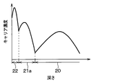
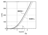
- FIG. 6 shows a simulation result in which the width of the cathode layer 22 is 24 ⁇ m, and the extension portion 21a is in a state of being arranged in the entire region on the cathode layer 22 when the length is 24 ⁇ m.
- the extension portion 21a is not formed so as to cover the entire region on the cathode layer 22, and a part of the cathode layer 22 is exposed from the extension portion 21a. It has become. That is, the length x of the extended portion 21a is less than 24 ⁇ m. Therefore, as shown in FIG. 6, it is possible to suppress an increase in the forward voltage of the FWD element.
- FIG. 6 is a simulation result when a current of 400 A is passed at 150 ° C., and the on voltage is shown as Von and the forward voltage is shown as Vf. Then, as shown in FIG. 6, the on-voltage becomes lower as the length x of the extending portion 21a becomes longer. Therefore, it is preferable that a part of the cathode layer 22 of the extension portion 21a is exposed from the extension portion 21a and the length x is set according to the required on-voltage and the like. For example, in the present embodiment, when the length x is 23 ⁇ m, it is possible to sufficiently reduce the on-voltage and suppress the increase in the forward voltage. That is, when the ratio of the length x of the extending portion 21a to the width of the cathode layer 22 is 23/24, it is possible to sufficiently reduce the on-voltage and suppress the increase in the forward voltage.
- the carrier concentration of the connecting region 23 between the FS layer 20 and the cathode layer 22 is lower than that of the cathode layer 22. Therefore, for example, the portion exposed from the extending portion 21a on the cathode layer 22 is applied to the PN junction between the collector layer 21 and the FS layer 20 as compared with the case where the portion exposed from the extending portion 21a is connected to the FS layer 20.
- the voltage can be increased. Therefore, when the IGBT element is in the ON state, the holes supplied to the collector layer 21 can be increased, and the extension portion 21a is turned on because the extension portion 21a is not arranged in the entire region on the cathode layer 22. It is possible to suppress an increase in voltage.
- the extension portion 21a is formed so as to cover a part of the cathode layer 22. Therefore, it is possible to suppress snapback when the IGBT element is turned on.
- the cathode layer 22 has a portion exposed from the extending portion 21a. Therefore, when the FWD element is in the ON state, it is possible to suppress the difficulty of electrons moving from the cathode layer 22 to the base layer 12 side, and it is possible to suppress an increase in the forward voltage.
- a connecting region 23 having a lower carrier concentration than the cathode layer 22 is arranged between the FS layer 20 and the cathode layer 22. Therefore, for example, the portion exposed from the extending portion 21a on the cathode layer 22 is applied to the PN junction between the collector layer 21 and the FS layer 20 as compared with the case where the portion exposed from the extending portion 21a is connected to the FS layer 20.
- the voltage can be increased. Therefore, when the IGBT element is in the ON state, the holes supplied to the collector layer 21 can be increased, and the extension portion 21a is turned on because the extension portion 21a is not arranged in the entire region on the cathode layer 22. It is possible to suppress an increase in voltage.
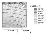
- the extension portion 21a is formed in the entire region on the cathode layer 22. That is, the cathode layer 22 is in a state where the entire region on the drift layer 11 side is covered with the extending portion 21a. Therefore, in the semiconductor device of the present embodiment, as described above, the forward voltage of the FWD element may increase. Therefore, in the semiconductor device of the present embodiment, the extension portion 21a has the following configuration. Hereinafter, the configuration of the extension portion 21a in the present embodiment will be described with reference to FIGS. 8 to 10. In FIGS.
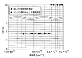
- the depth of the cathode layer 22 is set to 0.15 ⁇ m with the other surface 10b of the semiconductor substrate 10 as a reference for the depth, and the depth of the collector layer 21 is set to the depth as shown in FIG. Let d. Further, in FIGS. 8 to 10, the forward voltage of the FWD element is shown as Vf.
- the forward voltage of the FWD element is such that the depth d of the collector layer 21 is 0.5 ⁇ m. It is confirmed that the number increases sharply when the above is reached. Further, as shown in FIG. 9, when the depth d of the collector layer 21 is fixed at 0.5 ⁇ m, the forward voltage of the FWD element is such that the carrier concentration of the collector layer 21 is 1.0 ⁇ 10 17 cm -3. It is confirmed that the number increases sharply when the above is reached. 8 and 9 are simulation results when the carrier concentration is constant along the depth direction.
- the extension portion 21a has a surface density of 3.5 ⁇ 10 12 cm- 2 or less.
- the extension portion 21a is formed in the entire region on the cathode layer 22. Therefore, it is possible to suppress snapback when the IGBT element is turned on.
- the surface density of the extended portion 21a is 3.5 ⁇ 10 12 cm- 2 or less. Therefore, it is possible to suppress an increase in the forward voltage of the FWD element.
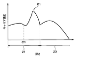
- the basic configuration of the semiconductor device of the present embodiment is the same as that of the first embodiment, but the collector layer 21 is configured so that the carrier concentration has a plurality of peaks as shown in FIG. There is. Then, in the collector layer 21, the maximum peak position P1 at which the carrier concentration is maximum is located in the drift layer 11 (that is, on the FS layer 20 side) of the center C1 of the collector layer 21 in the depth direction of the semiconductor substrate 10. Is formed in.
- Such a collector layer 21 is formed, for example, by performing a plurality of ion implantations in which the acceleration voltage is changed.
- the maximum peak position P1 of the collector layer 21 is located closer to the drift layer 11 than the center C1. Therefore, it is possible to suppress the occurrence of avalanche yield and improve SCSOA (abbreviation of Short Circuit Safe Operating Area).
- SCSOA abbreviation of Short Circuit Safe Operating Area
- the electric field strength becomes a state in which a peak is generated on the other surface 10b side of the semiconductor substrate 10 because the number of holes injected is reduced and the number of electrons is excessive.
- the FS layer 20 since the FS layer 20 is formed, a peak occurs in the FS layer 20. Then, in the semiconductor device, when the peak of the electric field strength is on the lower electrode 24 side, avalanche breakdown is likely to occur.
- the maximum peak position P1 of the carrier concentration of the collector layer 21 is set to the drift layer 11 side. Therefore, for example, as compared with the case where the maximum peak position P1 is located on the other surface 10b side of the semiconductor substrate 10 with respect to the center C1, the number of holes injected at the position where the electric field strength can be the peak at the time of a short circuit is increased. It becomes easy to do so, and the excess state of electrons can be alleviated. Therefore, it is possible to suppress the occurrence of avalanche yield.
- the first conductive type is N type and the second conductive type is P type has been described, but the first conductive type is P type and the second conductive type is N type. You can also do it.
- each of the above embodiments may be a planar type semiconductor device in which the gate electrode 15 is arranged on one surface 10a of the semiconductor substrate 10 instead of the trench gate type semiconductor device.
- the configuration on the one side 10a side of the semiconductor substrate 10 in the FWD region 1b can be changed as appropriate.
- an N-type region or the like corresponding to the emitter region 16 may be formed on one surface 10a side of the semiconductor substrate 10 in the FWD region 1b.
- the portion of the cathode layer 22 exposed from the extending portion 21a may be connected to the FS layer 20. Further, the connection region 23 may have a higher carrier concentration than the cathode layer 22. Even in such a semiconductor device, the cathode layer 22 is configured to have a portion exposed from the extending portion 21a, thereby suppressing the snapback of the IGBT element and suppressing the increase in the forward voltage of the FWD element. can.
- each of the above embodiments can be combined as appropriate.
- the second embodiment may be combined with the third embodiment so that the maximum peak position P1 of the collector layer 21 is closer to the drift layer 11 than the center C1.
Landscapes
- Insulated Gate Type Field-Effect Transistor (AREA)
- Electrodes Of Semiconductors (AREA)
- Metal-Oxide And Bipolar Metal-Oxide Semiconductor Integrated Circuits (AREA)
Priority Applications (3)
| Application Number | Priority Date | Filing Date | Title |
|---|---|---|---|
| CN202180030791.0A CN115485857A (zh) | 2020-04-28 | 2021-04-23 | 半导体装置 |
| US17/972,945 US12363997B2 (en) | 2020-04-28 | 2022-10-25 | Semiconductor device |
| US19/231,815 US20250301773A1 (en) | 2020-04-28 | 2025-06-09 | Semiconductor device |
Applications Claiming Priority (2)
| Application Number | Priority Date | Filing Date | Title |
|---|---|---|---|
| JP2020079269A JP7435214B2 (ja) | 2020-04-28 | 2020-04-28 | 半導体装置 |
| JP2020-079269 | 2020-04-28 |
Related Child Applications (1)
| Application Number | Title | Priority Date | Filing Date |
|---|---|---|---|
| US17/972,945 Continuation US12363997B2 (en) | 2020-04-28 | 2022-10-25 | Semiconductor device |
Publications (1)
| Publication Number | Publication Date |
|---|---|
| WO2021220965A1 true WO2021220965A1 (ja) | 2021-11-04 |
Family
ID=78278327
Family Applications (1)
| Application Number | Title | Priority Date | Filing Date |
|---|---|---|---|
| PCT/JP2021/016486 Ceased WO2021220965A1 (ja) | 2020-04-28 | 2021-04-23 | 半導体装置 |
Country Status (4)
| Country | Link |
|---|---|
| US (2) | US12363997B2 (enExample) |
| JP (1) | JP7435214B2 (enExample) |
| CN (1) | CN115485857A (enExample) |
| WO (1) | WO2021220965A1 (enExample) |
Cited By (1)
| Publication number | Priority date | Publication date | Assignee | Title |
|---|---|---|---|---|
| WO2024219041A1 (ja) * | 2023-04-18 | 2024-10-24 | 株式会社デンソー | 半導体装置とその製造方法 |
Families Citing this family (4)
| Publication number | Priority date | Publication date | Assignee | Title |
|---|---|---|---|---|
| JP7729175B2 (ja) | 2021-10-26 | 2025-08-26 | 住友ゴム工業株式会社 | タイヤ |
| JP7692875B2 (ja) * | 2022-05-16 | 2025-06-16 | 三菱電機株式会社 | パワー半導体装置およびパワー半導体装置の製造方法 |
| JP2024080317A (ja) * | 2022-12-02 | 2024-06-13 | 株式会社デンソー | 半導体装置とその製造方法 |
| JP2024162687A (ja) * | 2023-05-11 | 2024-11-21 | 株式会社デンソー | 半導体装置とその製造方法 |
Citations (6)
| Publication number | Priority date | Publication date | Assignee | Title |
|---|---|---|---|---|
| JP2003303965A (ja) * | 2002-04-09 | 2003-10-24 | Toshiba Corp | 半導体素子及びその製造方法 |
| JP2007012972A (ja) * | 2005-07-01 | 2007-01-18 | Shindengen Electric Mfg Co Ltd | 半導体装置及びその製造方法 |
| JP2016086136A (ja) * | 2014-10-29 | 2016-05-19 | トヨタ自動車株式会社 | 半導体装置の製造方法 |
| JP6158123B2 (ja) * | 2014-03-14 | 2017-07-05 | 株式会社東芝 | 半導体装置 |
| WO2019176810A1 (ja) * | 2018-03-15 | 2019-09-19 | 富士電機株式会社 | 半導体装置 |
| JP2020004824A (ja) * | 2018-06-27 | 2020-01-09 | 三菱電機株式会社 | 半導体装置、半導体装置の製造方法 |
Family Cites Families (1)
| Publication number | Priority date | Publication date | Assignee | Title |
|---|---|---|---|---|
| JP5937413B2 (ja) * | 2011-06-15 | 2016-06-22 | 株式会社デンソー | 半導体装置 |
-
2020
- 2020-04-28 JP JP2020079269A patent/JP7435214B2/ja active Active
-
2021
- 2021-04-23 CN CN202180030791.0A patent/CN115485857A/zh active Pending
- 2021-04-23 WO PCT/JP2021/016486 patent/WO2021220965A1/ja not_active Ceased
-
2022
- 2022-10-25 US US17/972,945 patent/US12363997B2/en active Active
-
2025
- 2025-06-09 US US19/231,815 patent/US20250301773A1/en active Pending
Patent Citations (6)
| Publication number | Priority date | Publication date | Assignee | Title |
|---|---|---|---|---|
| JP2003303965A (ja) * | 2002-04-09 | 2003-10-24 | Toshiba Corp | 半導体素子及びその製造方法 |
| JP2007012972A (ja) * | 2005-07-01 | 2007-01-18 | Shindengen Electric Mfg Co Ltd | 半導体装置及びその製造方法 |
| JP6158123B2 (ja) * | 2014-03-14 | 2017-07-05 | 株式会社東芝 | 半導体装置 |
| JP2016086136A (ja) * | 2014-10-29 | 2016-05-19 | トヨタ自動車株式会社 | 半導体装置の製造方法 |
| WO2019176810A1 (ja) * | 2018-03-15 | 2019-09-19 | 富士電機株式会社 | 半導体装置 |
| JP2020004824A (ja) * | 2018-06-27 | 2020-01-09 | 三菱電機株式会社 | 半導体装置、半導体装置の製造方法 |
Cited By (1)
| Publication number | Priority date | Publication date | Assignee | Title |
|---|---|---|---|---|
| WO2024219041A1 (ja) * | 2023-04-18 | 2024-10-24 | 株式会社デンソー | 半導体装置とその製造方法 |
Also Published As
| Publication number | Publication date |
|---|---|
| US20230037409A1 (en) | 2023-02-09 |
| JP7435214B2 (ja) | 2024-02-21 |
| US12363997B2 (en) | 2025-07-15 |
| CN115485857A (zh) | 2022-12-16 |
| US20250301773A1 (en) | 2025-09-25 |
| JP2021174924A (ja) | 2021-11-01 |
Similar Documents
| Publication | Publication Date | Title |
|---|---|---|
| CN109964317B (zh) | 半导体装置 | |
| KR100723594B1 (ko) | 역도통형 반도체소자와 그것의 제조방법 | |
| JP5605073B2 (ja) | 半導体装置 | |
| JP7435214B2 (ja) | 半導体装置 | |
| CN107210299B (zh) | 半导体装置 | |
| JP6445952B2 (ja) | 半導体装置 | |
| JP2019169597A (ja) | 半導体装置 | |
| US20140231865A1 (en) | Insulated gate semiconductor device and method for manufacturing the same | |
| JP6353804B2 (ja) | 半導体装置及びそれを用いた電力変換装置 | |
| WO2017199679A1 (ja) | 半導体装置 | |
| CN112673466A (zh) | 半导体装置 | |
| JP7247930B2 (ja) | 半導体装置 | |
| CN108365007B (zh) | 绝缘栅双极型晶体管 | |
| CN112689902B (zh) | 半导体装置 | |
| WO2016114131A1 (ja) | 半導体装置 | |
| WO2021045116A1 (ja) | 半導体装置 | |
| WO2019098122A1 (ja) | 半導体装置 | |
| JP7338242B2 (ja) | 半導体装置 | |
| JP6987015B2 (ja) | 半導体装置 | |
| JP2009246037A (ja) | 横型半導体装置 | |
| JP7596930B2 (ja) | 半導体装置 | |
| WO2025023245A1 (ja) | 半導体装置 | |
| KR100241055B1 (ko) | 트렌치-게이트 수평형 절연게이트 바이폴라 트랜지스터 | |
| JP2010251627A (ja) | 横型半導体装置 | |
| JP2025104940A (ja) | 半導体装置 |
Legal Events
| Date | Code | Title | Description |
|---|---|---|---|
| 121 | Ep: the epo has been informed by wipo that ep was designated in this application |
Ref document number: 21795641 Country of ref document: EP Kind code of ref document: A1 |
|
| NENP | Non-entry into the national phase |
Ref country code: DE |
|
| 122 | Ep: pct application non-entry in european phase |
Ref document number: 21795641 Country of ref document: EP Kind code of ref document: A1 |