WO2021193823A1 - 半導体装置およびその製造方法 - Google Patents
半導体装置およびその製造方法 Download PDFInfo
- Publication number
- WO2021193823A1 WO2021193823A1 PCT/JP2021/012535 JP2021012535W WO2021193823A1 WO 2021193823 A1 WO2021193823 A1 WO 2021193823A1 JP 2021012535 W JP2021012535 W JP 2021012535W WO 2021193823 A1 WO2021193823 A1 WO 2021193823A1
- Authority
- WO
- WIPO (PCT)
- Prior art keywords
- solder
- insulating substrate
- semiconductor element
- electrode plate
- main terminal
- Prior art date
- Legal status (The legal status is an assumption and is not a legal conclusion. Google has not performed a legal analysis and makes no representation as to the accuracy of the status listed.)
- Ceased
Links
Images











Classifications
-
- H—ELECTRICITY
- H10—SEMICONDUCTOR DEVICES; ELECTRIC SOLID-STATE DEVICES NOT OTHERWISE PROVIDED FOR
- H10W—GENERIC PACKAGES, INTERCONNECTIONS, CONNECTORS OR OTHER CONSTRUCTIONAL DETAILS OF DEVICES COVERED BY CLASS H10
- H10W76/00—Containers; Fillings or auxiliary members therefor; Seals
- H10W76/10—Containers or parts thereof
- H10W76/12—Containers or parts thereof characterised by their shape
- H10W76/15—Containers comprising an insulating or insulated base
-
- H—ELECTRICITY
- H10—SEMICONDUCTOR DEVICES; ELECTRIC SOLID-STATE DEVICES NOT OTHERWISE PROVIDED FOR
- H10W—GENERIC PACKAGES, INTERCONNECTIONS, CONNECTORS OR OTHER CONSTRUCTIONAL DETAILS OF DEVICES COVERED BY CLASS H10
- H10W70/00—Package substrates; Interposers; Redistribution layers [RDL]
- H10W70/60—Insulating or insulated package substrates; Interposers; Redistribution layers
- H10W70/67—Insulating or insulated package substrates; Interposers; Redistribution layers characterised by their insulating layers or insulating parts
- H10W70/69—Insulating materials thereof
- H10W70/692—Ceramics or glasses
-
- H—ELECTRICITY
- H10—SEMICONDUCTOR DEVICES; ELECTRIC SOLID-STATE DEVICES NOT OTHERWISE PROVIDED FOR
- H10W—GENERIC PACKAGES, INTERCONNECTIONS, CONNECTORS OR OTHER CONSTRUCTIONAL DETAILS OF DEVICES COVERED BY CLASS H10
- H10W40/00—Arrangements for thermal protection or thermal control
- H10W40/20—Arrangements for cooling
- H10W40/22—Arrangements for cooling characterised by their shape, e.g. having conical or cylindrical projections
- H10W40/226—Arrangements for cooling characterised by their shape, e.g. having conical or cylindrical projections characterised by projecting parts, e.g. fins to increase surface area
- H10W40/228—Arrangements for cooling characterised by their shape, e.g. having conical or cylindrical projections characterised by projecting parts, e.g. fins to increase surface area the projecting parts being wire-shaped or pin-shaped
-
- H—ELECTRICITY
- H10—SEMICONDUCTOR DEVICES; ELECTRIC SOLID-STATE DEVICES NOT OTHERWISE PROVIDED FOR
- H10W—GENERIC PACKAGES, INTERCONNECTIONS, CONNECTORS OR OTHER CONSTRUCTIONAL DETAILS OF DEVICES COVERED BY CLASS H10
- H10W40/00—Arrangements for thermal protection or thermal control
- H10W40/20—Arrangements for cooling
- H10W40/25—Arrangements for cooling characterised by their materials
- H10W40/255—Arrangements for cooling characterised by their materials having a laminate or multilayered structure, e.g. direct bond copper [DBC] ceramic substrates
-
- H—ELECTRICITY
- H10—SEMICONDUCTOR DEVICES; ELECTRIC SOLID-STATE DEVICES NOT OTHERWISE PROVIDED FOR
- H10W—GENERIC PACKAGES, INTERCONNECTIONS, CONNECTORS OR OTHER CONSTRUCTIONAL DETAILS OF DEVICES COVERED BY CLASS H10
- H10W74/00—Encapsulations, e.g. protective coatings
- H10W74/10—Encapsulations, e.g. protective coatings characterised by their shape or disposition
- H10W74/111—Encapsulations, e.g. protective coatings characterised by their shape or disposition the semiconductor body being completely enclosed
- H10W74/114—Encapsulations, e.g. protective coatings characterised by their shape or disposition the semiconductor body being completely enclosed by a substrate and the encapsulations
- H10W74/117—Encapsulations, e.g. protective coatings characterised by their shape or disposition the semiconductor body being completely enclosed by a substrate and the encapsulations the substrate having spherical bumps for external connection
-
- H—ELECTRICITY
- H10—SEMICONDUCTOR DEVICES; ELECTRIC SOLID-STATE DEVICES NOT OTHERWISE PROVIDED FOR
- H10W—GENERIC PACKAGES, INTERCONNECTIONS, CONNECTORS OR OTHER CONSTRUCTIONAL DETAILS OF DEVICES COVERED BY CLASS H10
- H10W90/00—Package configurations
-
- H—ELECTRICITY
- H10—SEMICONDUCTOR DEVICES; ELECTRIC SOLID-STATE DEVICES NOT OTHERWISE PROVIDED FOR
- H10W—GENERIC PACKAGES, INTERCONNECTIONS, CONNECTORS OR OTHER CONSTRUCTIONAL DETAILS OF DEVICES COVERED BY CLASS H10
- H10W70/00—Package substrates; Interposers; Redistribution layers [RDL]
- H10W70/40—Leadframes
- H10W70/481—Leadframes for devices being provided for in groups H10D8/00 - H10D48/00
-
- H—ELECTRICITY
- H10—SEMICONDUCTOR DEVICES; ELECTRIC SOLID-STATE DEVICES NOT OTHERWISE PROVIDED FOR
- H10W—GENERIC PACKAGES, INTERCONNECTIONS, CONNECTORS OR OTHER CONSTRUCTIONAL DETAILS OF DEVICES COVERED BY CLASS H10
- H10W72/00—Interconnections or connectors in packages
- H10W72/071—Connecting or disconnecting
- H10W72/073—Connecting or disconnecting of die-attach connectors
-
- H—ELECTRICITY
- H10—SEMICONDUCTOR DEVICES; ELECTRIC SOLID-STATE DEVICES NOT OTHERWISE PROVIDED FOR
- H10W—GENERIC PACKAGES, INTERCONNECTIONS, CONNECTORS OR OTHER CONSTRUCTIONAL DETAILS OF DEVICES COVERED BY CLASS H10
- H10W72/00—Interconnections or connectors in packages
- H10W72/50—Bond wires
- H10W72/521—Structures or relative sizes of bond wires
- H10W72/522—Multilayered bond wires, e.g. having a coating concentric around a core
-
- H—ELECTRICITY
- H10—SEMICONDUCTOR DEVICES; ELECTRIC SOLID-STATE DEVICES NOT OTHERWISE PROVIDED FOR
- H10W—GENERIC PACKAGES, INTERCONNECTIONS, CONNECTORS OR OTHER CONSTRUCTIONAL DETAILS OF DEVICES COVERED BY CLASS H10
- H10W72/00—Interconnections or connectors in packages
- H10W72/50—Bond wires
- H10W72/531—Shapes of wire connectors
- H10W72/5363—Shapes of wire connectors the connected ends being wedge-shaped
-
- H—ELECTRICITY
- H10—SEMICONDUCTOR DEVICES; ELECTRIC SOLID-STATE DEVICES NOT OTHERWISE PROVIDED FOR
- H10W—GENERIC PACKAGES, INTERCONNECTIONS, CONNECTORS OR OTHER CONSTRUCTIONAL DETAILS OF DEVICES COVERED BY CLASS H10
- H10W72/00—Interconnections or connectors in packages
- H10W72/50—Bond wires
- H10W72/551—Materials of bond wires
- H10W72/552—Materials of bond wires comprising metals or metalloids, e.g. silver
- H10W72/5522—Materials of bond wires comprising metals or metalloids, e.g. silver comprising gold [Au]
-
- H—ELECTRICITY
- H10—SEMICONDUCTOR DEVICES; ELECTRIC SOLID-STATE DEVICES NOT OTHERWISE PROVIDED FOR
- H10W—GENERIC PACKAGES, INTERCONNECTIONS, CONNECTORS OR OTHER CONSTRUCTIONAL DETAILS OF DEVICES COVERED BY CLASS H10
- H10W72/00—Interconnections or connectors in packages
- H10W72/50—Bond wires
- H10W72/551—Materials of bond wires
- H10W72/552—Materials of bond wires comprising metals or metalloids, e.g. silver
- H10W72/5524—Materials of bond wires comprising metals or metalloids, e.g. silver comprising aluminium [Al]
-
- H—ELECTRICITY
- H10—SEMICONDUCTOR DEVICES; ELECTRIC SOLID-STATE DEVICES NOT OTHERWISE PROVIDED FOR
- H10W—GENERIC PACKAGES, INTERCONNECTIONS, CONNECTORS OR OTHER CONSTRUCTIONAL DETAILS OF DEVICES COVERED BY CLASS H10
- H10W72/00—Interconnections or connectors in packages
- H10W72/50—Bond wires
- H10W72/551—Materials of bond wires
- H10W72/552—Materials of bond wires comprising metals or metalloids, e.g. silver
- H10W72/5525—Materials of bond wires comprising metals or metalloids, e.g. silver comprising copper [Cu]
-
- H—ELECTRICITY
- H10—SEMICONDUCTOR DEVICES; ELECTRIC SOLID-STATE DEVICES NOT OTHERWISE PROVIDED FOR
- H10W—GENERIC PACKAGES, INTERCONNECTIONS, CONNECTORS OR OTHER CONSTRUCTIONAL DETAILS OF DEVICES COVERED BY CLASS H10
- H10W72/00—Interconnections or connectors in packages
- H10W72/50—Bond wires
- H10W72/551—Materials of bond wires
- H10W72/555—Materials of bond wires of outermost layers of multilayered bond wires, e.g. material of a coating
-
- H—ELECTRICITY
- H10—SEMICONDUCTOR DEVICES; ELECTRIC SOLID-STATE DEVICES NOT OTHERWISE PROVIDED FOR
- H10W—GENERIC PACKAGES, INTERCONNECTIONS, CONNECTORS OR OTHER CONSTRUCTIONAL DETAILS OF DEVICES COVERED BY CLASS H10
- H10W74/00—Encapsulations, e.g. protective coatings
-
- H—ELECTRICITY
- H10—SEMICONDUCTOR DEVICES; ELECTRIC SOLID-STATE DEVICES NOT OTHERWISE PROVIDED FOR
- H10W—GENERIC PACKAGES, INTERCONNECTIONS, CONNECTORS OR OTHER CONSTRUCTIONAL DETAILS OF DEVICES COVERED BY CLASS H10
- H10W74/00—Encapsulations, e.g. protective coatings
- H10W74/40—Encapsulations, e.g. protective coatings characterised by their materials
- H10W74/47—Encapsulations, e.g. protective coatings characterised by their materials comprising organic materials, e.g. plastics or resins
- H10W74/473—Encapsulations, e.g. protective coatings characterised by their materials comprising organic materials, e.g. plastics or resins containing a filler
-
- H—ELECTRICITY
- H10—SEMICONDUCTOR DEVICES; ELECTRIC SOLID-STATE DEVICES NOT OTHERWISE PROVIDED FOR
- H10W—GENERIC PACKAGES, INTERCONNECTIONS, CONNECTORS OR OTHER CONSTRUCTIONAL DETAILS OF DEVICES COVERED BY CLASS H10
- H10W76/00—Containers; Fillings or auxiliary members therefor; Seals
- H10W76/40—Fillings or auxiliary members in containers, e.g. centering rings
- H10W76/42—Fillings
- H10W76/47—Solid or gel fillings
-
- H—ELECTRICITY
- H10—SEMICONDUCTOR DEVICES; ELECTRIC SOLID-STATE DEVICES NOT OTHERWISE PROVIDED FOR
- H10W—GENERIC PACKAGES, INTERCONNECTIONS, CONNECTORS OR OTHER CONSTRUCTIONAL DETAILS OF DEVICES COVERED BY CLASS H10
- H10W90/00—Package configurations
- H10W90/701—Package configurations characterised by the relative positions of pads or connectors relative to package parts
-
- H—ELECTRICITY
- H10—SEMICONDUCTOR DEVICES; ELECTRIC SOLID-STATE DEVICES NOT OTHERWISE PROVIDED FOR
- H10W—GENERIC PACKAGES, INTERCONNECTIONS, CONNECTORS OR OTHER CONSTRUCTIONAL DETAILS OF DEVICES COVERED BY CLASS H10
- H10W90/00—Package configurations
- H10W90/701—Package configurations characterised by the relative positions of pads or connectors relative to package parts
- H10W90/731—Package configurations characterised by the relative positions of pads or connectors relative to package parts of die-attach connectors
- H10W90/734—Package configurations characterised by the relative positions of pads or connectors relative to package parts of die-attach connectors between a chip and a stacked insulating package substrate, interposer or RDL
-
- H—ELECTRICITY
- H10—SEMICONDUCTOR DEVICES; ELECTRIC SOLID-STATE DEVICES NOT OTHERWISE PROVIDED FOR
- H10W—GENERIC PACKAGES, INTERCONNECTIONS, CONNECTORS OR OTHER CONSTRUCTIONAL DETAILS OF DEVICES COVERED BY CLASS H10
- H10W90/00—Package configurations
- H10W90/701—Package configurations characterised by the relative positions of pads or connectors relative to package parts
- H10W90/761—Package configurations characterised by the relative positions of pads or connectors relative to package parts of strap connectors
- H10W90/763—Package configurations characterised by the relative positions of pads or connectors relative to package parts of strap connectors between laterally-adjacent chips
Definitions
- This disclosure relates to a semiconductor device and a method for manufacturing the same.
- So-called power modules as semiconductor devices are becoming widespread in all products from industrial equipment to home appliances and information terminals. High reliability is required for power modules installed in electric vehicles. It is also necessary that the power module for an electric vehicle has a high operating temperature and excellent efficiency. Therefore, the power module for electric vehicles is also required to have a package form applicable to silicon carbide semiconductors, which are likely to become mainstream in the future.
- Patent Document 1 Japanese Patent Application Laid-Open No. 2016-058563
- the thickness of the sealing resin and the coefficient of linear expansion are adjusted so as to be in an appropriate numerical range.
- the insulating substrate is given a downwardly convex warp, and air is prevented from being caught in the heat radiating grease portion between the heat radiating member and the insulating substrate.
- a wire tool is used when wire bonding wiring for circuit formation to a semiconductor element on the insulating substrate.
- the way of hitting changes. That is, when a plurality of semiconductor elements are mounted on the insulating substrate, the inclination angle of the surface of the semiconductor element with respect to the horizontal direction differs depending on the location of the plurality of semiconductor elements. This causes the need to readjust the way the wire tool hits during wire bonding for each of the plurality of semiconductor elements. Therefore, for example, if the adjustment is insufficient, the wire tool may damage the semiconductor element, and it may be difficult to wire-bond the wiring with high reliability.
- An object of the present invention is to provide a semiconductor device having high reliability in which a circuit is stably connected to a semiconductor element mounted on an insulating substrate having a curved main surface and a method for manufacturing the same.
- the semiconductor device of this embodiment includes an insulating substrate, a heat radiating member, and an electrode plate.
- a semiconductor element is mounted on the insulating substrate.
- the heat radiating member is joined to the insulating substrate by the first solder.
- the electrode plate is arranged so as to overlap at least a part of the semiconductor element.
- the main surface of the insulating substrate is warped so as to have a convex shape on the heat radiating member side.
- the first solder is thicker at the edges than at the center in plan view.
- the semiconductor element is joined to the electrode plate by a second solder.
- the heat radiating member and the insulating substrate are joined by the first solder.
- a semiconductor element is bonded to the insulating substrate.
- the electrode plate that overlaps at least a part of the semiconductor element is joined to the semiconductor element by the second solder.
- the insulating substrate is joined to the heat radiating member so that the main surface warps so as to have a convex shape toward the heat radiating member side.
- the first solder is formed so as to be thicker at the edges than at the center in plan view.
- FIG. 1 It is schematic cross-sectional view which shows the structure of the power module which concerns on Embodiment 1.
- FIG. It is schematic cross-sectional view which shows the 1st modification of the structure of the power module which concerns on Embodiment 1.
- FIG. It is schematic cross-sectional view which shows the 2nd modification of the structure of the power module which concerns on Embodiment 1.
- FIG. It is schematic cross-sectional view which shows the 3rd modification of the structure of the power module which concerns on Embodiment 1.
- FIG. It is schematic cross-sectional view which shows the 4th modification of the structure of the power module which concerns on Embodiment 1.
- FIG. It is schematic cross-sectional view which shows the 5th modification of the structure of the power module which concerns on Embodiment 1.
- FIG. 1 It is schematic cross-sectional view which shows the 2nd step of the manufacturing method of the power module which concerns on FIG. 1 of Embodiment 1.
- FIG. It is a schematic cross-sectional view which shows the 3rd process of the manufacturing method of the power module which concerns on FIG. 1 of Embodiment 1.
- FIG. It is schematic cross-sectional view which shows the structure of the power module which concerns on Embodiment 2.
- FIG. It is schematic cross-sectional view which shows the structure of the power module which concerns on Embodiment 3.
- FIG. It is a schematic cross-sectional view which shows the 1st process of the manufacturing method of the power module which concerns on Embodiment 3.
- FIG. It is a schematic cross-sectional view which shows the 3rd process of the manufacturing method of the power module which concerns on Embodiment 3.
- FIG. It is a schematic cross-sectional view which shows the 4th process of the manufacturing method of the power module which concerns on Embodiment 3.
- FIG. It is schematic cross-sectional view which shows the structure of the power module which concerns on Embodiment 4.
- FIG. It is a schematic cross-sectional view which shows the 1st process of the manufacturing method of the power module which concerns on Embodiment 4.
- FIG. It is schematic cross-sectional view which shows the 2nd step of the manufacturing method of the power module which concerns on Embodiment 4.
- FIG. It is schematic cross-sectional view which shows the structure of the power module which concerns on Embodiment 5.
- the power module 100 as a semiconductor device according to the present embodiment will be described with reference to the drawings.
- the X direction, the Y direction, and the Z direction are introduced.
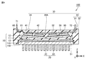
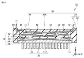
- FIG. 1 is a schematic cross-sectional view showing the configuration of the power module according to the first embodiment.
- the power module 100 of the present embodiment mainly includes an insulating substrate 10, a heat radiating member 20, and an electrode plate 30.
- the insulating substrate 10 includes a base material 11, a conductor layer 12, and a conductor layer 13.
- the base material 11 has, for example, a rectangular shape in a plan view, and has a thickness along the Z direction.
- the base material 11 has one surface 11A as the upper main surface in the Z direction and the other surface 11B as the lower main surface in the opposite side, that is, the Z direction.
- the conductor layer 12 is a thin plate-shaped conductor material bonded one or more on one surface 11A.
- the conductor layer 13 is a thin plate-shaped conductor material bonded one or more on the other surface 11B.
- the main surface of the insulating substrate 10 means a surface along the XY plane of the entire one in which the thin conductor layer 12 and the thin conductor layer 13 are joined to one surface 11A and the other surface 11B. Therefore, the main surface of the insulating substrate 10 extends so as to face substantially the same direction as the one surface 11A and the other surface 11B. Therefore, in the following, the main surface of the entire insulating substrate 10 may be regarded as the same as one surface 11A and the other surface 11B.
- An IGBT 41 (Integrated Gate Bipolar Transistor) and a diode 42 as semiconductor elements are mounted on the conductor layer 12 of the insulating substrate 10. These semiconductor elements are chip-shaped. Normally, as shown in FIG. 1, the IGBT 41 as the second semiconductor element is arranged outside the diode 42 as the first semiconductor element in a plan view. However, the present invention is not limited to this, and the IGBT 41 may be arranged inside the diode 42 in a plan view.
- the heat radiating member 20 includes a base plate 21 and fins 22.
- the base plate 21 is a plate-shaped member having a surface along the XY plane.
- the fin 22 is a member extending along the Z direction from the lowermost surface of the base plate 21 in the Z direction, for example.
- a plurality of fins 22 extend downward in the Z direction from the lowermost surface of the base plate 21 at intervals in the X and Y directions.
- the fin 22 may be integrated with the base plate 21 or may be a separate body.
- the uppermost surface of the base plate 21 of the heat radiating member 20 in the Z direction is joined to the lower main surface of the insulating substrate 10 by the first solder 51.
- the main surface of the insulating substrate 10 is curved so as to project toward the heat radiating member 20 side, that is, downward in the Z direction, and form a convex shape straddling the plurality of IGBTs 41 and diodes 42. That is, the insulating substrate 10 is curved so that the other surface 11B of the base material 11 has a convex shape when viewed from the outside, and one surface 11A has a concave shape when viewed from the outside.
- the convex shape of the insulating substrate 10 is one convex shape formed by the entire X direction of FIG.
- the lower main surface of the insulating substrate 10 has a shorter distance from the heat radiating member 20 in the Z direction than the end portion in the X direction of FIG. 1 at the central portion in the X direction of FIG. Therefore, the first solder 51 is thicker in the Z direction at the end than the center in the plan view. That is, the first solder 51 gradually becomes thicker from the central portion to the end portion in a plan view. In other words, the thickness of the first solder 51 increases monotonically from the central portion to the end portion.
- the first solder 51 joins the entire surface of the conductor layer 13 on the other surface 11B.
- the entire surface here is not limited to a complete entire surface, and includes, for example, a case where the first solder layer 51 covers 95% or more of the surface area of the conductor layer 13.
- the electrode plate 30 is arranged so as to overlap at least a part of the IGBT 41 and the diode 42 in a plan view. That is, the electrode plate 30 may overlap only a part of the IGBT 41 in a plan view, or may overlap the entire IGBT 41, for example.
- the electrode plate 30 is arranged on the upper side of the IGBT 41 and the diode 42 in the Z direction at intervals from the IGBT 41 and the diode 42.
- the electrode plate 30 of FIG. 1 has a planar shape so that its surface follows the XY plane. That is, the surface of the electrode plate 30 in FIG. 1 along the XY plane has almost no warp.
- the IGBT 41 and the diode 42 are joined to the electrode plate 30 by the second solder 52.
- a main electrode (not shown) formed on the IGBT 41 and the diode 42 is joined to the electrode plate 30 by a second solder 52.
- a circuit including the IGBT 41, the diode 42, and the electrode plate 30 is formed.
- the IGBT 41 and the diode 42 are joined to the conductor layer 12 of the insulating substrate 10 by the conductive material 59.
- the power module 100 further includes a frame member 60 in the outer region in a plan view.
- the frame member 60 is arranged so as to surround the insulating substrate 10 on which the IGBT 41 and the diode 42 are mounted, at intervals in the X and Y directions, for example. Further, the frame member 60 is arranged so as to surround at least a part of the heat radiating member 20, for example, a region of the base plate 21, and (at least a part of) the main body portion 30A constituting the electrode plate 30.
- the base plate 21 may be joined to the frame member 60 with an adhesive (not shown). Further, a part of the main body portion 30A may come into contact with the frame member 60 or be embedded in the frame member 60.
- the electrode plate 30 is arranged in the frame member 60 so as to face the insulating substrate 10 in the Z direction.
- a signal electrode 71 is arranged inside the frame member 60. More specifically, the signal electrode 71 is arranged so that at least a part thereof is embedded inside the frame member 60.
- the signal electrode 71 includes a portion exposed to the outside of the frame member 60, a portion embedded inside the frame member 60, and a portion exposed from the frame member 60 inside the frame member 60.
- the portion where the signal electrode 71 is exposed from the frame member 60 inside the frame member 60 is buried in the sealing material 90 as described later.
- the inner portion of the frame member 60 of the signal electrode 71 which is at least exposed from the frame member 60 even if it is embedded in the sealing material 90 in the final product, is “exposed from the frame member 60”. It may be expressed as "to do".
- the portion of the signal electrode 71 that faces upward in the Z direction inside the frame member 60 is electrically connected to the IGBT 41 and the diode 42 by the bonding wire 81.
- the main body portion 30A of the electrode plate 30 has a portion extending along the horizontal direction and facing the IGBT 41 and the diode 42, and a portion bending from the portion and extending along the Z direction.
- the main body 30A extends along the Z direction in the rightmost region in the X direction of FIG.
- the leftmost end portion in the X direction in FIG. 1 is the semiconductor element side end portion 34.
- the semiconductor element side end 34 is an end opposite to the main terminal side end 33.
- the electrode plate 30 includes the main terminal side end portion 33 and the semiconductor element side end portion 34.
- the main terminal side end portion 33 has a first portion 31 extending along the Z direction and exposed to the outside of the frame member 60, and a second portion 32 embedded in the frame member 60.
- the second portion 32 includes a portion where the main terminal 72 is bent.
- the portion where the electrode plate 30 extends in the horizontal direction, that is, along the XY plane, and the main terminal 72 are integrated. As a result, the electrode plate 30 is electrically connected to the main terminal 72.
- the signal electrode 71 and the main body 30A of the electrode plate 30 including the main terminal 72 may be a single lead frame divided into two.
- the area surrounded by the frame member 60 and the base plate 21 and on which the insulating substrate 10 and the like are arranged is filled with the sealing material 90. That is, the IGBT 41 and the diode 42 are sealed by the sealing material 90 as the sealing resin.
- the first solder 51 is in contact with the sealing material 90.
- the base material 11 constituting the insulating substrate 10 is made of, for example, aluminum nitride.
- the base material 11 may be formed of, for example, either alumina or silicon nitride instead of aluminum nitride.
- the base material 11 is preferably formed of a ceramic material.
- the present invention is not limited to this, and the base material 11 may be formed of either a glass epoxy resin or a metal-based resin.
- the base material 11 may be LTCC (Low Temperature Co-fired Ceramics), which is a so-called low temperature firing substrate.
- the dimensions of the base material 11 are, for example, 65 mm ⁇ 65 mm ⁇ thickness 0.64 mm.
- the conductor layers 12 and 13 are made of, for example, copper. However, for the conductor layers 12 and 13, for example, nickel or nickel-plated aluminum may be used instead of copper.
- the dimensions of each of the conductor layers 12 divided into the plurality of pieces are, for example, 30 mm ⁇ 61 mm ⁇ 0.4 mm.
- the dimensions of the conductor layer 13 are, for example, 61 mm ⁇ 61 mm ⁇ thickness 0.4 mm.
- the base plate 21 and fins 22 constituting the heat radiating member 20 are made of, for example, aluminum.
- the heat radiating member 20 may be made of an aluminum alloy material such as so-called A6063.
- the heat radiating member 20 may be made of either copper or a copper alloy.
- a plating film such as nickel may be formed on the surface of each material constituting the heat radiating member 20.
- the heat radiating member 20 in FIG. 1 has a base plate 21 and fins 22. However, if the cooling capacity is sufficient even if only the base plate 21 is used, the heat radiating member 20 may have a configuration in which the heat radiating member 20 does not have the fins 22 and is composed of only the base plate 21. Further, the base plate 21 of the heat radiating member 20 may have either a fan for air cooling or a heat sink built-in, and in this case as well, the fins 22 may or may not be provided.
- the main body 30A of the electrode plate 30 and the signal electrode 71 are preferably formed of a metal material such as copper.
- the chips of the IGBT 41 and the diode 42 are made of silicon. Instead of the diode 42, either a so-called IC (Integrated Circuit) chip or a chip equipped with a so-called MOSFET (Metal-Oxide-Semiconductor Field-Effect Transistor) may be used.
- the IGBT 41 chip has, for example, dimensions of 13 mm ⁇ 13 mm ⁇ thickness of 0.2 mm.
- the chip of the diode 42 has, for example, dimensions of 13 mm ⁇ 10 mm ⁇ thickness of 0.2 mm.
- the IGBT 41 and the diode 42 are arranged so as to have a so-called 2-in-1 module configuration of two pairs.
- the present invention is not limited to such a configuration, and for example, a so-called 1in1 module configuration in which the IGBT 41 and the diode 42 are paired may be used.
- the IGBT 41 and the diode 42 may have a so-called 6in1 module configuration of 6 pairs.
- a discrete component equipped with only one power semiconductor element may be used instead of the above configuration.
- the IGBT 41 has signal electrodes such as a gate signal and a temperature sensor (not shown). A bonding wire is used to connect these signal electrodes to the frame member 60. Therefore, as shown in FIG. 1, it is common that the IGBT 41 is arranged on the outside and the diode 42 is arranged on the inside in a plan view on the side close to the frame member 60.
- the thickness of the first solder 51 is small at a position where it overlaps with the central portion of the insulating substrate 10 in a plan view, and the thermal resistance is particularly small. From this point of view, it may be preferable to arrange the IGBT 41, which generates more heat than the diode 42, in the central portion of the insulating substrate 10. However, even if the IGBT 41 is arranged outside in a plan view as shown in FIG. 1, if the heat of the IGBT 41 is transferred to the insulating substrate 10, the temperature of the central portion of the insulating substrate 10 becomes the highest due to thermal interference. Therefore, the IGBT 41 may be arranged outside the diode 42. It is preferable that the central portion of the insulating substrate 10 having the highest temperature due to thermal interference and the center, that is, the apex of the convex shape due to the insulating substrate 10 warping downward are substantially aligned with each other.
- the thickness of the first solder 51 is, for example, 0.2 mm at the central portion in the X direction of FIG.
- the thickness at the end in the X direction in FIG. 1 is, for example, 0.4 mm.
- the thickness of the second solder 52 in FIG. 1 differs depending on where it is placed. That is, the maximum thickness of the second solder 52 between the electrode plate 30 and the diode 42 is thicker than the maximum thickness of the second solder 52 between the electrode plate 30 and the IGBT 41.
- the first solder 51 and the second solder 52 are preferably made of, for example, so-called 96Sn-3.5Ag-0.5Cu. That is, these solders are materials containing 96.5% by mass of tin, 3.5% by mass of silver, and 0.5% by mass of copper. However, it is not limited to this.
- the first solder 51 and the second solder 52 may be materials containing 98.5% by mass of tin, 1% by mass of silver, and 0.5% by mass of copper.
- the first solder 51 and the second solder 52 may be materials containing 96% by mass of tin, 3% by mass of antimony, and 1% by mass of silver.
- the conductive material 59 may be a solder material having the same composition as the first solder 51 and the second solder 52.
- the conductive material 59 is not limited to the solder material, and may be made of other types of conductive materials.
- the conductive material 59 may be a so-called Cu—Sn paste obtained by dispersing copper powder and isothermally solidifying it. The Cu-Sn paste can obtain high heat resistance.
- the conductive material 59 may be a so-called nano-silver paste in which nano-silver particles are bonded using low-temperature fired ones.
- the frame member 60 is made of PPS (PolyPhenylene Sulfide) resin.
- PPS PolyPhenylene Sulfide
- the present invention is not limited to this, and the frame member 60 may be formed of an LCP (Liquid Crystal Polymer) resin, that is, a liquid crystal polymer resin.
- LCP Liquid Crystal Polymer
- the outermost dimensions of the frame member 60 are, for example, 75 mm ⁇ 75 mm ⁇ thickness 8 mm.
- the thickness of 8 mm is a dimension in the Z direction.
- the inner wall portion between the position where the main terminal 72 is embedded and the position where the base plate 21 is arranged in the Z direction, that is, the thickness direction is arranged outside the inner wall portion at other positions.
- the outer wall of the base plate 21 is at the same X-direction (Y-direction) position in the entire thickness direction.
- the frame member 60 has a side wall at at least one of the position where the main terminal 72 is embedded and the position where the base plate 21 is arranged in the thickness direction, as compared with the other positions, that is, the central portion in the thickness direction.
- the thickness may be thin.
- the bonding wire 81 is preferably a thin aluminum wire.
- the bonding wire 81 may be any of a thin copper wire, a thin copper wire coated with aluminum, and a gold wire.
- the bonding wire 81 preferably has a cross-sectional diameter of, for example, 0.15 mm, which is cut so as to intersect in the extending direction.
- sealing material 90 for example, an epoxy resin containing a silica filler is used.
- an epoxy resin containing a silica filler is used for the sealing material 90.
- the present invention is not limited to this, and a silicone gel or the like may be used as the sealing material 90.
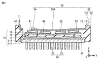
- FIG. 2 is a schematic cross-sectional view showing a modified example of the configuration of the power module according to the first embodiment.
- the power module 100 of the modified example of this embodiment has basically the same configuration as the power module 100 of FIG. Therefore, in FIG. 2, the same components as those in FIG. 1 are designated by the same reference numerals, and the description will not be repeated as long as the functions and the like are the same. This also applies to each of the following power modules unless otherwise specified.
- the main surface of the portion of the electrode plate 30 facing the insulating substrate 10 in the main body portion 30A follows a convex shape toward the heat radiating member 20 side of the insulating substrate 10.
- the main surface of the electrode plate 30 is warped so as to have a convex shape toward the heat radiating member 20 as in the insulating substrate 10.
- the electrode plate 30 is curved so that the lower surface has a convex shape when viewed from the outside and the upper surface has a concave shape when viewed from the outside.
- the electrode plate 30 of FIG. 2 is different from the electrode plate 30 of FIG. 1 in which the surface along the XY plane has almost no warp.
- FIG. 3 is a schematic cross-sectional view showing a second modification of the configuration of the power module according to the first embodiment.
- FIG. 4 is a schematic cross-sectional view showing a third modification of the configuration of the power module according to the first embodiment.
- the structure is basically the same as that of FIG. 1, but the conductor layer 12 on one surface 11A is formed thicker than the conductor layer 13 on the other surface 11B. It is different from 1.
- the conductor layer 12 on one surface 11A is formed thicker than the conductor layer 13 on the other surface 11B, although it has basically the same configuration as that in FIG. It differs from FIG. 2 in that it is.
- the insulating substrate 10 warps in a convex shape toward the heat radiating member 20.
- the insulating substrate 10 warps in a convex shape toward the heat radiating member 20. Further, for example, if the conductor layer 12 on one surface 11A is formed thicker than the conductor layer 13 on the other surface 11B, the insulating substrate 10 can be formed even if the first region and the second region have the same area. It warps in a convex shape toward the heat radiating member 20.
- FIG. 5 is a schematic cross-sectional view showing a fourth modification of the configuration of the power module according to the first embodiment.
- FIG. 6 is a schematic cross-sectional view showing a fifth modification of the configuration of the power module according to the first embodiment.
- it has basically the same configuration as that of FIG. 1, but another conductor layer 12a is arranged between the conductor layer 12 on one surface 11A and the IGBT 41 and the diode 42. ..
- the other conductor layer 12a is joined by a fourth solder 59a so as to overlap the conductor layer 12.
- FIG. 6 it has essentially the same configuration as FIG.
- FIGS. 5 and 6 are different from FIGS. 1 and 2 which do not have the other conductor layer 12a and the fourth solder 59a.
- the conductor layer on one surface 11A side of the base material 11 is substantially larger than the conductor layer 13 on the other surface 11B side. Functions as a thick one. Therefore, in FIGS. 5 and 6, similarly to FIGS. 3 and 4, the insulating substrate 10 warps in a convex shape toward the heat radiating member 20.
- FIGS. 7 to 10 show a method of manufacturing the power module 100 of FIG.
- FIG. 7 is a schematic cross-sectional view showing the first step of the method for manufacturing the power module according to FIG. 2 of the first embodiment.
- an insulating substrate 10 a heat radiating member 20, a semiconductor element, that is, an IGBT 41, a diode 42, and the like, a first solder 51, and a conductive material 59 are prepared.
- the insulating substrate 10 contains the base material 11.
- One or more conductor layers 12 are bonded on one surface 11A of the base material 11, and one or more conductor layers 13 are bonded on the other surface 11B on the opposite side of one surface 11A.
- the area difference between the first region and the second region is adjusted.
- the direction of warpage and the degree of curvature of the convex shape of the insulating substrate 10 after the members are joined by soldering are adjusted. Therefore, although the insulating substrate 10 is shown not to be curved in FIG. 7, it is actually slightly curved at this point.
- Each of the above members is positioned so as to have the configuration of the power module 100 of FIGS. 1 and 2. That is, a plate-shaped first solder 51 is arranged between the heat radiating member 20 and the conductor layer 13 of the insulating substrate 10. A plate-shaped conductive material 59 is arranged between the conductor layer 12 of the insulating substrate 10, the IGBT 41, and the diode 42. Each of these members is positioned so that it is placed at a position where it should be placed when it is joined to each other.
- FIG. 8 is a schematic cross-sectional view showing a second step of the power module manufacturing method according to FIG. 2 of the first embodiment.
- each of the above members is joined by the first solder 51 and the conductive material 59 by using a reflow device.
- all the above members are joined at the same time. That is, the heat radiating member 20 and the insulating substrate 10 are joined by the first solder 51.
- the IGBT 41 and the diode 42 are bonded to the insulating substrate 10.
- the conductor layers 12 and 13 of the insulating substrate 10 determine the bending direction and the amount of bending of the convex shape of the insulating substrate 10 after joining.
- the insulating substrate 10 is joined to the heat radiating member 20 so that the main surface warps so as to have a convex shape toward the heat radiating member 20. Since the insulating substrate 10 forms a convex shape, the first solder 51 is formed so as to be thicker at the end portion than at the center portion in a plan view.
- the heat radiating member 20 and the insulating substrate 10 may be joined by the first solder 51, and the insulating substrate 10 and the IGBT 41 may be joined by the conductive material 59 at the same time. However, these two joints may be made at different times rather than at the same time. However, in that case, it is preferable that the heat radiating member 20 and the insulating substrate 10 are first joined by the first solder 51, and then the insulating substrate 10 and the IGBT 41 or the like are joined by the conductive material 59.
- the heat generated when the insulating substrate 10 and the heat radiating member 20 are joined causes the heat.
- the conductive material 59 under the IGBT 41 may remelt. If it is remelted, the IGBT 41 or the like may be displaced with respect to the insulating substrate 10 due to the residual stress of the bonding wire (not shown) used for forming the circuit in the IGBT 41. From the viewpoint of preventing such a problem, it is preferable that the joining is performed in the above order.
- the following steps are performed after the step of joining the heat radiating member 20 and the insulating substrate 10 with the first solder 51 and the step of joining the IGBT 41 and the diode 42 to the insulating substrate 10 with the conductive material 59.
- NS The second solder 52 and the frame member 60 are prepared.
- the signal electrode 71 and the electrode plate 30 are partially embedded in the frame member 60.
- the signal electrode 71 is insert-molded so as to be partially exposed from the frame member 60.
- the second portion of the main terminal side end portion 33 which is a part of the main body portion 30A of the electrode plate 30, the bent portion, and the portion where the main body portion 30A is along the XY plane are the most in FIG. The area on the right is embedded.
- the electrode plate 30 is insert-molded so that these regions are embedded.
- the first portion 31 of the main terminal side end 33 as the main terminal 72 is exposed on the upper side of the frame member 60, and the portion of the electrode plate 30 along the XY plane and the semiconductor in the region surrounded by the frame member 60.
- the element side end 34 is exposed.
- a plate-shaped second solder 52 is arranged on the IGBT 41 and the diode 42. A portion of the electrode plate 30 along the XY plane is arranged on the second solder 52.
- the electrode plate 30 is curved by a generally known method in advance. Alternatively, the already curved electrode plate 30 may be purchased.
- the second solder 52, the electrode plate 30, and the frame member 60 are positioned so as to be arranged at positions where they should be arranged when they are joined to each other.
- FIG. 9 is a schematic cross-sectional view showing a third step of the power module manufacturing method according to FIG. 2 of the first embodiment.
- the frame member 60 in which the second portion 32 of the main terminal side end portion 33 is embedded is arranged so as to surround the insulating substrate 10 at intervals. It is heated using a reflow oven, and the electrode plate 30 is joined to the IGBT 41 and the diode 42 by the second solder 52. That is, the electrode plate 30 is joined to the IGBT 41 and the diode 42 by the second solder 52 so as to overlap at least a part of the IGBT 41 and the diode 42. More specifically, in this step, the main electrodes (not shown) of the IGBT 41 and the diode 42 are joined by the second solder 52 to the portion extending along the XY plane of the electrode plate 30.
- the base plate 21 of the heat radiating member 20 and the frame member 60 are joined by an adhesive (not shown).
- FIG. 10 is a schematic cross-sectional view showing a fourth step of the power module manufacturing method according to the first embodiment.
- the portion of the signal electrode 71 exposed inside the frame member 60 is electrically connected to the main electrode (not shown) of the IGBT 21 by the bonding wire 81.
- the liquid sealing material 90 is injected into the region surrounded by the frame member 60 and the heat radiating member 20. This is heated, for example, at 150 ° C. for 1.5 hours. As a result, the sealing material 90 is cured. As a result, each member surrounded by the frame member 60 is electrically insulated.
- FIG. 11 is a schematic cross-sectional view showing the first step of the method for manufacturing the power module according to FIG. 1 of the first embodiment.
- FIG. 12 is a schematic cross-sectional view showing a second step of the method for manufacturing the power module according to FIG. 1 of the first embodiment.
- FIG. 13 is a schematic cross-sectional view showing a third step of the method for manufacturing the power module according to FIG. 1 of the first embodiment.
- each member is prepared and positioned in the same manner as in FIG.
- FIG. 11 basically the same processing as in FIG. 8 is performed.
- the main body 30A of the electrode plate 30 has almost no warp.
- the thickness of the second solder 52 at the central portion is made larger than the thickness of the second solder 52 at the end portion.
- FIG. 12 basically the same processing as in FIG. 9 is performed.
- FIG. 13 basically the same processing as in FIG. 10 is performed.
- the conductor layer 12 on one surface 11A is formed thicker than the conductor layer 13 on the other surface 11B. May be done.
- another conductor layer 12a is formed between the conductor layer 12 and the IGBT 41 and the diode 42 on one surface 11A. May be joined so as to overlap the conductor layer 12. By doing so, the warp of the convex shape is adjusted so that the insulating substrate 10 warps toward the heat radiating member 20.
- in-vehicle power module there is a strong demand for compactness and weight reduction of in-vehicle power modules. Therefore, in an in-vehicle power module, it is necessary to arrange semiconductor elements capable of applying a high voltage and a large current at a high density. As a result, thermal interference between a plurality of arranged semiconductor elements may become a problem, and therefore, it is an important design requirement to be able to efficiently dissipate heat to the heat radiating member. Further, since the power module is mounted on a transportation device, high reliability is required from the viewpoint of stable transportation of passengers and the like.
- the base plate and fins that make up the heat dissipation member are often made of copper or aluminum, which has high thermal conductivity.
- copper and aluminum have a large difference in thermal expansion coefficient from aluminum nitride, which constitutes the base material of the insulating substrate, and silicon, which constitutes the semiconductor element. Since power modules for automobiles and electric railways generate a large amount of heat, it is necessary to join the heat radiating member and the insulating substrate with solder having better thermal conductivity than the heat radiating grease. Therefore, a large thermal stress is applied to the joint portion between the heat radiating member and the insulating substrate, and there is a possibility that the joint portion may be cracked in the evaluation of long-term reliability such as temperature cycle property.
- the insulating substrate may be unintentionally warped or tilted in the horizontal direction.
- wire bonding for circuit formation is performed on an insulating substrate or an IGBT having such an inclination
- the way the wire tool hits changes depending on the place where the wire bonding is to be performed. Therefore, it is necessary to readjust the way the wire tool hits each of the plurality of semiconductor elements, that is, each time the wire is bonded to different parts having different inclinations. If this adjustment is insufficient, the wire tool may damage the semiconductor element, making it difficult to wire-bond the wiring with high reliability.
- the power module 100 as the semiconductor device of the present embodiment includes an insulating substrate 10, a heat radiating member 20, and an electrode plate 30.
- the insulating substrate 10 mounts an IGBT 41 as a semiconductor element and a diode 42.
- the heat radiating member 20 is joined to the insulating substrate 10 by the first solder 51.
- the electrode plate 30 is arranged so as to overlap at least a part of the semiconductor element.
- the main surface of the insulating substrate 10 is curved so as to protrude toward the heat radiating member 20 and form a convex shape straddling a plurality of semiconductor elements.
- the first solder 51 is thicker at the edges than at the center in plan view.
- the semiconductor element is joined to the electrode plate 30 by the second solder 52.
- the heat radiating member 20 is joined to the insulating substrate 10 with, for example, a first solder 51 having better thermal conductivity than the heat radiating grease. Therefore, a large amount of heat generated by the semiconductor element is dissipated from the first solder 51 to the heat radiating member 20 with high efficiency.
- the main surface is warped so that the insulating substrate 10 has a convex shape toward the heat radiating member 20, and the first solder 51 becomes thicker at the end than at the center.
- the first solder 51 has a large thermal strain at the end in a plan view, but the convex shape makes the first solder 51 at the end thicker, so that the thermal strain at the end can be reduced. Therefore, long-term reliability such as temperature cycleability can be improved, and for example, the occurrence of cracks in the first solder 51 can be suppressed.
- the thermal resistance is reduced by thinning the first solder 51 in the central portion where the temperature is highest due to thermal interference. Therefore, heat can be radiated from the first solder 51 to the heat radiating member 20 with high efficiency.
- the semiconductor element is joined to the electrode plate 30 by the second solder 52. Therefore, for example, when the power module 100 is electrically connected to the outside by wire bonding directly to the semiconductor element, the contact of the insulating substrate 10 and the wire tool based on the inclination angle of the semiconductor element from the horizontal direction can occur. There is no need to make adjustments. Therefore, damage to the semiconductor element of the wire tool due to the adjustment of the contact method of the wire tool can be suppressed. Therefore, the reliability of the electrical connection between the semiconductor element inclined in the horizontal direction due to the warp of the insulating substrate 10 and the outside of the power module 100 is higher than that in the case where the electrical connection is made by the bonding wire. Can be enhanced.
- the insulating substrate 10 includes the base material 11.
- One or more conductor layers 12 and 13 are bonded onto one surface 11A of the base material 11 and on the other surface 11B opposite to one surface 11A.
- the first solder 51 joins the entire surface of the conductor layer 13 on the other surface 11B.
- the first solder 51 gradually becomes thicker from the central portion to the end portion in a plan view. Such a configuration may be used, and the same effect as described above can be obtained.
- the power module 100 further includes a frame member 60 arranged so as to surround the insulating substrate 10 at intervals from the insulating substrate 10.
- the semiconductor element and the electrode plate 30 are joined by the second solder 52. Therefore, unlike bonding at room temperature by wire bonding, for example, the second solder 52 is heated and melted at the time of bonding. With this heating, the insulating substrate 10 may be warped unintentionally. As a result, the insulating substrate 10 deformed more than expected interferes with the frame member 60, so that stress is generated in the insulating substrate 10 and there is a concern that the corners thereof may be chipped or cracked.
- the frame member 60 is arranged at intervals from the insulating substrate 10 and the semiconductor element as described above.
- a sealing material 90 made of a silica filler-containing epoxy resin or the like.
- the large difference in the coefficient of thermal expansion between the base material 11 of the insulating substrate 10 and the heat radiating member 20 is large, and cracks may occur in the first solder 51 when evaluating the temperature cycle property of the first solder 51. ..
- the sealing material 90 between the two, the difference in the coefficient of thermal expansion between the base material 11 and the sealing material 90 and between the heat radiating member 20 and the sealing material 90 can be made smaller than the above. .. Therefore, the possibility of cracks occurring in the first solder 51 during long-term reliability evaluation such as the temperature cycle property of the first solder can be reduced, and the reliability of the power module 100 can be improved.
- the electrode plate 30 is arranged in the frame member 60 so as to face the insulating substrate 10.
- the main surface of the electrode plate 30 may be warped so as to follow the convex shape of the insulating substrate 10.
- the thickness of the second solder 52 that joins the electrode plate 30 and the semiconductor element becomes constant among the plurality of semiconductor elements. Therefore, the electrode plate 30 and the semiconductor element can be reliably and stably joined by the second solder 52.
- the semiconductor element includes a diode 42 as a first semiconductor element and an IGBT 41 as a second semiconductor element arranged in a region closer to a frame member in a plan view than the first semiconductor element.
- the maximum thickness of the second solder 52 between the electrode plate 30 and the first semiconductor element may be thicker than the maximum thickness of the second solder 52 between the electrode plate 30 and the second semiconductor element. ..
- this mode is adopted.
- the second solder 52 that comes into contact with the second semiconductor element is the second solder 52 that comes into contact with the first semiconductor element. Becomes thinner than. By doing so, the total thermal resistance from the semiconductor element to the heat radiating member 20 can be made smaller.
- the electrode plate 30 includes a main terminal side end 33 as a main terminal 72 and a semiconductor element side end 34 which is an end opposite to the main terminal side end.
- the main terminal side end portion 33 has a first portion 31 exposed to the outside of the frame member 60 and a second portion 32 embedded in the frame member.
- the electrode plate 30 is electrically connected to the main terminal 72 as an integral body. Therefore, the electrical connection structure between the semiconductor element and the outside of the power module 100 can be further simplified.
- the power module 100 further includes a sealing material 90 as a sealing resin for sealing the semiconductor element.
- the first solder 51 is in contact with the sealing material 90.
- a sealing material 90 made of a silica filler-containing epoxy resin or the like.
- the large difference in the coefficient of thermal expansion between the base material 11 of the insulating substrate 10 and the heat radiating member 20 is large, and cracks may occur in the first solder 51 when evaluating the temperature cycle property of the first solder 51. ..
- the sealing material 90 between the two, the difference in the coefficient of thermal expansion between the base material 11 and the sealing material 90 and between the heat radiating member 20 and the sealing material 90 can be made smaller than the above. .. Therefore, the possibility of cracks occurring in the first solder 51 during long-term reliability evaluation such as the temperature cycle property of the first solder can be reduced, and the reliability of the power module 100 can be improved.
- the heat radiating member 20 and the insulating substrate 10 are joined by the first solder 51.
- the IGBT 41 as a semiconductor element and the diode 42 are bonded to the insulating substrate 10.
- the electrode plate 30 that overlaps at least a part of the semiconductor element is joined to the semiconductor element by the second solder 52.
- the insulating substrate 10 is joined to the heat radiating member 20 so that the main surface warps so as to have a convex shape toward the heat radiating member 20.
- the first solder 51 is formed so as to be thicker at the end portion than at the center portion in a plan view. Since the action and effect by this are the same as the action and effect by the basic configuration of the power module 100 described above, the description thereof will not be repeated.
- the insulating substrate 10 includes the base material 11.
- One or more conductor layers 12 and 13 are bonded onto one surface 11A of the base material 11 and on the other surface 11B opposite to one surface 11A.
- the convex warp is adjusted by adjusting the area difference between the first region on one surface 11A where the conductor layer 12 is not joined and the second region on the other surface 11B where the conductor layer 13 is not joined. In this way, the direction and amount of warpage of the main surface of the insulating substrate 10 can be controlled.
- the convex warp may be adjusted by forming the conductor layer 12 on one surface 11A thicker than the conductor layer 13 on the other surface 11B.
- the insulating substrate 10 can be adjusted so as to warp toward the heat radiating member 20 in a convex shape.
- the step of joining the conductor layer 12 on one surface 11A and the other conductor layer 12a between the IGBT 41 and the diode 42 so as to overlap the conductor layer 12 is further provided.
- the warp of the convex shape may be adjusted.
- the insulating substrate 10 can be adjusted so as to warp toward the heat radiating member 20 in a convex shape.
- FIG. 14 is a schematic cross-sectional view showing the configuration of the power module according to the second embodiment.
- the base plate 21 of the heat radiating member 20 includes the first heat radiating member portion 21A and the second heat radiating member portion 21B.
- the first heat radiating member portion 21A is a plate-shaped portion having a surface along the XY plane, similarly to the base plate 21 of the first embodiment. Therefore, the uppermost surface of the first heat radiating member portion 21A in the Z direction is joined to the lower main surface of the insulating substrate 10 by the first solder 51.
- the second heat radiating member portion 21B is arranged outside the first heat radiating member portion 21A in a plan view so as to be integrated with the first heat radiating member portion 21A.
- the second heat radiating member portion 21B is arranged so as to surround the first heat radiating member portion 21A and the first solder 51 on the first heat radiating member portion 21A in a plan view.
- the second heat radiating member portion 21B is arranged at a position where the coordinates in the Z direction are the same as those of the first heat radiating member portion 21A, and in a region extending upward in the Z direction from the position. Therefore, the second heat radiating member portion 21B is formed thick so as to extend upward (insulated substrate 10 side) in the Z direction from the first heat radiating member portion 21A.
- the frame member 60 is mounted on the second heat radiating member portion 21B formed to be thicker than the first heat radiating member portion 21A.
- a recess is formed by the first heat radiating member portion 21A and the second heat radiating member portion 21B integrally formed on the outside of the first heat radiating member portion 21A.
- This recess accommodates the first solder 51 and the insulating substrate 10.
- the base plate 21 of FIG. 14 is different from the base plate 21 of FIG. 1 which has only a flat plate member portion and does not form a recess as shown in FIG.
- This embodiment exhibits the following effects in addition to the same effects as those of the basic configuration of the first embodiment. This also applies to each of the following embodiments unless otherwise specified.
- the power module 100 of the present embodiment includes a first heat radiating member portion 21A and a second heat radiating member portion 21B.
- the first heat radiating member portion 21A is joined to the insulating substrate 10 by the first solder 51.
- the second heat radiating member portion 21B surrounds the first heat radiating member portion 21A and the first solder 51 on the outside of the first heat radiating member portion 21A in a plan view, and mounts the frame member 60.
- a recess formed by the first heat radiating member portion 21A and the second heat radiating member portion 21B accommodates the first solder 51 and the insulating substrate 10.
- the first solder 51 can be made thinner and its rigidity can be lowered without lowering the rigidity of the entire base plate 21 as compared with the first embodiment. Therefore, it is possible to suppress the occurrence of cracks in the first solder 51 in the evaluation of long-term reliability such as temperature cycleability. Further, the thickness of the frame member 60 on the second heat radiating member portion 21B is reduced by the amount of the arrangement.
- the PPS resin constituting the frame member 60 has poor adhesion to the sealing material 90. Therefore, by reducing the dimension of the frame member 60 in the Z direction, the area of the adhesive interface between the sealing material 90 and the frame member 60 can be reduced, and peeling between the two can be suppressed.
- FIG. 15 is a schematic cross-sectional view showing the configuration of the power module according to the third embodiment.
- the electrode plate 30 does not have a region corresponding to the main terminal 72, and the frame member 60 on the right side of the figure is further provided with the main terminal 73.
- the main terminal 73 corresponds to the main terminal 72 of the first embodiment.
- the main terminal 73 is integrated with the electrode plate 30, that is, is not a part of the main body 30A of the electrode plate 30.
- the main terminal 73 is a member different from the electrode plate 30.
- the main terminal 73 includes a first portion 73A, a second portion 73B, and a third portion 73C.
- the first portion 73A is a portion corresponding to the first portion 31 of the main terminal 72 of FIG.
- the first portion 73A is a portion exposed to the outside of the frame member 60 so as to extend along the Z direction.
- the second portion 73B is a portion corresponding to the second portion 32 of the main terminal 72 of FIG.
- the second portion 73B is a portion embedded in the frame member 60, and includes a portion in which the main terminal 73 bends in FIG.
- the third portion 73C is a portion as a connecting portion in which the main terminal 73 is connected to the main terminal side end portion 33 of the electrode plate 30 inside the frame member 60.
- the third portion 73C which is a connecting portion, is exposed from the frame member 60 inside the frame member 60, but is buried in the sealing material 90. Even if it is buried in the sealing material 90 in the final product, it is exposed from at least the frame member 60. Therefore, in the present specification, such a third portion 73C is expressed as "exposed from the frame member 60". There is.
- the main terminal 73 is arranged as a separate member independent of the electrode plate 30. Therefore, the main body portion 30B of the electrode plate 30 does not have a main terminal, but has only a portion extending in the horizontal direction along the XY plane.
- the main body portion 30B of the electrode plate 30 of FIG. 15 includes a main terminal side end portion 33 and a semiconductor element side end portion 34.
- the main terminal side end portion 33 is the rightmost region in the X direction of the main body portion 30B in FIG.
- the main terminal side end 33 is connected to the main terminal 73.
- the semiconductor element side end portion 34 is a region opposite to the main terminal side end portion 33, that is, the leftmost end portion of the main body portion 30B in FIG. 15 in the X direction.
- the main terminal side end 33 of the electrode plate 30 and the third portion 73C, which is the connecting portion of the main terminal 73, are joined by the third solder 53. That is, the portion where the main terminal side end portion 33 faces downward in the Z direction and the portion of the third portion 73C facing upward in the Z direction are joined by the third solder 53. Therefore, it is preferable that the rightmost region in the X direction of FIG. 15 extends to a position where the rightmost region of the main terminal side end portion 33 overlaps with the third portion 73C of the main terminal 73 in a plan view.
- the material of the main body 30B of the electrode plate 30 and the main terminal 73 of the present embodiment is a metal material such as copper similar to the material of the main body 30A of the electrode plate 30 and the signal electrode 71 in the first embodiment. ..
- the signal electrode 71, the main terminal 73, and the main body 30B of the electrode plate 30 may be a single lead frame divided into three parts.
- the main body 30B is preferably formed of a metal material such as copper.
- the electrode plate 30 and the main terminal 73 are separate members, and both are electrically connected by a third solder 53.
- the present embodiment is structurally different from the first and second embodiments in which the electrode plate 30 is integrated with the main terminal and these are directly connected.
- the manufacturing method of the power module 100 shown in FIG. 15 will be described with reference to FIGS. 16 to 19.
- the description will be given here using an example in which the electrode plate 30 is not curved in advance and the main surface has a planar shape, the electrode plate 30 is curved in advance in the present embodiment as in FIGS. 7 to 10. May be used. This also applies to each of the following embodiments.
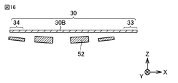
- FIG. 16 is a schematic cross-sectional view showing the first step of the power module manufacturing method according to the third embodiment.
- first the same processing as in FIG. 7 is performed, and each member in FIG. 7 is joined by the first solder 51 and the conductive material 59 by the reflow device.
- the second solder 52 and the electrode plate 30 are prepared. This corresponds to the step in which the second solder 52 and the frame member 60 are prepared after the joining step in FIG.
- an electrode plate 30 made of a flat plate-shaped main body portion 30B having no main terminal and therefore having no bent portion is prepared. Further, it is assumed that the thickness of the second solder 52 is larger at the central portion than at the end portion from the viewpoint of joining the flat plate-shaped electrode plate 30 and the semiconductor element.
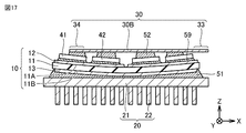
- FIG. 17 is a schematic cross-sectional view showing a second step of the power module manufacturing method according to the third embodiment.
- the electrode plate 30 is joined to the IGBT 41 and the diode 42 by the second solder 52 so as to overlap at least a part on the IGBT 41 and the diode 42, as in the process of FIG. ..
- FIG. 18 is a schematic cross-sectional view showing a third step of the power module manufacturing method according to the third embodiment.
- the frame member 60 is prepared.
- the signal electrode 71 is insert-molded so as to be partially exposed from the frame member 60.
- the main terminal 73 is embedded by insert molding so as to be partially exposed from the frame member 60.
- FIG. 19 is a schematic cross-sectional view showing a fourth step of the power module manufacturing method according to the third embodiment.
- heating is performed using a reflow furnace, and the electrode plate 30 and the third portion 73C of the main terminal 73 are joined by the third solder 53.
- the power module 100 of FIG. 15 is formed by joining the base plate 21 and the frame member 60 with the adhesive shown in FIG. 9 and performing the same processing as in FIG.
- the power module 100 of this embodiment further includes a main terminal 73.
- the main terminal 73 includes a third portion 73C as a connecting portion exposed from the frame member 60 inside the frame member 60.
- the electrode plate 30 includes a main terminal side end 33 connected to the main terminal 73, and a semiconductor element side end 34 which is an end opposite to the main terminal side end 33.
- the main terminal side end 33 of the electrode plate 30 and the third portion 73C are joined by a third solder 53.
- a frame member 60 is prepared which is arranged so as to surround the insulating substrate 10 at intervals from the insulating substrate 10 and in which the main terminal 73 is embedded. After the step of joining the electrode plate 30 to the semiconductor element with the second solder 52, the electrode plate 30 and the main terminal 73 are joined with the third solder 53.
- the difference between the thickness of the second solder 52 at the center in the plan view and the thickness of the second solder 52 at the end in the plan view may become large.
- problems such as partial tearing of the second solder 52 can be suppressed.
- the main terminal 73 and the electrode plate 30 are joined by the third solder 53. Therefore, by adjusting the supply amount of the third solder 53 and the like, the stress applied to the second solder 52 due to the deformation of the electrode plate 30 can be absorbed at the joint portion of the third solder 53.
- FIG. 20 is a schematic cross-sectional view showing the configuration of the power module according to the fourth embodiment.
- the power module 100 of the present embodiment has basically the same configuration as the power module 100 of FIG. 15 of the third embodiment.
- the main body 30C of the electrode plate 30 does not have a main terminal and has only a portion extending in the horizontal direction along the XY plane. Therefore, in FIG. 20, the same components as those in FIG. 15 are designated by the same reference numerals, and the description will not be repeated as long as the functions and the like are the same.
- FIG. 20 the same components as those in FIG. 15 are designated by the same reference numerals, and the description will not be repeated as long as the functions and the like are the same.
- FIG. 20 the same components as those in FIG. 15 are designated by the same reference numerals, and the description will not be repeated as long as the functions and the like are the same.
- FIG. 20 the same components as those in FIG. 15 are designated by the same reference numerals, and the description will not be repeated as
- the main terminal side end 33 of the electrode plate 30 and the third portion 73C, which is the connecting portion of the main terminal 73, are bonded by the bonding wire 82.
- the bonding wire 82 extends in the direction along the X direction. Therefore, in the main body portion 30C of the electrode plate 30, the rightmost region of the main terminal side end portion 33 in the X direction is connected to the electrode plate 30 by exposing the main terminal 73 from the frame member 60 as shown in FIG. It does not have to extend to a position where it overlaps with the three portions 73C in a plan view. In FIG. 20, the main terminal side end 33 extends to a region that overlaps with the IGBT 41 on the right side of FIG. 20 in a plan view, and does not extend further to the right.
- the material and dimensions of the bonding wire 82 are preferably the same as those of the bonding wire 81.
- the material of the main body 30C is preferably a metal material such as copper as in the main bodies 30A and 30B.
- the electrode plate 30 and the main terminal 73 are separate members, and both are electrically connected by a bonding wire 82.
- the present embodiment is structurally different from the first and second embodiments in which the electrode plate 30 is integrated with the main terminal and these are directly connected.
- FIG. 21 is a schematic cross-sectional view showing the first step of the method for manufacturing the power module according to the fourth embodiment.
- first the same processing as in FIGS. 16 to 18 of the third embodiment is performed.
- the rightmost region in the X direction of the main terminal side end 33 on the main terminal 73 side of the flat plate-shaped main body 30C may be arranged on the left side of the third embodiment.
- FIG. 22 is a schematic cross-sectional view showing a second step of the power module manufacturing method according to the fourth embodiment.
- the electrode plate 30 and the third portion 73C of the main terminal 73 are bonded by a wire bonding step, that is, by a bonding wire 82.
- Subsequent steps are the same as in the third embodiment.
- the power module 100 of FIG. 20 is formed.
- the power module 100 of this embodiment further includes a main terminal 73.
- the main terminal 73 includes a third portion 73C as a connecting portion exposed from the frame member inside the frame member 60.
- the electrode plate 30 includes a main terminal side end 33 connected to the main terminal 73, and a semiconductor element side end 34 which is an end opposite to the main terminal side end 33.
- the main terminal side end 33 of the electrode plate 30 and the third portion 73C are bonded by a bonding wire 82.
- a frame member 60 is prepared which is arranged so as to surround the insulating substrate 10 at intervals from the insulating substrate 10 and in which the main terminal 73 is embedded. After the step of joining the electrode plate 30 to the semiconductor element with the second solder 52, the electrode plate 30 and the main terminal 73 are joined by a wire bonding step.
- the wire tool damages the semiconductor element. Problems such as giving can occur.
- the electrode plate 30 is bonded to the main terminal 73 by wire bonding via the electrode plate 30 between the semiconductor element and the main terminal 73.
- the number of bonding wires 81 and 82 can be reduced as compared with the case of wire bonding directly on the semiconductor element.
- the possibility that the wire tool damages the semiconductor element due to the inclination of the surface of the semiconductor element due to the warp of the insulating substrate 10 can be reduced, and the reliability of the bonding wires 81 and 82 can be improved.
- FIG. 23 is a schematic cross-sectional view showing the configuration of the power module according to the fifth embodiment.
- the protrusion 21C is formed on the heat radiating member 20.
- the base plate 21 of the heat radiating member 20 has a protrusion having an apex at a position where it overlaps with the region where the temperature is highest on the other surface 11B side, which is the back surface of the insulating substrate 10 during operation of the semiconductor element, and in a plan view.
- Part 21C is formed.
- FIG. 23 shows an example in which the temperature is highest during the operation of the semiconductor element in the central portion of the insulating substrate 10 in a plan view.
- a protrusion 21C having an apex is formed at a position of the base plate 21 that overlaps the central portion of the insulating substrate 10 in a plan view.
- it is the semiconductor element that reaches the maximum temperature during operation, but when viewed from the back surface of the insulating substrate 10, heat is diffused and the peak of the heat distribution is blurred, so that the temperature is highest in the central portion.
- the protrusion 21C is formed on the uppermost surface where the base plate 21 comes into contact with the first solder 51.
- the protrusion 21C has a convex shape with the uppermost surface bulging upward so that the uppermost surface of the base plate 21 is arranged at the uppermost position at the apex. Therefore, the base plate 21 has the largest thickness in the protrusion 21C.
- the apex of the protrusion 21C is preferably thicker by about 0.1 mm than the thinnest end of the base plate 21.
- the first solder 51 in the region where the temperature becomes high can be made thinner, and the first solder 51 at the end can be made thicker. Therefore, the thermal resistance of the first solder 51 in the central region where the temperature is high is reduced, so that the heat dissipation is improved. Further, the thermal strain in the first solder 51 can be reduced at the end portion, and the occurrence of cracks in the first solder 51 can be suppressed.
- FIG. 24 is a schematic cross-sectional view showing the configuration of the power module according to the sixth embodiment.
- the insulating substrate 10 includes a curved portion 10A and a non-curved portion 10B.
- the curved portion 10A is a portion whose main surface is curved so that the insulating substrate 10 has a convex shape toward the heat radiating member 20 side, as in the other embodiment.
- the non-curved portion 10B is a region in which the insulating substrate 10 is not warped like the curved portion 10A, and the main surface spreads flatly along the XY plane.
- the curved portion 10A and the non-curved portion 10B are arranged so as to be aligned in the horizontal direction.
- the first solder 51 is the thinnest at a position overlapping the central portion of the curved portion 10A.
- the first solder 51 is the thinnest at a position overlapping the central portion in the plan view of the entire insulating substrate 10 in which the curved portion 10A and the non-curved portion 10B are combined.
- the first solder 51 may be thick at the end.
- the IGBT 41 and the diode 42 are mounted on the conductor layer 12 in the curved portion 10A as in other embodiments.
- the control semiconductor element 43 is mounted on the conductor layer 12 in the non-curved portion 10B.
- the control semiconductor element 43 is usually an IC (Integrated Circuit) in which a program for driving an IGBT 41, a diode 42, or the like is written, that is, a so-called microcomputer or the like.
- the conductor layer 12 is shown so as to be continuous from the curved portion 10A to the non-curved portion 10B. However, the conductor layer 12 may be divided between the curved portion 10A and the non-curved portion 10B so as to be separate members.
- the power module 100 may have such a configuration.
- the control semiconductor element 43 hardly generates heat. Therefore, the first solder 51 at the position where it overlaps with the control semiconductor element 43 may be formed as thick as the end portion of the first solder 51 as a whole. That is, the thickness of the first solder 51 may be substantially the same in the entire non-curved portion 10B. In this way, the surface of the control semiconductor element 43 in the non-curved portion 10B is arranged along the horizontal direction, that is, so as to have almost no inclination. Therefore, the control semiconductor element 43 can reduce the possibility of damaging the control semiconductor element due to the inclination when wire bonding on the control semiconductor element 43.
- FIG. 25 is a schematic cross-sectional view showing the configuration of the power module according to the seventh embodiment.
- the power module 100 may be configured without the frame member 60.
- the sealing material 91 of the power module 100 seals each of the other members so as to expose at least a part of the lowermost surface of the base plate 21 and the entire fin 22. Since the frame member 60 is not provided, the sealing material 91 forms the outermost surface of the power module 100.
- the main body 30D of the electrode plate 30 is arranged as a separate member independent of each of the main terminal 73 and the signal electrode 71.
- the main body portion 30D has only a portion that extends in the horizontal direction along the XY plane.
- the signal electrode 71 and the main terminal 73 may be arranged so as to be arranged on the same plane so that the main body portion 30D is aligned with the same plane as the XY plane on which the main body portion 30D extends. ..
- the main body 30D and the signal electrode 71 are connected by a bonding wire 81 as in other embodiments.
- the main body 30D and the main terminal 73 may be connected by any means such as any of the third solder 53 and the bonding wire 82.
- the signal electrode 71, the main terminal 73, and the main body 30D of the electrode plate 30 may be a single lead frame divided into three parts.
- the main body portion 30D and the main terminal 73 may be integrated. Therefore, the main body 30D is preferably formed of a metal material such as copper.
- the sealing material 91 is preferably an epoxy resin containing a silica filler, which is formed by a transfer molding method. Specifically, in the transfer molding process, for example, the following processing is performed. Each member such as the base plate 21, the insulating substrate 10, and the semiconductor element of FIG. 25 is laminated so as to include at least a part of the main body portion 30D and the signal electrode 71 in the mold, and is fixed so as to be sandwiched. NS. At this time, the mold is heated to 170 ° C. The mold is a machined product of stainless steel. Next, a solid resin tablet for transfer molding is poured into the mold while being heated and pressurized. The resin is cured by heating the entire inside of the mold at 170 ° C. for 1 minute.
- the whole including the sealing material 91 as the cured resin is removed from the mold.
- the whole removed from the mold is heated in the oven at 170 ° C. for 2 hours.
- the power module 100 having the aspect of the sealing material 91 of FIG. 25 is formed. Since the action and effect of the present embodiment are the same as the action and effect of the first embodiment, the description thereof will not be repeated.
- the first sample has a configuration similar to that of the power module 100 shown in FIG. That is, in the first sample, the main surface of the insulating substrate 10 is warped so as to have a convex shape toward the heat radiating member 20 side.
- the thickness of the first solder 51 in FIG. 1 is 0.2 mm at the central portion and 0.4 mm at the end portion. That is, the thickness of the first solder 51 is larger at the end than at the center, as in the first embodiment.
- the second sample has basically the same structure as the first sample, but the thickness of the first solder 51 is the same at the center and the ends. In the second sample, the thickness of the first solder 51 is 0.3 mm at both the central portion and the end portion.
- the third sample has basically the same structure as the first sample, but the thickness of the first solder 51 is 0.3 mm at the central portion and 0.2 mm at the end portion. That is, the thickness of the first solder 51 is smaller at the end than at the center, contrary to the first embodiment.
- FIG. 26 is a graph showing the result of measuring the maximum length of the crack formed at the end of the first solder.
- the horizontal axis of FIG. 26 indicates the number of times the above one cycle was repeated for each sample.
- the vertical axis of FIG. 26 shows the maximum length of cracks at the end of the first solder 51 after the above one cycle is repeated a plurality of times.
- the black circle in FIG. 26 indicates the first sample.
- the white triangle in FIG. 26 indicates the second sample.
- the white square in FIG. 26 shows the third sample.
- the first sample hardly developed cracks even after being repeated for 1000 cycles.
- the second sample after repeating 1000 cycles, cracks developed by about 10 mm from the end of the first solder 51.
- After 1000 cycles of the third sample cracks developed by about 22 mm from the end of the first solder 51.
- FIG. 27 is an ultrasonic flaw detection image of the end of the first solder after the temperature cycle test of the first sample.
- FIG. 28 is an ultrasonic flaw detection image of the end of the first solder after the temperature cycle test of the third sample.
- the cracks of the first solder 51 were hardly extended before and after the temperature cycle test and after 1000 cycles.
- the third sample cracks hardly extended to the first solder 51 before the temperature cycle test, whereas cracks having a length L in the figure were found after 1000 cycles. It was formed. From the above, it was confirmed that cracks can be suppressed by making the first solder thicker at the edges than at the center in a plan view.
- each of the above-described embodiments may be applied so as to be appropriately combined within a technically consistent range.
- the configuration having the main body portions 30B and 30C and the main terminal 73 may be applied as in the third and fourth embodiments.
Landscapes
- Cooling Or The Like Of Semiconductors Or Solid State Devices (AREA)
- Structures Or Materials For Encapsulating Or Coating Semiconductor Devices Or Solid State Devices (AREA)
- Chemical & Material Sciences (AREA)
- Engineering & Computer Science (AREA)
- Ceramic Engineering (AREA)
Priority Applications (3)
| Application Number | Priority Date | Filing Date | Title |
|---|---|---|---|
| CN202180022576.6A CN115315805B (zh) | 2020-03-26 | 2021-03-25 | 半导体装置及其制造方法 |
| JP2022510662A JP7233604B2 (ja) | 2020-03-26 | 2021-03-25 | 半導体装置およびその製造方法 |
| US17/798,100 US20230118890A1 (en) | 2020-03-26 | 2021-03-25 | Semiconductor device, and manufacturing method therefor |
Applications Claiming Priority (2)
| Application Number | Priority Date | Filing Date | Title |
|---|---|---|---|
| JP2020-056429 | 2020-03-26 | ||
| JP2020056429 | 2020-03-26 |
Publications (1)
| Publication Number | Publication Date |
|---|---|
| WO2021193823A1 true WO2021193823A1 (ja) | 2021-09-30 |
Family
ID=77890481
Family Applications (1)
| Application Number | Title | Priority Date | Filing Date |
|---|---|---|---|
| PCT/JP2021/012535 Ceased WO2021193823A1 (ja) | 2020-03-26 | 2021-03-25 | 半導体装置およびその製造方法 |
Country Status (4)
| Country | Link |
|---|---|
| US (1) | US20230118890A1 (https=) |
| JP (1) | JP7233604B2 (https=) |
| CN (1) | CN115315805B (https=) |
| WO (1) | WO2021193823A1 (https=) |
Cited By (1)
| Publication number | Priority date | Publication date | Assignee | Title |
|---|---|---|---|---|
| CN115070157A (zh) * | 2022-05-27 | 2022-09-20 | 北京萃锦科技有限公司 | 一种有利于改善热阻的底板结构 |
Families Citing this family (3)
| Publication number | Priority date | Publication date | Assignee | Title |
|---|---|---|---|---|
| TW202326927A (zh) | 2021-10-15 | 2023-07-01 | 日商東京威力科創股份有限公司 | 基板處理裝置 |
| CN114334920A (zh) * | 2021-12-31 | 2022-04-12 | 佛山市国星光电股份有限公司 | 分立器件、功率模块和散热系统 |
| WO2024247052A1 (ja) * | 2023-05-29 | 2024-12-05 | 三菱電機株式会社 | 電力変換装置およびその製造方法 |
Citations (8)
| Publication number | Priority date | Publication date | Assignee | Title |
|---|---|---|---|---|
| JPH10154774A (ja) * | 1996-11-26 | 1998-06-09 | Hitachi Ltd | 半導体モジュール |
| JP2000200865A (ja) * | 1999-01-06 | 2000-07-18 | Shibafu Engineering Kk | 絶縁基板及び半導体装置 |
| JP2003209199A (ja) * | 2002-01-15 | 2003-07-25 | Kyocera Corp | 半導体素子搭載用基板 |
| JP2012160548A (ja) * | 2011-01-31 | 2012-08-23 | Toyota Central R&D Labs Inc | 絶縁基板とその絶縁基板を有するパワーモジュール |
| JP2014011236A (ja) * | 2012-06-28 | 2014-01-20 | Honda Motor Co Ltd | 半導体装置、並びに、半導体装置の製造装置及び製造方法 |
| JP2016058563A (ja) * | 2014-09-10 | 2016-04-21 | 三菱電機株式会社 | 半導体装置およびその製造方法 |
| JP2016115900A (ja) * | 2014-12-18 | 2016-06-23 | 三菱電機株式会社 | 半導体モジュールおよび半導体装置 |
| WO2018146933A1 (ja) * | 2017-02-13 | 2018-08-16 | 富士電機株式会社 | 半導体装置及び半導体装置の製造方法 |
Family Cites Families (11)
| Publication number | Priority date | Publication date | Assignee | Title |
|---|---|---|---|---|
| JP2005347684A (ja) * | 2004-06-07 | 2005-12-15 | Nissan Motor Co Ltd | 半導体装置 |
| TWI246756B (en) * | 2004-06-28 | 2006-01-01 | Siliconware Precision Industries Co Ltd | Semiconductor package having exposed heat sink and heat sink therein |
| JP4777681B2 (ja) * | 2005-04-08 | 2011-09-21 | Okiセミコンダクタ株式会社 | 陽極接合装置、陽極接合方法及び加速度センサの製造方法 |
| JP2007258435A (ja) * | 2006-03-23 | 2007-10-04 | Mitsubishi Electric Corp | 半導体装置 |
| JP6124810B2 (ja) * | 2014-01-16 | 2017-05-10 | 三菱電機株式会社 | パワーモジュール |
| US10636723B2 (en) * | 2014-08-06 | 2020-04-28 | Denka Company Limited | Heat dissipation component and method for manufacturing same |
| JP6498566B2 (ja) * | 2015-08-24 | 2019-04-10 | 京セラ株式会社 | パワー半導体モジュール及びその製造方法 |
| JP6462529B2 (ja) * | 2015-08-24 | 2019-01-30 | 京セラ株式会社 | パワー半導体モジュールの製造方法及びパワー半導体モジュール |
| CN110574159B (zh) * | 2017-05-11 | 2023-04-04 | 三菱电机株式会社 | 功率模块、电力变换装置以及功率模块的制造方法 |
| JP7047900B2 (ja) * | 2018-04-06 | 2022-04-05 | 三菱電機株式会社 | 半導体装置および電力変換装置ならびに半導体装置の製造方法 |
| JP2019054296A (ja) * | 2019-01-10 | 2019-04-04 | 京セラ株式会社 | パワー半導体モジュール |
-
2021
- 2021-03-25 JP JP2022510662A patent/JP7233604B2/ja active Active
- 2021-03-25 WO PCT/JP2021/012535 patent/WO2021193823A1/ja not_active Ceased
- 2021-03-25 US US17/798,100 patent/US20230118890A1/en active Pending
- 2021-03-25 CN CN202180022576.6A patent/CN115315805B/zh active Active
Patent Citations (8)
| Publication number | Priority date | Publication date | Assignee | Title |
|---|---|---|---|---|
| JPH10154774A (ja) * | 1996-11-26 | 1998-06-09 | Hitachi Ltd | 半導体モジュール |
| JP2000200865A (ja) * | 1999-01-06 | 2000-07-18 | Shibafu Engineering Kk | 絶縁基板及び半導体装置 |
| JP2003209199A (ja) * | 2002-01-15 | 2003-07-25 | Kyocera Corp | 半導体素子搭載用基板 |
| JP2012160548A (ja) * | 2011-01-31 | 2012-08-23 | Toyota Central R&D Labs Inc | 絶縁基板とその絶縁基板を有するパワーモジュール |
| JP2014011236A (ja) * | 2012-06-28 | 2014-01-20 | Honda Motor Co Ltd | 半導体装置、並びに、半導体装置の製造装置及び製造方法 |
| JP2016058563A (ja) * | 2014-09-10 | 2016-04-21 | 三菱電機株式会社 | 半導体装置およびその製造方法 |
| JP2016115900A (ja) * | 2014-12-18 | 2016-06-23 | 三菱電機株式会社 | 半導体モジュールおよび半導体装置 |
| WO2018146933A1 (ja) * | 2017-02-13 | 2018-08-16 | 富士電機株式会社 | 半導体装置及び半導体装置の製造方法 |
Cited By (2)
| Publication number | Priority date | Publication date | Assignee | Title |
|---|---|---|---|---|
| CN115070157A (zh) * | 2022-05-27 | 2022-09-20 | 北京萃锦科技有限公司 | 一种有利于改善热阻的底板结构 |
| CN115070157B (zh) * | 2022-05-27 | 2024-06-04 | 浙江萃锦半导体有限公司 | 一种有利于改善热阻的底板结构 |
Also Published As
| Publication number | Publication date |
|---|---|
| CN115315805B (zh) | 2025-01-10 |
| CN115315805A (zh) | 2022-11-08 |
| JP7233604B2 (ja) | 2023-03-06 |
| JPWO2021193823A1 (https=) | 2021-09-30 |
| US20230118890A1 (en) | 2023-04-20 |
Similar Documents
| Publication | Publication Date | Title |
|---|---|---|
| CN100589243C (zh) | 半导体器件 | |
| JP7233604B2 (ja) | 半導体装置およびその製造方法 | |
| US10559538B2 (en) | Power module | |
| JP4499577B2 (ja) | 半導体装置 | |
| JP5602077B2 (ja) | 半導体装置 | |
| KR102186331B1 (ko) | 저항기 및 저항기의 제조 방법 | |
| JP2019079905A (ja) | 半導体装置および半導体装置の製造方法 | |
| JP2009283741A (ja) | 半導体装置 | |
| JP2003124400A (ja) | 半導体パワーモジュールおよびその製造方法 | |
| JP5262408B2 (ja) | 位置決め治具および半導体装置の製造方法 | |
| JP6200759B2 (ja) | 半導体装置およびその製造方法 | |
| JP4683043B2 (ja) | 半導体装置の製造方法 | |
| JP5898575B2 (ja) | 半導体装置 | |
| CN105144373A (zh) | 半导体装置 | |
| JP2022144711A (ja) | 半導体装置の製造方法 | |
| CN114496985A (zh) | 电连接件、功率模块及封装工艺 | |
| JP2009147123A (ja) | 半導体装置及びその製造方法 | |
| JP6011410B2 (ja) | 半導体装置用接合体、パワーモジュール用基板及びパワーモジュール | |
| CN110444536A (zh) | 一种电力用逆变电路装置 | |
| CN111384000A (zh) | 芯片封装 | |
| JP2009043882A (ja) | 高温回路モジュールとその製造方法 | |
| CN116457938A (zh) | 半导体模块 | |
| JP4555187B2 (ja) | パワーモジュールおよびその製造方法 | |
| US20240250057A1 (en) | Semiconductor package and method of manufacturing the same | |
| JP2024130031A (ja) | 半導体装置、半導体装置の製造方法及び電力変換装置 |
Legal Events
| Date | Code | Title | Description |
|---|---|---|---|
| 121 | Ep: the epo has been informed by wipo that ep was designated in this application |
Ref document number: 21776246 Country of ref document: EP Kind code of ref document: A1 |
|
| ENP | Entry into the national phase |
Ref document number: 2022510662 Country of ref document: JP Kind code of ref document: A |
|
| NENP | Non-entry into the national phase |
Ref country code: DE |
|
| 122 | Ep: pct application non-entry in european phase |
Ref document number: 21776246 Country of ref document: EP Kind code of ref document: A1 |
|
| WWG | Wipo information: grant in national office |
Ref document number: 202180022576.6 Country of ref document: CN |