WO2021166880A1 - 半導体装置及びモジュール - Google Patents
半導体装置及びモジュール Download PDFInfo
- Publication number
- WO2021166880A1 WO2021166880A1 PCT/JP2021/005626 JP2021005626W WO2021166880A1 WO 2021166880 A1 WO2021166880 A1 WO 2021166880A1 JP 2021005626 W JP2021005626 W JP 2021005626W WO 2021166880 A1 WO2021166880 A1 WO 2021166880A1
- Authority
- WO
- WIPO (PCT)
- Prior art keywords
- external electrode
- wall portion
- semiconductor substrate
- semiconductor device
- layer
- Prior art date
- Legal status (The legal status is an assumption and is not a legal conclusion. Google has not performed a legal analysis and makes no representation as to the accuracy of the status listed.)
- Ceased
Links
Images













Classifications
-
- H—ELECTRICITY
- H10—SEMICONDUCTOR DEVICES; ELECTRIC SOLID-STATE DEVICES NOT OTHERWISE PROVIDED FOR
- H10D—INORGANIC ELECTRIC SEMICONDUCTOR DEVICES
- H10D1/00—Resistors, capacitors or inductors
- H10D1/60—Capacitors
- H10D1/68—Capacitors having no potential barriers
- H10D1/692—Electrodes
- H10D1/696—Electrodes comprising multiple layers, e.g. comprising a barrier layer and a metal layer
-
- H—ELECTRICITY
- H01—ELECTRIC ELEMENTS
- H01G—CAPACITORS; CAPACITORS, RECTIFIERS, DETECTORS, SWITCHING DEVICES, LIGHT-SENSITIVE OR TEMPERATURE-SENSITIVE DEVICES OF THE ELECTROLYTIC TYPE
- H01G4/00—Fixed capacitors; Processes of their manufacture
- H01G4/002—Details
- H01G4/005—Electrodes
-
- H—ELECTRICITY
- H01—ELECTRIC ELEMENTS
- H01G—CAPACITORS; CAPACITORS, RECTIFIERS, DETECTORS, SWITCHING DEVICES, LIGHT-SENSITIVE OR TEMPERATURE-SENSITIVE DEVICES OF THE ELECTROLYTIC TYPE
- H01G4/00—Fixed capacitors; Processes of their manufacture
- H01G4/002—Details
- H01G4/005—Electrodes
- H01G4/008—Selection of materials
-
- H—ELECTRICITY
- H01—ELECTRIC ELEMENTS
- H01G—CAPACITORS; CAPACITORS, RECTIFIERS, DETECTORS, SWITCHING DEVICES, LIGHT-SENSITIVE OR TEMPERATURE-SENSITIVE DEVICES OF THE ELECTROLYTIC TYPE
- H01G4/00—Fixed capacitors; Processes of their manufacture
- H01G4/002—Details
- H01G4/005—Electrodes
- H01G4/012—Form of non-self-supporting electrodes
-
- H—ELECTRICITY
- H01—ELECTRIC ELEMENTS
- H01G—CAPACITORS; CAPACITORS, RECTIFIERS, DETECTORS, SWITCHING DEVICES, LIGHT-SENSITIVE OR TEMPERATURE-SENSITIVE DEVICES OF THE ELECTROLYTIC TYPE
- H01G4/00—Fixed capacitors; Processes of their manufacture
- H01G4/002—Details
- H01G4/018—Dielectrics
- H01G4/06—Solid dielectrics
- H01G4/08—Inorganic dielectrics
- H01G4/10—Metal-oxide dielectrics
-
- H—ELECTRICITY
- H01—ELECTRIC ELEMENTS
- H01G—CAPACITORS; CAPACITORS, RECTIFIERS, DETECTORS, SWITCHING DEVICES, LIGHT-SENSITIVE OR TEMPERATURE-SENSITIVE DEVICES OF THE ELECTROLYTIC TYPE
- H01G4/00—Fixed capacitors; Processes of their manufacture
- H01G4/002—Details
- H01G4/224—Housing; Encapsulation
-
- H—ELECTRICITY
- H01—ELECTRIC ELEMENTS
- H01G—CAPACITORS; CAPACITORS, RECTIFIERS, DETECTORS, SWITCHING DEVICES, LIGHT-SENSITIVE OR TEMPERATURE-SENSITIVE DEVICES OF THE ELECTROLYTIC TYPE
- H01G4/00—Fixed capacitors; Processes of their manufacture
- H01G4/002—Details
- H01G4/228—Terminals
- H01G4/232—Terminals electrically connecting two or more layers of a stacked or rolled capacitor
-
- H—ELECTRICITY
- H01—ELECTRIC ELEMENTS
- H01G—CAPACITORS; CAPACITORS, RECTIFIERS, DETECTORS, SWITCHING DEVICES, LIGHT-SENSITIVE OR TEMPERATURE-SENSITIVE DEVICES OF THE ELECTROLYTIC TYPE
- H01G4/00—Fixed capacitors; Processes of their manufacture
- H01G4/002—Details
- H01G4/228—Terminals
- H01G4/252—Terminals the terminals being coated on the capacitive element
-
- H—ELECTRICITY
- H01—ELECTRIC ELEMENTS
- H01G—CAPACITORS; CAPACITORS, RECTIFIERS, DETECTORS, SWITCHING DEVICES, LIGHT-SENSITIVE OR TEMPERATURE-SENSITIVE DEVICES OF THE ELECTROLYTIC TYPE
- H01G4/00—Fixed capacitors; Processes of their manufacture
- H01G4/30—Stacked capacitors
-
- H—ELECTRICITY
- H01—ELECTRIC ELEMENTS
- H01G—CAPACITORS; CAPACITORS, RECTIFIERS, DETECTORS, SWITCHING DEVICES, LIGHT-SENSITIVE OR TEMPERATURE-SENSITIVE DEVICES OF THE ELECTROLYTIC TYPE
- H01G4/00—Fixed capacitors; Processes of their manufacture
- H01G4/33—Thin- or thick-film capacitors (thin- or thick-film circuits; capacitors without a potential-jump or surface barrier specially adapted for integrated circuits, details thereof, multistep manufacturing processes therefor)
-
- H—ELECTRICITY
- H10—SEMICONDUCTOR DEVICES; ELECTRIC SOLID-STATE DEVICES NOT OTHERWISE PROVIDED FOR
- H10D—INORGANIC ELECTRIC SEMICONDUCTOR DEVICES
- H10D84/00—Integrated devices formed in or on semiconductor substrates that comprise only semiconducting layers, e.g. on Si wafers or on GaAs-on-Si wafers
-
- H—ELECTRICITY
- H10—SEMICONDUCTOR DEVICES; ELECTRIC SOLID-STATE DEVICES NOT OTHERWISE PROVIDED FOR
- H10D—INORGANIC ELECTRIC SEMICONDUCTOR DEVICES
- H10D84/00—Integrated devices formed in or on semiconductor substrates that comprise only semiconducting layers, e.g. on Si wafers or on GaAs-on-Si wafers
- H10D84/01—Manufacture or treatment
- H10D84/02—Manufacture or treatment characterised by using material-based technologies
- H10D84/03—Manufacture or treatment characterised by using material-based technologies using Group IV technology, e.g. silicon technology or silicon-carbide [SiC] technology
- H10D84/038—Manufacture or treatment characterised by using material-based technologies using Group IV technology, e.g. silicon technology or silicon-carbide [SiC] technology using silicon technology, e.g. SiGe
-
- H—ELECTRICITY
- H01—ELECTRIC ELEMENTS
- H01G—CAPACITORS; CAPACITORS, RECTIFIERS, DETECTORS, SWITCHING DEVICES, LIGHT-SENSITIVE OR TEMPERATURE-SENSITIVE DEVICES OF THE ELECTROLYTIC TYPE
- H01G4/00—Fixed capacitors; Processes of their manufacture
- H01G4/002—Details
- H01G4/228—Terminals
Definitions
- the present invention relates to semiconductor devices and modules.
- MIM Metal Insulator Metal capacitor
- capacitor capacitor
- the MIM capacitor is a capacitor having a parallel plate type structure in which a dielectric layer is sandwiched between a lower electrode and an upper electrode.
- a circuit element formed on a substrate, an electrode layer connected to the circuit element, a protective layer covering the electrode layer, and a via conductor penetrating the protective layer are connected to the electrode layer.
- an electronic component comprising a terminal electrode provided on top of the protective layer, one end of which is located on the side wall surface of the protective layer.
- the terminal electrode is the most protruding.
- a load is applied to the most protruding terminal electrode. Therefore, this load is transmitted in the thickness direction of the electronic component via the terminal electrode, which may damage the circuit element.
- the present invention has been made to solve the above problems, and an object of the present invention is to provide a semiconductor device in which damage to a capacitor element is suppressed even when a load is applied. Another object of the present invention is to provide a module having the above semiconductor device.
- the semiconductor device of the present invention includes a semiconductor substrate having a first main surface and a second main surface facing each other in the thickness direction, a circuit layer provided on the first main surface of the semiconductor substrate, and the above circuit layer.
- a first resin body provided on a surface opposite to the semiconductor substrate is provided, and the circuit layer faces the first electrode layer provided on the semiconductor substrate side and the first electrode layer.
- the circuit is electrically connected to the provided second electrode layer, the dielectric layer provided between the first electrode layer and the second electrode layer in the thickness direction, and the first electrode layer.
- the first external electrode pulled out to the surface of the layer opposite to the semiconductor substrate and the second electrode layer were electrically connected and pulled out to the surface of the circuit layer opposite to the semiconductor substrate.
- the tip on the side opposite to the substrate is located at a position higher than the tip on the side opposite to the semiconductor substrate of the first external electrode and the second external electrode.
- the module of the present invention is a wiring having the semiconductor device of the present invention, a first land electrically connected to the first external electrode, and a second land electrically connected to the second external electrode. It is characterized in that it includes a substrate.
- the present invention it is possible to provide a semiconductor device in which damage to a capacitor element is suppressed even when a load is applied. Further, according to the present invention, it is possible to provide a module having the above-mentioned semiconductor device.
- the semiconductor device of the present invention and the module of the present invention will be described.
- the present invention is not limited to the following configuration, and may be appropriately modified without departing from the gist of the present invention.
- a combination of a plurality of individual preferred configurations described below is also the present invention.
- a semiconductor substrate having a first main surface and a second main surface facing each other in the thickness direction, a circuit layer provided on the first main surface of the semiconductor substrate, and a semiconductor substrate of the circuit layer are A first resin body provided on the surface on the opposite side is provided, and the circuit layer is a first electrode layer provided on the semiconductor substrate side and a second electrode layer provided opposite to the first electrode layer. And the dielectric layer provided between the first electrode layer and the second electrode layer in the thickness direction, and the surface of the circuit layer on the opposite side of the semiconductor substrate, which is electrically connected to the first electrode layer.
- the resin body has a first external electrode drawn out from the semiconductor, and a second external electrode electrically connected to the second electrode layer and drawn out to the surface of the circuit layer opposite to the semiconductor substrate.
- the resin body is provided between the first external electrode and the second external electrode in a plan view, and in a cross-sectional view, the tip of the first resin body opposite to the semiconductor substrate is the first external electrode and the second external electrode.
- the electrode is characterized in that it is located at a position higher than the tip opposite to the semiconductor substrate.
- the first resin body may be provided at at least three positions surrounding the center of the semiconductor substrate in a plan view. Such an example will be described below as a semiconductor device according to the first embodiment of the present invention.
- FIG. 1 is a schematic plan view showing a semiconductor device according to the first embodiment of the present invention.
- FIG. 2 is a schematic cross-sectional view showing a portion corresponding to the line segments A1-A2 in FIG.
- the length direction, the width direction, and the thickness direction of the semiconductor device are defined by the arrows L, W, and T, respectively, as shown in FIGS. 1, 2, and 2. ..
- the length direction L, the width direction W, and the thickness direction T are orthogonal to each other.
- the semiconductor device 1 includes a semiconductor substrate 10, a circuit layer 20, and a first resin body 30.
- the semiconductor substrate 10 has a first main surface 10a and a second main surface 10b facing the thickness direction T.
- the first main surface 10a and the second main surface 10b face each other in the thickness direction T.
- Examples of the constituent material of the semiconductor substrate 10 include semiconductors such as silicon (Si), silicon germanium (SiGe), and gallium arsenide (GaAs).
- Electrical resistivity of the semiconductor substrate 10 is preferably 10 -5 Omega ⁇ cm or more, or less 10 5 ⁇ ⁇ cm.
- the dimension of the semiconductor substrate 10 in the length direction L is preferably 200 ⁇ m or more and 600 ⁇ m or less.
- the dimensions of the semiconductor substrate 10 in the width direction W are preferably 100 ⁇ m or more and 300 ⁇ m or less.
- the dimensions of the semiconductor substrate 10 in the thickness direction T are preferably 100 ⁇ m or more and 250 ⁇ m or less.
- the circuit layer 20 is provided on the first main surface 10a of the semiconductor substrate 10.
- the circuit layer 20 includes an insulating layer 21, a first electrode layer 22, a dielectric layer 23, a second electrode layer 24, a moisture-resistant protective layer 25, a resin protective layer 26, a first external electrode 27, and a first layer. It has two external electrodes 28.
- the circuit layer 20 is provided on the entire surface of the first main surface 10a of the semiconductor substrate 10, but is provided on a part of the first main surface 10a of the semiconductor substrate 10. May be good.
- the circuit layer 20 is preferably provided at the central position on the first main surface 10a of the semiconductor substrate 10, and the central axis of the semiconductor substrate 10 and the central axis of the circuit layer 20 substantially coincide with each other. It is preferably provided at the position.
- the dimension of the circuit layer 20 in the thickness direction T is preferably 5 ⁇ m or more and 70 ⁇ m or less.
- the dimension of the circuit layer 20 in the thickness direction T is located on the outermost surface of the first external electrode 27 and the second external electrode 28 on the side opposite to the semiconductor substrate 10 from the surface of the insulating layer 21 on the semiconductor substrate 10 side. It is determined by the dimension to the surface to be used.
- the insulating layer 21 is provided on the entire surface of the first main surface 10a of the semiconductor substrate 10.
- the insulating layer 21 may be provided on a part of the first main surface 10a of the semiconductor substrate 10, but is provided in a region larger than the first electrode layer 22 and overlapping the first electrode layer 22. Need to be.
- the insulating layer is formed on the first main surface 10a of the semiconductor substrate 10 by oxidizing the first main surface 10a of the semiconductor substrate 10 by a thermal oxidation method or forming a film by a sputtering method or a chemical vapor deposition (CVD) method. After forming once on the entire surface and then removing a part of the insulating layer by an etching method, the insulating layer 21 can be provided on a part of the first main surface 10a of the semiconductor substrate 10.
- Examples of the constituent materials of the insulating layer 21 include silicon oxide (SiO, SiO 2 ), silicon nitride (SiN), aluminum oxide (Al 2 O 3 ), hafnium oxide (HfO 2 ), and tantalum oxide (Ta 2 O 5 ). , Zirconium oxide (ZrO 2 ) and the like.
- the insulating layer 21 may have a single-layer structure or a multi-layer structure including a plurality of layers made of the above-mentioned materials.
- the dimension of the insulating layer 21 in the thickness direction T is preferably 0.5 ⁇ m or more and 3 ⁇ m or less.
- the first electrode layer 22 is provided on the surface of the circuit layer 20 on the semiconductor substrate 10 side, here, on the surface of the insulating layer 21 opposite to the semiconductor substrate 10. Further, the first electrode layer 22 is provided up to a position separated from the end portion of the semiconductor substrate 10. More specifically, the end portion of the first electrode layer 22 is located inside the end portion of the semiconductor substrate 10. In a plan view as shown in FIG. 1, the distance between the end portion of the first electrode layer 22 and the end portion of the semiconductor substrate 10 is preferably 5 ⁇ m or more and 30 ⁇ m or less. The end of the first electrode layer 22 may be provided on the surface of the insulating layer 21 up to the end of the semiconductor substrate 10.
- Examples of the constituent materials of the first electrode layer 22 include aluminum (Al), silicon (Si), copper (Cu), silver (Ag), gold (Au), nickel (Ni), chromium (Cr), and titanium ( Examples include metals such as Ti).
- the constituent material of the first electrode layer 22 may be an alloy containing at least one of the above-mentioned metals, and specific examples thereof include aluminum-silicon alloy (AlSi), aluminum-copper alloy (AlCu), and aluminum-silicon. -Copper alloy (AlSiCu) and the like can be mentioned.
- the first electrode layer 22 may have a single-layer structure or a multi-layer structure including a plurality of conductor layers made of the above-mentioned materials.
- the dimension of the first electrode layer 22 in the thickness direction T is preferably 0.3 ⁇ m or more and 10 ⁇ m or less, and more preferably 0.5 ⁇ m or more and 5 ⁇ m or less.
- the dielectric layer 23 is provided between the first electrode layer 22 and the second electrode layer 24 in the thickness direction T, here, in the direction orthogonal to the first main surface 10a of the semiconductor substrate 10. Further, the dielectric layer 23 is provided so as to cover the first electrode layer 22 at a portion other than the opening, and the end portion of the dielectric layer 23 extends from the end portion of the first electrode layer 22 to the end portion of the semiconductor substrate 10. It is also provided on the surface of the insulating layer 21 of the above.
- the constituent materials of the dielectric layer 23 include silicon nitride (SiN), silicon oxide (SiO, SiO 2 ), aluminum oxide (Al 2 O 3 ), hafnium oxide (HfO 2 ), and tantalum oxide (Ta 2 O 5). ), Zirconium oxide (ZrO 2 ) and the like. Above all, the dielectric layer 23 preferably contains at least one of silicon nitride and silicon oxide.
- the dimension of the dielectric layer 23 in the thickness direction T is preferably 0.02 ⁇ m or more and 2 ⁇ m or less.
- the second electrode layer 24 is provided so as to face the first electrode layer 22. More specifically, the second electrode layer 24 is provided on the surface of the dielectric layer 23 opposite to the semiconductor substrate 10, and faces the first electrode layer 22 with the dielectric layer 23 interposed therebetween.
- Examples of the constituent materials of the second electrode layer 24 include aluminum (Al), silicon (Si), copper (Cu), silver (Ag), gold (Au), nickel (Ni), chromium (Cr), and titanium ( Examples include metals such as Ti).
- the constituent material of the second electrode layer 24 may be an alloy containing at least one of the above-mentioned metals, and specific examples thereof include aluminum-silicon alloy (AlSi), aluminum-copper alloy (AlCu), and aluminum-silicon. -Copper alloy (AlSiCu) and the like can be mentioned.
- the second electrode layer 24 may have a single-layer structure or a multi-layer structure including a plurality of conductor layers made of the above-mentioned materials.
- the dimension of the second electrode layer 24 in the thickness direction T is preferably 0.3 ⁇ m or more and 10 ⁇ m or less, and more preferably 0.5 ⁇ m or more and 5 ⁇ m or less.
- a capacitor element is composed of a first electrode layer 22, a dielectric layer 23, and a second electrode layer 24. More specifically, the capacitance of the capacitor element is formed in the region where the first electrode layer 22, the dielectric layer 23, and the second electrode layer 24 overlap.
- the moisture-resistant protective layer 25 is provided so as to cover the dielectric layer 23 and the second electrode layer 24 at a portion other than the opening. By providing the moisture-resistant protective layer 25, the moisture resistance of the capacitor element, particularly the dielectric layer 23, is enhanced.
- Examples of the constituent material of the moisture-resistant protective layer 25 include silicon nitride (SiN) and SiO 2 (silicon oxide).
- the dimension of the moisture-resistant protective layer 25 in the thickness direction T is preferably 0.5 ⁇ m or more and 3 ⁇ m or less.
- the resin protective layer 26 is provided between the second electrode layer 24 and the first resin body 30 in the thickness direction T, here on the surface of the moisture resistant protective layer 25 opposite to the semiconductor substrate 10. Further, the end portion of the resin protective layer 26 is provided so as to extend from the first resin body 30 to the end portion of the semiconductor substrate 10, and the resin protective layer 26 is provided with openings of the dielectric layer 23 and the moisture-resistant protective layer 25 (the openings of the dielectric layer 23 and the moisture-resistant protective layer 25. An opening is provided at each of a position overlapping the opening (opening overlapping the first electrode layer 22) and a position overlapping the opening (opening overlapping the second electrode layer 24) of the moisture-resistant protective layer 25.
- Examples of the constituent material of the resin protective layer 26 include resins such as polyimide resin, polybenzoxazole resin, benzocyclobutene resin, and resin in solder resist.
- the dimension of the resin protective layer 26 in the thickness direction T is preferably 1 ⁇ m or more and 20 ⁇ m or less.
- the first external electrode 27 is electrically connected to the first electrode layer 22. More specifically, the openings provided in the dielectric layer 23, the moisture-resistant protective layer 25, and the resin protective layer 26 are extended by communicating with each other along the thickness direction T, and the first external electrode 27 extends. It is electrically connected to the first electrode layer 22 through the opening. Further, the first external electrode 27 is not electrically connected to the second electrode layer 24 because it is separated from the second electrode layer 24 on the surfaces along the length direction L and the width direction W. Further, the first external electrode 27 is drawn out to the surface of the circuit layer 20 opposite to the semiconductor substrate 10, and is separated from the second external electrode 28. That is, the first external electrode 27 is located on the opposite side of the first electrode layer 22 from the semiconductor substrate 10.
- the first external electrode 27 may have a single-layer structure or a multi-layer structure.
- the constituent materials thereof include, for example, gold (Au), silver (Ag), copper (Cu), palladium (Pd), nickel (Ni), and titanium (Ti). , Aluminum (Al), alloys containing at least one of these metals, and the like.
- the first external electrode 27 has a multilayer structure, as shown in FIG. 2, the first external electrode 27 has a seed layer 29a, a first plating layer 29b, and a second plating layer 29c in this order from the semiconductor substrate 10 side. And may have.
- Examples of the seed layer 29a of the first external electrode 27 include a laminate (Ti / Cu) of a conductor layer made of titanium (Ti) and a conductor layer made of copper (Cu).
- Examples of the constituent material of the first plating layer 29b of the first external electrode 27 include nickel (Ni) and the like.
- Examples of the constituent material of the second plating layer 29c of the first external electrode 27 include gold (Au) and tin (Sn).
- the second external electrode 28 is electrically connected to the second electrode layer 24. More specifically, the openings provided in the moisture-resistant protective layer 25 and the resin protective layer 26 are extended by communicating with each other along the thickness direction T, and the second external electrode 28 is extended through the openings. It is electrically connected to the electrode layer 24. Further, the second external electrode 28 is not electrically connected to the first electrode layer 22 by being separated from the first electrode layer 22 on the surfaces along the length direction L and the thickness direction T. Further, the second external electrode 28 is drawn out to the surface of the circuit layer 20 opposite to the semiconductor substrate 10 and is separated from the first external electrode 27. That is, the second external electrode 28 is located on the opposite side of the second electrode layer 24 from the semiconductor substrate 10.
- the second external electrode 28 may have a single-layer structure or a multi-layer structure.
- the constituent materials thereof include, for example, gold (Au), silver (Ag), copper (Cu), palladium (Pd), nickel (Ni), and titanium (Ti). , Aluminum (Al), alloys containing at least one of these metals, and the like.
- the second external electrode 28 has a multilayer structure, as shown in FIG. 2, the second external electrode 28 has a seed layer 29a, a first plating layer 29b, and a second plating layer 29c in this order from the semiconductor substrate 10 side. And may have.
- Examples of the seed layer 29a of the second external electrode 28 include a laminate (Ti / Cu) of a conductor layer made of titanium (Ti) and a conductor layer made of copper (Cu).
- Examples of the constituent material of the first plating layer 29b of the second external electrode 28 include nickel (Ni) and the like.
- Examples of the constituent material of the second plating layer 29c of the second external electrode 28 include gold (Au) and tin (Sn).
- the constituent material of the first external electrode 27 and the constituent material of the second external electrode 28 may be the same as each other or may be different from each other.
- the first resin body 30 is provided on the surface of the circuit layer 20 opposite to the semiconductor substrate 10. Further, the first resin body 30 is provided between the first external electrode 27 and the second external electrode 28 in a plan view as shown in FIG. More specifically, in the length direction L, the first resin body 30 has a normal extending along the width direction W from the end of the first external electrode 27 on the side of the second external electrode 28, and the second external electrode. It is provided between the end of the first external electrode 27 on the 28 side and the normal line extending along the width direction W.
- the tip of the first resin body 30 on the opposite side of the semiconductor substrate 10 is larger than the tip of the first external electrode 27 and the second external electrode 28 on the opposite side of the semiconductor substrate 10. It is in a high position. More specifically, in the cross-sectional view as shown in FIG. 2, the tip of the first resin body 30 on the opposite side to the semiconductor substrate 10 is different from the semiconductor substrate 10 of the first external electrode 27 and the second external electrode 28. It is on the opposite side of the semiconductor substrate 10 from the line segment connecting the tips on the opposite sides (dotted line in FIG. 2).
- the outermost surface of the first external electrode 27 is uneven.
- the portion of the outermost surface of the first external electrode 27 located on the side opposite to the semiconductor substrate 10 in the thickness direction T. Is defined as the tip of the first external electrode 27 on the side opposite to the semiconductor substrate 10. The same applies to the second external electrode 28.
- the end portion (peripheral portion) of the circuit layer 20 is more than the central portion of the semiconductor substrate. It is easy to go down to the 10 side.
- the resin protective layer 26 is provided on the end portion of the semiconductor substrate 10, the first electrode layer 22 and the second electrode layer 24 are present under the resin protective layer 26. Therefore, the thickness of the resin protective layer 26 is unlikely to increase in reality. For this reason as well, the end portion (peripheral portion) of the circuit layer 20 is more likely to fall toward the semiconductor substrate 10 side than the central portion.
- the central portion side of the circuit layer 20 tends to be higher than the end portion side.
- the first resin body 30 is located between the first external electrode 27 and the second external electrode 28, that is, near the center of the circuit layer 20 instead of the end. It is provided in.
- the tip of the first resin body 30 on the opposite side to the semiconductor substrate 10 is the semiconductor substrate 10 of the first external electrode 27 and the second external electrode 28. Is higher than the opposite tip. Therefore, even when the end portion of the circuit layer 20 is lowered toward the semiconductor substrate 10 from the central portion, the first resin body 30 protrudes from the circuit layer 20.
- the first resin body 30 By projecting the first resin body 30 from the circuit layer 20, for example, when the semiconductor device 1 is mounted on the wiring board, the first resin body 30 precedes the first external electrode 27 and the second external electrode 28. It will come into contact with the wiring board side (for example, the upper surface of the wiring board, lands, solder, etc.). Therefore, a load is applied to the first resin body 30, and the load applied to the first external electrode 27 and the second external electrode 28 is suppressed. As a result, the load is suppressed from being transmitted to the capacitor element via the first external electrode 27 and the second external electrode 28, so that damage to the capacitor element, particularly damage to the dielectric layer 23, is suppressed. Such an effect can be similarly obtained when the semiconductor device 1 is placed on the flat plate from the circuit layer 20 side.
- the protruding dimension of the first resin body 30 with respect to the circuit layer 20 is preferably 50 ⁇ m or less.
- the first resin body 30 is provided at at least three places (three places in FIG. 1) surrounding the center of the semiconductor substrate 10.
- the indentation elastic modulus of the first resin body 30 is preferably lower than the indentation elastic modulus of the dielectric layer 23. In this case, since the flexibility of the first resin body 30 is higher than the flexibility of the dielectric layer 23, it becomes easier for the first resin body 30 to receive the load, and the load applied to the capacitor element, particularly the dielectric layer 23, is applied. It is sufficiently suppressed.
- the indentation elastic modulus of the first resin body 30 is preferably 20 GPa or less.
- the indentation elastic modulus is measured by, for example, the nanoindentation method.
- the Young's modulus of the first resin body 30 is preferably 20 GPa or less. In this case, since the flexibility of the first resin body 30 is sufficiently high, the load can be easily received by the first resin body 30, and the load applied to the capacitor element is sufficiently suppressed.
- the Young's modulus of the first resin body 30 is more preferably 0.5 GPa or more and 20 GPa or less.
- Young's modulus is measured by, for example, a tensile test method.
- the first resin body 30 preferably contains at least one resin selected from the group consisting of the resin in the solder resist, polyimide, polyimide amide, and epoxy resin.
- the first resin body 30 is preferably a cured product of a photosensitive resin.
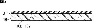
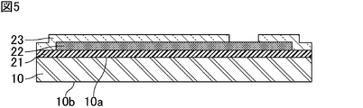
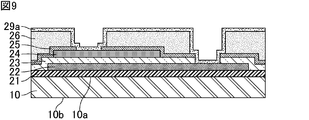
- the semiconductor device 1 shown in FIGS. 1 and 2 is manufactured by, for example, the following method. 3, FIG. 4, FIG. 5, FIG. 6, FIG. 7, FIG. 8, FIG. 9, FIG. 10, FIG. 11, FIG. 12, and FIG. 13 are examples of the method for manufacturing the semiconductor device according to the first embodiment of the present invention. It is a cross-sectional schematic diagram for demonstrating.
- the insulating layer 21 is formed on the first main surface 10a of the semiconductor substrate 10 by, for example, a thermal oxidation method, a sputtering method, or a chemical vapor deposition method.
- a conductor layer made of a constituent material of the first electrode layer 22 is formed on the surface of the insulating layer 21 opposite to the semiconductor substrate 10 by, for example, a sputtering method. After that, the patterning of the conductor layer is performed by combining the photolithography method and the etching method to form the first electrode layer 22 as shown in FIG. More specifically, the first electrode layer 22 is formed up to a position separated from the end portion of the semiconductor substrate 10.
- a layer made of a constituent material of the dielectric layer 23 is formed so as to cover the first electrode layer 22 by, for example, a sputtering method or a chemical vapor deposition method. After that, the patterning of this layer is performed, for example, by combining a photolithography method and an etching method to form the dielectric layer 23 as shown in FIG. More specifically, the dielectric layer 23 is formed so that an opening for exposing a part of the first electrode layer 22 is provided.
- a conductor layer made of a constituent material of the second electrode layer 24 is formed on the surface of the structure shown in FIG. 5 opposite to the semiconductor substrate 10 by, for example, a sputtering method. After that, the patterning of the conductor layer is performed, for example, by combining a photolithography method and an etching method to form the second electrode layer 24 as shown in FIG. More specifically, the second electrode layer 24 is formed so as to face the first electrode layer 22 with the dielectric layer 23 interposed therebetween.
- a layer made of the constituent material of the moisture-resistant protective layer 25 is formed on the surface of the structure shown in FIG. 6 opposite to the semiconductor substrate 10 by, for example, a chemical vapor deposition method. After that, the patterning of this layer is performed, for example, by combining a photolithography method and an etching method to form a moisture-resistant protective layer 25 as shown in FIG. 7. More specifically, an opening is provided at each of a position overlapping the opening of the dielectric layer 23 for exposing a part of the first electrode layer 22 and a position for exposing a part of the second electrode layer 24. As described above, the moisture-resistant protective layer 25 is formed.
- a layer made of the constituent material of the resin protective layer 26 is formed on the surface of the structure shown in FIG. 7 opposite to the semiconductor substrate 10 by, for example, a spin coating method. After that, the patterning of this layer is performed, for example, by using only the photolithography method when the constituent material of the resin protective layer 26 is photosensitive, and when the constituent material of the resin protective layer 26 is non-photolithographic.
- the resin protective layer 26 as shown in FIG. 8 is formed. More specifically, the position overlapping the openings of the dielectric layer 23 and the moisture-resistant protective layer 25 for exposing a part of the first electrode layer 22, and the moisture-resistant protection for exposing a part of the second electrode layer 24.
- the resin protective layer 26 is formed so that an opening is provided at each position overlapping the opening of the layer 25.
- the seed layer 29a is formed on the surface of the structure shown in FIG. 8 opposite to the semiconductor substrate 10. Then, by combining the plating treatment and the photolithography method, the first plating layer 29b and the second plating layer 29c as shown in FIG. 10 are sequentially formed. Then, as shown in FIG. 11, a part of the seed layer 29a is removed by, for example, an etching method. As a result, the first external electrode 27 and the second external electrode 28 as shown in FIG. 11 are formed. More specifically, the first outer surface is electrically connected to the first electrode layer 22 through the openings provided in the dielectric layer 23, the moisture-resistant protective layer 25, and the resin protective layer 26, respectively. The electrode 27 is formed. Further, the second external electrode 28 is formed so as to be electrically connected to the second electrode layer 24 through the openings provided in the moisture resistant protective layer 25 and the resin protective layer 26, respectively.
- the circuit layer 20 as shown in FIG. 11 is formed on the first main surface 10a of the semiconductor substrate 10.
- the first external electrode 27 is drawn out to the surface of the circuit layer 20 opposite to the semiconductor substrate 10, and is separated from the second external electrode 28.
- the second external electrode 28 is drawn out to the surface of the circuit layer 20 opposite to the semiconductor substrate 10 and is separated from the first external electrode 27.
- the photosensitive resin film 35 is formed on the surface of the circuit layer 20 opposite to the semiconductor substrate 10. Then, the photosensitive resin film 35 is patterned by a photolithography method to form the first resin body 30 as shown in FIG. 13 on the surface of the circuit layer 20 opposite to the semiconductor substrate 10. More specifically, it is provided between the first external electrode 27 and the second external electrode 28 in a plan view, and the tip on the side opposite to the semiconductor substrate 10 in a cross-sectional view is the first external electrode 27 and The first resin body 30 is formed so as to be located higher than the tip of the second external electrode 28 on the side opposite to the semiconductor substrate 10. Further, in a plan view, the first resin body 30 is formed so as to be provided at at least three positions surrounding the center of the semiconductor substrate 10.
- the semiconductor device 1 as shown in FIG. 13 is manufactured.
- the semiconductor substrate 10 is cut by dicing or the like.
- a plurality of semiconductor devices 1 may be manufactured at the same time by individualizing them.
- the module of the present invention comprises a semiconductor device of the present invention, a wiring board having a first land electrically connected to a first external electrode, and a second land electrically connected to a second external electrode. It is characterized by having.
- the module having the semiconductor device according to the first embodiment of the present invention will be described as the module according to the first embodiment of the present invention.
- FIG. 14 is a schematic cross-sectional view showing the module of the first embodiment of the present invention.
- the module 100 includes a semiconductor device 1 and a wiring board 50. More specifically, in the module 100, the semiconductor device 1 is mounted on the wiring board 50.
- the wiring board 50 has a board 51, a first land 52, and a second land 53.
- Various wirings are provided on the board 51.
- the various wirings of the board 51 are independently connected to the first land 52 and the second land 53.
- the first land 52 is provided on the surface of the substrate 51 and is electrically connected to the first external electrode 27. More specifically, the first land 52 is electrically connected to the first external electrode 27 via the solder 60.
- Examples of the constituent material of the first land 52 include a metal such as copper (Cu).
- the second land 53 is provided at a position separated from the first land 52 on the surface of the substrate 51, and is electrically connected to the second external electrode 28. More specifically, the second land 53 is electrically connected to the second external electrode 28 via the solder 60.
- Examples of the constituent material of the second land 53 include a metal such as copper (Cu).
- the first resin body 30 is not in contact with the wiring board 50 side (for example, the first land 52, the second land 53, the solder 60, etc.), but this is considered to be due to, for example, the following mechanism. Be done.
- the first mechanism a case where the semiconductor device 1 is mounted on the wiring board 50 without being displaced will be described.
- the semiconductor device 1 is mounted on the wiring board 50 via the solder 60
- the first resin body 30 first comes into contact with the solder 60.
- the solder 60 gets wet and spreads as a whole in each of the first land 52 and the second land 53, but the solder 60 avoids the first resin body 30, and as a result, the first The resin body 30 does not come into contact with the solder 60.
- the semiconductor device 1 is mounted on the wiring board 50 in a displaced state.
- the self-alignment effect during the reflow process results in the first resin body 30 not coming into contact with the solder 60.
- FIG. 15 is a schematic cross-sectional view showing a state in which the mold resin is provided in the module of the first embodiment of the present invention.
- the first resin body includes a wall portion extending in a direction orthogonal to the thickness direction and intersecting a direction from the second external electrode to the first external electrode. You may. Such an example will be described below as a semiconductor device according to the second embodiment of the present invention.
- the semiconductor device according to the second embodiment of the present invention is the same as the semiconductor device according to the first embodiment of the present invention, except that the configuration of the first resin body is changed.
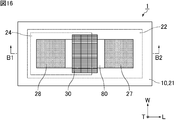
- FIG. 16 is a schematic plan view showing the semiconductor device according to the second embodiment of the present invention.
- FIG. 17 is a schematic cross-sectional view showing a portion corresponding to the line segments B1-B2 in FIG.
- the first resin body 30 is in a direction orthogonal to the thickness direction T and is directed from the second external electrode 28 to the first external electrode 27, in this case, the length direction L. Includes a wall that extends in the direction of intersection with respect to. More specifically, the first resin body 30 includes a wall portion extending in a direction orthogonal to both the length direction L and the thickness direction T, that is, the width direction W.
- the first resin body 30 includes such a wall portion, for example, when the semiconductor device 1 is mounted on the wiring board, the load can be more widely distributed by the first resin body 30, so that the capacitor element, particularly the dielectric, is used. The load applied to the layer 23 is sufficiently suppressed.
- both the dimension in the length direction L and the dimension in the width direction W of the first resin body 30 are preferably 3 ⁇ m or more.
- both the dimension in the length direction L and the dimension in the width direction W of the first resin body 30 are shorter than 3 ⁇ m, when the semiconductor device 1 is mounted on the wiring board, the first resin body 30 receives the load while receiving the load.
- the semiconductor substrate 10 and the circuit layer 20 may not be stably held on the wiring board.
- the dimensions of the first resin body 30 in the width direction W in the plan view as shown in FIG. 16 are as follows. It is preferable that the dimensions of the first external electrode 27 and the second external electrode 28 are longer than the dimensions in the width direction W of each.
- the first resin body 30 has a rectangular shape, but its shape is not particularly limited, and may be, for example, an elliptical shape.
- the module of the second embodiment of the present invention is the same as the module of the first embodiment of the present invention except that it has the semiconductor device of the second embodiment of the present invention.
- the first resin body 30 as a wall portion extends to a region 80 connecting the opposite ends of the first external electrode 27 and the second external electrode 28.
- the wall portion is a first wall portion provided on the first external electrode side and a second wall portion provided on the second external electrode side and separated from the first wall portion. And may include. Such an example will be described below as a semiconductor device according to the first modification of the second embodiment of the present invention.
- FIG. 18 is a schematic plan view showing the semiconductor device of the first modification of the second embodiment of the present invention.
- FIG. 19 is a schematic cross-sectional view showing a portion corresponding to the line segments C1-C2 in FIG.
- the first resin body 30 as the wall portion is provided on the first wall portion 30a provided on the first external electrode 27 side and on the second external electrode 28 side, and is the first.
- a second wall portion 30b separated from the wall portion 30a is included.
- the semiconductor substrate is formed by the first resin body 30. 10 and the circuit layer 20 can be stably held on the wiring board. Further, for example, when the semiconductor device 1 is mounted on the wiring board, the load can be more widely dispersed by the first resin body 30, so that the load applied to the capacitor element, particularly the dielectric layer 23, is sufficiently suppressed.
- one end of the first wall portion 30a and the second wall portion 30b is an end portion of the first external electrode 27 and the second external electrode 28 facing each other, respectively. It is preferably located between one end of the region 80 connecting the two and one end of the semiconductor substrate 10. Further, in the width direction W, the other ends of the first wall portion 30a and the second wall portion 30b are the other ends of the region 80 connecting the opposite ends of the first external electrode 27 and the second external electrode 28, respectively. And preferably located between the other end of the semiconductor substrate 10.
- the dimensions of the first wall portion 30a and the second wall portion 30b in the length direction L are preferably each. It is 3 ⁇ m or more. Further, the dimensions of the first wall portion 30a and the second wall portion 30b in the length direction L are preferably less than half of the distance between the first external electrode 27 and the second external electrode 28 in the length direction L, respectively. be.
- the dimensions of the first wall portion 30a and the second wall portion 30b in the width direction W are preferably 10 ⁇ m, respectively. That is all.
- the dimensions of the first wall portion 30a and the second wall portion 30b in the width direction W are preferably equal to or less than the dimensions of the semiconductor substrate 10 in the width direction W, respectively.
- the first wall portion 30a and the second wall portion 30b are provided in parallel.
- the semiconductor substrate 10 and the circuit layer 20 can be sufficiently stably held on the wiring board by the first resin body 30.
- the first wall portion 30a is provided on one side with respect to the center thereof, and the second wall portion 30b is provided on the other side, whereby the first resin is provided.
- the body 30 can hold the semiconductor substrate 10 and the circuit layer 20 more stably on the wiring board.
- the distance L1 between the first wall portion 30a and the first external electrode 27 is shorter than the distance L2 between the center position Z between the first external electrode 27 and the second external electrode 28 and the first wall portion 30a, and is shorter than the distance L2 between the first wall portion 30a and the first external electrode 28.
- the distance L3 between the portion 30b and the second external electrode 28 is preferably shorter than the distance L4 between the center position Z between the first external electrode 27 and the second external electrode 28 and the second wall portion 30b.
- the distance L1, the distance L2, the distance L3, the distance L4, and the center position Z are each determined as follows. First, a midpoint between the opposite ends of the first external electrode 27 and the second external electrode 28 is determined on each of the five straight lines extending in the length direction L, and the straight line connecting these midpoints is centered. Determined as position Z.
- position Z the straight line passing through the position where the distance between the first wall portion 30a and the first external electrode 27 is maximized, and the distance between the first wall portion 30a and the first external electrode 27.
- the average value of the obtained five measured values is defined as the distance L1, the distance L2, the distance L3, and the distance L4, respectively.
- the first wall portion 30a and the second wall portion 30b are made of, for example, a solder-repellent material such as solder resist
- the first wall portion 30a and the second wall portion 30b are the first external electrode 27 and the first wall portion 30b.
- the semiconductor device 1 more specifically, each of the first external electrode 27 and the second external electrode 28
- a large constriction is made on each electrode of the first external electrode 27 and the second external electrode 28 so that the solder avoids the first wall portion 30a and the second wall portion 30b. It may end up.
- the bonding strength of the solder to each of the first external electrode 27 and the second external electrode 28 may decrease.
- the solder is greatly constricted, disconnection in the solder is likely to occur.
- the current path becomes the outer peripheral portion of the solder due to the skin effect, but when the solder is greatly constricted, the current path becomes long, resulting in an equivalent series resistance (ESR). It rises and the Q value worsens. From the viewpoint of suppressing such a defect, it is preferable that the first wall portion 30a and the first external electrode 27 are separated from each other, and the second wall portion 30b and the second external electrode 28 are separated from each other.
- the module of the first modification of the second embodiment of the present invention is the same as the module of the first embodiment of the present invention except that it has the semiconductor device of the first modification of the second embodiment of the present invention.
- the second resin body is provided on the surface of the circuit layer opposite to the semiconductor substrate, and the second resin body is the end portion of the semiconductor substrate and the first resin body in a plan view. It is provided along the edge of the semiconductor substrate between the first outer peripheral portion provided along the edge of the semiconductor substrate between the external electrode and the end of the semiconductor substrate and the second external electrode in a plan view. It may have a second outer peripheral portion and the like. Such an example will be described below as a semiconductor device according to a modification 2 of the second embodiment of the present invention.
- the semiconductor device of the second modification of the second embodiment of the present invention a case where the first resin body includes the first wall portion and the second wall portion as the wall portion is exemplified. That is, the semiconductor device of the second modification of the second embodiment of the present invention is the same as the semiconductor device of the first modification of the second embodiment of the present invention except that the second resin body is provided.
- FIG. 20 is a schematic plan view showing the semiconductor device of the second modification of the second embodiment of the present invention.
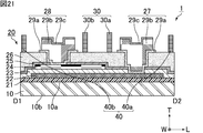
- FIG. 21 is a schematic cross-sectional view showing a portion corresponding to the line segments D1-D2 in FIG. 20.
- a second resin body 40 is provided on the surface of the circuit layer 20 opposite to the semiconductor substrate 10.
- the second resin body 40 has a first outer peripheral portion 40a provided along the end portion of the semiconductor substrate 10 between the end portion of the semiconductor substrate 10 and the first external electrode 27 in a plan view as shown in FIG.
- a second outer peripheral portion 40b provided along the end portion of the semiconductor substrate 10 is provided between the end portion of the semiconductor substrate 10 and the second external electrode 28 in a plan view as shown in FIG. 20.
- the first outer peripheral portion 40a includes both ends extending along the length direction L of the semiconductor substrate 10 and one end extending along the width direction W around the first external electrode 27. It is provided along.
- the second outer peripheral portion 40b is provided around the second external electrode 28 along both ends extending along the length direction L and the other ends extending along the width direction W of the semiconductor substrate 10. ing.
- the semiconductor device 1 is cut so as to include the second resin body 40, so that it is possible to suppress the occurrence of chipping in the semiconductor device 1.
- the tip of the second resin body 40 on the opposite side of the semiconductor substrate 10 here, the tip of the first outer peripheral portion 40a and the second outer peripheral portion 40b on the opposite side of the semiconductor substrate 10.
- the tip of the first resin body 30 on the opposite side of the semiconductor substrate 10 here, at a position lower than the tip of the first wall portion 30a and the second wall portion 30b on the opposite side of the semiconductor substrate 10. preferable.
- the semiconductor substrate 10 and the circuit layer 20 can be stably held on the wiring board by the first resin body 30.
- the end portion of the circuit layer 20 is more likely to be lowered toward the semiconductor substrate 10 side than the central portion. Therefore, the tip of the second resin body 40 on the opposite side of the semiconductor substrate 10 tends to be lower than the tip of the first resin body 30 on the opposite side of the semiconductor substrate 10.
- the tip of the second resin body 40 on the opposite side of the semiconductor substrate 10, here, the tip of the first outer peripheral portion 40a and the second outer peripheral portion 40b on the opposite side of the semiconductor substrate 10. is preferably located at a position higher than the tip of the first external electrode 27 and the second external electrode 28 on the opposite side of the semiconductor substrate 10.
- the load can be more widely distributed by the second resin body 40, so that the load applied to the capacitor element, particularly the dielectric layer 23, is sufficiently suppressed.
- the second resin body having the first outer peripheral portion and the second outer peripheral portion may be provided in the semiconductor device according to the first embodiment of the present invention.
- the module of the second modification of the second embodiment of the present invention is the same as the module of the first embodiment of the present invention except that it has the semiconductor device of the second modification of the second embodiment of the present invention.
- the side surface of the wall portion on the first external electrode side and the side surface of the wall portion on the second external electrode side are from the semiconductor substrate side to the side opposite to the semiconductor substrate. They may be approaching each other.
- Such an example will be described below as a semiconductor device according to a modification 3 of the second embodiment of the present invention.
- the semiconductor device of the third modification of the second embodiment of the present invention a case where the first resin body includes the first wall portion and the second wall portion as the wall portion is exemplified. That is, the semiconductor device of the third modification of the second embodiment of the present invention is the same as the semiconductor device of the second modification of the second embodiment of the present invention, except that the shape of the first resin body is changed.
- FIG. 22 is a schematic cross-sectional view showing the semiconductor device of the third modification of the second embodiment of the present invention.
- the side surface of the first wall portion 30a on the first external electrode 27 side and the side surface of the first wall portion 30a on the second external electrode 28 side are from the semiconductor substrate 10 side to the semiconductor substrate 10. They are approaching each other toward the opposite side.
- the side surface of the second wall portion 30b on the first external electrode 27 side and the side surface of the second wall portion 30b on the second external electrode 28 side are semiconductors from the semiconductor substrate 10 side. They are approaching each other toward the opposite side of the substrate 10.
- the cross-sectional shapes of the first wall portion 30a and the second wall portion 30b are so-called tapered shapes in which the width decreases from the semiconductor substrate 10 side toward the side opposite to the semiconductor substrate 10, respectively.
- the side surface on the first external electrode 27 side and the side surface on the second external electrode 28 side are from the semiconductor substrate 10 side toward the side opposite to the semiconductor substrate 10. As long as they are close to each other, they may be curved.
- the first wall portion 30a and the second wall portion 30b have the above-mentioned shapes, the first wall portion 30a and the region on the first external electrode 27 are farther from each other as compared with the state shown in FIG. , The second wall portion 30b and the region on the second external electrode 28 become far apart. Therefore, when the semiconductor device 1, more specifically, each of the first external electrode 27 and the second external electrode 28 is connected to the land of the wiring board via solder, the first wall portion 30a and the second wall portion 30a and the second wall portion are connected. Even when 30b is made of a material that repels solder, such as a solder resist, the solder does not constrict significantly on each of the first external electrode 27 and the second external electrode 28.
- the current path of the solder connecting each of the first external electrode 27 and the second external electrode 28 and the land of the wiring board is not narrowed in the middle.
- the decrease in the bonding strength of the solder with respect to each of the first external electrode 27 and the second external electrode 28 is sufficiently suppressed.
- the solder does not constrict significantly, disconnection in the solder is less likely to occur.
- the semiconductor device 1 is used in a high frequency region, the current path becomes the outer peripheral portion of the solder due to the skin effect, but the current path does not become long because the solder does not constrict greatly, and as a result, the equivalent series resistance. And the deterioration of the Q value are suppressed.
- FIG. 22 shows.
- the distance between the side surface of the first wall portion 30a on the side of the first external electrode 27 and the first external electrode 27 increases from the semiconductor substrate 10 side toward the side opposite to the semiconductor substrate 10. That is, when the first resin body 30 includes a plurality of wall portions, the wall portion provided on the side of the first external electrode 27 among the plurality of wall portions, here, the first external electrode of the first wall portion 30a.
- the distance between the side surface on the 27 side and the first external electrode 27 increases from the semiconductor substrate 10 side toward the side opposite to the semiconductor substrate 10. If the side surface of the first wall portion 30a on the side of the first external electrode 27 and the side surface of the second external electrode 28 are close to each other from the semiconductor substrate 10 side toward the side opposite to the semiconductor substrate 10. The distance between the side surface of the first wall portion 30a on the second external electrode 28 side and the first external electrode 27 may be smaller from the semiconductor substrate 10 side toward the side opposite to the semiconductor substrate 10 or is constant. There may be. In other words, the distance between the side surface of the first wall portion 30a on the side of the second external electrode 28 and the second external electrode 28 may increase from the semiconductor substrate 10 side toward the side opposite to the semiconductor substrate 10. , May be constant.
- the second wall portion 30b and the region on the second external electrode 28 are separated from each other.
- the distance between the side surface of the second wall portion 30b on the second external electrode 28 side and the second external electrode 28 is preferably increased from the semiconductor substrate 10 side toward the side opposite to the semiconductor substrate 10. .. That is, when the first resin body 30 includes a plurality of wall portions, the wall portion provided on the side of the second external electrode 28 among the plurality of wall portions, here, the second external electrode of the second wall portion 30b. It is preferable that the distance between the side surface on the 28 side and the second external electrode 28 increases from the semiconductor substrate 10 side toward the side opposite to the semiconductor substrate 10.
- the distance between the side surface of the second wall portion 30b on the side of the first external electrode 27 and the side surface of the second external electrode 28 may be smaller from the semiconductor substrate 10 side toward the side opposite to the semiconductor substrate 10 or is constant. There may be. In other words, the distance between the side surface of the second wall portion 30b on the side of the first external electrode 27 and the first external electrode 27 may increase from the semiconductor substrate 10 side toward the side opposite to the semiconductor substrate 10. , May be constant.
- the distance between the side surface of the first resin body 30 on the first external electrode 27 side and the first external electrode 27 is preferable that the distance between the side surface of the first resin body 30 on the second external electrode 28 side and the second external electrode 28 increases from the semiconductor substrate 10 side toward the side opposite to the semiconductor substrate 10.
- the first outer peripheral portion 40a and the second outer peripheral portion 40b as shown in FIG. 22 are similar to the semiconductor device of the second modification of the second embodiment of the present invention.
- the second resin body 40 having the above may be provided.
- the cross-sectional shapes of the first outer peripheral portion 40a and the second outer peripheral portion 40b are respectively from the semiconductor substrate 10 side. It is preferable that the width becomes smaller toward the side opposite to the semiconductor substrate 10.
- the distance between the side surface of the first outer peripheral portion 40a on the side of the first external electrode 27 and the first external electrode 27 may increase from the semiconductor substrate 10 side toward the side opposite to the semiconductor substrate 10.
- the distance between the side surface of the second outer peripheral portion 40b on the side of the second external electrode 28 and the second external electrode 28 increases from the semiconductor substrate 10 side toward the side opposite to the semiconductor substrate 10.
- the module of the third modification of the second embodiment of the present invention is the same as the module of the first embodiment of the present invention except that it has the semiconductor device of the third modification of the second embodiment of the present invention.
- the second resin body is provided on the surface of the circuit layer opposite to the semiconductor substrate, and the second resin body is the edge of the semiconductor substrate in a plan view. It has a first outer peripheral portion provided between the portion and the first external electrode, and a second outer peripheral portion provided between the end portion of the semiconductor substrate and the second external electrode in a plan view.
- the 1st wall portion and the 1st outer peripheral portion are connected to each other, the 2nd wall portion and the 2nd outer peripheral portion are connected to each other, and the 1st wall portion communicates with the space separating the 1st wall portion and the 2nd outer peripheral portion.
- the first opening may be provided, and the second wall portion may be provided with a second opening communicating with the space separating the first wall portion and the second wall portion.
- FIG. 23 is a schematic plan view showing the semiconductor device of the modified example 4 of the second embodiment of the present invention.
- a second resin body 40 is provided on the surface of the circuit layer 20 opposite to the semiconductor substrate 10.
- the second resin body 40 has a first outer peripheral portion 40a provided between an end portion of the semiconductor substrate 10 and the first external electrode 27 in a plan view as shown in FIG. 23, and a plan view as shown in FIG. 23. It has a second outer peripheral portion 40b provided between the end portion of the semiconductor substrate 10 and the second external electrode 28.
- the first outer peripheral portion 40a extends along the end portion of the semiconductor substrate 10, more specifically, around the first external electrode 27, along the length direction L of the semiconductor substrate 10, and both ends and the width direction. It may be provided along one end extending along W and along.
- the second outer peripheral portion 40b extends along the end portion of the semiconductor substrate 10, more specifically, around the second external electrode 28, along the length direction L of the semiconductor substrate 10, and both ends and the width direction. It may be provided along the other end extending along W.
- the first wall portion 30a and the first outer peripheral portion 40a are connected to each other. Further, the second wall portion 30b and the second outer peripheral portion 40b are connected to each other.
- the first wall portion 30a is provided with a first opening 31a that communicates with a space that separates the first wall portion 30a and the second wall portion 30b. Further, the second wall portion 30b is provided with a second opening 31b that communicates with the space that separates the first wall portion 30a and the second wall portion 30b.
- the semiconductor device 1 Since the first opening 31a and the second opening 31b are provided in the first wall portion 30a and the second wall portion 30b, respectively, when the semiconductor device 1 is mounted on the wiring board to form a module, the semiconductor device 1 When the mold resin is filled in the space separating the first wall portion 30a and the second wall portion 30b after mounting the above on the wiring board, the periphery of the first external electrode 27 is passed through the first opening 31a communicating with the space. In addition, it becomes easy to fill the periphery of the second external electrode 28 through the second opening 31b.
- the tip of the 40b opposite to the semiconductor substrate 10 is the tip of the first resin body 30 opposite to the semiconductor substrate 10, where the first wall portion 30a and the second wall portion 30b are opposite to the semiconductor substrate 10. It is preferably located lower than the tip on the side.
- the module of the modified example 4 of the second embodiment of the present invention is the same as the module of the first embodiment of the present invention except that it has the semiconductor device of the modified example 4 of the second embodiment of the present invention.
- the wall portion may extend to a region connecting the opposite ends of the first external electrode and the second external electrode.
- the wall portion may extend to a region connecting the opposite ends of the first external electrode and the second external electrode.
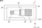
- FIG. 24 is a schematic plan view showing a semiconductor device according to a modification 5 of the second embodiment of the present invention.
- the first resin body 30 as a wall portion extends to a region 80 connecting the opposite ends of the first external electrode 27 and the second external electrode 28.
- FIG. 25 is a schematic cross-sectional view showing the module of the modified example 5 of the second embodiment of the present invention.
- the module of the second embodiment of the present invention is the same as the module of the first embodiment of the present invention except that it has the semiconductor device of the fifth modification of the second embodiment of the present invention. Since the first resin body 30 extends to the region 80 in the plan view as shown in FIG. 24, when the semiconductor device 1 is mounted on the wiring board 50 to form the module 100 as shown in FIG. 25, Even if the solder 60 gets wet and spreads, that is, a so-called solder splash occurs, the wet and spread path of the solder 60 becomes longer by the amount of the first resin body 30, as shown by the arrows in FIG. 25. Therefore, it is possible to suppress a short circuit between the first external electrode 27 and the second external electrode 28 due to the solder splash.
- Such an action effect can be similarly obtained when the semiconductor device 1 shown in FIGS. 16, 18 and 20 is mounted on a wiring board to form a module.
- the wall portion is provided on the first external electrode side and the second external electrode side, and is separated from the first wall portion.
- a second resin body is provided on the surface of the circuit layer opposite to the semiconductor substrate, including the second wall portion, and the second resin body is the end portion of the semiconductor substrate and the first outer surface in a plan view. It has a first outer peripheral portion provided between the electrodes and a second outer peripheral portion provided between the end portion of the semiconductor substrate and the second external electrode in a plan view, and has a first wall portion and a first outer peripheral portion.
- the outer peripheral portion is connected, the second wall portion and the second outer peripheral portion are connected, and the first wall portion has a first opening that communicates with the space that separates the first wall portion and the second wall portion.
- the second wall portion is provided with a second opening that communicates with the space that separates the first wall portion and the second wall portion, and the first wall portion is provided in the direction from the second external electrode to the first external electrode.
- the opening may face the second wall and the second opening may face the first wall.
- FIG. 26 is a schematic plan view showing a semiconductor device according to a modification 6 of the second embodiment of the present invention.
- the first resin body 30 as the wall portion is provided on the first wall portion 30a provided on the first external electrode 27 side and the first wall portion 30a provided on the second external electrode 28 side.
- the second wall portion 30b which is separated from the above, is included.
- a second resin body 40 is provided on the surface of the circuit layer 20 opposite to the semiconductor substrate 10.
- the second resin body 40 has a first outer peripheral portion 40a provided between the end portion of the semiconductor substrate 10 and the first external electrode 27 in a plan view as shown in FIG. 26, and a plan view as shown in FIG. 26. It has a second outer peripheral portion 40b provided between the end portion of the semiconductor substrate 10 and the second external electrode 28.
- the first outer peripheral portion 40a extends along the end portion of the semiconductor substrate 10, more specifically, around the first external electrode 27, along the length direction L of the semiconductor substrate 10, and both ends and the width direction. It may be provided along one end extending along W and along.
- the second outer peripheral portion 40b extends along the end portion of the semiconductor substrate 10, more specifically, around the second external electrode 28, along the length direction L of the semiconductor substrate 10, and both ends and the width direction. It may be provided along the other end extending along W.
- the first wall portion 30a and the first outer peripheral portion 40a are connected to each other. Further, the second wall portion 30b and the second outer peripheral portion 40b are connected to each other.
- the first wall portion 30a is provided with a first opening 31a that communicates with a space that separates the first wall portion 30a and the second wall portion 30b. Further, the second wall portion 30b is provided with a second opening 31b that communicates with the space that separates the first wall portion 30a and the second wall portion 30b.
- the first opening 31a faces the second wall portion 30b
- the second opening 31b faces the first wall portion 30a. Facing each other.
- the semiconductor device 1 Since the first opening 31a and the second opening 31b are provided in the first wall portion 30a and the second wall portion 30b, respectively, when the semiconductor device 1 is mounted on the wiring board to form a module, the semiconductor device 1 When the mold resin is filled in the space separating the first wall portion 30a and the second wall portion 30b after mounting the above on the wiring board, the periphery of the first external electrode 27 is passed through the first opening 31a communicating with the space. In addition, it becomes easy to fill the periphery of the second external electrode 28 through the second opening 31b.
- the first opening 31a faces the second wall portion 30b and the second opening 31b faces the first wall portion 30a, that is, the first opening 31a and the second opening Since the 31bs do not face each other, even if a solder splash occurs when the semiconductor device 1 is mounted on the wiring board to form a module, the first wall portion 30a and the second wall portion 30b serve as barriers. A short circuit between the first external electrode 27 and the second external electrode 28 can be suppressed.
- the tip of the 40b opposite to the semiconductor substrate 10 is the tip of the first resin body 30 opposite to the semiconductor substrate 10, where the first wall portion 30a and the second wall portion 30b are opposite to the semiconductor substrate 10. It is preferably located lower than the tip on the side.
- the module of the modified example 6 of the second embodiment of the present invention is the same as the module of the first embodiment of the present invention except that it has the semiconductor device of the modified example 6 of the second embodiment of the present invention.
Landscapes
- Engineering & Computer Science (AREA)
- Power Engineering (AREA)
- Microelectronics & Electronic Packaging (AREA)
- Manufacturing & Machinery (AREA)
- Chemical & Material Sciences (AREA)
- Materials Engineering (AREA)
- Inorganic Chemistry (AREA)
- Internal Circuitry In Semiconductor Integrated Circuit Devices (AREA)
- Ceramic Capacitors (AREA)
- Fixed Capacitors And Capacitor Manufacturing Machines (AREA)
- Semiconductor Integrated Circuits (AREA)
Priority Applications (3)
| Application Number | Priority Date | Filing Date | Title |
|---|---|---|---|
| CN202180014437.9A CN115088071A (zh) | 2020-02-17 | 2021-02-16 | 半导体装置以及模块 |
| JP2022501894A JP7388536B2 (ja) | 2020-02-17 | 2021-02-16 | 半導体装置及びモジュール |
| US17/880,113 US12464740B2 (en) | 2020-02-17 | 2022-08-03 | Semiconductor device and module |
Applications Claiming Priority (2)
| Application Number | Priority Date | Filing Date | Title |
|---|---|---|---|
| JP2020-024563 | 2020-02-17 | ||
| JP2020024563 | 2020-02-17 |
Related Child Applications (1)
| Application Number | Title | Priority Date | Filing Date |
|---|---|---|---|
| US17/880,113 Continuation US12464740B2 (en) | 2020-02-17 | 2022-08-03 | Semiconductor device and module |
Publications (1)
| Publication Number | Publication Date |
|---|---|
| WO2021166880A1 true WO2021166880A1 (ja) | 2021-08-26 |
Family
ID=77392098
Family Applications (1)
| Application Number | Title | Priority Date | Filing Date |
|---|---|---|---|
| PCT/JP2021/005626 Ceased WO2021166880A1 (ja) | 2020-02-17 | 2021-02-16 | 半導体装置及びモジュール |
Country Status (4)
| Country | Link |
|---|---|
| US (1) | US12464740B2 (https=) |
| JP (1) | JP7388536B2 (https=) |
| CN (1) | CN115088071A (https=) |
| WO (1) | WO2021166880A1 (https=) |
Cited By (2)
| Publication number | Priority date | Publication date | Assignee | Title |
|---|---|---|---|---|
| JPWO2023106083A1 (https=) * | 2021-12-08 | 2023-06-15 | ||
| JP2025511636A (ja) * | 2022-04-24 | 2025-04-16 | ホアウェイ・テクノロジーズ・カンパニー・リミテッド | コンデンサ、及びコンデンサを製造する方法 |
Families Citing this family (2)
| Publication number | Priority date | Publication date | Assignee | Title |
|---|---|---|---|---|
| DE112022002407T5 (de) * | 2021-05-03 | 2024-02-15 | KYOCERA AVX Components Corporation | Metalloxidhalbleiter-kondensator und leiterplatte, in der ein solcher eingebettet ist |
| JP7758341B2 (ja) * | 2022-03-07 | 2025-10-22 | 住友電工デバイス・イノベーション株式会社 | キャパシタおよびその製造方法 |
Citations (2)
| Publication number | Priority date | Publication date | Assignee | Title |
|---|---|---|---|---|
| WO2016021529A1 (ja) * | 2014-08-06 | 2016-02-11 | 株式会社村田製作所 | 複合電子部品 |
| WO2017057422A1 (ja) * | 2015-10-02 | 2017-04-06 | 株式会社村田製作所 | 薄膜型lc部品およびその実装構造 |
Family Cites Families (6)
| Publication number | Priority date | Publication date | Assignee | Title |
|---|---|---|---|---|
| JP5234521B2 (ja) | 2009-08-21 | 2013-07-10 | Tdk株式会社 | 電子部品及びその製造方法 |
| WO2014192430A1 (ja) * | 2013-05-31 | 2014-12-04 | 株式会社村田製作所 | 半導体装置 |
| JP6319467B2 (ja) * | 2015-02-12 | 2018-05-09 | 株式会社村田製作所 | 薄膜デバイス |
| CN112041954B (zh) * | 2018-04-27 | 2022-08-02 | 株式会社村田制作所 | 电容器集合体 |
| JP2020004886A (ja) * | 2018-06-29 | 2020-01-09 | 太陽誘電株式会社 | 半導体モジュール |
| JP7197001B2 (ja) * | 2019-05-13 | 2022-12-27 | 株式会社村田製作所 | キャパシタ |
-
2021
- 2021-02-16 CN CN202180014437.9A patent/CN115088071A/zh active Pending
- 2021-02-16 JP JP2022501894A patent/JP7388536B2/ja active Active
- 2021-02-16 WO PCT/JP2021/005626 patent/WO2021166880A1/ja not_active Ceased
-
2022
- 2022-08-03 US US17/880,113 patent/US12464740B2/en active Active
Patent Citations (2)
| Publication number | Priority date | Publication date | Assignee | Title |
|---|---|---|---|---|
| WO2016021529A1 (ja) * | 2014-08-06 | 2016-02-11 | 株式会社村田製作所 | 複合電子部品 |
| WO2017057422A1 (ja) * | 2015-10-02 | 2017-04-06 | 株式会社村田製作所 | 薄膜型lc部品およびその実装構造 |
Cited By (4)
| Publication number | Priority date | Publication date | Assignee | Title |
|---|---|---|---|---|
| JPWO2023106083A1 (https=) * | 2021-12-08 | 2023-06-15 | ||
| WO2023106083A1 (ja) * | 2021-12-08 | 2023-06-15 | 株式会社村田製作所 | 半導体装置、マッチング回路及びフィルタ回路 |
| JP7647933B2 (ja) | 2021-12-08 | 2025-03-18 | 株式会社村田製作所 | 半導体装置、マッチング回路及びフィルタ回路 |
| JP2025511636A (ja) * | 2022-04-24 | 2025-04-16 | ホアウェイ・テクノロジーズ・カンパニー・リミテッド | コンデンサ、及びコンデンサを製造する方法 |
Also Published As
| Publication number | Publication date |
|---|---|
| US20220376036A1 (en) | 2022-11-24 |
| JP7388536B2 (ja) | 2023-11-29 |
| CN115088071A (zh) | 2022-09-20 |
| US12464740B2 (en) | 2025-11-04 |
| JPWO2021166880A1 (https=) | 2021-08-26 |
Similar Documents
| Publication | Publication Date | Title |
|---|---|---|
| JP7388536B2 (ja) | 半導体装置及びモジュール | |
| US8416578B2 (en) | Manufacturing method for an electronic substrate | |
| CN110914973B (zh) | 电容器 | |
| CN110800098B (zh) | 薄膜电容器及其制造方法 | |
| US10847317B2 (en) | Electronic component | |
| JP7563591B2 (ja) | 半導体装置、マッチング回路及びフィルタ回路 | |
| US12424389B2 (en) | Semiconductor device and capacitance device | |
| JP7647880B2 (ja) | 半導体装置 | |
| US20220181277A1 (en) | Semiconductor device package | |
| JP7683684B2 (ja) | 半導体装置及びモジュール | |
| US20240063252A1 (en) | Semiconductor device and module | |
| KR20070037826A (ko) | 차폐된 재배선층을 갖는 웨이퍼 레벨 칩 스케일 패키지 | |
| CN113644040B (zh) | 封装结构及其形成方法 | |
| KR101217356B1 (ko) | 반도체 디바이스의 제조 방법 및 이를 이용한 반도체 디바이스 | |
| JP2006344850A (ja) | 電子部品 | |
| JP2009277879A (ja) | 半導体装置 | |
| JP2015103776A (ja) | 多層配線用パッド構造 | |
| JP2002110453A (ja) | 薄膜電子部品および基板 | |
| JP2003347156A (ja) | 薄膜電子部品 |
Legal Events
| Date | Code | Title | Description |
|---|---|---|---|
| 121 | Ep: the epo has been informed by wipo that ep was designated in this application |
Ref document number: 21757793 Country of ref document: EP Kind code of ref document: A1 |
|
| ENP | Entry into the national phase |
Ref document number: 2022501894 Country of ref document: JP Kind code of ref document: A |
|
| NENP | Non-entry into the national phase |
Ref country code: DE |
|
| 122 | Ep: pct application non-entry in european phase |
Ref document number: 21757793 Country of ref document: EP Kind code of ref document: A1 |