WO2021153609A1 - 半導体装置および半導体装置の製造方法 - Google Patents
半導体装置および半導体装置の製造方法 Download PDFInfo
- Publication number
- WO2021153609A1 WO2021153609A1 PCT/JP2021/002822 JP2021002822W WO2021153609A1 WO 2021153609 A1 WO2021153609 A1 WO 2021153609A1 JP 2021002822 W JP2021002822 W JP 2021002822W WO 2021153609 A1 WO2021153609 A1 WO 2021153609A1
- Authority
- WO
- WIPO (PCT)
- Prior art keywords
- semiconductor
- semiconductor device
- layer
- crystal
- film
- Prior art date
- Legal status (The legal status is an assumption and is not a legal conclusion. Google has not performed a legal analysis and makes no representation as to the accuracy of the status listed.)
- Ceased
Links
Images


Classifications
-
- H—ELECTRICITY
- H10—SEMICONDUCTOR DEVICES; ELECTRIC SOLID-STATE DEVICES NOT OTHERWISE PROVIDED FOR
- H10P—GENERIC PROCESSES OR APPARATUS FOR THE MANUFACTURE OR TREATMENT OF DEVICES COVERED BY CLASS H10
- H10P14/00—Formation of materials, e.g. in the shape of layers or pillars
- H10P14/20—Formation of materials, e.g. in the shape of layers or pillars of semiconductor materials
- H10P14/27—Formation of materials, e.g. in the shape of layers or pillars of semiconductor materials using selective deposition, e.g. simultaneous growth of monocrystalline and non-monocrystalline semiconductor materials
- H10P14/271—Formation of materials, e.g. in the shape of layers or pillars of semiconductor materials using selective deposition, e.g. simultaneous growth of monocrystalline and non-monocrystalline semiconductor materials characterised by the preparation of substrate for selective deposition
- H10P14/272—Formation of materials, e.g. in the shape of layers or pillars of semiconductor materials using selective deposition, e.g. simultaneous growth of monocrystalline and non-monocrystalline semiconductor materials characterised by the preparation of substrate for selective deposition using mask materials other than SiO2 or SiN
-
- H—ELECTRICITY
- H10—SEMICONDUCTOR DEVICES; ELECTRIC SOLID-STATE DEVICES NOT OTHERWISE PROVIDED FOR
- H10D—INORGANIC ELECTRIC SEMICONDUCTOR DEVICES
- H10D8/00—Diodes
- H10D8/60—Schottky-barrier diodes
-
- C—CHEMISTRY; METALLURGY
- C23—COATING METALLIC MATERIAL; COATING MATERIAL WITH METALLIC MATERIAL; CHEMICAL SURFACE TREATMENT; DIFFUSION TREATMENT OF METALLIC MATERIAL; COATING BY VACUUM EVAPORATION, BY SPUTTERING, BY ION IMPLANTATION OR BY CHEMICAL VAPOUR DEPOSITION, IN GENERAL; INHIBITING CORROSION OF METALLIC MATERIAL OR INCRUSTATION IN GENERAL
- C23C—COATING METALLIC MATERIAL; COATING MATERIAL WITH METALLIC MATERIAL; SURFACE TREATMENT OF METALLIC MATERIAL BY DIFFUSION INTO THE SURFACE, BY CHEMICAL CONVERSION OR SUBSTITUTION; COATING BY VACUUM EVAPORATION, BY SPUTTERING, BY ION IMPLANTATION OR BY CHEMICAL VAPOUR DEPOSITION, IN GENERAL
- C23C16/00—Chemical coating by decomposition of gaseous compounds, without leaving reaction products of surface material in the coating, i.e. chemical vapour deposition [CVD] processes
- C23C16/02—Pretreatment of the material to be coated
- C23C16/0272—Deposition of sub-layers, e.g. to promote the adhesion of the main coating
-
- C—CHEMISTRY; METALLURGY
- C23—COATING METALLIC MATERIAL; COATING MATERIAL WITH METALLIC MATERIAL; CHEMICAL SURFACE TREATMENT; DIFFUSION TREATMENT OF METALLIC MATERIAL; COATING BY VACUUM EVAPORATION, BY SPUTTERING, BY ION IMPLANTATION OR BY CHEMICAL VAPOUR DEPOSITION, IN GENERAL; INHIBITING CORROSION OF METALLIC MATERIAL OR INCRUSTATION IN GENERAL
- C23C—COATING METALLIC MATERIAL; COATING MATERIAL WITH METALLIC MATERIAL; SURFACE TREATMENT OF METALLIC MATERIAL BY DIFFUSION INTO THE SURFACE, BY CHEMICAL CONVERSION OR SUBSTITUTION; COATING BY VACUUM EVAPORATION, BY SPUTTERING, BY ION IMPLANTATION OR BY CHEMICAL VAPOUR DEPOSITION, IN GENERAL
- C23C16/00—Chemical coating by decomposition of gaseous compounds, without leaving reaction products of surface material in the coating, i.e. chemical vapour deposition [CVD] processes
- C23C16/04—Coating on selected surface areas, e.g. using masks
-
- C—CHEMISTRY; METALLURGY
- C23—COATING METALLIC MATERIAL; COATING MATERIAL WITH METALLIC MATERIAL; CHEMICAL SURFACE TREATMENT; DIFFUSION TREATMENT OF METALLIC MATERIAL; COATING BY VACUUM EVAPORATION, BY SPUTTERING, BY ION IMPLANTATION OR BY CHEMICAL VAPOUR DEPOSITION, IN GENERAL; INHIBITING CORROSION OF METALLIC MATERIAL OR INCRUSTATION IN GENERAL
- C23C—COATING METALLIC MATERIAL; COATING MATERIAL WITH METALLIC MATERIAL; SURFACE TREATMENT OF METALLIC MATERIAL BY DIFFUSION INTO THE SURFACE, BY CHEMICAL CONVERSION OR SUBSTITUTION; COATING BY VACUUM EVAPORATION, BY SPUTTERING, BY ION IMPLANTATION OR BY CHEMICAL VAPOUR DEPOSITION, IN GENERAL
- C23C16/00—Chemical coating by decomposition of gaseous compounds, without leaving reaction products of surface material in the coating, i.e. chemical vapour deposition [CVD] processes
- C23C16/22—Chemical coating by decomposition of gaseous compounds, without leaving reaction products of surface material in the coating, i.e. chemical vapour deposition [CVD] processes characterised by the deposition of inorganic material, other than metallic material
- C23C16/30—Deposition of compounds, mixtures or solid solutions, e.g. borides, carbides, nitrides
- C23C16/40—Oxides
-
- C—CHEMISTRY; METALLURGY
- C23—COATING METALLIC MATERIAL; COATING MATERIAL WITH METALLIC MATERIAL; CHEMICAL SURFACE TREATMENT; DIFFUSION TREATMENT OF METALLIC MATERIAL; COATING BY VACUUM EVAPORATION, BY SPUTTERING, BY ION IMPLANTATION OR BY CHEMICAL VAPOUR DEPOSITION, IN GENERAL; INHIBITING CORROSION OF METALLIC MATERIAL OR INCRUSTATION IN GENERAL
- C23C—COATING METALLIC MATERIAL; COATING MATERIAL WITH METALLIC MATERIAL; SURFACE TREATMENT OF METALLIC MATERIAL BY DIFFUSION INTO THE SURFACE, BY CHEMICAL CONVERSION OR SUBSTITUTION; COATING BY VACUUM EVAPORATION, BY SPUTTERING, BY ION IMPLANTATION OR BY CHEMICAL VAPOUR DEPOSITION, IN GENERAL
- C23C16/00—Chemical coating by decomposition of gaseous compounds, without leaving reaction products of surface material in the coating, i.e. chemical vapour deposition [CVD] processes
- C23C16/44—Chemical coating by decomposition of gaseous compounds, without leaving reaction products of surface material in the coating, i.e. chemical vapour deposition [CVD] processes characterised by the method of coating
- C23C16/448—Chemical coating by decomposition of gaseous compounds, without leaving reaction products of surface material in the coating, i.e. chemical vapour deposition [CVD] processes characterised by the method of coating characterised by the method used for generating reactive gas streams, e.g. by evaporation or sublimation of precursor materials
- C23C16/4486—Chemical coating by decomposition of gaseous compounds, without leaving reaction products of surface material in the coating, i.e. chemical vapour deposition [CVD] processes characterised by the method of coating characterised by the method used for generating reactive gas streams, e.g. by evaporation or sublimation of precursor materials by producing an aerosol and subsequent evaporation of the droplets or particles
-
- C—CHEMISTRY; METALLURGY
- C30—CRYSTAL GROWTH
- C30B—SINGLE-CRYSTAL GROWTH; UNIDIRECTIONAL SOLIDIFICATION OF EUTECTIC MATERIAL OR UNIDIRECTIONAL DEMIXING OF EUTECTOID MATERIAL; REFINING BY ZONE-MELTING OF MATERIAL; PRODUCTION OF A HOMOGENEOUS POLYCRYSTALLINE MATERIAL WITH DEFINED STRUCTURE; SINGLE CRYSTALS OR HOMOGENEOUS POLYCRYSTALLINE MATERIAL WITH DEFINED STRUCTURE; AFTER-TREATMENT OF SINGLE CRYSTALS OR A HOMOGENEOUS POLYCRYSTALLINE MATERIAL WITH DEFINED STRUCTURE; APPARATUS THEREFOR
- C30B25/00—Single-crystal growth by chemical reaction of reactive gases, e.g. chemical vapour-deposition growth
- C30B25/02—Epitaxial-layer growth
- C30B25/04—Pattern deposit, e.g. by using masks
-
- C—CHEMISTRY; METALLURGY
- C30—CRYSTAL GROWTH
- C30B—SINGLE-CRYSTAL GROWTH; UNIDIRECTIONAL SOLIDIFICATION OF EUTECTIC MATERIAL OR UNIDIRECTIONAL DEMIXING OF EUTECTOID MATERIAL; REFINING BY ZONE-MELTING OF MATERIAL; PRODUCTION OF A HOMOGENEOUS POLYCRYSTALLINE MATERIAL WITH DEFINED STRUCTURE; SINGLE CRYSTALS OR HOMOGENEOUS POLYCRYSTALLINE MATERIAL WITH DEFINED STRUCTURE; AFTER-TREATMENT OF SINGLE CRYSTALS OR A HOMOGENEOUS POLYCRYSTALLINE MATERIAL WITH DEFINED STRUCTURE; APPARATUS THEREFOR
- C30B29/00—Single crystals or homogeneous polycrystalline material with defined structure characterised by the material or by their shape
- C30B29/10—Inorganic compounds or compositions
- C30B29/16—Oxides
-
- H—ELECTRICITY
- H10—SEMICONDUCTOR DEVICES; ELECTRIC SOLID-STATE DEVICES NOT OTHERWISE PROVIDED FOR
- H10D—INORGANIC ELECTRIC SEMICONDUCTOR DEVICES
- H10D62/00—Semiconductor bodies, or regions thereof, of devices having potential barriers
- H10D62/80—Semiconductor bodies, or regions thereof, of devices having potential barriers characterised by the materials
- H10D62/875—Semiconductor bodies, or regions thereof, of devices having potential barriers characterised by the materials being semiconductor metal oxide, e.g. InGaZnO
-
- H—ELECTRICITY
- H10—SEMICONDUCTOR DEVICES; ELECTRIC SOLID-STATE DEVICES NOT OTHERWISE PROVIDED FOR
- H10D—INORGANIC ELECTRIC SEMICONDUCTOR DEVICES
- H10D64/00—Electrodes of devices having potential barriers
- H10D64/60—Electrodes characterised by their materials
- H10D64/62—Electrodes ohmically coupled to a semiconductor
-
- H—ELECTRICITY
- H10—SEMICONDUCTOR DEVICES; ELECTRIC SOLID-STATE DEVICES NOT OTHERWISE PROVIDED FOR
- H10D—INORGANIC ELECTRIC SEMICONDUCTOR DEVICES
- H10D8/00—Diodes
- H10D8/01—Manufacture or treatment
- H10D8/051—Manufacture or treatment of Schottky diodes
-
- H—ELECTRICITY
- H10—SEMICONDUCTOR DEVICES; ELECTRIC SOLID-STATE DEVICES NOT OTHERWISE PROVIDED FOR
- H10D—INORGANIC ELECTRIC SEMICONDUCTOR DEVICES
- H10D99/00—Subject matter not provided for in other groups of this subclass
-
- H—ELECTRICITY
- H10—SEMICONDUCTOR DEVICES; ELECTRIC SOLID-STATE DEVICES NOT OTHERWISE PROVIDED FOR
- H10P—GENERIC PROCESSES OR APPARATUS FOR THE MANUFACTURE OR TREATMENT OF DEVICES COVERED BY CLASS H10
- H10P14/00—Formation of materials, e.g. in the shape of layers or pillars
- H10P14/20—Formation of materials, e.g. in the shape of layers or pillars of semiconductor materials
- H10P14/22—Formation of materials, e.g. in the shape of layers or pillars of semiconductor materials using physical deposition, e.g. vacuum deposition or sputtering
-
- H—ELECTRICITY
- H10—SEMICONDUCTOR DEVICES; ELECTRIC SOLID-STATE DEVICES NOT OTHERWISE PROVIDED FOR
- H10P—GENERIC PROCESSES OR APPARATUS FOR THE MANUFACTURE OR TREATMENT OF DEVICES COVERED BY CLASS H10
- H10P14/00—Formation of materials, e.g. in the shape of layers or pillars
- H10P14/20—Formation of materials, e.g. in the shape of layers or pillars of semiconductor materials
- H10P14/24—Formation of materials, e.g. in the shape of layers or pillars of semiconductor materials using chemical vapour deposition [CVD]
-
- H—ELECTRICITY
- H10—SEMICONDUCTOR DEVICES; ELECTRIC SOLID-STATE DEVICES NOT OTHERWISE PROVIDED FOR
- H10P—GENERIC PROCESSES OR APPARATUS FOR THE MANUFACTURE OR TREATMENT OF DEVICES COVERED BY CLASS H10
- H10P14/00—Formation of materials, e.g. in the shape of layers or pillars
- H10P14/20—Formation of materials, e.g. in the shape of layers or pillars of semiconductor materials
- H10P14/27—Formation of materials, e.g. in the shape of layers or pillars of semiconductor materials using selective deposition, e.g. simultaneous growth of monocrystalline and non-monocrystalline semiconductor materials
- H10P14/271—Formation of materials, e.g. in the shape of layers or pillars of semiconductor materials using selective deposition, e.g. simultaneous growth of monocrystalline and non-monocrystalline semiconductor materials characterised by the preparation of substrate for selective deposition
-
- H—ELECTRICITY
- H10—SEMICONDUCTOR DEVICES; ELECTRIC SOLID-STATE DEVICES NOT OTHERWISE PROVIDED FOR
- H10P—GENERIC PROCESSES OR APPARATUS FOR THE MANUFACTURE OR TREATMENT OF DEVICES COVERED BY CLASS H10
- H10P14/00—Formation of materials, e.g. in the shape of layers or pillars
- H10P14/20—Formation of materials, e.g. in the shape of layers or pillars of semiconductor materials
- H10P14/29—Formation of materials, e.g. in the shape of layers or pillars of semiconductor materials characterised by the substrates
- H10P14/2901—Materials
- H10P14/2921—Materials being crystalline insulating materials
-
- H—ELECTRICITY
- H10—SEMICONDUCTOR DEVICES; ELECTRIC SOLID-STATE DEVICES NOT OTHERWISE PROVIDED FOR
- H10P—GENERIC PROCESSES OR APPARATUS FOR THE MANUFACTURE OR TREATMENT OF DEVICES COVERED BY CLASS H10
- H10P14/00—Formation of materials, e.g. in the shape of layers or pillars
- H10P14/20—Formation of materials, e.g. in the shape of layers or pillars of semiconductor materials
- H10P14/29—Formation of materials, e.g. in the shape of layers or pillars of semiconductor materials characterised by the substrates
- H10P14/2926—Crystal orientations
-
- H—ELECTRICITY
- H10—SEMICONDUCTOR DEVICES; ELECTRIC SOLID-STATE DEVICES NOT OTHERWISE PROVIDED FOR
- H10P—GENERIC PROCESSES OR APPARATUS FOR THE MANUFACTURE OR TREATMENT OF DEVICES COVERED BY CLASS H10
- H10P14/00—Formation of materials, e.g. in the shape of layers or pillars
- H10P14/20—Formation of materials, e.g. in the shape of layers or pillars of semiconductor materials
- H10P14/32—Formation of materials, e.g. in the shape of layers or pillars of semiconductor materials characterised by intermediate layers between substrates and deposited layers
- H10P14/3202—Materials thereof
- H10P14/3234—Materials thereof being oxide semiconducting materials
-
- H—ELECTRICITY
- H10—SEMICONDUCTOR DEVICES; ELECTRIC SOLID-STATE DEVICES NOT OTHERWISE PROVIDED FOR
- H10P—GENERIC PROCESSES OR APPARATUS FOR THE MANUFACTURE OR TREATMENT OF DEVICES COVERED BY CLASS H10
- H10P14/00—Formation of materials, e.g. in the shape of layers or pillars
- H10P14/20—Formation of materials, e.g. in the shape of layers or pillars of semiconductor materials
- H10P14/34—Deposited materials, e.g. layers
- H10P14/3402—Deposited materials, e.g. layers characterised by the chemical composition
- H10P14/3434—Deposited materials, e.g. layers characterised by the chemical composition being oxide semiconductor materials
-
- H—ELECTRICITY
- H10—SEMICONDUCTOR DEVICES; ELECTRIC SOLID-STATE DEVICES NOT OTHERWISE PROVIDED FOR
- H10D—INORGANIC ELECTRIC SEMICONDUCTOR DEVICES
- H10D62/00—Semiconductor bodies, or regions thereof, of devices having potential barriers
- H10D62/10—Shapes, relative sizes or dispositions of the regions of the semiconductor bodies; Shapes of the semiconductor bodies
- H10D62/102—Constructional design considerations for preventing surface leakage or controlling electric field concentration
- H10D62/103—Constructional design considerations for preventing surface leakage or controlling electric field concentration for increasing or controlling the breakdown voltage of reverse-biased devices
- H10D62/105—Constructional design considerations for preventing surface leakage or controlling electric field concentration for increasing or controlling the breakdown voltage of reverse-biased devices by having particular doping profiles, shapes or arrangements of PN junctions; by having supplementary regions, e.g. junction termination extension [JTE]
- H10D62/106—Constructional design considerations for preventing surface leakage or controlling electric field concentration for increasing or controlling the breakdown voltage of reverse-biased devices by having particular doping profiles, shapes or arrangements of PN junctions; by having supplementary regions, e.g. junction termination extension [JTE] having supplementary regions doped oppositely to or in rectifying contact with regions of the semiconductor bodies, e.g. guard rings with PN or Schottky junctions
-
- H—ELECTRICITY
- H10—SEMICONDUCTOR DEVICES; ELECTRIC SOLID-STATE DEVICES NOT OTHERWISE PROVIDED FOR
- H10W—GENERIC PACKAGES, INTERCONNECTIONS, CONNECTORS OR OTHER CONSTRUCTIONAL DETAILS OF DEVICES COVERED BY CLASS H10
- H10W40/00—Arrangements for thermal protection or thermal control
- H10W40/40—Arrangements for thermal protection or thermal control involving heat exchange by flowing fluids
- H10W40/47—Arrangements for thermal protection or thermal control involving heat exchange by flowing fluids by flowing liquids, e.g. forced water cooling
-
- H—ELECTRICITY
- H10—SEMICONDUCTOR DEVICES; ELECTRIC SOLID-STATE DEVICES NOT OTHERWISE PROVIDED FOR
- H10W—GENERIC PACKAGES, INTERCONNECTIONS, CONNECTORS OR OTHER CONSTRUCTIONAL DETAILS OF DEVICES COVERED BY CLASS H10
- H10W40/00—Arrangements for thermal protection or thermal control
- H10W40/70—Fillings or auxiliary members in containers or in encapsulations for thermal protection or control
- H10W40/77—Auxiliary members characterised by their shape
- H10W40/778—Auxiliary members characterised by their shape in encapsulations
-
- H—ELECTRICITY
- H10—SEMICONDUCTOR DEVICES; ELECTRIC SOLID-STATE DEVICES NOT OTHERWISE PROVIDED FOR
- H10W—GENERIC PACKAGES, INTERCONNECTIONS, CONNECTORS OR OTHER CONSTRUCTIONAL DETAILS OF DEVICES COVERED BY CLASS H10
- H10W70/00—Package substrates; Interposers; Redistribution layers [RDL]
- H10W70/40—Leadframes
- H10W70/421—Shapes or dispositions
- H10W70/442—Shapes or dispositions of multiple leadframes in a single chip
-
- H—ELECTRICITY
- H10—SEMICONDUCTOR DEVICES; ELECTRIC SOLID-STATE DEVICES NOT OTHERWISE PROVIDED FOR
- H10W—GENERIC PACKAGES, INTERCONNECTIONS, CONNECTORS OR OTHER CONSTRUCTIONAL DETAILS OF DEVICES COVERED BY CLASS H10
- H10W70/00—Package substrates; Interposers; Redistribution layers [RDL]
- H10W70/40—Leadframes
- H10W70/481—Leadframes for devices being provided for in groups H10D8/00 - H10D48/00
Definitions
- the present invention relates to a semiconductor device useful for a power device or the like.
- the present invention also relates to a method for manufacturing a semiconductor device.
- Ga 2 O 3 gallium oxide
- LED light receiving / receiving device
- Non-Patent Document 1 InAlGaO-based semiconductors constitute an extremely attractive material system.
- Patent Document 1 describes a method for producing an oxide crystal thin film by a mist CVD method using a bromide or iodide of gallium or indium.
- Patent Documents 2 to 4 describe a multilayer structure in which a semiconductor layer having a corundum-type crystal structure and an insulating film having a corundum-type crystal structure are laminated on a base substrate having a corundum-type crystal structure. .. Further, as in Patent Documents 5 to 7, film formation by mist CVD using an ELO substrate or void formation is also being studied.
- Patent Document 8 describes that at least a gallium oxide raw material and an oxygen raw material are used to form a gallium oxide having a corundum structure by a halide vapor deposition method (HVPE method).
- HVPE method halide vapor deposition method
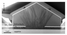
- Patent Documents 10 and 11 describe that ELO crystal growth is carried out using a PSS substrate to obtain a crystal film having a surface area of 9 ⁇ m 2 or more and a transition density of 5 ⁇ 10 6 cm- 2.
- gallium oxide has a problem in heat dissipation, and in order to solve the problem in heat dissipation, for example, it is necessary to reduce the thickness of gallium oxide to 30 ⁇ m or less, but the polishing process becomes complicated and the cost increases.
- the adhesion between the dielectric film and the semiconductor layer is not good.
- the series resistance in the case of a vertical device was not sufficiently satisfactory.
- Patent Documents 1 to 11 are publications relating to patents or patent applications by the applicants, and are still under study.
- One of the aspects of the semiconductor device of the present invention is to reduce the dislocation density of a semiconductor.
- one object of the present invention is to provide a semiconductor device including a semiconductor film in which the dislocation density of the Schottky junction region is smaller than the dislocation density of the ohmic junction region of the semiconductor film. ..
- the present inventor has carried out ELO (Epitaxial Lateral Overgrown) under specific conditions, so that the dislocation density of the Schottky junction region of the semiconductor film is determined by that of the semiconductor film. It has been found that a semiconductor device having a dislocation density smaller than that in the ohmic junction region can be obtained, and it has been found that such a semiconductor device has excellent semiconductor characteristics and can lead to a solution to the above-mentioned conventional problems. Details will be described together with the embodiments.
- a semiconductor film including a shotkey junction region and an ohmic junction region, a shotkey electrode arranged on the shotkey junction region of the semiconductor film, and an ohmic electrode arranged on the ohmic junction region.
- a semiconductor device comprising the above, wherein the dislocation density of the shotky junction region of the semiconductor film is smaller than the dislocation density of the ohmic contact region of the semiconductor film.
- the semiconductor film includes a first semiconductor layer including the Schottky junction region and a second semiconductor layer including the ohmic junction region.
- the second semiconductor layer is an n + type semiconductor layer.
- SBD Schottky barrier diode
- JBD junction barrier diode
- a semiconductor system including a semiconductor device, wherein the semiconductor device is the semiconductor device according to any one of [1] to [14].
- a method for manufacturing a semiconductor device which comprises arranging a mask on a crystal substrate with the c-axis direction of the crystal substrate as the longitudinal direction, and crystal growing a semiconductor film on the crystalline substrate on which the mask is arranged. ..
- a semiconductor device including arranging a mask on a crystal layer formed on a crystal substrate with the c-axis direction as a longitudinal direction, and crystal growing a semiconductor film on the crystal layer on which the mask is arranged. Manufacturing method. [18] The production method according to the above [16] or [17], wherein the mask contains an electrode material.
- the transposition density of the Schottky junction region of the semiconductor film is set to the ohmic junction region of the semiconductor film. It is smaller than the rearrangement density and has excellent semiconductor characteristics. Details will be described together with the embodiments.
- HVPE halide vapor deposition
- FIG. 1 It is a figure which shows typically an example of the semiconductor device bonded with a lead frame, a circuit board, or a heat dissipation board. It is a figure which shows an example of a power card schematically.
- the TEM image in the Example of this invention is shown.
- a main part of an example of a semiconductor device is shown.
- a main part of an example of a semiconductor device is shown.
- a cross-sectional view of a semiconductor device SBD
- JBS cross-sectional view of a semiconductor device
- FIG. 1 it is a schematic explanatory drawing which shows a part of the manufacturing process of a semiconductor device.
- FIG. 1 it is a schematic explanatory drawing which shows a part of the manufacturing process of a semiconductor device.
- FIG. 1 it is a schematic explanatory drawing which shows a part of the manufacturing process of a semiconductor device.
- FIG. 1 it is a schematic explanatory drawing which shows a part of the manufacturing process of a semiconductor device.
- FIG. 1 it is a schematic explanatory drawing which shows a part of the manufacturing process of a semiconductor device.
- a cross-sectional view of a laminated structure obtained from a manufacturing process of a semiconductor device is shown.
- a cross-sectional view is shown as an example of the semiconductor device obtained from the manufacturing process of the semiconductor device.
- the semiconductor device includes a semiconductor film including a shotkey junction region and an ohmic junction region, and a shotkey electrode arranged on the shotkey junction region of the semiconductor film. And an ohmic electrode arranged on the ohmic contact region, the dislocation density of the shotky junction region of the semiconductor film is smaller than the dislocation density of the ohmic contact region of the semiconductor film. According to the embodiment of the present invention, dislocations in the region where Schottky bonding is performed can be selectively reduced, so that a semiconductor device having excellent semiconductor characteristics can be obtained.
- the Schottky junction region refers to, for example, a region of the semiconductor film in which the distance from the interface between the semiconductor film and the Schottky electrode is within 100 nm.
- the ohmic contact region refers to, for example, a region of the semiconductor film in which the distance from the interface between the semiconductor film and the ohmic electrode is within 100 nm.
- the semiconductor film forms an ohmic contact between a first semiconductor layer forming a Schottky junction with the Schottky electrode and the ohmic electrode. It is preferable to have a layer. Further, in the embodiment of the present invention, it is preferable that the dislocation density of the first semiconductor layer is smaller than the dislocation density of the second semiconductor layer.
- the semiconductor device is a semiconductor device including at least an electrode and a semiconductor film, the semiconductor film has a crystal structure including a c-axis, and the electrode is in the c-axis direction.
- the electrode extends in the c-axis direction
- the longitudinal direction of the electrode is parallel to the c-axis direction of the semiconductor film, and an angle within 5 ° with respect to the c-axis direction. Includes the direction of the range.
- the shape of the electrodes is not particularly limited, but when the electrode shapes are arranged having lengths in two or more directions, the longitudinal direction means a longer direction.
- the c-axis direction of the crystalline substrate is set as the longitudinal direction on the m-plane of the crystalline substrate having the m-plane as the main surface.
- the mask can be made of an electrode material. Since the semiconductor layer ELO-grown from the crystalline substrate is formed by extending onto the mask, when the mask is used as an electrode, the crystallinity near the interface between the electrode and the semiconductor layer is improved. Further, when a mask is used as an electrode, a semiconductor device having a good bonding state between the ELO-grown semiconductor layer and the electrode can be obtained.
- the manufacturing method includes forming a semiconductor layer made of a crystal film by laterally growing on a crystal substrate having an ELO mask, and the ELO
- the mask is used as an electrode or a gate insulating film.
- the mask can be formed of a material containing Si, which is less conductive than the electrode.
- the mask may include a dielectric material or may be a mask made of a dielectric material. The mask may be used as a dielectric film in a semiconductor device.
- the semiconductor device is a semiconductor device including at least a dielectric film and a semiconductor film, and the semiconductor film has a crystal structure including a c-axis.
- the dielectric film is characterized in that it extends in the c-axis direction.
- “the dielectric film extends in the c-axis direction” means that the longitudinal direction of the dielectric film is parallel to the c-axis direction of the semiconductor film, with respect to the c-axis direction. Includes directions in an angular range within 5 °.
- the manufacturing method includes forming a semiconductor layer including lateral growth on a crystalline substrate on which a mask is arranged.
- a mask containing an electrode material can be placed on a crystalline substrate and used for ELO growth, and then the mask can be used as an electrode of a semiconductor device.
- a mask containing a dielectric material can be arranged, used for ELO growth, and then used as a gate insulating film of a semiconductor device.
- the phrase "the dielectric film extends in the c-axis direction” means that the longitudinal direction of the dielectric film is parallel to the c-axis direction of the semiconductor film, as described above. Includes directions in an angular range within 5 ° with respect to the direction. The entire longitudinal direction of the dielectric film may be parallel to the c-axis direction, or a part of the dielectric film may extend in the c-axis direction.
- the "c-axis direction” means a direction perpendicular to the c-plane in the present embodiment.
- the semiconductor device has a good bonding state at the interface between the dielectric film and the semiconductor layer, good crystallinity of the channel layer, and excellent semiconductor characteristics. Can be obtained.
- the semiconductor layer includes a lateral growth region.
- the semiconductor layer includes a first semiconductor region and a second semiconductor region, the first semiconductor region is bonded to the dielectric film, and the second semiconductor. It is preferable that the region contains more dislocations than the first semiconductor region. It is also preferable that the thickness of the semiconductor layer is 1 ⁇ m or more.
- the semiconductor layer has a corundum structure. It is also preferable that the semiconductor layer contains at least gallium. It is also preferable that the dielectric film is a gate insulating film. Further, as one of the embodiments of the present invention, the semiconductor device includes at least a dielectric film, a first semiconductor layer, and a second semiconductor layer, and the first semiconductor layer includes a c-axis. It is also preferable that the dielectric film has a crystal structure and extends in the c-axis direction. Further, the first semiconductor layer includes a first semiconductor region and a second semiconductor region, the second semiconductor layer includes a first semiconductor region and a second semiconductor region, and the first semiconductor layer is included.
- the first semiconductor region of the semiconductor layer is bonded to the dielectric film, and the first semiconductor region in the first semiconductor layer has fewer rearrangements than the second semiconductor region.
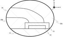
- the preferred semiconductor device described above include the semiconductor device shown in FIG. 11 or FIG. According to such a semiconductor device, a higher quality channel layer can be formed, and more excellent semiconductor characteristics can be exhibited. More specifically, FIG. 11 is a diagram showing a main part of the MOSFET, and the MOSFET of FIG. 11 includes a substrate 11, a gate electrode 14, a gate insulating film 15, a channel layer 18, an n-type semiconductor layer 18a, and It includes at least an n + type semiconductor layer 18b.
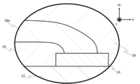
- FIG. 12 is a diagram showing a main part of the SBD, and the SBD of FIG. 12 includes at least a substrate 11, an electrode (Schottky electrode) 14, a semi-insulator layer 16, and an n-type semiconductor layer 18a.
- the Schottky electrode material for the ELO mask as the Schottky electrode, not only the Schottky junction is improved, but also preferably, for example, the drift layer near the Schottky interface is dislocated-free. It can be a layer and can exhibit more excellent semiconductor characteristics.
- the dielectric film (dielectric material) is not particularly limited, and may be a known dielectric film.
- the relative permittivity of the dielectric film is not particularly limited, but the relative permittivity is preferably 5 or less.
- the "relative permittivity" is the ratio of the permittivity of the film to the permittivity of the vacuum.
- the dielectric film include an oxide film, a phosphorylate film, a nitride film, and the like, but in the present invention, the dielectric film is preferably a film containing Si.
- a silicon oxide-based film is a preferable example.
- the silicon oxide-based film examples include a SiO 2 film, a phosphorus-added SiO 2 (PSG) film, a boron-added SiO 2 film, a phosphorus- boron-added SiO 2 film (BPSG film), a SiOC film, and a SiOF film.
- the means for forming the dielectric film is not particularly limited, and examples thereof include a CVD method, an atmospheric pressure CVD method, a plasma CVD method, a mist CVD method, and a thermal oxidation method. In the present invention, it is preferable that the means for forming the dielectric film is a mist CVD method or an atmospheric pressure CVD method.
- the film thickness of the dielectric film is also not particularly limited, but it is preferable that the film thickness of at least a part of the insulator film is 1 ⁇ m or more. According to the present invention, even when such a thick dielectric film is laminated on the semiconductor layer, a material having no crystal defects due to stress concentration in the semiconductor layer can be more preferably obtained. Further, the gate insulating film is not particularly limited as long as it does not interfere with the object of the present invention, and may be a known gate insulating film.
- the gate insulating film contains, for example, SiO 2 , Si 3 N 4 , Al 2 O 3 , GaO, AlGaO, InAlGaO, AlInZnGaO 4 , AlN, Hf 2 O 3 , SiN, SiON, MgO, GdO, and phosphorus.
- An oxide film such as an oxide film is a preferable example.
- the gate insulating film forming means may be a known means, and examples of such known forming means include a dry method and a wet method. Examples of the dry method include known means such as sputtering, vacuum deposition, CVD, and PLD. Examples of the wet method include application means such as screen printing and die coating.
- the semiconductor layer (hereinafter, also simply referred to as “oxide semiconductor film”, “semiconductor film”, or “crystal film”) is preferably an oxide having a corundum structure. Further, in the present invention, the oxide is one or two selected from Group 9 (eg, cobalt, rhodium, iridium, etc.) and Group 13 (eg, aluminum, gallium, indium, etc.) of the periodic table. It preferably contains the above metals, more preferably at least one metal selected from aluminum, indium, gallium and iridium, even more preferably at least gallium or iridium, and at least gallium. Most preferably.
- Group 9 eg, cobalt, rhodium, iridium, etc.
- Group 13 eg, aluminum, gallium, indium, etc.
- the main surface of the oxide semiconductor film is the m-plane because it can further suppress the diffusion of oxygen and the like and further improve the electrical characteristics.
- the oxide semiconductor film may have an off-angle.
- the oxide is ⁇ -Ga 2 O 3 or a mixed crystal thereof.
- the "main component" means that the oxide is contained in an atomic ratio of preferably 50% or more, more preferably 70% or more, still more preferably 90% or more with respect to all the components of the semiconductor layer. It means that it may be 100%.
- the thickness of the semiconductor layer is not particularly limited and may be 1 ⁇ m or less or 1 ⁇ m or more, but in the present invention, it is preferably 1 ⁇ m or more, and is preferably 10 ⁇ m or more. Is more preferable.
- the surface area of the semiconductor film is not particularly limited , but may be 1 mm 2 or more, 1 mm 2 or less, preferably 10 mm 2 to 300 cm 2 , and 100 mm 2 to 100 cm 2 . Is more preferable.
- the semiconductor film is preferably a single crystal film, but may be a polycrystalline film or a crystal film containing polycrystals.
- an n + type semiconductor layer is formed on a crystalline substrate, and the dopant concentration on the n + type semiconductor layer is reduced as compared with, for example, an n + type semiconductor layer.
- the n-type semiconductor layer can be formed to form a semiconductor film including at least a first semiconductor layer and a second semiconductor layer. Further, according to the embodiment of the present invention, since the growth direction of dislocations can be converged, the crystallinity of the region of the semiconductor film, which is particularly related to the characteristics of the semiconductor device (particularly the Schottky characteristics), is further increased. You can also do it.
- the semiconductor layer preferably contains a dopant.
- the dopant is not particularly limited and may be a known one. Examples of the dopant include n-type dopants such as tin, germanium, silicon, titanium, zirconium, vanadium and niobium, and p-type dopants such as magnesium, calcium and zinc.
- the semiconductor layer preferably contains an n-type dopant, and more preferably an n-type oxide semiconductor layer. Further, in the present invention, the n-type dopant is preferably Sn, Ge or Si.
- the content of the dopant is preferably 0.00001 atomic% or more, more preferably 0.00001 atomic% to 20 atomic%, and 0.00001 atomic% to 10 atomic% in the composition of the semiconductor layer. Is most preferable. More specifically, the concentration of the dopant may usually be about 1 ⁇ 10 16 / cm 3 to 1 ⁇ 10 22 / cm 3 , and the concentration of the dopant may be, for example, about 1 ⁇ 10 17 / cm. The concentration may be as low as 3 or less. Further, according to one aspect of the present invention, the dopant may be contained in a high concentration of about 1 ⁇ 10 20 / cm 3 or more.
- the concentration of the fixed charge of the semiconductor layer is also not particularly limited, but one of the embodiments of the semiconductor device of the present invention is that the concentration of the fixed charge is 1 ⁇ 10 17 / cm 3 or less, which is better than the depletion layer. Is preferable because it can form.
- the semiconductor layer may be formed by using known means.
- the means for forming the semiconductor layer include a CVD method, a MOCVD method, a MOVPE method, a mist CVD method, a mist epitaxy method, an MBE method, an HVPE method, a pulse growth method, and an ALD method.
- the semiconductor layer hereinafter, also referred to as “crystal growth layer” or “crystal film”.
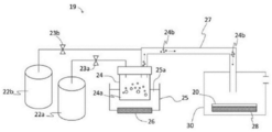
- the HVPE apparatus shown in FIG. 2 is used to gasify a metal source containing a metal into a metal-containing raw material gas, and then the metal-containing raw material gas and an oxygen-containing raw material.
- a metal source containing a metal into a metal-containing raw material gas
- the metal-containing raw material gas and an oxygen-containing raw material are supplied onto a crystalline substrate in the reaction chamber to form a film
- a crystalline substrate containing, for example, an ELO mask made of the dielectric film is used on the surface, and the reactive gas is subjected to the crystalline substrate.
- the film may be supplied onto a substrate and the film formation may be carried out under the flow of the reactive gas.
- the crystalline substrate is preferably a crystalline substrate.
- the crystalline substrate may include a crystalline substrate and a crystal layer arranged on the crystalline substrate.
- the metal source is not particularly limited as long as it contains a metal and can be gasified, and may be a simple substance of a metal or a metal compound.
- the metal include one or more metals selected from gallium, aluminum, indium, iron, chromium, vanadium, titanium, rhodium, nickel, cobalt, iridium and the like.
- the metal is preferably one or more metals selected from gallium, aluminum and indium, more preferably gallium, and the metal source is gallium alone. Most preferred.
- the metal source may be a gas, a liquid, or a solid, but in the present invention, for example, when gallium is used as the metal, the metal is used.
- the source is preferably a liquid.
- the gasification means is not particularly limited and may be a known means as long as the object of the present invention is not impaired.
- the gasification means is preferably carried out by halogenating the metal source.
- the halogenating agent used for the halogenation is not particularly limited as long as the metal source can be halogenated, and may be a known halogenating agent.
- the halogenating agent include halogens and hydrogen halides.
- the halogen include fluorine, chlorine, bromine, iodine and the like.
- the hydrogen halide include hydrogen fluoride, hydrogen chloride, hydrogen bromide, hydrogen iodide and the like.
- hydrogen halide is preferably used for the halogenation, and hydrogen chloride is more preferably used.
- the gasification is carried out by supplying halogen or hydrogen halide as a halogenating agent to the metal source and reacting the metal source with halogen or hydrogen halide at a temperature equal to or higher than the vaporization temperature of the metal halide. It is preferable to carry out the process by forming a metal halide.
- the halogenation reaction temperature is not particularly limited, but in the present invention, for example, when the metal of the metal source is gallium and the halogenating agent is HCl, it is preferably 900 ° C. or lower, preferably 700 ° C.
- the temperature is most preferably 400 ° C. to 700 ° C.
- the metal-containing raw material gas is not particularly limited as long as it is a gas containing the metal of the metal source.
- the metal-containing raw material gas include halides (fluoride, chloride, bromide, iodide, etc.) of the metal.
- the metal-containing raw material gas and the oxygen-containing raw material gas are placed on a crystalline substrate in the reaction chamber. Supply. Further, in the embodiment of the present invention, the reactive gas is supplied onto the substrate.
- the oxygen-containing raw material gas include O 2 gas, CO 2 gas, NO gas, NO 2 gas, N 2 O gas, H 2 O gas, O 3 gas and the like.
- the oxygen-containing raw material gas may contain CO 2.
- the reactive gas is usually a reactive gas different from the metal-containing raw material gas and the oxygen-containing raw material gas, and does not contain an inert gas.
- the reactive gas is not particularly limited, and examples thereof include an etching gas and the like.
- the etching gas is not particularly limited and may be a known etching gas as long as the object of the present invention is not impaired.
- the reactive gas is a halogen gas (for example, fluorine gas, chlorine gas, bromine gas, iodine gas, etc.), hydrogen halide gas (for example, hydrofluoric acid gas, hydrochloric acid gas, hydrogen bromide gas, hydrogen bromide gas, iodine gas, etc.).
- the metal-containing raw material gas, the oxygen-containing raw material gas, and the reactive gas may contain a carrier gas.
- the carrier gas include an inert gas such as nitrogen and argon.
- the partial pressure of the metal-containing raw material gas is not particularly limited, but in the present invention, it is preferably 0.5 Pa to 1 kPa, and more preferably 5 Pa to 0.5 kPa.
- the partial pressure of the oxygen-containing raw material gas is not particularly limited, but in the present invention, it is preferably 0.5 to 100 times the partial pressure of the metal-containing raw material gas, and is 1 to 20 times. Is more preferable.
- the partial pressure of the reactive gas is also not particularly limited, but in the embodiment of the present invention, it is preferably 0.1 to 5 times the partial pressure of the metal-containing raw material gas, and 0.2 to 3 times. It is more preferable to double.
- the dopant-containing raw material gas is not particularly limited as long as it contains a dopant.
- the dopant is also not particularly limited, but in the present invention, the dopant preferably contains one or more elements selected from germanium, silicon, titanium, zirconium, vanadium, niobium and tin, preferably germanium. It is more preferably containing silicon or tin, and most preferably it contains germanium.
- the dopant-containing raw material gas preferably has the dopant in the form of a compound (for example, a halide, an oxide, etc.), and more preferably in the form of a halide.
- the partial pressure of the dopant-containing raw material gas is not particularly limited, but in the present invention, it is preferably 1 ⁇ 10 -7 times to 0.1 times the partial pressure of the metal-containing raw material gas, and is 2.5 ⁇ . More preferably, it is 10-6 times to 7.5 ⁇ 10-2 times. In the present invention, it is preferable to supply the dopant-containing raw material gas together with the reactive gas onto the crystalline substrate.
- the crystalline substrate is a crystalline substrate.
- the crystal substrate is not particularly limited as long as it is a substrate containing a crystal as a main component, and may be a known substrate. It may be an insulator substrate, a conductive substrate, or a semiconductor substrate. It may be a single crystal substrate or a polycrystalline substrate. Examples of the crystal substrate include a substrate containing a crystal having a corundum structure as a main component.
- the "main component" refers to a composition ratio in the substrate containing 50% or more of the crystals, preferably 70% or more, and more preferably 90% or more.
- Examples of the substrate containing the crystal having a corundum structure as a main component include a sapphire substrate and an ⁇ -type gallium oxide substrate.
- the crystal substrate is preferably a sapphire substrate.
- the sapphire substrate include an m-plane sapphire substrate and an a-plane sapphire substrate.
- the sapphire substrate is preferably an m-plane sapphire substrate.
- the sapphire substrate may have an off angle. The off angle is not particularly limited, but is preferably 0 ° to 15 °.
- the thickness of the crystal substrate is not particularly limited, but is preferably 50 to 2000 ⁇ m, and more preferably 200 to 800 ⁇ m.
- the area of the crystal substrate is not particularly limited , but is preferably 15 cm 2 or more, and more preferably 100 cm 2 or more.
- the crystalline substrate includes, for example, a mask made of the electrodes (also referred to as an ELO mask).
- the constituent material of the ELO mask is not particularly limited, but is preferably an electrode material. Further, the constituent material has conductivity, and it is preferable to use it as an ohmic electrode and a Schottky electrode, respectively.
- the electrode material may be a known metal. Preferred examples of the metal include at least one metal selected from the 4th to 11th groups of the periodic table. Examples of the metal of Group 4 of the periodic table include titanium (Ti), zirconium (Zr), and hafnium (Hf).
- Examples of the metal of Group 5 of the periodic table include vanadium (V), niobium (Nb), and tantalum (Ta).
- Examples of the metal of Group 6 of the periodic table include chromium (Cr), molybdenum (Mo) and tungsten (W).
- Examples of the metal of Group 7 of the periodic table include manganese (Mn), technetium (Tc), and rhenium (Re).
- Examples of the metal of Group 8 of the periodic table include iron (Fe), ruthenium (Ru), and osmium (Os).
- Examples of the metal of Group 9 of the periodic table include cobalt (Co), rhodium (Rh), and iridium (Ir).
- Examples of the metal of Group 10 of the periodic table include nickel (Ni), palladium (Pd), platinum (Pt) and the like.
- Examples of the metal of Group 11 of the periodic table include copper (Cu), silver (Ag), and gold (Au).
- the layer thickness of each of the metal layers is not particularly limited, but is preferably 0.1 nm to 10 ⁇ m, more preferably 5 nm to 500 nm, and most preferably 10 nm to 200 nm.
- the electrode forming means is not particularly limited and may be a known means. Specific examples of the forming means include a dry method and a wet method. Examples of the dry method include sputtering, vacuum deposition, and CVD. Examples of the wet method include screen printing and die coating.
- the crystalline substrate contains an ELO mask made of, for example, the dielectric film (for example, a gate insulating film).
- the ELO mask usually includes a gate electrode.
- the electrode material of the gate electrode include the following electrode materials.
- the constituent material of the convex portion examples include oxides such as Si, Ge, Ti, Zr, Hf, Ta, Sn, nitrides or carbides, carbon, diamond, metal, and mixtures thereof. More specifically, a Si-containing compound containing SiO 2 , SiN or polycrystalline silicon as a main component, and a metal having a melting point higher than the crystal growth temperature of the crystalline oxide semiconductor (for example, platinum, gold, silver, palladium). , Rhodium, iridium, precious metals such as ruthenium, etc.).
- the content of the constituent material is preferably 50% or more, more preferably 70% or more, and most preferably 90% or more in the convex portion in terms of composition ratio.
- the ELO mask forming means may be a known means, for example, a known patterning processing means such as photolithography, electron beam lithography, laser patterning, and subsequent etching (for example, dry etching or wet etching). Can be mentioned.
- the pitch interval of the pattern shape is also not particularly limited, but in the embodiment of the present invention, it is preferably 100 ⁇ m or less, more preferably 0.5 ⁇ m to 50 ⁇ m, and 0.5 ⁇ m to 10 ⁇ m. Is the most preferable.
- crystal growth substrate crystal substrate
- FIG. 3 shows one aspect of the convex portion made of the ELO mask provided on the crystal growth surface of the crystal substrate preferably used in the present invention.
- the crystal substrate containing the ELO mask of FIG. 3 is formed of a crystal substrate 1 and a convex mask 2a on the crystal growth surface 1a.
- the mask 2a is striped with respect to the crystal growth surface 1a and extends in the c-axis direction. Striped convex portions 2a are periodically arranged on the crystal growth surface 1a of the crystal substrate 1.
- the convex portion 2a is made of, for example, a silicon-containing compound such as SiO 2 , and can be formed by using a known means such as photolithography.
- the metal layer 2 can be arranged as an ELO mask.
- the width, height, spacing, and the like of the convex portions are not particularly limited, but in the present invention, each is in the range of, for example, about 10 nm to about 1 mm, preferably about 10 nm to about 300 ⁇ m, and more preferably about. It is 10 nm to about 10 ⁇ m.
- the crystalline substrate 110 is a crystal substrate 1 and a crystal layer 3 (for example, a stress relaxation layer or the like) arranged on the crystal substrate 1.
- a buffer layer containing) may be included.
- the crystal substrate 1 has the buffer layer 3 arranged on at least a part of the surface of the crystal substrate.
- the ELO mask 2 is arranged in at least a part of the buffer layer 3.
- the crystalline substrate may have a buffer layer in which an ELO mask is placed on at least a part of the crystal substrate and epitaxially grown from the crystal substrate.
- the means for forming the buffer layer is not particularly limited and may be a known means.
- Examples of the forming means include a spray method, a mist CVD method, an HVPE method, an MBE method, a MOCVD method, a sputtering method and the like.
- a spray method a mist CVD method, an HVPE method, an MBE method, a MOCVD method, a sputtering method and the like.
- the buffer layer is preferably used, for example, by atomizing or dropletizing the raw material solution using the mist CVD apparatus shown in FIG. 4 (atomization step), and using a carrier gas to atomize the obtained atomized droplets. It can be formed by transporting to the substrate (conveying step) and then thermally reacting the atomized droplets on a part or all of the surface of the substrate (buffer layer forming step). In the present invention, the crystal growth layer can be formed in the same manner.
- the atomization step atomizes the raw material solution to obtain the atomized droplets.
- the means for atomizing the raw material solution is not particularly limited as long as the raw material solution can be atomized, and may be known means. However, in the embodiment of the present invention, the means for atomizing the raw material solution using ultrasonic waves is used. preferable. Atomized droplets obtained using ultrasonic waves have a zero initial velocity and are preferable because they float in the air. For example, instead of spraying them like a spray, they float in space and are transported as a gas. Since it is a possible mist, it is not damaged by collision energy, so it is very suitable.
- the droplet size of the atomized droplet is not particularly limited and may be a droplet of about several mm, but is preferably 50 ⁇ m or less, and more preferably 0.1 to 10 ⁇ m.
- the raw material solution is not particularly limited as long as it can be atomized and the buffer layer can be obtained by mist CVD.
- the raw material solution include an aqueous solution of an organic metal complex of an atomizing metal (for example, an acetylacetonate complex) and a halide (for example, fluoride, chloride, bromide, iodide, etc.).
- the atomizing metal is not particularly limited, and such atomizing metal is selected from, for example, aluminum, gallium, indium, iron, chromium, vanadium, titanium, rhodium, nickel, cobalt, iridium and the like1 Species or two or more kinds of metals and the like can be mentioned.
- the atomizing metal preferably contains at least gallium, indium or aluminum, and more preferably at least gallium.
- the content of the atomizing metal in the raw material solution is not particularly limited as long as the object of the present invention is not impaired, but is preferably 0.001 mol% to 50 mol%, and more preferably 0.01 mol% to. It is 50 mol%.
- the raw material solution contains a dopant.
- the dopant is preferably tin, germanium, or silicon, more preferably tin, or germanium, and most preferably tin.
- the concentration of the dopant may be usually about 1 ⁇ 10 16 / cm 3 to 1 ⁇ 10 22 / cm 3 , and the concentration of the dopant is, for example, a low concentration of about 1 ⁇ 10 17 / cm 3 or less.
- the dopant may be contained in a high concentration of about 1 ⁇ 10 20 / cm 3 or more.
- the solvent of the raw material solution is not particularly limited, and may be an inorganic solvent such as water, an organic solvent such as alcohol, or a mixed solvent of an inorganic solvent and an organic solvent.
- the solvent preferably contains water, more preferably water or a mixed solvent of water and alcohol, and most preferably water. More specific examples of the water include pure water, ultrapure water, tap water, well water, mineral spring water, mineral water, hot spring water, spring water, fresh water, seawater, and the like. Ultrapure water is preferred.
- the atomized droplets are conveyed into the film forming chamber by using a carrier gas.
- the carrier gas is not particularly limited as long as the object of the present invention is not impaired, and examples thereof include an inert gas such as oxygen, ozone, nitrogen and argon, and a reducing gas such as hydrogen gas and forming gas. ..
- the type of the carrier gas may be one type, but may be two or more types, and a diluted gas having a reduced flow rate (for example, a 10-fold diluted gas) or the like is further used as the second carrier gas. May be good.
- the carrier gas may be supplied not only at one location but also at two or more locations.
- the flow rate of the carrier gas is not particularly limited, but is preferably 0.01 to 20 L / min, and more preferably 1 to 10 L / min.
- the flow rate of the diluting gas is preferably 0.001 to 2 L / min, more preferably 0.1 to 1 L / min.
- the buffer layer is formed on the crystal substrate by thermally reacting the atomized droplets in the film forming chamber.
- the thermal reaction may be such that the atomized droplets react with heat, and the reaction conditions and the like are not particularly limited as long as the object of the present invention is not impaired.
- the thermal reaction is usually carried out at a temperature equal to or higher than the evaporation temperature of the solvent, but is preferably not too high (for example, 1000 ° C.) or lower, more preferably 650 ° C. or lower, and most preferably 400 ° C. to 650 ° C. preferable.
- the thermal reaction may be carried out under any atmosphere of vacuum, non-oxygen atmosphere, reducing gas atmosphere and oxygen atmosphere as long as the object of the present invention is not impaired, and the thermal reaction may be carried out under atmospheric pressure or pressure. It may be carried out under either reduced pressure or reduced pressure, but in the present invention, it is preferably carried out under atmospheric pressure.
- the thickness of the buffer layer can be set by adjusting the formation time.
- the buffer layer After forming the buffer layer as described above, by arranging a mask layer on the buffer layer by the above method to form the crystal growth layer, defects such as tilt in the crystal growth layer can be further improved. It can be reduced and the film quality can be improved.
- the buffer layer is not particularly limited, but in the present invention, it is preferable that the buffer layer contains a metal oxide as a main component.
- the metal oxide include metal oxides containing one or more metals selected from aluminum, gallium, indium, iron, chromium, vanadium, titanium, rhodium, nickel, cobalt, iridium and the like. Be done.
- the metal oxide preferably contains one or more elements selected from indium, aluminum and gallium, more preferably at least indium and / and gallium, and at least gallium. Is most preferable to contain.
- the buffer layer may contain a metal oxide as a main component, and the metal oxide contained in the buffer layer may contain gallium and a smaller amount of aluminum than gallium. ..
- the buffer layer may include a superlattice structure. By using the buffer layer including the superlattice structure, not only good crystal growth can be realized, but also warpage during crystal growth can be suppressed more easily.
- the "main component” is preferably 50% or more, more preferably 70% or more, still more preferably 90% or more of the metal oxide in terms of atomic ratio with respect to all the components of the buffer layer. It means that it is included, and it means that it may be 100%.
- the crystal structure of the crystalline oxide semiconductor is not particularly limited, but in the present invention, a corundum structure is preferable.
- the first lateral crystal growth layer and the buffer layer may have the same main components or different main components from each other as long as the object of the present invention is not impaired, but in the present invention. Are preferably the same.
- a metal-containing raw material gas, an oxygen-containing raw material gas, a reactive gas and, if desired, a dopant-containing raw material gas are supplied onto the substrate on which the buffer layer may be provided, and the reactive gas is supplied.
- the film is formed under the distribution of.
- it is preferable that the film formation is performed on a heated substrate.
- the film formation temperature is not particularly limited as long as the object of the present invention is not impaired, but is preferably 900 ° C. or lower, more preferably 700 ° C. or lower, and most preferably 400 ° C. to 700 ° C.
- the film formation may be carried out under any of vacuum, non-vacuum, reducing gas atmosphere, inert gas atmosphere and oxidizing gas atmosphere as long as the object of the present invention is not impaired. Further, it may be carried out under normal pressure, atmospheric pressure, pressurization or reduced pressure, but in the above-described embodiment of the present invention, it is preferably carried out under normal pressure or atmospheric pressure.
- the film thickness can be set by adjusting the film formation time.
- the crystal growth layer usually contains a crystalline metal oxide as a main component.
- the crystalline metal oxide include metal oxides containing one or more metals selected from aluminum, gallium, indium, iron, chromium, vanadium, titanium, rhodium, nickel, cobalt, iridium and the like. Can be mentioned.
- the crystalline metal oxide preferably contains one or more elements selected from indium, aluminum and gallium, more preferably at least indium and / and gallium. , Crystalline gallium oxide or a mixed crystal thereof is most preferable.
- the "main component" is preferably 50 in terms of atomic ratio of the crystalline metal oxide with respect to all the components of the first lateral crystal growth layer.
- a crystal growth film having a corundum structure can be obtained by performing the film formation using a substrate containing a corundum structure as the substrate.
- the crystalline metal oxide may be a single crystal or a polycrystal, but in the embodiment of the present invention, it is preferably a single crystal.
- the upper limit of the thickness of the first lateral crystal growth layer is not particularly limited, but is, for example, 100 ⁇ m, and the lower limit of the thickness of the crystal growth layer is not particularly limited, but is preferably 1 ⁇ m, and is preferably 10 ⁇ m.
- the thickness of the first lateral crystal growth layer is preferably 3 ⁇ m to 100 ⁇ m, more preferably 10 ⁇ m to 100 ⁇ m, and most preferably 20 ⁇ m to 100 ⁇ m.
- FIGS. 1 (a) to 1 (c) it is preferable to use a sapphire substrate as a crystalline substrate as shown in FIGS. 1 (a) to 1 (c).
- a sapphire substrate having the m-plane or the a-plane as the main surface as the sapphire substrate.
- FIG. 1A shows the sapphire substrate 1. As shown in FIG.
- the ELO mask 5 is formed on the crystal growth surface of the sapphire substrate 1.
- the ELO mask 5 is arranged with the c-axis direction as the longitudinal direction and has a stripe shape with respect to the crystal growth plane.
- a crystal growth layer is formed using the crystal growth substrate of FIG. 1 (b), and the laminated structure of FIG. 1 (c) is obtained.
- the crystal growth layer 8 is formed on the sapphire substrate 1 having the ELO mask 5 as an electrode on the surface, and the region near the interface in contact with the electrode is, for example, dislocation-free. It is a region and can exhibit excellent semiconductor characteristics.
- after the mask 5 is used for forming the crystal growth layer 8 it can be used as an electrode (for example, an ohmic electrode) of a semiconductor device.
- FIGS. 15-a to 16-b will be described.
- the crystalline substrate 110 has a crystal substrate 1 and a crystal layer 3 arranged on the crystal substrate.
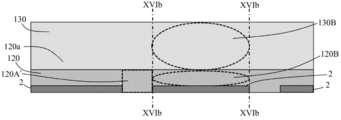
- the laminated structure shown in FIG. 15-a is obtained by crystal-growing the first crystal growth layer 120 on the crystal substrate 1 having the crystal layer 3 and the mask layer (ELO mask) 2 on the surface.
- ELO mask mask layer
- an m-plane sapphire substrate is used as the crystal substrate 1
- ⁇ -Ga 2 O 3 is used as the crystal layer 3 (buffer layer).
- mask layers 2 having the c-axis direction as the longitudinal direction are arranged on the upper surface of the crystalline substrate 110 (crystal growth surface, in this case, the upper surface of the buffer layer) at regular intervals, and the first crystal is formed.
- the growth layer 120 is formed.
- dislocations grow in the m-axis direction from the upper surface of the crystalline substrate, and the dislocations that start to grow in the m-axis direction in FIG. 15-a are bent in the a-axis direction.
- the dislocations can be converged. Since the crystal grows laterally on the mask layer 2, the dislocation density of the crystal growth region 120B is lower than the dislocation density of the crystal growth region 120A.
- the upper surface 120a of the first crystal growth layer 120 is made flat by polishing or the like. As a result, a part of the crystal growth region 120A having a high dislocation density converged in the a-axis direction is removed.
- the crystal is continuously grown on the flat upper surface 120a of the first crystal growth layer 120 to form the second crystal growth layer 130, and FIG. 15-b. Obtain a laminated structure of.
- the crystal region 120B of the first crystal growth layer 120 located on the mask layer 2 is a good crystal region having a low dislocation density including ELO growth, and a region having a high dislocation density converged in a certain direction is removed.
- the dislocation density of the crystal growth region 130B of the second growth layer 130 located above the mask layer 2 is lower than the dislocation density of the crystal growth region 120B of the first growth layer 120 located on the mask layer 2. can do.
- the crystalline substrate 110 can be removed.
- the crystalline substrate may be a crystal substrate, or may include a crystal substrate and a crystal layer (which may be a plurality of layers) arranged on the crystal substrate.
- at least the crystalline substrate is removed.
- the crystal substrate and the crystal layer arranged on the crystal substrate may be removed.
- the material of the mask layer 2 if it is not necessary to be included in the completed semiconductor device, not only the crystalline substrate but also the mask may be removed as shown in FIG. 17-a. Further, as shown in FIG.
- a crystal film formed in a large area is converted into a semiconductor device.
- a plurality of laminated structures including a semiconductor film and electrodes arranged on the semiconductor film can be obtained.
- a method in which a large area is formed and dicing may be performed vertically and horizontally, or a crystal film having a required area is individually formed and dicing for separation is not performed. You may take.
- an n + type ⁇ -Ga 2 O 3 layer is crystal-grown on the crystalline substrate 11 on which the mask layer 2 is arranged as described above, for example, as the first crystal growth layer 120.
- the dopant concentration was made lower than that when the first crystal growth layer 120 was formed, and the n-type ⁇ -Ga 2 was formed.
- the mask 2 containing the electrode material is an ohmic electrode
- a laminated structure including a semiconductor film including an ohmic contact region and an ohmic electrode arranged on the ohmic contact region as shown in FIG. 16-b can be formed.
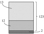
- the semiconductor film includes an n-type ⁇ -Ga 2 O 3 layer as the first semiconductor layer 13 and an n + type ⁇ -Ga 2 O 3 layer as the second semiconductor layer 12.
- a Schottky electrode is formed on the first semiconductor layer 13 by using, for example, a known electrode forming different method, using a mask arranged in contact with the second semiconductor layer 12 as an ohmic electrode. You can also do it.
- the electrodes By forming the electrodes in this way, the adhesion between the electrodes and the semiconductor film can be improved, and the semiconductor device 100 as shown in FIG. 13 can be obtained.
- the semiconductor device 100 shown in FIG. 13 is, for example, an SBD in which a semiconductor film 123 including a Schottky junction region 13B and an ohmic contact region 12B and a shot arranged on the Schottky junction region 13B of the semiconductor film 123. It includes a key electrode 32 and an ohmic electrode 35 arranged on the ohmic contact region 12B.
- the dislocation density of the Schottky junction region 13B of the semiconductor film 123 is smaller than the dislocation density of the ohmic junction region 12B of the semiconductor film 123, and a region having good crystallinity is formed. It can be a Schottky junction area.
- the Schottky junction region 13B refers to, for example, a region of the semiconductor film 123 in which the distance from the interface between the semiconductor film 123 and the Schottky electrode 32 is within 100 nm.
- the ohmic contact region 13B refers to, for example, a region of the semiconductor film 123 in which the distance from the interface between the semiconductor film 123 and the ohmic electrode 35 is within 100 nm.
- the semiconductor film 123 forms an ohmic contact between the first semiconductor layer 13 that forms a Schottky bond with the Schottky electrode 32 and the ohmic electrode 35. It is preferable to have the second semiconductor layer 12. Further, in the embodiment of the present invention, it is preferable that the dislocation density of the first semiconductor layer 13 is smaller than the dislocation density of the second semiconductor layer 12.
- the semiconductor device 200 shown in FIG. 14 is, for example, a JBS shot arranged on the Schottky junction region 13B of the semiconductor film 123 and the semiconductor film 123 including the Schottky junction region 13B and the ohmic contact region 12B. It includes a key electrode 32 and an ohmic electrode 2 arranged on the ohmic contact region 12B.
- a plurality of trenches 36 are formed in the Schottky junction region of the first semiconductor layer 13. It can be formed by burying a p-type semiconductor region 33 in the trench 36 as one of the embodiments of JBS.
- the trench 36 can be formed by selectively etching the first semiconductor layer 13 by, for example, etching, and may be performed by etching by a mist CVD method.
- a p-type semiconductor region may be formed in the trench by using a mist CVD method.
- JBS it is also possible to form a dielectric layer in the trench 36 and embed a semiconductor region in the trench via the dielectric layer.
- a region having good crystallinity can be a Schottky junction region.
- a semiconductor device having good semiconductor characteristics can be obtained by arranging p-type semiconductor regions embedded in a plurality of trenches in the Schottky junction region.
- the ELO mask may include an electrode material.
- the electrode material include metal oxidation of metals or alloys of two or more of the metals, tin oxide, zinc oxide, renium oxide, indium oxide, indium tin oxide (ITO), indium zinc oxide (IZO), and the like.
- examples thereof include a conductive material, an organic conductive compound such as polyaniline, polythiophene or polypyrrole, or a mixture thereof, but in the present invention, a metal is preferable.
- Preferred examples of the metal include at least one metal selected from Groups 4 to 10 of the Periodic Table.
- Examples of the metal of Group 4 of the periodic table include titanium (Ti), zirconium (Zr), and hafnium (Hf).
- Examples of the metal of Group 5 of the periodic table include vanadium (V), niobium (Nb), and tantalum (Ta).
- Examples of the metal of Group 6 of the periodic table include chromium (Cr), molybdenum (Mo) and tungsten (W).
- Examples of the metal of Group 7 of the periodic table include manganese (Mn), technetium (Tc), and rhenium (Re).
- Examples of the metal of Group 8 of the periodic table include iron (Fe), ruthenium (Ru), and osmium (Os).
- Examples of the metal of Group 9 of the periodic table include cobalt (Co), rhodium (Rh), and iridium (Ir).
- Examples of the metal of Group 10 of the periodic table include nickel (Ni), palladium (Pd), platinum (Pt) and the like.
- the method of forming the electrode is not particularly limited, and is a wet method such as a printing method, a spray method, a coating method, a physical method such as a vacuum deposition method, a sputtering method, and an ion plating method, a CVD method, and a plasma CVD method. It can be formed on the crystalline substrate according to a method appropriately selected in consideration of suitability with the material from among chemical methods such as the above.
- the ELO mask includes a gate electrode.
- a gate electrode By covering the gate electrode with the ELO mask as a gate insulating film, an excellent semiconductor device, particularly MOSFET, can be easily obtained.
- the laminated structure can be particularly suitably used for a semiconductor device including at least an electrode and a semiconductor layer, and is particularly useful for a power device.
- the semiconductor device include transistors and TFTs such as SBDs, MOSFETs, MISs and HEMTs, Schottky barrier diodes using semiconductor-metal junctions, PN or PIN diodes combined with other P layers, and light emitting and receiving elements.
- the semiconductor device is suitably used as a semiconductor device by joining to a lead frame, a circuit board, a heat radiating board, or the like with a joining member based on a conventional method. It is suitably used as a power module, an inverter or a converter, and further, for example, a semiconductor system using a power supply device or the like.
- FIG. 8 shows a suitable example of the semiconductor device bonded to the lead frame, the circuit board, or the heat radiating board.
- both sides of the semiconductor element 500 are bonded to the lead frame, the circuit board, or the heat radiating board 502 by solder 501, respectively. With this configuration, a semiconductor device having excellent heat dissipation can be obtained.
- the periphery of the joining member such as solder is sealed with a resin.
- the power supply device can be manufactured from the semiconductor device or as a power supply device including the semiconductor device by connecting to a wiring pattern or the like by using a known method.
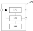
- the power supply system 170 is configured by using the plurality of power supply devices 171 and 172 and the control circuit 173.
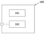
- the power supply system can be used in the system apparatus 180 by combining the electronic circuit 181 and the power supply system 182.
- FIG. 7 shows a power supply circuit of a power supply device including a power circuit and a control circuit.
- the DC voltage is switched at a high frequency by an inverter 192 (composed of MOSFETs A to D), converted to AC, and then insulated and transformed by a transformer 193. After rectifying with the rectifying MOSFET 194, smoothing with DCL195 (smoothing coils L1 and L2) and a capacitor, and outputting a DC voltage.
- the voltage comparator 197 compares the output voltage with the reference voltage, and the PWM control circuit 196 controls the inverter 192 and the rectifier MOSFET 194 so as to obtain a desired output voltage.
- the semiconductor device is preferably a power card, includes a cooler and an insulating member, and the coolers are provided on both sides of the semiconductor layer, respectively, via at least the insulating member. It is more preferable that heat radiating layers are provided on both sides of the semiconductor layer, and that the cooler is provided on the outside of the heat radiating layer at least via the insulating member.
- FIG. 9 shows a power card which is one of the preferred embodiments of the present invention. The power card of FIG.
- a double-sided cooling type power card 201 which includes a refrigerant tube 202, a spacer 203, an insulating plate (insulating spacer) 208, a sealing resin portion 209, a semiconductor chip 301a, and a metal heat transfer plate (protruding terminal). Section) 302b, a heat sink and an electrode 303, a metal heat transfer plate (protruding terminal section) 303b, a solder layer 304, a control electrode terminal 305, and a bonding wire 308.
- the cross section in the thickness direction of the refrigerant tube 202 has a large number of flow paths 222 partitioned by a large number of partition walls 221 extending in the flow path direction at predetermined intervals from each other. According to such a suitable power card, higher heat dissipation can be realized and higher reliability can be satisfied.
- the semiconductor chip 301a is joined by a solder layer 304 on the inner main surface of the metal heat transfer plate 302b, and the metal heat transfer plate (protruding terminal portion) 302b is formed by the solder layer 304 on the remaining main surface of the semiconductor chip 301a. It is joined so that the anode electrode surface and the cathode electrode surface of the flywheel diode are connected to the collector electrode surface and the emitter electrode surface of the IGBT in so-called antiparallel.
- Examples of the materials of the metal heat transfer plates (protruding terminal portions) 302b and 303b include Mo and W.
- the metal heat transfer plates (protruding terminal portions) 302b and 303b have a difference in thickness that absorbs the difference in thickness of the semiconductor chip 301a, whereby the outer surfaces of the metal heat transfer plates 302b and 303b are flat. ..
- the resin sealing portion 209 is made of, for example, an epoxy resin, and is molded by covering the side surfaces of the metal heat transfer plates 302b and 303b, and the semiconductor chip 301a is molded by the resin sealing portion 209. However, the outer main surface, that is, the contact heat receiving surface of the metal heat transfer plates 302b and 303b is completely exposed.
- the metal heat transfer plates (protruding terminal portions) 302b and 303b project to the right in FIG. 9 from the resin sealing portion 209, and the control electrode terminal 305, which is a so-called lead frame terminal, is, for example, a semiconductor chip 301a on which an IGBT is formed.
- the gate (control) electrode surface and the control electrode terminal 305 are connected.
- the insulating plate 208 which is an insulating spacer, is made of, for example, an aluminum nitride film, but may be another insulating film.
- the insulating plate 208 completely covers and adheres to the metal heat transfer plates 302b and 303b, but the insulating plate 208 and the metal heat transfer plates 302b and 303b may simply come into contact with each other or have good heat such as silicon grease. Heat transfer materials may be applied or they may be joined in various ways. Further, the insulating layer may be formed by ceramic spraying or the like, the insulating plate 208 may be bonded on the metal heat transfer plate, or may be bonded or formed on the refrigerant tube.
- the refrigerant tube 202 is manufactured by cutting an aluminum alloy into a plate material formed by a pultrusion molding method or an extrusion molding method to a required length.
- the cross section in the thickness direction of the refrigerant tube 202 has a large number of flow paths 222 partitioned by a large number of partition walls 221 extending in the flow path direction at predetermined intervals from each other.
- the spacer 203 may be, for example, a soft metal plate such as a solder alloy, or may be a film (film) formed by coating or the like on the contact surfaces of the metal heat transfer plates 302b and 303b.
- the surface of the soft spacer 203 is easily deformed to adapt to the minute irregularities and warpage of the insulating plate 208 and the minute irregularities and warpage of the refrigerant tube 202 to reduce the thermal resistance.
- a known good thermal conductive grease or the like may be applied to the surface of the spacer 203 or the like, or the spacer 203 may be omitted.
- Example 1 Fabrication of Semiconductor Device
- a crystal growth substrate a crystalline substrate having an m-plane sapphire substrate and a buffer layer arranged at least a part on the m-plane sapphire substrate is used, and an ELO mask extending in the c-axis direction on the surface is used. Is formed in a stripe shape with respect to the crystal growth plane.
- the ELO mask may use an electrode material or an insulator material depending on the purpose of the semiconductor device.
- a SiO 2 film was used as an example of the mask material. As shown in FIG.
- the crystalline substrate 110 has a crystal substrate 1 and a crystal layer 3 arranged on the crystal substrate, and the crystal layer 3 arranged on the m-plane of the sapphire substrate. ( ⁇ -Ga 2 O 3 film) was arranged as a buffer layer. An ELO mask 5 having a striped pattern is formed on the crystal growth surface of the crystalline substrate. The longitudinal direction of the ELO mask 5 was the c-axis direction.
- a crystal growth layer 120 made of ⁇ -Ga 2 O 3 is formed by a mist CVD method to obtain a laminated structure.
- electrodes and the like are formed by using known means to obtain a semiconductor device.
- the semiconductor device thus obtained has excellent adhesion between the ELO mask and the crystal growth layer (semiconductor layer), and a high-quality crystal region is formed at the interface between the semiconductor layer and the mask. Will be excellent.
- semiconductor devices and / or semiconductors for example, compound semiconductor electronic devices, etc.
- electronic parts / electrical equipment parts for example, electronic parts / electrical equipment parts
- optical / electrophotographic related devices for example, optical / electrophotographic related devices
- industrial parts etc. of the present invention, but in particular, power devices and the like. It is useful for.
Landscapes
- Chemical & Material Sciences (AREA)
- Metallurgy (AREA)
- Engineering & Computer Science (AREA)
- Organic Chemistry (AREA)
- Materials Engineering (AREA)
- Chemical Kinetics & Catalysis (AREA)
- General Chemical & Material Sciences (AREA)
- Mechanical Engineering (AREA)
- Crystallography & Structural Chemistry (AREA)
- Inorganic Chemistry (AREA)
- Dispersion Chemistry (AREA)
- Crystals, And After-Treatments Of Crystals (AREA)
- Chemical Vapour Deposition (AREA)
- Electrodes Of Semiconductors (AREA)
- Noodles (AREA)
- Bipolar Transistors (AREA)
- Encapsulation Of And Coatings For Semiconductor Or Solid State Devices (AREA)
Priority Applications (5)
| Application Number | Priority Date | Filing Date | Title |
|---|---|---|---|
| CN202180011241.4A CN115023816A (zh) | 2020-01-27 | 2021-01-27 | 半导体装置和半导体装置的制造方法 |
| JP2021574071A JPWO2021153609A1 (https=) | 2020-01-27 | 2021-01-27 | |
| EP21747504.5A EP4098781A4 (en) | 2020-01-27 | 2021-01-27 | SEMICONDUCTOR COMPONENT AND METHOD FOR PRODUCING A SEMICONDUCTOR COMPONENT |
| KR1020227028027A KR102777027B1 (ko) | 2020-01-27 | 2021-01-27 | 반도체 장치 및 반도체 장치의 제조 방법 |
| US17/874,977 US12432947B2 (en) | 2020-01-27 | 2022-07-27 | Semiconductor device and method of manufacturing semiconductor device |
Applications Claiming Priority (8)
| Application Number | Priority Date | Filing Date | Title |
|---|---|---|---|
| JP2020-010926 | 2020-01-27 | ||
| JP2020010926 | 2020-01-27 | ||
| JP2020-010925 | 2020-01-27 | ||
| JP2020-010924 | 2020-01-27 | ||
| JP2020010924 | 2020-01-27 | ||
| JP2020-010927 | 2020-01-27 | ||
| JP2020010927 | 2020-01-27 | ||
| JP2020010925 | 2020-01-27 |
Related Child Applications (1)
| Application Number | Title | Priority Date | Filing Date |
|---|---|---|---|
| US17/874,977 Continuation-In-Part US12432947B2 (en) | 2020-01-27 | 2022-07-27 | Semiconductor device and method of manufacturing semiconductor device |
Publications (1)
| Publication Number | Publication Date |
|---|---|
| WO2021153609A1 true WO2021153609A1 (ja) | 2021-08-05 |
Family
ID=77079917
Family Applications (1)
| Application Number | Title | Priority Date | Filing Date |
|---|---|---|---|
| PCT/JP2021/002822 Ceased WO2021153609A1 (ja) | 2020-01-27 | 2021-01-27 | 半導体装置および半導体装置の製造方法 |
Country Status (7)
| Country | Link |
|---|---|
| US (1) | US12432947B2 (https=) |
| EP (1) | EP4098781A4 (https=) |
| JP (1) | JPWO2021153609A1 (https=) |
| KR (1) | KR102777027B1 (https=) |
| CN (1) | CN115023816A (https=) |
| TW (1) | TW202147455A (https=) |
| WO (1) | WO2021153609A1 (https=) |
Cited By (2)
| Publication number | Priority date | Publication date | Assignee | Title |
|---|---|---|---|---|
| WO2023048150A1 (ja) * | 2021-09-22 | 2023-03-30 | 株式会社Flosfia | 結晶膜の製造方法および結晶膜 |
| WO2024048710A1 (ja) * | 2022-08-31 | 2024-03-07 | 株式会社Flosfia | 結晶膜および結晶膜の製造方法 |
Families Citing this family (2)
| Publication number | Priority date | Publication date | Assignee | Title |
|---|---|---|---|---|
| KR102853825B1 (ko) | 2023-07-19 | 2025-09-02 | 주식회사 인터포 | 이미지 코드 기반의 통합 여행 서비스 제공 방법, 프로그램 및 장치 |
| CN119140997B (zh) * | 2024-09-14 | 2025-10-10 | 吉林大学 | 一种基于激光表面处理的异种材料高质量搭接焊方法 |
Citations (16)
| Publication number | Priority date | Publication date | Assignee | Title |
|---|---|---|---|---|
| JPH10312971A (ja) * | 1997-03-13 | 1998-11-24 | Nec Corp | III−V族化合物半導体膜とその成長方法、GaN系半導体膜とその形成方法、GaN系半導体積層構造とその形成方法、GaN系半導体素子とその製造方法 |
| JP2001284266A (ja) * | 2000-03-31 | 2001-10-12 | Toyoda Gosei Co Ltd | Iii族窒化物系化合物半導体の製造方法及びiii族窒化物系化合物半導体素子 |
| JP2003332563A (ja) * | 2002-05-16 | 2003-11-21 | Matsushita Electric Ind Co Ltd | 半導体素子およびその製造方法 |
| JP5343224B1 (ja) | 2012-09-28 | 2013-11-13 | Roca株式会社 | 半導体装置および結晶 |
| JP2014005189A (ja) * | 2012-05-31 | 2014-01-16 | Mitsubishi Chemicals Corp | 周期表第13族金属窒化物半導体基板の製造方法 |
| JP5397794B1 (ja) | 2013-06-04 | 2014-01-22 | Roca株式会社 | 酸化物結晶薄膜の製造方法 |
| JP5397795B1 (ja) | 2013-06-21 | 2014-01-22 | Roca株式会社 | 半導体装置及びその製造方法、結晶及びその製造方法 |
| JP2014049616A (ja) * | 2012-08-31 | 2014-03-17 | Sony Corp | ダイオードおよびダイオードの製造方法 |
| JP2014072533A (ja) | 2013-10-10 | 2014-04-21 | Roca Kk | 半導体装置 |
| JP2016502761A (ja) * | 2012-11-20 | 2016-01-28 | クリー インコーポレイテッドCree Inc. | ショットキーダイオード及びその製造方法 |
| JP2016100592A (ja) | 2014-11-26 | 2016-05-30 | 株式会社Flosfia | 結晶性積層構造体およびその製造方法 |
| JP2016098166A (ja) | 2014-11-26 | 2016-05-30 | 株式会社Flosfia | 結晶成長用基板、結晶性積層構造体およびそれらの製造方法ならびにエピタキシャル成長方法 |
| JP2016100593A (ja) | 2014-11-26 | 2016-05-30 | 株式会社Flosfia | 結晶性積層構造体 |
| JP2016155714A (ja) | 2015-02-25 | 2016-09-01 | 国立研究開発法人物質・材料研究機構 | α−Ga2O3単結晶、α−Ga2O3の製造方法、および、それを用いた半導体素子 |
| US20190057865A1 (en) | 2017-08-21 | 2019-02-21 | Flosfia Inc. | Crystalline film, semiconductor device including crystalline film, and method for producing crystalline film |
| JP2019034883A (ja) | 2017-08-21 | 2019-03-07 | 株式会社Flosfia | 結晶膜の製造方法 |
Family Cites Families (16)
| Publication number | Priority date | Publication date | Assignee | Title |
|---|---|---|---|---|
| JPS5397794U (https=) | 1977-01-12 | 1978-08-08 | ||
| JPS5397795U (https=) | 1977-01-12 | 1978-08-08 | ||
| JPS5344110Y2 (https=) | 1977-06-03 | 1978-10-23 | ||
| US6348096B1 (en) | 1997-03-13 | 2002-02-19 | Nec Corporation | Method for manufacturing group III-V compound semiconductors |
| JP4667556B2 (ja) * | 2000-02-18 | 2011-04-13 | 古河電気工業株式会社 | 縦型GaN系電界効果トランジスタ、バイポーラトランジスタと縦型GaN系電界効果トランジスタの製造方法 |
| TW518767B (en) * | 2000-03-31 | 2003-01-21 | Toyoda Gosei Kk | Production method of III nitride compound semiconductor and III nitride compound semiconductor element |
| WO2013021606A1 (ja) * | 2011-08-09 | 2013-02-14 | パナソニック株式会社 | 窒化物半導体層成長用構造、積層構造、窒化物系半導体素子および光源ならびにこれらの製造方法 |
| JP5895666B2 (ja) * | 2012-03-30 | 2016-03-30 | 富士通株式会社 | 化合物半導体装置及びその製造方法 |
| KR20150011238A (ko) * | 2013-07-22 | 2015-01-30 | 삼성전자주식회사 | 질화물계 반도체 장치 |
| KR20150012019A (ko) * | 2013-07-24 | 2015-02-03 | 서울반도체 주식회사 | 질화물계 트랜지스터 및 이의 제조 방법 |
| JP6763703B2 (ja) * | 2016-06-17 | 2020-09-30 | ラピスセミコンダクタ株式会社 | 半導体装置および半導体装置の製造方法 |
| JP6904517B2 (ja) * | 2016-06-30 | 2021-07-14 | 株式会社Flosfia | 結晶性酸化物半導体膜およびその製造方法 |
| JP7037142B2 (ja) * | 2017-08-10 | 2022-03-16 | 株式会社タムラ製作所 | ダイオード |
| US10944015B2 (en) * | 2017-08-24 | 2021-03-09 | Flosfia Inc. | Semiconductor device |
| KR102406518B1 (ko) | 2017-11-21 | 2022-06-10 | 현대자동차주식회사 | 수신 정보 자동 필터링 장치, 그를 포함한 시스템 및 그 방법 |
| CN112334606A (zh) * | 2018-06-26 | 2021-02-05 | 株式会社Flosfia | 结晶性氧化物膜 |
-
2021
- 2021-01-27 KR KR1020227028027A patent/KR102777027B1/ko active Active
- 2021-01-27 JP JP2021574071A patent/JPWO2021153609A1/ja active Pending
- 2021-01-27 WO PCT/JP2021/002822 patent/WO2021153609A1/ja not_active Ceased
- 2021-01-27 EP EP21747504.5A patent/EP4098781A4/en active Pending
- 2021-01-27 TW TW110103060A patent/TW202147455A/zh unknown
- 2021-01-27 CN CN202180011241.4A patent/CN115023816A/zh active Pending
-
2022
- 2022-07-27 US US17/874,977 patent/US12432947B2/en active Active
Patent Citations (17)
| Publication number | Priority date | Publication date | Assignee | Title |
|---|---|---|---|---|
| JPH10312971A (ja) * | 1997-03-13 | 1998-11-24 | Nec Corp | III−V族化合物半導体膜とその成長方法、GaN系半導体膜とその形成方法、GaN系半導体積層構造とその形成方法、GaN系半導体素子とその製造方法 |
| JP2001284266A (ja) * | 2000-03-31 | 2001-10-12 | Toyoda Gosei Co Ltd | Iii族窒化物系化合物半導体の製造方法及びiii族窒化物系化合物半導体素子 |
| JP2003332563A (ja) * | 2002-05-16 | 2003-11-21 | Matsushita Electric Ind Co Ltd | 半導体素子およびその製造方法 |
| JP2014005189A (ja) * | 2012-05-31 | 2014-01-16 | Mitsubishi Chemicals Corp | 周期表第13族金属窒化物半導体基板の製造方法 |
| JP2014049616A (ja) * | 2012-08-31 | 2014-03-17 | Sony Corp | ダイオードおよびダイオードの製造方法 |
| WO2014050793A1 (ja) | 2012-09-28 | 2014-04-03 | Roca株式会社 | 半導体装置又は結晶、および、半導体装置又は結晶の製造方法 |
| JP5343224B1 (ja) | 2012-09-28 | 2013-11-13 | Roca株式会社 | 半導体装置および結晶 |
| JP2016502761A (ja) * | 2012-11-20 | 2016-01-28 | クリー インコーポレイテッドCree Inc. | ショットキーダイオード及びその製造方法 |
| JP5397794B1 (ja) | 2013-06-04 | 2014-01-22 | Roca株式会社 | 酸化物結晶薄膜の製造方法 |
| JP5397795B1 (ja) | 2013-06-21 | 2014-01-22 | Roca株式会社 | 半導体装置及びその製造方法、結晶及びその製造方法 |
| JP2014072533A (ja) | 2013-10-10 | 2014-04-21 | Roca Kk | 半導体装置 |
| JP2016100592A (ja) | 2014-11-26 | 2016-05-30 | 株式会社Flosfia | 結晶性積層構造体およびその製造方法 |
| JP2016098166A (ja) | 2014-11-26 | 2016-05-30 | 株式会社Flosfia | 結晶成長用基板、結晶性積層構造体およびそれらの製造方法ならびにエピタキシャル成長方法 |
| JP2016100593A (ja) | 2014-11-26 | 2016-05-30 | 株式会社Flosfia | 結晶性積層構造体 |
| JP2016155714A (ja) | 2015-02-25 | 2016-09-01 | 国立研究開発法人物質・材料研究機構 | α−Ga2O3単結晶、α−Ga2O3の製造方法、および、それを用いた半導体素子 |
| US20190057865A1 (en) | 2017-08-21 | 2019-02-21 | Flosfia Inc. | Crystalline film, semiconductor device including crystalline film, and method for producing crystalline film |
| JP2019034883A (ja) | 2017-08-21 | 2019-03-07 | 株式会社Flosfia | 結晶膜の製造方法 |
Non-Patent Citations (2)
| Title |
|---|
| KENTARO KANEKO: "Growth and Physical Properties of Corundum Structured Gallium Oxide Mixed Crystal Thin Films", DR. THESIS OF KYOTO UNIVERSITY, March 2013 (2013-03-01) |
| See also references of EP4098781A4 |
Cited By (2)
| Publication number | Priority date | Publication date | Assignee | Title |
|---|---|---|---|---|
| WO2023048150A1 (ja) * | 2021-09-22 | 2023-03-30 | 株式会社Flosfia | 結晶膜の製造方法および結晶膜 |
| WO2024048710A1 (ja) * | 2022-08-31 | 2024-03-07 | 株式会社Flosfia | 結晶膜および結晶膜の製造方法 |
Also Published As
| Publication number | Publication date |
|---|---|
| CN115023816A (zh) | 2022-09-06 |
| TW202147455A (zh) | 2021-12-16 |
| EP4098781A4 (en) | 2024-05-15 |
| JPWO2021153609A1 (https=) | 2021-08-05 |
| US20220367674A1 (en) | 2022-11-17 |
| KR20220127301A (ko) | 2022-09-19 |
| US12432947B2 (en) | 2025-09-30 |
| EP4098781A1 (en) | 2022-12-07 |
| KR102777027B1 (ko) | 2025-03-05 |
Similar Documents
| Publication | Publication Date | Title |
|---|---|---|
| JP7315137B2 (ja) | 結晶性酸化物膜 | |
| US11152472B2 (en) | Crystalline oxide semiconductor | |
| US20220406943A1 (en) | Semiconductor device and crystal growth method | |
| US12432947B2 (en) | Semiconductor device and method of manufacturing semiconductor device | |
| US20220223680A1 (en) | Multilayer structure and semiconductor device | |
| WO2022080336A1 (ja) | 半導体装置 | |
| CN115943497A (zh) | 半导体装置 | |
| JP7510123B2 (ja) | 半導体装置 | |
| JP7781370B2 (ja) | 半導体装置 | |
| JP7595254B2 (ja) | 半導体装置 | |
| TWI854083B (zh) | 半導體裝置 | |
| JP2025125484A (ja) | 構造体および構造体の製造方法 |
Legal Events
| Date | Code | Title | Description |
|---|---|---|---|
| 121 | Ep: the epo has been informed by wipo that ep was designated in this application |
Ref document number: 21747504 Country of ref document: EP Kind code of ref document: A1 |
|
| ENP | Entry into the national phase |
Ref document number: 2021574071 Country of ref document: JP Kind code of ref document: A |
|
| NENP | Non-entry into the national phase |
Ref country code: DE |
|
| ENP | Entry into the national phase |
Ref document number: 2021747504 Country of ref document: EP Effective date: 20220829 |