WO2021131905A1 - はんだバンプ形成用部材、はんだバンプ形成用部材の製造方法、及びはんだバンプ付き電極基板の製造方法 - Google Patents
はんだバンプ形成用部材、はんだバンプ形成用部材の製造方法、及びはんだバンプ付き電極基板の製造方法 Download PDFInfo
- Publication number
- WO2021131905A1 WO2021131905A1 PCT/JP2020/046763 JP2020046763W WO2021131905A1 WO 2021131905 A1 WO2021131905 A1 WO 2021131905A1 JP 2020046763 W JP2020046763 W JP 2020046763W WO 2021131905 A1 WO2021131905 A1 WO 2021131905A1
- Authority
- WO
- WIPO (PCT)
- Prior art keywords
- solder
- particles
- substrate
- recess
- electrode
- Prior art date
- Legal status (The legal status is an assumption and is not a legal conclusion. Google has not performed a legal analysis and makes no representation as to the accuracy of the status listed.)
- Ceased
Links
Images



Classifications
-
- H—ELECTRICITY
- H05—ELECTRIC TECHNIQUES NOT OTHERWISE PROVIDED FOR
- H05K—PRINTED CIRCUITS; CASINGS OR CONSTRUCTIONAL DETAILS OF ELECTRIC APPARATUS; MANUFACTURE OF ASSEMBLAGES OF ELECTRICAL COMPONENTS
- H05K3/00—Apparatus or processes for manufacturing printed circuits
- H05K3/30—Assembling printed circuits with electric components, e.g. with resistors
- H05K3/32—Assembling printed circuits with electric components, e.g. with resistors electrically connecting electric components or wires to printed circuits
- H05K3/34—Assembling printed circuits with electric components, e.g. with resistors electrically connecting electric components or wires to printed circuits by soldering
- H05K3/3489—Composition of fluxes; Application thereof; Other processes of activating the contact surfaces
-
- H—ELECTRICITY
- H10—SEMICONDUCTOR DEVICES; ELECTRIC SOLID-STATE DEVICES NOT OTHERWISE PROVIDED FOR
- H10W—GENERIC PACKAGES, INTERCONNECTIONS, CONNECTORS OR OTHER CONSTRUCTIONAL DETAILS OF DEVICES COVERED BY CLASS H10
- H10W70/00—Package substrates; Interposers; Redistribution layers [RDL]
- H10W70/01—Manufacture or treatment
- H10W70/05—Manufacture or treatment of insulating or insulated package substrates, or of interposers, or of redistribution layers
- H10W70/093—Connecting or disconnecting other interconnections thereto or therefrom, e.g. connecting bond wires or bumps
-
- B—PERFORMING OPERATIONS; TRANSPORTING
- B23—MACHINE TOOLS; METAL-WORKING NOT OTHERWISE PROVIDED FOR
- B23K—SOLDERING OR UNSOLDERING; WELDING; CLADDING OR PLATING BY SOLDERING OR WELDING; CUTTING BY APPLYING HEAT LOCALLY, e.g. FLAME CUTTING; WORKING BY LASER BEAM
- B23K3/00—Tools, devices or special appurtenances for soldering, e.g. brazing, or unsoldering, not specially adapted for particular methods
- B23K3/08—Auxiliary devices therefor
- B23K3/087—Soldering or brazing jigs, fixtures or clamping means
-
- B—PERFORMING OPERATIONS; TRANSPORTING
- B23—MACHINE TOOLS; METAL-WORKING NOT OTHERWISE PROVIDED FOR
- B23K—SOLDERING OR UNSOLDERING; WELDING; CLADDING OR PLATING BY SOLDERING OR WELDING; CUTTING BY APPLYING HEAT LOCALLY, e.g. FLAME CUTTING; WORKING BY LASER BEAM
- B23K1/00—Soldering, e.g. brazing, or unsoldering
- B23K1/0008—Soldering, e.g. brazing, or unsoldering specially adapted for particular articles or work
- B23K1/0016—Soldering of electronic components
-
- H—ELECTRICITY
- H05—ELECTRIC TECHNIQUES NOT OTHERWISE PROVIDED FOR
- H05K—PRINTED CIRCUITS; CASINGS OR CONSTRUCTIONAL DETAILS OF ELECTRIC APPARATUS; MANUFACTURE OF ASSEMBLAGES OF ELECTRICAL COMPONENTS
- H05K3/00—Apparatus or processes for manufacturing printed circuits
- H05K3/30—Assembling printed circuits with electric components, e.g. with resistors
- H05K3/32—Assembling printed circuits with electric components, e.g. with resistors electrically connecting electric components or wires to printed circuits
- H05K3/34—Assembling printed circuits with electric components, e.g. with resistors electrically connecting electric components or wires to printed circuits by soldering
- H05K3/3465—Application of solder
- H05K3/3478—Application of solder preforms; Transferring prefabricated solder patterns
-
- H—ELECTRICITY
- H10—SEMICONDUCTOR DEVICES; ELECTRIC SOLID-STATE DEVICES NOT OTHERWISE PROVIDED FOR
- H10W—GENERIC PACKAGES, INTERCONNECTIONS, CONNECTORS OR OTHER CONSTRUCTIONAL DETAILS OF DEVICES COVERED BY CLASS H10
- H10W72/00—Interconnections or connectors in packages
- H10W72/01—Manufacture or treatment
- H10W72/011—Apparatus therefor
- H10W72/0112—Apparatus for manufacturing bump connectors
-
- H—ELECTRICITY
- H10—SEMICONDUCTOR DEVICES; ELECTRIC SOLID-STATE DEVICES NOT OTHERWISE PROVIDED FOR
- H10W—GENERIC PACKAGES, INTERCONNECTIONS, CONNECTORS OR OTHER CONSTRUCTIONAL DETAILS OF DEVICES COVERED BY CLASS H10
- H10W72/00—Interconnections or connectors in packages
- H10W72/01—Manufacture or treatment
- H10W72/012—Manufacture or treatment of bump connectors, dummy bumps or thermal bumps
-
- H—ELECTRICITY
- H10—SEMICONDUCTOR DEVICES; ELECTRIC SOLID-STATE DEVICES NOT OTHERWISE PROVIDED FOR
- H10W—GENERIC PACKAGES, INTERCONNECTIONS, CONNECTORS OR OTHER CONSTRUCTIONAL DETAILS OF DEVICES COVERED BY CLASS H10
- H10W72/00—Interconnections or connectors in packages
- H10W72/071—Connecting or disconnecting
- H10W72/072—Connecting or disconnecting of bump connectors
-
- B—PERFORMING OPERATIONS; TRANSPORTING
- B23—MACHINE TOOLS; METAL-WORKING NOT OTHERWISE PROVIDED FOR
- B23K—SOLDERING OR UNSOLDERING; WELDING; CLADDING OR PLATING BY SOLDERING OR WELDING; CUTTING BY APPLYING HEAT LOCALLY, e.g. FLAME CUTTING; WORKING BY LASER BEAM
- B23K2101/00—Articles made by soldering, welding or cutting
- B23K2101/36—Electric or electronic devices
-
- H—ELECTRICITY
- H05—ELECTRIC TECHNIQUES NOT OTHERWISE PROVIDED FOR
- H05K—PRINTED CIRCUITS; CASINGS OR CONSTRUCTIONAL DETAILS OF ELECTRIC APPARATUS; MANUFACTURE OF ASSEMBLAGES OF ELECTRICAL COMPONENTS
- H05K2203/00—Indexing scheme relating to apparatus or processes for manufacturing printed circuits covered by H05K3/00
- H05K2203/01—Tools for processing; Objects used during processing
- H05K2203/0104—Tools for processing; Objects used during processing for patterning or coating
- H05K2203/0113—Female die used for patterning or transferring, e.g. temporary substrate having recessed pattern
-
- H—ELECTRICITY
- H05—ELECTRIC TECHNIQUES NOT OTHERWISE PROVIDED FOR
- H05K—PRINTED CIRCUITS; CASINGS OR CONSTRUCTIONAL DETAILS OF ELECTRIC APPARATUS; MANUFACTURE OF ASSEMBLAGES OF ELECTRICAL COMPONENTS
- H05K2203/00—Indexing scheme relating to apparatus or processes for manufacturing printed circuits covered by H05K3/00
- H05K2203/03—Metal processing
- H05K2203/0338—Transferring metal or conductive material other than a circuit pattern, e.g. bump, solder, printed component
-
- H—ELECTRICITY
- H05—ELECTRIC TECHNIQUES NOT OTHERWISE PROVIDED FOR
- H05K—PRINTED CIRCUITS; CASINGS OR CONSTRUCTIONAL DETAILS OF ELECTRIC APPARATUS; MANUFACTURE OF ASSEMBLAGES OF ELECTRICAL COMPONENTS
- H05K2203/00—Indexing scheme relating to apparatus or processes for manufacturing printed circuits covered by H05K3/00
- H05K2203/04—Soldering or other types of metallurgic bonding
- H05K2203/041—Solder preforms in the shape of solder balls
-
- H—ELECTRICITY
- H05—ELECTRIC TECHNIQUES NOT OTHERWISE PROVIDED FOR
- H05K—PRINTED CIRCUITS; CASINGS OR CONSTRUCTIONAL DETAILS OF ELECTRIC APPARATUS; MANUFACTURE OF ASSEMBLAGES OF ELECTRICAL COMPONENTS
- H05K2203/00—Indexing scheme relating to apparatus or processes for manufacturing printed circuits covered by H05K3/00
- H05K2203/04—Soldering or other types of metallurgic bonding
- H05K2203/0425—Solder powder or solder coated metal powder
-
- H—ELECTRICITY
- H10—SEMICONDUCTOR DEVICES; ELECTRIC SOLID-STATE DEVICES NOT OTHERWISE PROVIDED FOR
- H10W—GENERIC PACKAGES, INTERCONNECTIONS, CONNECTORS OR OTHER CONSTRUCTIONAL DETAILS OF DEVICES COVERED BY CLASS H10
- H10W72/00—Interconnections or connectors in packages
- H10W72/20—Bump connectors, e.g. solder bumps or copper pillars; Dummy bumps; Thermal bumps
Definitions
- the present invention relates to a solder bump forming member, a method for manufacturing a solder bump forming member, and a method for manufacturing an electrode substrate with solder bumps.
- solder ball arrangement sheet is known (see, for example, Patent Document 1).
- a method for manufacturing a solder bump forming sheet in which a solder ball or a solder powder is held at a predetermined position including the following steps is known (see, for example, Patent Document 2).
- A. Prepare a sheet on one side with a number of recesses in place, the bottom of which is made of an adhesive;
- B. Each recess of the sheet is filled with solder powder, and the adhesive on the bottom of the recess adheres and holds the solder powder;
- the solder powder that is not held by the adhesive is removed from the sheet, and D.I. Cover the solder powder in the recesses of the sheet.
- a method of forming solder bumps on an electrode by transferring a solder ball arranged in a groove to an adhesive roll surface and further transferring the solder ball to an adhesive on an electrode is known (for example, Patent Documents). 3).
- the transfer sheet and the manufacturing method shown in Patent Documents 1 and 2 require an adhesive layer for holding the solder particles. Therefore, the adhesive layer component may be softened, melted, and decomposed to become a contaminant by heating above the melting point of the solder to melt and coalesce the solder, and further to transfer the solder onto the electrode.
- the presence of contaminants between the solder and the electrodes may hinder the stable formation of solder bumps.
- the substrate and semiconductor package on which the electrodes are formed are exposed to the cleaning liquid, resulting in an increase in processes, defects in the substrate / semiconductor package, and poor cleaning. There is a risk that problems will occur.
- the adhesive component may remain on the surface of the solder balls and cause a problem in joining. Further, the thickness of the pressure-sensitive adhesive and the unevenness of the surface of the pressure-sensitive adhesive can be controlled when the size of the solder ball is about 100 ⁇ m, but it becomes more difficult as the size becomes smaller as 50 ⁇ m and 30 ⁇ m. Therefore, if solder balls (particles) having a size of less than 30 ⁇ m are transferred and moved via an adhesive, it becomes difficult to increase the transfer rate.
- the present invention has been made in view of the above circumstances, and manufactures a connection structure having excellent insulation reliability and conduction reliability even if the connection points of circuit members to be electrically connected to each other are minute. It is an object of the present invention to provide a member for forming a solder bump and a method for manufacturing the same. Another object of the present invention is to provide a method for manufacturing an electrode substrate with solder bumps using the member.
- One aspect of the present invention includes a substrate having a plurality of recesses and solder particles in the recesses, and the average particle size of the solder particles is 1 to 35 ⁇ m. V.
- the present invention relates to a solder bump forming member having a value of 20% or less and a part of solder particles protruding from the recess.
- One aspect of the present invention includes a substrate having a plurality of recesses and solder particles in the recesses, and the average particle size of the solder particles is 1 to 35 ⁇ m.
- V It relates to a solder bump forming member having a value of 20% or less, and H 1 ⁇ H 2 when the depth of the recess is H 1 and the height of the solder particles is H 2 in a cross-sectional view.
- the solder bump forming member is useful for manufacturing a connection structure having excellent insulation reliability and conduction reliability even if the connection points of the circuit members to be electrically connected to each other are minute.
- a flat surface portion may be formed on a part of the surface of the solder particles.
- the distance between adjacent recesses may be 0.1 times or more the average particle size of the solder particles.
- One aspect of the present invention is to fuse a preparatory step for preparing a substrate having a plurality of recesses and solder fine particles, a storage step for storing at least a part of the solder fine particles in the recesses, and a solder fine particles housed in the recesses.
- the present invention relates to a method for manufacturing a solder bump forming member, which comprises a fusion step of forming solder particles in the recess, and a step in which a part of the solder particles protrudes from the recess.
- the average particle size of the solder particles is 1 to 35 ⁇ m, and C.I. V. The value may be 20% or less.
- C.I. V. In one aspect of the method for manufacturing a member for forming a solder bump, C.I. V. The value may exceed 20%.
- One aspect of the method for manufacturing the solder bump forming member may further include a reduction step of exposing the solder fine particles contained in the recesses to a reducing atmosphere before the fusion step.
- the solder fine particles may be fused in a reducing atmosphere.
- One aspect of the present invention is a preparatory step for preparing the solder bump forming member and a substrate having a plurality of electrodes, and a surface having a recess of the solder bump forming member and a surface having electrodes of the substrate are opposed to each other.
- the present invention relates to a method for manufacturing an electrode substrate with solder bumps, which comprises an arrangement step of bringing the solder particles into contact with the electrodes and a heating step of heating the solder particles to a temperature equal to or higher than the melting point of the solder particles.
- the solder particles may be heated to a temperature equal to or higher than the melting point of the solder particles while the solder particles and the electrodes are brought into contact with each other in a pressurized state.
- One aspect of the method for manufacturing an electrode substrate with solder bumps may further include a reduction step of exposing the solder particles to a reducing atmosphere before the placement step.
- One aspect of the method for manufacturing an electrode substrate with solder bumps may further include a reduction step of exposing the solder particles to a reducing atmosphere after the placement step and before the heating step.
- the solder particles may be heated to a temperature equal to or higher than the melting point of the solder particles in a reducing atmosphere in the heating step.
- One aspect of the method for manufacturing an electrode substrate with solder bumps may further include a removal step of removing the solder bump forming member from the substrate after the heating step.
- One aspect of the method for manufacturing an electrode substrate with solder bumps may further include a cleaning step of removing solder particles that are not bonded to the electrodes after the removal step.
- a member and a method for manufacturing the member can be provided. Further, according to the present invention, it is possible to provide a method for manufacturing an electrode substrate with solder bumps using the member.
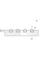
- FIG. 1 is a cross-sectional view schematically showing a solder bump forming member according to an embodiment.
- FIG. 2A is a view of the solder particles viewed from the side opposite to the opening of the recess in FIG. 1, and
- FIG. 2B is a quadrangle circumscribing the projected image of the solder particles created by two pairs of parallel lines. It is a figure which shows the distance X and Y (where Y ⁇ X) between the opposite sides in the case of.
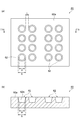
- FIG. 3A is a plan view schematically showing an example of the substrate, and FIG. 3B is a cross-sectional view taken along the line Ib-Ib of FIG. 3A.
- FIG. 4 (a) to 4 (h) are cross-sectional views schematically showing an example of the cross-sectional shape of the concave portion of the substrate.
- FIG. 5 is a cross-sectional view schematically showing a state in which solder fine particles are contained in the recesses of the substrate.
- 6 (a) and 6 (b) are cross-sectional views schematically showing an example of a manufacturing process of an electrode substrate with solder bumps.
- 7 (a) and 7 (b) are cross-sectional views schematically showing an example of a manufacturing process of the connection structure.
- FIG. 8 (a) is an SEM image of a part of the gold bump of the chip C4, and
- FIG. 8 (b) shows the solder bump forming member of Production Example 8 on the gold bump of the chip C4. It is an SEM image after forming a solder bump.
- FIG. 9 is a cross-sectional view schematically showing an example of the substrate.
- each component in the composition means the total amount of the plurality of substances present in the composition when a plurality of substances corresponding to each component are present in the composition, unless otherwise specified.
- the numerical range indicated by using "-" indicates a range including the numerical values before and after "-" as the minimum value and the maximum value, respectively.
- the upper limit value or the lower limit value of the numerical range of one step may be replaced with the upper limit value or the lower limit value of the numerical range of another step.
- the upper limit value or the lower limit value of the numerical range may be replaced with the value shown in the examples.
- the solder bump forming member includes a substrate having a plurality of recesses and solder particles in the recesses, and the average particle size of the solder particles is 1 to 35 ⁇ m. V. The value is 20% or less, and a part of the solder particles protrudes from the recess. Further, in one embodiment, the solder bump forming member includes a substrate having a plurality of recesses and solder particles in the recesses, and the average particle size of the solder particles is 1 to 35 ⁇ m. V. When the value is 20% or less, the depth of the recess is H 1 and the height of the solder particles is H 2 , in cross-sectional view, H 1 ⁇ H 2 .
- FIG. 1 is a cross-sectional view schematically showing a solder bump forming member according to an embodiment.
- the solder bump forming member 10 includes a base 60 having a plurality of recesses 62, and solder particles 1 in the recesses 62. In a predetermined vertical cross section of the solder bump forming member 10, one solder particle 1 is arranged so as to be arranged in a horizontal direction (horizontal direction in FIG. 1) in a state of being separated from one adjacent solder particle 1. The solder particles 1 may be in contact with the side surface and / or the bottom surface thereof in the recess 62.
- the solder bump forming member may be in the form of a film (solder bump forming film), sheet form (solder bump forming sheet), or the like.
- solder bump forming member 10 a part of the solder particles 1 protrudes from the recess. It can be said that at least the top of the solder particles 1 protrudes from the recess 62 of the solder bump forming member 10 (protrudes from the main surface of the substrate 60). Specifically, in a cross-sectional view perpendicular to the main surface of the solder bump forming member 10, when the depth of the recess 62 is H 1 and the height of the solder particles 1 is H 2 , H 1 ⁇ H 2 . is there. The height H 2 of the solder particles 1 refers to the length from the bottom surface of the recess 62 in the cross-sectional view to the top of the solder particles 1.
- the ratio of H 2 to H 1 a (H 2 / H 1) can be 1.02 or more , 1.07 or more.
- the upper limit of the ratio may be 3.00 from the viewpoint of suppressing the falling off of the solder particles 1.
- solder particles The average particle size of the solder particles 1 is, for example, 35 ⁇ m or less, preferably 30 ⁇ m or less, 25 ⁇ m or less, 20 ⁇ m or less, or 15 ⁇ m or less.
- the average particle size of the solder particles 1 is, for example, 1 ⁇ m or more, preferably 2 ⁇ m or more, more preferably 3 ⁇ m or more, and further preferably 5 ⁇ m or more.
- the average particle size of the solder particles 1 can be measured by using various methods according to the size. For example, a dynamic light scattering method, a laser diffraction method, a centrifugal sedimentation method, an electrical detection band method, a resonance type mass measurement method, or the like can be used. Further, a method of measuring the particle size from an image obtained by an optical microscope, an electron microscope, or the like can be used. Specific devices include a flow-type particle image analyzer, a microtrack, a Coulter counter, and the like.
- the average particle diameter of the solder particles 1 is the diameter equivalent to the projected area circle (a circle having an area equal to the projected area of the particles) when the solder particles 1 are observed from a direction perpendicular to the main surface of the solder bump forming member 10. Diameter).
- C. of solder particles 1 V The value is preferably 20% or less, more preferably 10% or less, still more preferably 7% or less, from the viewpoint of achieving more excellent conductivity reliability and insulation reliability.
- the lower limit of the value is not particularly limited.
- C.I. V. The value may be 1% or more, and may be 2% or more.
- FIG. 2A is a view of the solder particles 1 viewed from the side opposite to the opening of the recess 62 in FIG.
- the solder particles 1 have a shape in which a flat surface portion 11 having a diameter A is formed on a part of the surface of a sphere having a diameter B.
- the solder particles 1 shown in FIGS. 1 and 2A have a flat surface portion 11 because the bottom portion of the recess 62 is flat, but when the bottom portion of the recess 62 has a shape other than a flat surface, the shape of the bottom portion is formed. It will have a surface with a different shape corresponding to.
- a flat surface portion 11 may be formed on a part of the surface of the solder particles 1, and at this time, the surface other than the flat surface portion 11 is preferably spherical crown-shaped. That is, the solder particles 1 may have a flat surface portion 11 and a spherical crown-shaped curved surface portion.
- the ratio (A / B) of the diameter A of the flat surface portion 11 to the diameter B of the solder particles 1 may be, for example, more than 0.01 and less than 1.0 (0.01 ⁇ A / B ⁇ 1.0), and is 0. It may be 1 to 0.9.
- the flat surface portion 11 and the bottom surface of the recess 62 may be in contact with each other. As shown in FIG.
- the solder particles 1 have a flat surface portion 11, and the flat surface portion and the bottom surface of the recess 62 are in contact with each other, so that the solder particles 1 are removed from the solder bump forming member 10. Separation is less likely to occur.
- the flat surface portion may also be generated in the portion where the inner wall portion of the recess 62 and the solder particles 1 are in contact with each other.
- the ratio of Y to X (Y).
- / X) may be more than 0.8 and less than 1.0 (0.8 ⁇ Y / X ⁇ 1.0), and may be 0.9 or more and less than 1.0.
- solder particles 1 can be said to be particles closer to a true sphere. Since the solder particles 1 are close to a true sphere, the contact between the solder particles 1 and the electrodes is less likely to be uneven, and a stable connection tends to be obtained. Further, if the volume of the solder particles 1 has little variation, the bonding to the electrode is likely to be stable.
- FIG. 2B is a diagram showing distances X and Y (where Y ⁇ X) between opposite sides when a quadrangle circumscribing the projected image of the solder particles is created by two pairs of parallel lines.
- a quadrangle circumscribing the projected image of the solder particles is created by two pairs of parallel lines.
- an arbitrary particle is observed with a scanning electron microscope to obtain a projected image.
- Two pairs of parallel lines are drawn with respect to the obtained projected image, and the pair of parallel lines are arranged at the position where the distance between the parallel lines is the minimum, and the other pair of parallel lines are arranged at the position where the distance between the parallel lines is the maximum.
- Find the Y / X of the particle This operation is performed on 300 solder particles, the average value is calculated, and the Y / X of the solder particles is obtained.
- the solder particles 1 may contain tin or a tin alloy.
- tin alloy for example, In—Sn alloy, In—Sn—Ag alloy, Sn—Au alloy, Sn—Bi alloy, Sn—Bi—Ag alloy, Sn—Ag—Cu alloy, Sn—Cu alloy and the like are used. be able to. Specific examples of these tin alloys include the following examples.
- the solder particles may contain indium or an indium alloy.
- the indium alloy for example, an In—Bi alloy, an In—Ag alloy, or the like can be used. Specific examples of these indium alloys include the following examples. -In-Bi (In66.3% by mass, Bi33.7% by mass, melting point 72 ° C.) -In-Bi (In33.0% by mass, Bi67.0% by mass, melting point 109 ° C) -In-Ag (In97.0% by mass, Ag3.0% by mass, melting point 145 ° C)
- the tin alloy or indium alloy can be selected according to the application (temperature at the time of connection) of the solder particles 1.
- an In—Sn alloy or a Sn—Bi alloy may be adopted, and in this case, the solder particles can be fused at 150 ° C. or lower.
- a material having a high melting point such as Sn—Ag—Cu alloy or Sn—Cu alloy is used, high reliability can be maintained even after being left at a high temperature.
- the solder particles 1 may contain one or more selected from Ag, Cu, Ni, Bi, Zn, Pd, Pb, Au, P and B.
- Ag or Cu may be contained from the following viewpoints. That is, when the solder particles 1 contain Ag or Cu, the melting point of the solder particles 1 can be lowered to about 220 ° C., and the bonding strength with the electrodes is further improved, so that better conduction reliability can be obtained. It becomes easy to obtain.
- the Cu content of the solder particles 1 is, for example, 0.05 to 10% by mass, and may be 0.1 to 5% by mass or 0.2 to 3% by mass.
- the Cu content is 0.05% by mass or more, it becomes easy to achieve better solder connection reliability.
- the solder particles 1 have a low melting point and excellent wettability, and as a result, the connection reliability of the joint portion by the solder particles 1 tends to be good.
- the Ag content of the solder particles 1 is, for example, 0.05 to 10% by mass, and may be 0.1 to 5% by mass or 0.2 to 3% by mass.
- the Ag content is 0.05% by mass or more, it becomes easy to achieve better solder connection reliability.
- the Ag content is 10% by mass or less, the solder particles 1 have a low melting point and excellent wettability, and as a result, the connection reliability of the joint portion by the solder particles 1 tends to be good.
- the material constituting the substrate 60 for example, an inorganic material such as silicon, various ceramics, glass, a metal such as stainless steel, and an organic material such as various resins can be used.
- the substrate 60 may be a material having heat resistance that does not deteriorate at the melting temperature of the solder fine particles.
- the substrate 60 may be made of a material having heat resistance that does not deform even at the temperature at which the solder fine particles are melted.
- the substrate 60 may be a material that does not change by alloying with a material constituting the solder fine particles or by reacting with the material.
- the recess 62 of the substrate 60 can be formed by a known method such as a cutting method, a photolithography method, or an imprint method.
- a cutting method such as a cutting method, a photolithography method, or an imprint method.
- the recess 62 having an accurate size can be formed in a short process.
- the surface of the substrate 60 may have a coating layer.
- the coating layer may be a material that is difficult or not alloyed with the material constituting the solder fine particles.
- an inorganic substance or an organic substance can be used as the coating layer.
- the coating layer includes inorganic substances having a strong oxide layer on the surface such as aluminum and chromium, oxides such as titanium oxide, nitrides such as boron nitride, carbon-based materials such as diamond-like carbon, diamond and graphite, and fluororesins. Highly heat-resistant resin such as polyimide can be used.
- the coating layer may have a role of adjusting the wettability with the solder. By providing the coating layer on the surface of the substrate 60, the wettability with the solder can be appropriately adjusted according to the purpose of use.
- the coating layer As a method for forming the coating layer, laminating, solution dipping, coating, painting, impregnation, sputtering, plating, etc. can be used.
- the material of the substrate 60 may be an electrode for transferring the solder particles and a material having similar or the same physical characteristics as the substrate on which the electrode is formed. For example, if the materials have a similar coefficient of thermal expansion (CTE) or the same material, misalignment is unlikely to occur during transfer of solder particles.
- CTE coefficient of thermal expansion
- the substrate 60 may be provided with an alignment mark. This alignment mark should be readable by the camera. There may also be an alignment mark on the substrate side having the electrodes. By providing the alignment mark of the base 60 and the substrate having the electrode, when the solder particles are transferred onto the electrode, the alignment mark on the base 60 and the substrate having the electrode are provided by the camera mounted on the alignable device. By reading the alignment mark, it is possible to accurately grasp the position of the recess 62 having the solder particles and the position of the electrode that transfers the solder particles. Further, by providing the alignment mark of the substrate 60 and the substrate having the electrode, the solder particles can be transferred onto the electrode with high positional accuracy.
- the substrate 60 may be made of an organic material.
- the organic material may be a polymer material, and thermoplastic, thermosetting, photocurable materials and the like can be used.
- an organic material By using an organic material, the range of choice of physical properties is widened, so that it is easy to form the substrate 60 according to the purpose.
- the substrate 60 (including the recess 62) can be easily bent or stretched.
- various methods can be used for forming the recess 62. As a method for forming the recess 62, imprint, photolithography, cutting, laser machining, or the like can be used.
- a mold having a desired shape can be pressed against a substrate 60 made of an organic material to form an arbitrary shape on the surface.
- a concave portion 62 having a desired pattern can be formed.
- a photocurable resin can be used to form the recess 62, and when the photocurable resin is applied to the mold (mold), exposed, and then the mold (mold) is peeled off, a substrate 60 having the recess 62 is formed. it can.
- the recess 62 can be formed by a drill or the like.
- the substrate may be composed of a plurality of organic materials. Further, the substrate may have a plurality of layers, and the plurality of layers may be made of different organic materials.
- the organic material may be a polymer material, and thermoplastic, thermosetting, photocurable materials and the like can be used.
- the substrate has two layers made of an organic material, and a recess may be formed in the organic material layer on one side. By forming multiple layers, it is possible to select each material by dividing the function, such as selecting a material having an appropriate wettability with the solder for the material of the recess that comes into contact with the solder.
- FIG. 9 is a cross-sectional view schematically showing an example of a substrate.
- the substrate 600 includes a base layer 601 and a recessed layer 602.
- the base layer 601 is a layer that supports the recess layer 602, and the recess layer 602 is a layer on which the recess 62 is formed by processing.
- a resin material having excellent heat resistance and dimensional stability can be used for the base layer 601, and a material having excellent workability of the recess 62 can be selected for the recess layer 602.
- a thermoplastic resin such as polyethylene terephthalate or polyimide can be used for the base layer 601 and a thermosetting resin capable of forming the recess 62 by an imprint mold can be used for the recess layer 602.
- a substrate 600 (including the recess 62) having excellent flatness can be obtained by sandwiching a thermosetting resin between polyethylene terephthalate and an imprint mold and heating and pressurizing the resin.
- a material having high light transmittance may be used for the base layer 601.
- the material having high light transparency may be, for example, polyethylene terephthalate, transparent (colorless type) polyimide, polyamide or the like.
- the recess 62 is formed using a photocurable material
- a photocurable material for example, an appropriate amount of the photocurable material is applied to the surface of the imprint mold, a polyethylene terephthalate film is placed on the surface, and the recess 62 is added by a roller from the polyethylene terephthalate side. Irradiate ultraviolet light while pressing. Then, after the photocurable material is cured, the imprint mold is peeled off to obtain a substrate 600 having a layer of polyethylene terephthalate and a layer of the photocurable material, and the recess 62 formed of the photocurable material. be able to.
- the material composition of the inner wall and the bottom of the recess 62 can be changed.
- the inner wall and the bottom of the recess 62 may be made of the same resin material. Further, the inner wall and the bottom of the recess 62 may be made of different resin materials (for example, a thermosetting material and a thermoplastic material).
- a photosensitive material may be used as the organic material.
- the photosensitive material may be a positive type photosensitive material or a negative type photosensitive material.
- the recess 62 can be easily formed by forming a photosensitive material having a uniform thickness on the surface of a thermoplastic polyethylene terephthalate film and performing exposure and development.
- the method using exposure and development is widely used in the manufacture of semiconductors, wiring boards, etc., and is a highly versatile method.
- a direct drawing method such as a direct laser exposure.
- the material of the base layer 601 thicker than the thickness of the material forming the concave layer 602
- the physical characteristics of the entire substrate 600 can be dominated by the characteristics of the material of the base layer 601.
- the material of the base layer 601 can compensate for the weakness.
- a material that is hard to heat-shrink is selected as the material of the base layer 601 and the thickness of the base layer 601 is set to be larger than the thickness of the material forming the concave layer 602.
- a combination of a resin material having excellent heat resistance or dimensional stability and a material in which components are less likely to elute at the melting temperature of solder fine particles, and a resin material having excellent heat resistance or dimensional stability and wettability with solder can be obtained.
- An organic material can be appropriately selected according to the purpose, such as a combination with an appropriate material.
- the substrate may be a substrate 600 composed of a base layer 601 and a recessed layer 602.
- the recess layer 602 as a photosensitive material, the recess 62 can be produced by photolithography.
- the recess layer 602 By using a light or thermosetting material, a thermoplastic material, or the like for the recess layer 602, the recess 62 can be easily produced by the imprint method. Further, since the characteristics of the entire substrate can be adjusted by changing the thickness of the base layer 601, there is an advantage that a substrate having desired characteristics can be produced.
- the substrate 60 may be made of an inorganic material.
- silicon silicon wafer
- stainless steel aluminum and the like can be used as the inorganic material.
- contamination countermeasures are easy, and they can contribute to high yield and stable production.
- solder particles formed in the recess 62 are transferred to an electrode on a silicon wafer, if the substrate 60 is made of a silicon wafer, a material having a similar CTE or the same material will be used. As a result, misalignment, warpage, etc.
- a method for forming the recess 62 processing by laser, cutting or the like, dry etching or wet etching method, electron beam drawing (for example, FIB processing) or the like can be used. Dry etching is widely used in the production of semiconductors, MEMS, etc., and can process inorganic materials with high accuracy on the order of microns to nano.
- the substrate 60 glass, quartz, sapphire or the like can be used. Since these materials are transparent, they can be easily aligned when the solder particles in the recess 62 are transferred to another substrate on which the electrodes are formed.
- processing by laser, cutting or the like dry etching or wet etching method, electron beam drawing (for example, FIB processing) or the like can be used.
- the advantage of using an inorganic material is that it is superior in dimensional stability compared to an organic material.
- the solder particles in the recess 62 are transferred onto the electrode, they can be transferred with high positional accuracy. For example, when transferring solder particles to a plurality of electrodes having a size and pitch on the order of micrometers, if an inorganic material having excellent dimensional stability is used, the solder particles can be transferred to the same position on any of the electrodes.
- the substrate may be composed of a plurality of materials. Further, the substrate may have a plurality of layers, and the plurality of layers may be made of different materials.
- the organic-inorganic composite material for example, a combination of an inorganic material and an inorganic material, or a combination of an inorganic material and an organic material can be used. The combination of the inorganic material and the organic material can achieve both dimensional stability and workability of the recess 62.
- Examples of the substrate having a combination of an inorganic material and an organic material include a substrate having a base layer 601 made of a metal such as silicon, various ceramics, glass, and stainless steel, which is an inorganic material, and a concave layer 602 made of an organic material. Can be mentioned.
- a substrate can be obtained, for example, by forming a photosensitive material on the surface of a silicon wafer and forming recesses by exposure and development.
- the inner wall and bottom of the recess 62 may be made of a photosensitive material, or the inner wall of the recess 62 may be made of a photosensitive material and the bottom may be made of a silicon wafer.
- the configuration of the recess 62 can be appropriately selected according to the purpose such as wettability with the solder particles in the recess 62 and ease of transfer to the electrode.
- a photosensitive material layer is further provided on the surface of the silicon wafer by forming a photosensitive material on the surface of the silicon wafer and curing it, and the surface of the layer is provided with a layer of the photosensitive material.
- a method of providing the recess 62 by forming a photosensitive material again and performing exposure and development can be used.
- the photosensitive material on the surface side of the silicon wafer and the photosensitive material provided on the outermost layer may have different compositions.
- the photosensitive material can be appropriately selected in consideration of the wettability and stainability of the solder particles.
- the surface of the photosensitive material layer on the outermost layer may come into contact with the electrode or the surface of the substrate having the electrode. Therefore, a photosensitive material that does not damage the electrode and the substrate or does not contaminate the electrode and the substrate can be appropriately selected.
- the photosensitive material may be a material that prevents elution of uncured components and contamination by halogen-based materials, silicone-based materials, and the like. Further, the photosensitive material may be a material having high resistance to a reducing atmosphere, flux, etc. when transferring solder particles to an electrode.
- the photosensitive material may be a material that is resistant to a reducing atmosphere such as formic acid, hydrogen, and hydrogen radicals.
- the photosensitive material may be a material having high resistance to the temperature at which the solder particles are transferred to the electrode.
- the photosensitive material may be a material that is resistant to temperatures of 100 ° C. or higher and 300 ° C. or lower. Since the melting point of the solder particles differs depending on the constituent material, the heat resistant temperature of the photosensitive material can also be selected according to the solder material to be used.
- tin-silver-copper solder eg SAC305 (melting point 219 ° C)
- SAC305 melting point 219 ° C
- a material having heat resistance can be used.
- tin-bismuth solder eg SnBi58 (melting point 139 ° C.)
- a material having a heat resistance of 140 ° C. or higher can be used, and a material having a heat resistance of 160 ° C. or higher can be used industrially. Wider usage likelihood.
- indium solder melting point 159 ° C.
- a material having a heat resistance of 170 ° C. or higher can be used.
- indium-tin solder eg, melting point 120 ° C.
- a material having a heat resistance of 130 ° C. or higher can be used.
- Examples of the other substrate include a substrate having a recess 62 formed of a thermosetting or thermoplastic resin on a stainless steel plate.
- the substrate can be obtained by sandwiching a thermosetting material (resin) between a stainless steel plate and an imprint mold, heating under pressure, and then peeling off the imprint mold.
- Examples of the other substrate include a substrate having a recess 62 formed of a photocurable material on a glass plate.
- the substrate can be obtained by applying a photocurable material on a glass plate and exposing the substrate while pressing the imprint mold to cure the photocurable material and peeling off the imprint mold.
- the material composition of the inner wall and the bottom of the recess 62 can be changed depending on the pressurizing condition.
- the inner wall and the bottom of the recess 62 can be made of the same resin material.
- the inner wall of the recess 62 can be made of a resin material and the bottom can be made of an inorganic material.
- a composite material containing glass fiber, a filler, etc. and a resin component can also be used.
- the composite material include a copper-clad laminate for a wiring board and the like.
- a photosensitive material, a thermosetting resin, a photocurable resin, or the like can be applied to the surface of the copper-clad laminate to form the recess 62 as described above.
- the copper-clad laminate mainly contains a large amount of resin material, the CTE can be lowered by combining with glass fiber, various fillers, and the like, so that the above-mentioned dimensional stability can be ensured.
- the recess 62 is also formed on the same copper-clad laminate so that the CTEs of both become the same or close to each other, and the position at the time of transferring the solder particles in the recess 62 is obtained. It has the advantage of being easy to align and less likely to cause misalignment.
- a packaging encapsulant can also be used as the material for the recess layer 602.
- the sealing material any solid, liquid or film form can be used.
- the recess 62 can be formed by laminating a sealing material on a glass, silicon wafer, or the like in a thin layer and pressurizing and heating with an imprint mold.
- the method for manufacturing the solder bump forming member 10 includes a preparatory step of preparing a substrate having a plurality of recesses and solder fine particles, a storage step of accommodating at least a part of the solder fine particles in the recesses, and a method of accommodating the solder fine particles contained in the recesses. It is a fusion step of fusing to form solder particles in the recess, and includes a step in which a part of the solder particles protrudes from the recess.
- FIG. 3A is a plan view schematically showing an example of the substrate 60
- FIG. 3B is a cross-sectional view taken along the line Ib-Ib of FIG. 3A.
- the substrate 60 shown in FIG. 3A has a plurality of recesses 62.
- the plurality of recesses 62 may be regularly arranged in a predetermined pattern.
- the positions and numbers of the plurality of recesses 62 may be set according to the shape, size, pattern, etc. of the electrodes to be connected.
- the distance L between adjacent recesses is not particularly limited, but can be 0.1 times or more the average particle size of the contained solder particles, and may be 0.2 times or more.
- the upper limit of the value can be, for example, 0.3 times.
- the distance between the recesses is not the distance between the centers of the recesses, but the distance from the edge of the recess opening to the edge.
- the recess 62 of the base 60 is preferably formed in a tapered shape in which the opening area expands from the bottom 62a side of the recess 62 toward the surface 60a side of the base 60. That is, as shown in FIGS. 3A and 3B, the width of the bottom 62a of the recess 62 (the width a in FIGS. 3A and 3B) is the opening at the surface 60a of the recess 62. Is preferably narrower than the width of (width b in FIGS. 3 (a) and 3 (b)).
- the size of the recess 62 may be set according to the size of the target solder particles.
- the shape of the recess 62 may be a shape other than the shapes shown in FIGS. 3 (a) and 3 (b).
- the shape of the opening on the surface 60a of the recess 62 may be an ellipse, a triangle, a quadrangle, a polygon, or the like, in addition to the circular shape as shown in FIG. 3A.
- the shape of the recess 62 in the cross section perpendicular to the surface 60a may be, for example, the shape shown in FIG. 4 (a) to 4 (h) are cross-sectional views schematically showing an example of the cross-sectional shape of the concave portion of the substrate.
- the width (width b) of the opening on the surface 60a of the recess 62 is the maximum width in the cross-sectional shape.
- the width (width b) of the opening is the maximum width in the cross-sectional shape, when the solder particles 1 are transferred onto the electrodes, the solder particles 1 can easily come out from the recess 62, and the transfer rate is improved. Can be expected. Further, by appropriately adjusting the width (width b) of the opening, the position shift when the solder particles 1 are transferred onto the electrodes is less likely to occur, and the solder bumps are easily formed at the correct positions.
- the solder fine particles prepared in the preparatory step may contain fine particles having a particle size smaller than the width (width b) of the opening on the surface 60a of the recess 62, and may contain more fine particles having a particle size smaller than the width b. Is preferable.
- the D10 particle size of the particle size distribution is preferably smaller than the width b
- the D30 particle size of the particle size distribution is more preferably smaller than the width b
- the D50 particle size of the particle size distribution is smaller than the width b. More preferred.
- the particle size distribution of the solder fine particles can be measured using various methods according to the size. For example, a dynamic light scattering method, a laser diffraction method, a centrifugal sedimentation method, an electrical detection band method, a resonance type mass measurement method, or the like can be used. Further, a method of measuring the particle size from an image obtained by an optical microscope, an electron microscope, or the like can be used. Specific devices include a flow-type particle image analyzer, a microtrack, a Coulter counter, and the like.
- the value is not particularly limited, but from the viewpoint of improving the filling property into the recess 62 by the combination of large and small fine particles, C.I. V.
- the value is preferably high.
- C.I. V. The value may exceed 20%, preferably 25% or more, more preferably 30% or more.
- V. The value is calculated by dividing the standard deviation of the particle size measured by the above method by the average particle size (D50 particle size) and multiplying by 100.
- the solder fine particles may contain tin or a tin alloy.
- tin alloy for example, In—Sn alloy, In—Sn—Ag alloy, Sn—Au alloy, Sn—Bi alloy, Sn—Bi—Ag alloy, Sn—Ag—Cu alloy, Sn—Cu alloy and the like are used. be able to. Specific examples of these tin alloys include the following examples.
- the solder fine particles may contain indium or an indium alloy.
- the indium alloy for example, an In—Bi alloy, an In—Ag alloy, or the like can be used. Specific examples of these indium alloys include the following examples. -In-Bi (In66.3% by mass, Bi33.7% by mass, melting point 72 ° C.) -In-Bi (In33.0% by mass, Bi67.0% by mass, melting point 109 ° C) -In-Ag (In97.0% by mass, Ag3.0% by mass, melting point 145 ° C)
- the above tin alloy or indium alloy can be selected according to the application (temperature at the time of use) of the solder particles.
- an In—Sn alloy or a Sn—Bi alloy may be adopted.
- solder particles that can be fused at 150 ° C. or lower can be obtained.
- a material having a high melting point such as Sn—Ag—Cu alloy or Sn—Cu alloy is used, solder particles capable of maintaining high reliability even after being left at a high temperature can be obtained.
- the solder fine particles may contain one or more selected from Ag, Cu, Ni, Bi, Zn, Pd, Pb, Au, P and B.
- Ag or Cu may be contained from the following viewpoints. That is, when the solder fine particles contain Ag or Cu, the melting point of the obtained solder particles can be lowered to about 220 ° C., and the solder particles having excellent bonding strength with the electrode can be obtained, so that better conduction reliability can be obtained. The effect of obtaining sex is achieved.
- the Cu content of the solder fine particles is, for example, 0.05 to 10% by mass, and may be 0.1 to 5% by mass or 0.2 to 3% by mass.
- the Cu content is 0.05% by mass or more, it becomes easy to obtain solder particles capable of achieving good solder connection reliability. Further, when the Cu content is 10% by mass or less, solder particles having a low melting point and excellent wettability can be easily obtained, and as a result, the connection reliability of the electrode with solder bumps tends to be improved.
- the Ag content of the solder fine particles is, for example, 0.05 to 10% by mass, and may be 0.1 to 5% by mass or 0.2 to 3% by mass.
- the Ag content is 0.05% by mass or more, it becomes easy to obtain solder particles capable of achieving good solder connection reliability.
- the Ag oil content is 10% by mass or less, solder particles having a low melting point and excellent wettability can be easily obtained, and as a result, the connection reliability of the electrode with solder bumps tends to be improved.
- the solder fine particles prepared in the preparatory step are accommodated in each of the recesses 62 of the substrate 60.
- the accommodating step may be a step of accommodating all the solder fine particles prepared in the preparatory step into the recess 62, and a part of the solder fine particles prepared in the preparatory step (for example, the width b of the opening of the recess 62 among the solder fine particles). It may be a step of accommodating a smaller particle) in the recess 62.
- FIG. 5 is a cross-sectional view schematically showing a state in which the solder fine particles 111 are housed in the recess 62 of the substrate 60. As shown in FIG. 5, a plurality of solder fine particles 111 are housed in each of the plurality of recesses 62.
- the degree of protrusion of the solder particles 1 can be adjusted.
- the amount of the solder fine particles 111 contained in the recess 62 is, for example, preferably 20% or more, more preferably 30% or more, still more preferably 50% or more, based on the volume of the recess 62. , 60% or more is most preferable. As a result, a part of the solder particles can be projected from the recess 62. Further, the variation in the accommodating amount is suppressed, and it becomes easy to obtain solder particles having a smaller particle size distribution.
- solder materials have the property of forming a spherical shape due to their own surface tension when they are in a molten state in an environment above the melting point.
- the solder fine particles 111 housed in the recess 62 are combined into the solder particles 1 by a fusion process described later.
- the height of the obtained solder particles 1 becomes higher than the depth of the recess 62, and the solder particles 1 protrude from the recess 62. Therefore, if the diameter of the solder particles 1 is larger than the depth of the recess 62, the solder particles 1 protrude from the recess 62. Since the diameter of the solder particles 1 can be adjusted by the shape of the recess 62 and the amount of the solder fine particles 111 accommodated in the recess 62, the degree of protrusion from the recess 62 can be adjusted accordingly.
- solder fine particles 111 are melted in the fusion step described later, wet spread occurs in the bottom portion and the inner wall portion depending on the material of the bottom portion and the inner wall portion of the recess 62, and at least a part of the solder particles 1 is covered with the recess 62. A part in contact with the bottom and / or the inner wall is generated. As a result, a flat surface portion may be generated on at least a part of the solder particles 1.
- the size of the flat surface portion differs depending on the combination of the surface materials of the bottom portion and the inner wall portion of the recess 62 and the solder composition constituting the solder fine particles 111.
- the form of the solder particles 1 is a true sphere, an ellipsoid, a flat sphere, a form having a flat portion in a part, or the like.
- an inorganic substance such as glass or silicon, or an organic substance such as plastic or resin can be used, and the bottom and inner wall portions of such a material generally tend to have low wettability with solder, and the solder particles 1 have a tendency to have low wettability with solder. It tends to have a spherical shape that is close to a true sphere. Therefore, assuming that the solder particles 1 are spheres close to a true sphere, the height of the solder particles 1 can be approximated to the diameter of the solder particles 1. Since the diameter of the solder particles 1 can be calculated from the total volume of the solder particles 111 filled in the recesses 62, the amount of the solder particles 111 required for the solder particles 1 to protrude from the recesses 62 can be calculated.
- solder fine particles 111 filled in the recess 62 are melted and united to form the solder particles 1, and the solder particles 1 are spherical, the solder fine particles 111 required for the solder particles 1 to protrude from the recess 62.
- the quantity can be indicated.
- the aspect ratio of the recess is represented by L / D.
- the filling ratio of the solder fine particles 111 into the recess 62 is 66% by volume or more when the aspect ratio is 1, 38% by volume or more when the aspect ratio is 0.75, and 17 volumes when the aspect ratio is 0.5. % Or more, preferably 5% by volume or more when the aspect ratio is 0.25.
- the average particle size, particle size, etc. of the solder fine particles 111 is selected according to the size of the recess 62 and the ratio of the diameter to the depth (aspect ratio). For example, when the diameter of the recess 62 is 4 ⁇ m and the depth is 4 ⁇ m (aspect ratio is 1), the filling amount of the recess 62 varies by using the solder fine particles 111 having an average particle diameter of 1 to 2 ⁇ m or less. The variation in the diameter of the obtained solder particles 1 can be suppressed, and the variation in the amount of protrusion (height) from the recess 62 can be easily suppressed.
- the bottom shape of the recess 62 in order to make it easier to unite. For example, it is preferable to select a bottom shape having a slope toward the center as shown in FIGS. 4 (b), (e), (g), and (h).
- the aspect ratio of the recess 62 is large, in other words, when the recess 62 has a wide opening width and a shallow shape, when the solder fine particles 111 are melted, the solder fine particles 111 that remain without being united are generated.
- the method of accommodating the solder fine particles in the recess 62 is not particularly limited.
- the accommodating method may be either dry or wet.
- the solder fine particles prepared in the preparation step are placed on the substrate 60, and the surface 60a of the substrate 60 is rubbed with a squeegee to remove the excess solder fine particles while accommodating sufficient solder fine particles in the recess 62. can do.
- the width b of the opening of the recess 62 is larger than the depth of the recess 62, solder fine particles may pop out from the opening of the recess 62.
- a squeegee is used, the solder fine particles protruding from the opening of the recess 62 are removed.
- Examples of the method of removing the excess solder fine particles include a method of blowing compressed air, a method of rubbing the surface 60a of the substrate 60 with a non-woven fabric or a bundle of fibers, and the like. Since these methods have a weaker physical force than the squeegee, they are preferable for handling easily deformable solder fine particles. Further, in these methods, the solder fine particles protruding from the opening of the recess 62 can be left in the recess.
- the fusion step is a step of fusing the solder fine particles 111 contained in the recess 62 (for example, by heating to 130 to 260 ° C.) to form the solder particles 1 in the recess 62, which is partially protruding from the recess 62.
- the solder fine particles 111 housed in the recess 62 are united by melting and spheroidized by surface tension.
- the molten solder follows the bottom portion 62a to form the flat surface portion 11.
- the formed solder particles 1 have a shape having a flat surface portion 11 on a part of the surface. In this way, the solder bump forming member 10 shown in FIG. 1 is obtained.
- Examples of the method of melting the solder fine particles 111 contained in the recess 62 include a method of heating the solder fine particles 111 to a temperature equal to or higher than the melting point of the solder. Due to the influence of the oxide film, the solder fine particles 111 may not melt or spread even when heated at a temperature equal to or higher than the melting point, and may not be united. Therefore, the solder fine particles 111 are exposed to a reducing atmosphere to remove the surface oxide film of the solder fine particles 111, and then heated to a temperature equal to or higher than the melting point of the solder fine particles 111 to melt the solder fine particles 111 and spread them wet. It can be unified.
- the solder fine particles 111 are melted in a reducing atmosphere.
- the method for manufacturing the solder bump forming member may further include a reduction step of exposing the solder fine particles contained in the recesses to the reducing atmosphere before the fusion step. Further, in the fusion step of the method for manufacturing the solder bump forming member, the solder fine particles may be fused in a reducing atmosphere.
- the method for creating a reducing atmosphere is not particularly limited as long as the above effects can be obtained, and for example, there is a method using hydrogen gas, hydrogen radical, formic acid gas, or the like.
- a hydrogen reduction furnace, a hydrogen radical reduction furnace, a formic acid reduction furnace, or a conveyor furnace or a continuous furnace thereof the solder fine particles 111 can be melted in a reducing atmosphere.
- These devices may be equipped with a heating device, a chamber filled with an inert gas (nitrogen, argon, etc.), a mechanism for evacuating the inside of the chamber, etc., which makes it easier to control the reducing gas. Become. Further, if the inside of the chamber can be evacuated, the voids can be removed by reducing the pressure after the solder fine particles 111 are melted and united, and the solder particles 1 having further excellent connection stability can be obtained.
- Profiles such as reduction, melting conditions, temperature, and atmosphere adjustment in the furnace of the solder fine particles 111 may be appropriately set in consideration of the melting point, particle size, recess size, material of the substrate 60, and the like of the solder fine particles 111.
- the substrate 60 in which the solder fine particles 111 are filled in the recesses is inserted into the furnace, vacuumed, and then the reducing gas is introduced to fill the inside of the furnace with the reducing gas, and the surface oxide film of the solder fine particles 111 is formed.
- the reducing gas is removed by vacuuming, and then the gas is heated to a temperature equal to or higher than the melting point of the solder fine particles 111 to dissolve and coalesce the solder fine particles to form the solder particles in the recess 62. After filling with nitrogen gas, the temperature inside the furnace is returned to room temperature to obtain solder particles 1. Further, for example, the substrate 60 in which the solder fine particles 111 are filled in the recesses is inserted into the furnace, and after vacuuming, the reducing gas is introduced to fill the inside of the furnace with the reducing gas, and the in-core heater is used.
- the solder fine particles 111 are heated to remove the surface oxide film of the solder fine particles 111, then the reducing gas is removed by vacuuming, and then the solder fine particles 111 are heated to the melting point or higher to dissolve and coalesce the solder fine particles. After forming the solder particles in the recess 62, the temperature inside the furnace is returned to room temperature after filling with nitrogen gas to obtain the solder particles 1.
- the substrate 60 in which the solder fine particles 111 are filled in the recesses is inserted into the furnace, and after vacuuming, the reducing gas is introduced to fill the inside of the furnace with the reducing gas, and the in-core heater is used.
- the reducing gas is introduced to fill the inside of the furnace with the reducing gas, and the in-core heater is used.
- the surface oxide film of the solder fine particles 111 is removed by reduction, and at the same time, the solder fine particles are melted and united to form solder particles in the recess 62, which is reduced by vacuuming.
- the temperature in the furnace is returned to room temperature after filling with nitrogen gas, and the solder particles 1 can be obtained. In this case, since the temperature rise and fall in the furnace need only be adjusted once, there is an advantage that the processing can be performed in a short time.
- the inside of the furnace may be made into a reducing atmosphere again to add a step of removing the surface oxide film that could not be completely removed. As a result, it is possible to reduce residues such as solder fine particles remaining unfused and a part of the oxide film remaining unfused.
- the substrate 60 in which the solder fine particles 111 are filled in the recesses is placed on the conveyor and passed through a plurality of zones in succession to obtain the solder particles 1.
- the substrate 60 in which the solder fine particles 111 are filled in the recesses is placed on a conveyor set at a constant speed and passed through a zone filled with an inert gas such as nitrogen or argon at a temperature lower than the melting point of the solder fine particles 111.
- the surface oxide film of the solder fine particles 111 is removed by passing through a zone in which a reducing gas such as formic acid gas having a temperature lower than the melting point of the solder fine particles 111 exists, and then nitrogen or nitrogen having a temperature equal to or higher than the melting point of the solder fine particles 111 is removed.
- the solder fine particles 111 are melted and coalesced by passing through a zone filled with an inert gas such as argon, and then passed through a cooling zone filled with an inert gas such as nitrogen or argon to obtain solder particles 1. be able to.
- the substrate 60 in which the solder fine particles 111 are filled in the recesses is placed on a conveyor set at a constant speed and passed through a zone filled with an inert gas such as nitrogen or argon having a temperature equal to or higher than the melting point of the solder fine particles 111. Subsequently, the surface oxide film of the solder fine particles 111 is removed, melted and coalesced by passing through a zone in which a reducing gas such as formic acid gas having a temperature equal to or higher than the melting point of the solder fine particles 111 exists, and then nitrogen or argon or the like is used.
- the solder particles 1 can be obtained by passing through a cooling zone filled with the inert gas.
- a film-like material can be continuously processed by roll-to-roll.
- a continuous roll product of the substrate 60 in which the solder fine particles 111 are filled in the recesses is produced, a roll unwinder is installed on the inlet side of the conveyor furnace, and a roll winder is installed on the outlet side of the conveyor furnace to maintain a constant speed.
- the solder fine particles 111 filled in the recesses can be fused.
- the solder particles 1 having a uniform size can be formed regardless of the material and shape of the solder fine particles 111.
- indium-based solder can be precipitated by plating, but it is difficult to precipitate it in the form of particles, and it is soft and difficult to handle.
- indium-based solder particles having a uniform particle size can be easily produced.
- the formed solder particles 1 can be handled in a state of being housed in the recess 62 of the substrate 60, the solder particles 1 can be transported and stored without being deformed.
- solder particles 1 are housed in the recesses 62 of the substrate 60, the solder particles can be brought into contact with the electrodes without being deformed.
- the average particle size of the obtained solder particles may be 1 to 35 ⁇ m, and C.I. V. The value may be 20% or less.
- solder fine particles 111 may have a large variation in particle size distribution or a distorted shape, and can be suitably used as a raw material if they can be accommodated in the recess 62.
- the shape of the recess 62 of the substrate 60 can be freely designed by lithography, machining, imprinting technology, or the like. Since the size of the solder particles 1 depends on the amount of the solder fine particles 111 accommodated in the recess 62, the size of the solder particles 1 can be freely designed by designing the recess 62.
- the method for manufacturing an electrode substrate with solder bumps includes a preparatory step for preparing the solder bump forming member and a substrate having a plurality of electrodes, and a surface having a recess of the solder bump forming member and a surface having electrodes of the substrate. It includes an arrangement step of bringing the solder particles and electrodes into contact with each other, and a heating step of heating the solder particles to a temperature equal to or higher than the melting point of the solder particles.
- substrates (circuit members) having a plurality of electrodes on the surface include chip components such as IC chips (semiconductor chips), resistor chips, capacitor chips, and driver ICs; rigid type package substrates. These circuit members are provided with circuit electrodes, and are generally provided with a large number of circuit electrodes.
- substrates having a plurality of electrodes on the surface include wiring substrates such as flexible tape substrates having metal wiring, flexible printed wiring boards, and glass substrates on which indium tin oxide (ITO) is vapor-deposited.
- ITO indium tin oxide
- Electrodes include copper, copper / nickel, copper / nickel / gold, copper / nickel / palladium, copper / nickel / palladium / gold, copper / nickel / gold, copper / palladium, copper / palladium / gold, and copper.
- / Tin, copper / silver, indium tin oxide and other electrodes can be mentioned.
- Electrodes can be formed by electroless plating or electroplating or sputtering or etching of metal foil.
- FIG. 6A and 6 (b) are cross-sectional views schematically showing an example of a manufacturing process of an electrode substrate with solder bumps.
- the substrate 60 shown in FIG. 6A is in a state in which one solder particle 1 is housed in each of the recesses 62.
- the substrate 2 has a plurality of electrodes 3 on the surface.
- the surface of the substrate 60 on the electrode 3 side is opposed to the opening side surface of the recess 62 of the substrate 60, and the substrate 60 is in contact with the solder particles 1 housed in the recess 62 of the substrate 60 until the electrode 3 comes into contact with each other.
- the substrate 2 are brought close to each other (arrows A and B in FIG. 6A).
- the number of solder particles 1 that come into contact with the individual electrodes 3 is not particularly limited, and may be one particle per electrode and may be a plurality of particles per electrode. Since the force acting between the solder particles 1 and the recess 62 (for example, an intermolecular force such as van der Waals force) is larger than the gravity applied to the solder particles 1, it is assumed that the main surface of the substrate 60 is directed downward. However, the solder particles 1 do not fall off and remain in the recess 62. Further, when at least a part of the solder particles 1 is in contact with the bottom portion and / or the inner wall portion of the recess 62 and has a flat surface portion, the solder particles 1 are in close contact with the recess 62 and are difficult to fall off.
- an intermolecular force such as van der Waals force
- the solder particles 1 are melted and solder bumps are formed on the electrode 3.
- the solder particles 1 and the electrode 3 are brought into contact with each other in a pressurized state, and the solder particles 1 are heated to a temperature equal to or higher than the melting point of the solder particles. It's okay.
- the pressurized state is a state in which the solder bump forming member 10 and the substrate 2 are pressed against each other with a force of about 20 to 600 MPa in the directions of arrows A and B in FIG. 6A.
- solder particles 1 may not melt or spread even when heated at a temperature higher than the melting point due to the influence of the oxide film. Therefore, the solder particles 1 can be melted by exposing the solder particles 1 to a reducing atmosphere, removing the surface oxide film of the solder particles 1, and then heating the solder particles 1 to a temperature equal to or higher than the melting point of the solder particles 1. Further, it is preferable that the solder particles 1 are melted in a reducing atmosphere. By heating the solder particles 1 to a temperature equal to or higher than the melting point of the solder particles 1 and creating a reducing atmosphere, the oxide film on the surface of the solder particles 1 is reduced, and the oxide film on the electrode surface is further reduced to melt the solder particles 1. Wetting and spreading can proceed efficiently.
- the method for manufacturing an electrode substrate with solder bumps further includes a reduction step of exposing the solder particles (and / or electrodes) to a reducing atmosphere before the placement step or after the placement step and before the heating step. It's okay.
- the solder particles may be heated to a temperature equal to or higher than the melting point of the solder particles in a reducing atmosphere.
- the electrodes and the opening surfaces of the solder bump forming members are brought into close contact with each other (under pressure if necessary), so that the solder bumps are formed only on the electrodes and the adjacent electrodes. Bridges due to solder between them are easily suppressed.
- the description of the manufacturing method of the solder bump forming member can be referred to as appropriate.
- the method for manufacturing an electrode substrate with solder bumps may further include a removal step of removing the solder bump forming member from the substrate after the heating step.
- the solder bump forming member 10 is removed from the substrate 2 (removal step) to obtain the electrode substrate 20 with solder bumps.
- FIG. 6B is a schematic view of the electrode substrate 20 with solder bumps thus obtained. It is preferable that the solder bump forming member and the surface of the substrate have an alignment mark for easy alignment.
- the position of the recess of the solder bump forming member and the position of the electrode on the surface of the substrate are arranged in advance.
- Solder particles are placed in the recesses of the solder bump forming member, the opening surface side of the recesses of the solder bump forming member and the electrode surface side of the base material are opposed to each other, and the electrode on which the solder bumps are to be formed is formed by using the alignment mark.
- the solder bump can be formed on the electrode by the above-mentioned various methods.
- solder bumps can be formed only on a specific electrode. For example, for a plurality of electrodes on the surface of the base material, by preliminarily providing a recess of the solder bump forming member at a position opposite to the position of the specific electrode, the solder bump can be formed only on the specific electrode on the surface of the base material. Can be formed. Further, one solder bump can be formed on one electrode.
- the method for manufacturing the electrode substrate with solder bumps may further include a cleaning step of removing the solder particles 1 not bonded to the electrode after the removing step.
- the cleaning method include blowing compressed air, rubbing the surface of the substrate with a non-woven fabric or a bundle of fibers, and the like.
- an electrode substrate 20 with solder bumps having a substrate 2, an electrode 3, and a solder bump 1A in this order.
- connection structure 7 (a) and 7 (b) are cross-sectional views schematically showing an example of a manufacturing process of the connection structure.
- a method of manufacturing the connection structure will be described with reference to FIGS. 7 (a) and 7 (b).
- the electrode substrate 20 with solder bumps shown in FIG. 6B is prepared in advance.
- another substrate 4 having a plurality of other electrodes 5 is prepared.
- both are arranged so that the solder bump 1A and the other electrode 5 face each other.
- the solder bump 1A and the other electrode 5 are kept in contact with each other, and the electrode 3 and the other electrode 5 are heated at least to a temperature higher than the melting point of the solder bump 1A (for example, 130 ° C.
- solder bump 1A melts between them. After that, by cooling the whole, a solder layer 1B is formed between the electrode 3 and the other electrodes 5, and the electrodes are electrically connected to each other.
- heat in an atmosphere in which oxygen is blocked For example, heating in an atmosphere of an inert gas such as nitrogen is preferable.
- an inert gas such as nitrogen is preferable.
- a vacuum reflow furnace, a nitrogen reflow furnace, or the like can be used.
- solder bump 1A it is preferable to heat the solder bump 1A in a reducing atmosphere in order to melt the solder bump 1A by heating and more preferably join the opposing electrodes 3 and 5 to each other.
- Hydrogen gas, hydrogen radicals, formic acid and the like can be used to create a reducing atmosphere.
- a hydrogen reduction furnace, a hydrogen reflow furnace, a hydrogen radical furnace, a formic acid furnace, these vacuum furnaces, a continuous furnace, and a conveyor furnace can be used.
- the oxide film on the surface of the solder bump 1A and the oxide film on the surface of the electrode 5 can be reduced and removed, so that the solder bump 1A easily wets and spreads on the electrode 5, and the electrode is passed through the solder layer 1B. A more stable bond is achieved between 3 and the electrode 5.
- the electrode substrate 20 with solder bumps shown in FIG. 6B is prepared in advance. Further, another substrate 4 having a plurality of other electrodes 5 on the surface is prepared. Then, both are arranged so that the solder bump 1A and the other electrode 5 face each other. Then, pressure is applied in the thickness direction of the laminated body of these members (directions of arrows A and B shown in FIG. 7A). By heating the whole to a temperature higher than the melting point of the solder bump 1A (for example, 130 to 260 ° C.) when pressurizing, the solder bump 1A melts between the electrode 3 and the other electrodes 5.
- a temperature higher than the melting point of the solder bump 1A for example, 130 to 260 ° C.
- a solder layer 1B is formed between the electrode 3 and the other electrodes 5, and the electrodes are electrically connected to each other.
- an atmosphere of an inert gas such as nitrogen
- a reducing atmosphere examples include the above-mentioned hydrogen gas, hydrogen radicals, formic acid and the like.
- a hydrogen reduction furnace, a hydrogen reflow furnace, a hydrogen radical furnace, a formic acid furnace, these vacuum furnaces, a continuous furnace, a conveyor furnace, and the like can be used.
- a material having a reducing action can be used as a method of creating a reducing atmosphere.
- a flux material or a material containing a flux component can be arranged in the vicinity of the solder bump 1A or the electrode 5 and the electrode 3.
- a paste, a film or the like containing a flux material and a material containing a flux component can be used.
- the electrode substrate 20 with solder bumps shown in FIG. 6B is prepared in advance.
- a flux material or a paste containing a flux component is arranged on the entire surface of the electrode substrate 20 on which the solder bumps 1A are formed, or in the vicinity of the electrode 3 including the solder bumps 1A and the solder bumps 1A.
- solder bump 1A and the other electrode 5 face each other.
- the solder bump 1A and the other electrode 5 are brought into contact with each other through, for example, a flux material or a paste containing a flux component, and brought to a temperature higher than the melting point of the solder bump 1A (for example, 130 ° C. to 260 ° C.). At least by heating, the solder bump 1A melts between the electrode 3 and the other electrodes 5.
- a solder layer 1B is formed between the electrode 3 and the other electrodes 5, and the electrodes are electrically connected to each other. After that, when the flux component is washed and removed, corrosion of the solder layer 1B, the electrode 3 and the electrode 5 can be suppressed by the flux residue.
- the electrode substrate 20 with solder bumps shown in FIG. 6B is prepared in advance. Further, another substrate 4 having a plurality of other electrodes 5 on the surface is prepared, and a flux material or a paste containing a flux component is arranged on the entire surface of the substrate 4 having the electrodes 5 or near the surface of the electrodes 5. Then, both are arranged so that the solder bump 1A and the other electrode 5 face each other. After that, the solder bump 1A and the other electrode 5 are brought into contact with each other via, for example, a flux material and a paste containing a flux component, and brought to a temperature higher than the melting point of the solder bump 1A (for example, 130 ° C. to 260 ° C.). At least by heating, the solder bump 1A melts between the electrode 3 and the other electrodes 5. After that, by cooling the whole, a solder layer 1B is formed between the electrode 3 and the other electrodes 5, and the electrodes are electrically connected to each other.
- the electrode substrate 20 with solder bumps shown in FIG. 6B is prepared in advance.
- a film containing a flux component is arranged on the surface side of the electrode substrate 20 on which the solder bumps 1A are formed.
- another substrate 4 having a plurality of other electrodes 5 on the surface is prepared. Then, both are arranged so that the solder bump 1A and the other electrode 5 face each other. After that, the solder bump 1A and the other electrode 5 are kept in contact with each other via a film containing a flux component, or a pressure is applied between the opposing electrodes 3 and 5 to contain the flux component between them.
- the electrode 3 and other parts are heated by at least heating to a temperature higher than the melting point of the solder bump 1A (for example, 130 ° C. to 260 ° C.) in a state where the solder bump 1A and the electrode 5 are in contact with each other so as to push the film away.
- the solder bump 1A melts between the electrodes 5.
- a solder layer 1B is formed between the electrode 3 and the other electrodes 5, and the electrodes are electrically connected to each other.
- the paste and film containing the flux component may contain a thermosetting material.
- the thermosetting component is cured at the same time as the solder bump 1A is melted, and the electrode substrate 20 and the substrate 4 can be fixed.
- the curing of the thermosetting material may be carried out by heating again in a subsequent step separately from the melting and heating of the solder bump 1A.
- the film containing the flux component may be placed on the surface side of the substrate 4 on which the electrode 5 is formed in advance.
- the selection of the placement position of the film containing the flux component on the solder bump 1A side or the substrate 4 side having the electrode 5 depends on the shape of the electrode, the shape and size of the solder bump 1A, and the joining process. It can be selected as appropriate according to convenience.
- connection structure As a method of manufacturing the connection structure, it is also possible to perform solder bonding and sealing between electrodes with resin at the same time.
- a connection structure can be obtained in the same manner as when a film containing a flux component is used, except that an insulating resin layer (resin film) is used instead of the film containing the flux component.
- the electrode 3 and the other electrodes 5 are connected via the solder bump 1A, and the space between the substrate 2 and the substrate 4 is filled with the insulating resin layer.
- the insulating resin layer is a thermosetting material, the substrate 2 and the substrate 4 are firmly fixed, and the electrode 3, the solder layer 1B, and the other electrode 5 are sealed, and water and oxygen are contained. It is preferable because it can suppress corrosion and oxidation of the electrode and solder due to
- a heating method for melting the solder bump 1A under vacuum, for example, a method of heating a heating plate in a reflow furnace and transmitting it to the solder bump 1A via a substrate 2 and a substrate 4 in contact with the heating plate, infrared rays. There is a method using radiation such as. Further, in addition to or in combination with the above-mentioned heating method using a heating plate or infrared rays, a method of heating the solder bump 1A via the heated gas and the gas can be used. Specifically, the solder bump 1A can be heated by heating the inert gas, nitrogen, hydrogen, hydrogen radicals, and formic acid.
- the flux material and the flux component may include at least one selected from the group consisting of succinic acid, glutaric acid, adipic acid, pimelic acid, suberic acid, benzoic acid, and malic acid.
- a method of using electromagnetic waves such as microwaves.
- a specific electromagnetic wave that heats the components of the electrode 3, the electrode 5, and the solder bump 1A can be applied from the outside.
- the substrate 4 and the substrate 2 are resin substrates
- the electromagnetic wave is transmitted through the substrate 4 and the substrate 2, and the electrode 3 and the solder bump 1A or the electrode 5 are formed. It is heated by electromagnetic waves.
- the portion to be joined can be selectively heated, there is an advantage that an extra heat history is not left.
- the solder bump 1A can be melted and the electrode 3 and the electrode 5 can be reliably joined. Further, since the heat history is unlikely to remain in the entire system to be joined, there is an advantage that warpage and decomposition after joining can be easily suppressed. Further, when microwaves are used, the solder bump 1A can be melted in a shorter time than using a heating plate, infrared rays, heating gas, etc. as described above, so that the heat history to the entire system to be joined is reduced. There is an advantage that the above-mentioned effect can be easily obtained.
- the solder bump 1A and the electrode 5 to be joined or melted can be locally heated. Therefore, it is not necessary to heat the entire system, and even if a material having low heat resistance and other electronic components that do not want to be heated are in the vicinity of the electrodes 3 and 5, the solder bumps 1A are melted and joined. be able to.
- Another method is to use ultrasonic waves. For example, when an ultrasonic vibrator is arranged on the side opposite to the electrode 3 of the substrate 2 and ultrasonic waves are applied, the solder bump 1A is melted by the vibration energy of the ultrasonic waves. As a result, the electrode 3 and the electrode 5 previously arranged at the opposite positions of the electrode 3 are joined via the solder layer 1B. Since the solder bump 1A can be melted in a short time in the bonding by ultrasonic waves, it is not necessary to apply heat to the entire substrate 2 and the substrate 4, and even if the substrate 2 and the substrate 4 are made of a material having low heat resistance, the electrodes are surely electrode. 3 and the electrode 5 can be joined.
- FIG. 7B is a schematic view of the connection structure 30 obtained in this way. That is, FIG. 7B schematically shows a state in which the electrode 3 of the substrate 2 and the other electrode 5 of the other substrate 4 are connected via a solder layer 1B formed by fusion. It is shown.
- the term "fused” means that at least a part of the electrode is joined by a solder (solder bump 1A) melted by heat, and then the solder is joined to the surface of the electrode through a step of solidifying the solder. Means the state.
- the connection structure 30 includes a first circuit member having a plurality of electrodes on the substrate and its surface, a second circuit member having a plurality of other electrodes on the other substrate and its surface, and a plurality of electrodes and a plurality of electrodes. It can be said that a solder layer is provided between the other electrodes.
- the space between the first circuit member and the second circuit member can be filled with, for example, an underfill material containing an epoxy resin as a main agent.
- connection structures such as semiconductor memory and semiconductor logic chips, connection parts for primary and secondary mounting of semiconductor packages, and junctions such as CMOS image elements, laser elements, and LED light emitting elements.
- Examples include devices such as cameras, sensors, liquid crystal displays, personal computers, mobile phones, smartphones, and tablets used.
- Step a1 Classification of solder fine particles 100 g of Sn-Bi solder fine particles (manufactured by 5N Plus, melting point 139 ° C., Type 8) are immersed in distilled water, ultrasonically dispersed, then allowed to stand, and the solder fine particles float in the supernatant. Was recovered. This operation was repeated to recover 10 g of solder fine particles. The average particle size of the obtained solder fine particles was 1.0 ⁇ m, and C.I. V. The value was 42%.
- Step b1 Arrangement on the substrate
- the opening diameter is 2.3 ⁇ m ⁇
- the bottom diameter is 2.0 ⁇ m ⁇
- the depth is 1.5 ⁇ m
- the bottom diameter of 2.0 ⁇ m ⁇ is 2.3 ⁇ m ⁇ when the opening is viewed from the top surface, as shown in Table 1.
- a substrate polyimide film, thickness 100 ⁇ m
- the plurality of recesses were regularly arranged at intervals of 1.0 ⁇ m.
- the solder fine particles average particle diameter 1.0 ⁇ m, CV value 42%) obtained in step a were placed in the recesses of the substrate.
- Step c1 Formation of solder particles
- the substrate in which the solder fine particles are arranged in the recesses in step b1 is placed in a hydrogen reduction furnace (Vacuum soldering device manufactured by Shinko Seiki Co., Ltd.), evacuated, and then hydrogen gas is put into the furnace. It was introduced and the inside of the furnace was filled with hydrogen. Then, after keeping the inside of the furnace at 280 ° C. for 20 minutes, the solder particles were formed by drawing a vacuum again, introducing nitrogen to return to atmospheric pressure, and then lowering the temperature inside the furnace to room temperature. A film for forming solder bumps having solder particles in the recesses was obtained.
- a hydrogen reduction furnace Vauum soldering device manufactured by Shinko Seiki Co., Ltd.
- Step c2 Formation of solder particles
- the substrate in which the solder fine particles were arranged in the recesses in step b1 was put into a hydrogen radical reduction furnace (Plasma reflow device manufactured by Shinko Seiki Co., Ltd.), evacuated, and then hydrogen gas was introduced into the furnace.
- the inside of the furnace was filled with hydrogen gas.
- the inside of the furnace was adjusted to 120 ° C. and irradiated with hydrogen radicals for 5 minutes.
- the hydrogen gas in the furnace is removed by vacuuming, and after heating to 170 ° C., nitrogen is introduced into the furnace to return it to atmospheric pressure, and then the temperature inside the furnace is lowered to room temperature to remove the solder particles. Formed. A film for forming solder bumps having solder particles in the recesses was obtained.
- Step c3 Formation of solder particles The substrate in which the solder fine particles were arranged in the recesses in step b1 was put into a formic acid reduction furnace, evacuated, and then formic acid gas was introduced into the furnace to fill the inside of the furnace with formic acid gas. .. Then, the inside of the furnace was adjusted to 130 ° C., and the temperature was maintained for 5 minutes.
- Step c4 Formation of solder particles
- the substrate in which the solder fine particles were arranged in the recesses in step b1 was put into a formic acid conveyor reflow furnace (Heller Industries, Inc., 1913MK) and adjusted to 190 ° C. while being conveyed by the conveyor.
- the nitrogen zone, the nitrogen and formic acid gas mixing zone, and the nitrogen zone were passed continuously.
- the nitrogen and formic acid gas mixing zone was passed in 20 minutes to form a film for forming solder bumps.
- Step d1 Preparation of evaluation chip Seven types of chips with gold bumps (3.0 ⁇ 3.0 mm, thickness: 0.5 mm) shown below were prepared.
- Chip C1 ... Area 100 ⁇ m ⁇ 100 ⁇ m, space 40 ⁇ m, height: 10 ⁇ m, number of bumps 362 Chip C2: Area 75 ⁇ m ⁇ 75 ⁇ m, space 20 ⁇ m, height: 10 ⁇ m, number of bumps 362 Chip C3: Area 40 ⁇ m ⁇ 40 ⁇ m, space 16 ⁇ m, height: 7 ⁇ m, number of bumps 362 Chip C4: Area 20 ⁇ m ⁇ 20 ⁇ m, space 7 ⁇ m, height: 5 ⁇ m, number of bumps 362 Chip C5: Area 10 ⁇ m ⁇ 10 ⁇ m, space 6 ⁇ m, height: 3 ⁇ m, number of bumps 362 Chip C6: Area 10 ⁇ m ⁇ 10 ⁇ m, space 4 ⁇ m, height
- Step e1 Solder bump formation Using the solder bump forming film (Production Example 7) produced in step c2 according to the procedures i) to iii) shown below, a chip with gold bumps (3.0 ⁇ 3.0 mm, Solder bumps were formed at a thickness (thickness: 0.5 mm). i) Place a glass plate with a thickness of 0.3 mm on the lower hot plate of the formic acid reflow furnace (manufactured by Shinko Seiki Co., Ltd., batch type vacuum soldering device), and place the evaluation chip on the glass plate with the gold bumps facing up. placed.
- solder particles of the film for forming solder bumps were arranged so that the exposed surface of the solder particles was facing downward and the gold bump surface of the evaluation chip was in contact with the solder particles. Further, a glass plate having a thickness of 0.3 mm was placed on the film for forming the solder bumps, and the solder particles were brought into close contact with the gold bumps.
- the formic acid vacuum reflow furnace was operated, evacuated, filled with formic acid gas, the temperature of the lower hot plate was raised to 150 ° C., and the mixture was heated for 5 minutes. Then, after discharging formic acid gas by evacuation, nitrogen substitution was performed, the lower hot plate was returned to room temperature, and the inside of the furnace was opened to the atmosphere. The uppermost glass plate and the film for forming solder bumps were removed in this order to obtain an evaluation chip with solder bumps.
- Solder bumps were formed by the same method as above, except that the solder bump forming films of Production Examples 8 to 12 were used instead of the solder bump forming films of Production Example 7. The evaluation results are shown in Table 3.
- FIG. 8A is an SEM image of a part of the gold bump of the chip C4.
- FIG. 8B is an SEM image after forming solder bumps on the gold bumps of the chip C4 using the solder bump forming film of Production Example 8.
- the solder bumps are formed only on the gold bumps, and no solder particles or solder materials derived from the solder bumps are found between the gold bumps.
- Step f1 Preparation of evaluation substrate Seven types of substrates with gold bumps (70 ⁇ 25 mm, thickness: 0.5 mm) shown below were prepared. The gold bumps are also formed with lead-out wiring for resistance measurement. Substrate D1 ...
- Step g1 Joining the electrodes
- the evaluation chip with solder bumps produced in step e1 was used to connect to the evaluation substrate with gold bumps via the solder bumps.
- the evaluation substrate was placed on the lower hot plate of the formic acid reflow furnace (manufactured by Shinko Seiki Co., Ltd., batch type vacuum soldering device) with the gold bumps facing up.
- the solder bump surface of the evaluation chip on which the solder bumps were formed was directed downward, and the gold bump surface of the evaluation substrate and the solder bumps were arranged so as to be in contact with each other and fixed so as not to move.
- connection structure was prepared. The combinations of each material in the connection structure are as follows.
- Chip C1 / Solder bump forming film / substrate D1 (2) Chip C2 / Solder bump forming film / Substrate D2 (3) Chip C3 / Solder bump forming film / Substrate D3 (4) Chip C4 / Solder bump forming film / Substrate D4 (5) Chip C5 / Solder bump forming film / Substrate D5 (6) Chip C6 / Solder bump forming film / Substrate D6 (7) Chip C7 / Solder bump forming film / Substrate D7
- connection structure> A conduction resistance test and an insulation resistance test were performed on a part of the obtained connection structure as follows.
- the DC resistance values were measured at the solder joints (4 points) at the chip corners where the impact was greatest, and when the measured values increased 5 times or more from the initial resistance, it was considered that breakage had occurred and evaluation was performed. A total of 80 points were measured at 4 points for each sample. The results are shown in Table 5. When the criteria of A or B below were satisfied after 20 drops, the solder connection reliability was evaluated as good. A: There were no solder connections where the initial resistance increased by 5 times or more. B: The number of solder connection portions increased by 5 times or more from the initial resistance was 1 or more and 5 or less. C: The number of solder connection portions increased by 5 times or more from the initial resistance was 6 or more and 20 or less. D: There were 21 or more solder connection parts that increased by 5 times or more from the initial resistance.
- the initial value of the insulation resistance and the value after the migration test (standing at temperature 60 ° C., humidity 90%, 20V application for 100, 500, 1000 hours) were measured for 20 samples, and all of them were measured. of 20 samples was calculated the ratio of the sample insulation resistance is 10 9 Omega more.
- the insulation resistance was evaluated from the obtained ratio according to the following criteria. The results are shown in Table 6. If the following criteria A or B are satisfied after 1000 hours of the migration test, it can be said that the insulation resistance is good.
- Step h1 Preparation of the substrate
- a liquid photosensitive resist manufactured by Hitachi Kasei Co., Ltd., AH series
- the photosensitive resist on this silicon wafer is exposed and developed to have an opening diameter of 3.1 ⁇ m ⁇ , a bottom diameter of 2.0 ⁇ m ⁇ , and a depth of 1.5 ⁇ m (the bottom diameter of 2.0 ⁇ m ⁇ is an opening diameter of 2 when the opening is viewed from the top surface.
- Step d2 Preparation of evaluation chip
- Electrode size 24 ⁇ m x 12 ⁇ m, pitch: X direction 48 ⁇ m, Y direction 24 ⁇ m, number of bumps: 15,000 chips C11 ...
- Step e2 Solder bump formation A film 25 for solder bump formation is placed on the stage of FC3000W (manufactured by Toray Engineering Co., Ltd.), the evaluation chip C8 is attached to the head and picked up, and the alignment marks of both are used to form the solder bumps.
- the solder particles arranged in the recesses of the film 25 were aligned with the electrodes of the evaluation chip C8, and the evaluation chip C8 was temporarily placed on the solder bump forming film 25.
- Solder bumps were formed in the same manner as in step e2, except that the solder bump forming films 26 to 30 and the evaluation chips C9 to C13 were used. Further, for each evaluation chip, the transfer rate and the average height were calculated in the same manner as described above. The results are shown in Table 9.
- connection structure Six types of evaluation substrates with gold bumps (70 ⁇ 25 mm, thickness: 0.5 mm) shown below were prepared.
- the gold bumps are arranged at positions facing the gold electrodes of the evaluation chips C8 to C13 described above, and an alignment mark is arranged on the substrate. Further, a lead-out wiring for measuring resistance is also formed in a part of the gold bump.
- Substrate D8 Area 8 ⁇ m ⁇ 4 ⁇ m, Pitch: X direction 16 ⁇ m, Y direction 8 ⁇ m, Height: 2 ⁇ m, Number of bumps: 180,000 Substrate D9... Area 16 ⁇ m ⁇ 8 ⁇ m, Pitch: X direction 32 ⁇ m, Y direction 16 ⁇ m, Height: 3 ⁇ m, number of bumps: 46,000 Substrate D10 ...
- Step g2 Joining the electrodes
- the evaluation chip with solder bumps produced in step e2 was used to connect to the evaluation substrate with gold bumps via the solder bumps.
- i) Place the evaluation board D8 with gold bumps on the stage of FC3000W (manufactured by Toray Engineering Co., Ltd.), pick up the evaluation chip C8 with solder bumps with the head, and use the alignment marks of both to make the gold electrodes face each other and solder.
- the bumped evaluation chip C8 was placed on the gold bumped evaluation substrate D8 to obtain a pre-bonded sample 8.
- ii) The pre-junction sample 8 obtained in i) was placed on the lower hot plate of a formic acid reflow furnace (batch type vacuum soldering device manufactured by Shinko Seiki Co., Ltd.).
- a formic acid vacuum reflow furnace (batch type vacuum soldering device manufactured by Shinko Seiki Co., Ltd.).
- the formic acid vacuum reflow furnace was operated, evacuated, filled with formic acid gas, the temperature of the lower hot plate was raised to 160 ° C., and the mixture was heated for 5 minutes. Then, after discharging formic acid gas by evacuation, nitrogen substitution was performed, the lower hot plate was returned to room temperature, and the inside of the furnace was opened to the atmosphere.
- connection structure An appropriate amount of underfill material (CEL series manufactured by Hitachi Kasei Co., Ltd.) whose viscosity has been adjusted is placed between the evaluation chip and the evaluation substrate, filled by vacuuming, and then cured at 125 ° C. for 3 hours to form the evaluation chip and the evaluation substrate.
- underfill material CEL series manufactured by Hitachi Kasei Co., Ltd.
- a connection structure was prepared. The combinations of each material in the connection structure are as follows.
- Chip C8 / Solder bump forming film 25 / Substrate D8 (9) Chip C9 / Solder bump forming film 26 / Substrate D9 (10) Chip C10 / Solder bump forming film 27 / Substrate D10 (11) Chip C11 / Solder bump forming film 28 / Substrate D11 (12) Chip C12 / Solder bump forming film 29 / Substrate D12 (13) Chip C13 / Solder bump forming film 30 / Substrate D13
- connection structure A part of the obtained connection structure was subjected to a conduction resistance test and an insulation resistance test in the same manner as described above. The results are shown in Tables 10-12.
- step h1 The substrate of step h1 was prepared, the evaluation chips of step d2 were prepared, and the solder bumps of step e2 were formed to obtain the evaluation chips C8 to C13 in which the solder bumps were formed as shown in Table 9.
- connection structure Six types of evaluation substrates with gold bumps (70 ⁇ 25 mm, thickness: 0.5 mm) shown below were prepared.
- the gold bumps are arranged at positions facing the gold electrodes of the evaluation chips C8 to C13 described above, and an alignment mark is arranged on the substrate. Further, a lead-out wiring for measuring resistance is also formed in a part of the gold bump.
- Substrate D8 Area 8 ⁇ m ⁇ 4 ⁇ m, Pitch: X direction 16 ⁇ m, Y direction 8 ⁇ m, Height: 2 ⁇ m, Number of bumps: 180,000 Substrate D9... Area 16 ⁇ m ⁇ 8 ⁇ m, Pitch: X direction 32 ⁇ m, Y direction 16 ⁇ m, Height: 3 ⁇ m, number of bumps: 46,000 Substrate D10 ...
- Step g3 Electrode joining According to the procedures i) to vi) shown below, the evaluation chip with solder bumps produced in step e2 was used to connect to the evaluation substrate with gold bumps via the solder bumps.
- the evaluation substrate with gold bumps was set on a spin coater, and a liquid flux (NS-334, manufactured by Arakawa Chemical Co., Ltd.) was coated on the gold bump surface side.
- a liquid flux (NS-334, manufactured by Arakawa Chemical Co., Ltd.) was coated on the gold bump surface side.
- the evaluation board with gold bumps obtained in i) is placed on the stage of FC3000W (manufactured by Toray Engineering Co., Ltd.), the evaluation chip with solder bumps is picked up by the head, and the gold electrodes face each other using the alignment marks of both.
- the pre-junction sample was placed on the lower hot plate of a formic acid reflow furnace (manufactured by Shinko Seiki Co., Ltd., batch type vacuum soldering device).
- the formic acid vacuum reflow furnace was operated, evacuated, filled with nitrogen gas, the temperature of the lower hot plate was raised to 160 ° C., and the mixture was heated for 3 minutes. Then, after evacuating, nitrogen substitution was performed, the lower hot plate was returned to room temperature, and the inside of the furnace was opened to the atmosphere.
- Chip C8 / Solder bump forming film 25 / Substrate D8 (15) Chip C9 / Solder bump forming film 26 / Substrate D9 (16) Chip C10 / Solder bump forming film 27 / Substrate D10 (17) Chip C11 / Solder bump forming film 28 / Substrate D11 (18) Chip C12 / Solder bump forming film 29 / Substrate D12 (19) Chip C13 / Solder bump forming film 30 / Substrate D13
- connection structure> A part of the obtained connection structure was subjected to a conduction resistance test and an insulation resistance test in the same manner as described above. The results are shown in Tables 13-15.
Landscapes
- Engineering & Computer Science (AREA)
- Mechanical Engineering (AREA)
- Manufacturing & Machinery (AREA)
- Microelectronics & Electronic Packaging (AREA)
- Electric Connection Of Electric Components To Printed Circuits (AREA)
- Wire Bonding (AREA)
- Other Surface Treatments For Metallic Materials (AREA)
Priority Applications (8)
| Application Number | Priority Date | Filing Date | Title |
|---|---|---|---|
| KR1020227023759A KR102924379B1 (ko) | 2019-12-27 | 2020-12-15 | 땜납 범프 형성용 부재, 땜납 범프 형성용 부재의 제조 방법, 및 땜납 범프 부착 전극 기판의 제조 방법 |
| US17/788,527 US12246398B2 (en) | 2019-12-27 | 2020-12-15 | Solder bump forming member, method for manufacturing solder bump forming member, and method for manufacturing electrode substrate provided with solder bump |
| EP20907474.9A EP4084051A4 (en) | 2019-12-27 | 2020-12-15 | SOLDER BALL FORMING ELEMENT, METHOD OF MAKING A SOLDER BALL FORMING MEMBER AND METHOD OF MAKING AN ELECTRODE SUBSTRATE WITH A SOLDER BALL |
| JP2021567304A JP7661892B2 (ja) | 2019-12-27 | 2020-12-15 | はんだバンプ形成用部材、及びはんだバンプ付き電極基板の製造方法 |
| KR1020267003340A KR20260037110A (ko) | 2019-12-27 | 2020-12-15 | 땜납 범프 형성용 부재, 땜납 범프 형성용 부재의 제조 방법, 및 땜납 범프 부착 전극 기판의 제조 방법 |
| CN202080094145.6A CN115053330A (zh) | 2019-12-27 | 2020-12-15 | 焊料凸块形成用部件、焊料凸块形成用部件的制造方法及带焊料凸块的电极基板的制造方法 |
| US19/047,083 US20250205799A1 (en) | 2019-12-27 | 2025-02-06 | Solder bump forming member, method for manufacturing solder bump forming member, and method for manufacturing electrode substrate provided with solder bump |
| JP2025060971A JP2025092692A (ja) | 2019-12-27 | 2025-04-02 | はんだバンプ形成用部材、はんだバンプ形成用部材の製造方法、及びはんだバンプ付き電極基板の製造方法 |
Applications Claiming Priority (2)
| Application Number | Priority Date | Filing Date | Title |
|---|---|---|---|
| JP2019238418 | 2019-12-27 | ||
| JP2019-238418 | 2019-12-27 |
Related Child Applications (2)
| Application Number | Title | Priority Date | Filing Date |
|---|---|---|---|
| US17/788,527 A-371-Of-International US12246398B2 (en) | 2019-12-27 | 2020-12-15 | Solder bump forming member, method for manufacturing solder bump forming member, and method for manufacturing electrode substrate provided with solder bump |
| US19/047,083 Division US20250205799A1 (en) | 2019-12-27 | 2025-02-06 | Solder bump forming member, method for manufacturing solder bump forming member, and method for manufacturing electrode substrate provided with solder bump |
Publications (1)
| Publication Number | Publication Date |
|---|---|
| WO2021131905A1 true WO2021131905A1 (ja) | 2021-07-01 |
Family
ID=76576072
Family Applications (1)
| Application Number | Title | Priority Date | Filing Date |
|---|---|---|---|
| PCT/JP2020/046763 Ceased WO2021131905A1 (ja) | 2019-12-27 | 2020-12-15 | はんだバンプ形成用部材、はんだバンプ形成用部材の製造方法、及びはんだバンプ付き電極基板の製造方法 |
Country Status (6)
| Country | Link |
|---|---|
| US (2) | US12246398B2 (https=) |
| EP (1) | EP4084051A4 (https=) |
| JP (2) | JP7661892B2 (https=) |
| KR (2) | KR102924379B1 (https=) |
| CN (1) | CN115053330A (https=) |
| WO (1) | WO2021131905A1 (https=) |
Cited By (2)
| Publication number | Priority date | Publication date | Assignee | Title |
|---|---|---|---|---|
| JP2023111125A (ja) * | 2022-01-31 | 2023-08-10 | 株式会社レゾナック | はんだバンプ付き電極基板の製造方法 |
| JP2023146442A (ja) * | 2022-03-29 | 2023-10-12 | 株式会社レゾナック | はんだバンプ形成用部材 |
Families Citing this family (3)
| Publication number | Priority date | Publication date | Assignee | Title |
|---|---|---|---|---|
| JP7661892B2 (ja) * | 2019-12-27 | 2025-04-15 | 株式会社レゾナック | はんだバンプ形成用部材、及びはんだバンプ付き電極基板の製造方法 |
| JP7765730B2 (ja) * | 2021-12-08 | 2025-11-07 | 富士電機株式会社 | シート状はんだ |
| US20250357548A1 (en) | 2022-09-26 | 2025-11-20 | Lg Energy Solution, Ltd. | Battery Cell and Joining Device for Manufacturing the Same |
Citations (10)
| Publication number | Priority date | Publication date | Assignee | Title |
|---|---|---|---|---|
| JPH0523887A (ja) * | 1991-07-19 | 1993-02-02 | Matsushita Electric Ind Co Ltd | 金属ボールの形成方法 |
| JPH05235061A (ja) * | 1991-08-28 | 1993-09-10 | Hitachi Ltd | 電子回路接合装置と方法およびハンダボ−ルと位置合わせマ−ク |
| JPH07249631A (ja) * | 1994-01-20 | 1995-09-26 | Fujitsu Ltd | はんだバンプ及びはんだボールの製造方法及び半導体装置の製造方法 |
| JPH1079404A (ja) * | 1996-09-03 | 1998-03-24 | Ngk Spark Plug Co Ltd | 半田バンプを有する配線基板及びその製造方法 |
| JP2004080024A (ja) | 2002-08-02 | 2004-03-11 | Senju Metal Ind Co Ltd | はんだボール配置シート、その製造方法およびはんだバンプ形成方法 |
| JP2005175336A (ja) * | 2003-12-15 | 2005-06-30 | Toray Eng Co Ltd | 半田バンプの形成方法及びその装置 |
| WO2006043377A1 (ja) | 2004-10-19 | 2006-04-27 | Senju Metal Industry Co., Ltd. | はんだバンプ形成用シートとその製造方法 |
| JP2010036234A (ja) * | 2008-08-07 | 2010-02-18 | Mitsui Mining & Smelting Co Ltd | はんだ粉及びはんだペースト |
| JP2016131242A (ja) * | 2015-01-13 | 2016-07-21 | デクセリアルズ株式会社 | バンプ形成用フィルム、半導体装置及びその製造方法、並びに接続構造体 |
| JP2017157626A (ja) | 2016-02-29 | 2017-09-07 | 三菱マテリアル株式会社 | はんだバンプの形成方法 |
Family Cites Families (26)
| Publication number | Priority date | Publication date | Assignee | Title |
|---|---|---|---|---|
| US6025258A (en) * | 1994-01-20 | 2000-02-15 | Fujitsu Limited | Method for fabricating solder bumps by forming solder balls with a solder ball forming member |
| US5643831A (en) * | 1994-01-20 | 1997-07-01 | Fujitsu Limited | Process for forming solder balls on a plate having apertures using solder paste and transferring the solder balls to semiconductor device |
| TW250620B (en) | 1994-05-31 | 1995-07-01 | At & T Corp | Method for interconnecting an electronic device using a transferable soldercarrying medium |
| KR100192766B1 (ko) * | 1995-07-05 | 1999-06-15 | 황인길 | 솔더볼을 입출력 단자로 사용하는 볼그리드 어레이 반도체 패키지의 솔더볼 평탄화 방법 및 그 기판구조 |
| JP2798011B2 (ja) * | 1995-07-10 | 1998-09-17 | 日本電気株式会社 | 半田ボール |
| JPH1013007A (ja) * | 1996-03-29 | 1998-01-16 | Ngk Spark Plug Co Ltd | 半田バンプを有する配線基板及びその製造方法及び平坦化治具 |
| US6656750B1 (en) * | 1999-04-29 | 2003-12-02 | International Business Machines Corporation | Method for testing chips on flat solder bumps |
| US6245595B1 (en) * | 1999-07-22 | 2001-06-12 | National Semiconductor Corporation | Techniques for wafer level molding of underfill encapsulant |
| EP1074844A3 (en) * | 1999-08-03 | 2003-08-06 | Lucent Technologies Inc. | Testing integrated circuits |
| US7156361B1 (en) * | 1999-09-02 | 2007-01-02 | Micron Technology, Inc. | Method and apparatus for forming metal contacts on a substrate |
| JP3872318B2 (ja) * | 2001-08-17 | 2007-01-24 | 松下電器産業株式会社 | 半田バンプ形成方法および半田バンプ接合構造 |
| JP4729963B2 (ja) * | 2005-04-15 | 2011-07-20 | パナソニック株式会社 | 電子部品接続用突起電極とそれを用いた電子部品実装体およびそれらの製造方法 |
| KR101408730B1 (ko) * | 2008-01-07 | 2014-06-17 | 세메스 주식회사 | 솔더 범프들을 형성하기 위한 템플릿 및 이의 제조 방법 |
| TWI462676B (zh) | 2009-02-13 | 2014-11-21 | 千住金屬工業股份有限公司 | The solder bumps for the circuit substrate are formed using the transfer sheet |
| TWI612591B (zh) * | 2011-10-26 | 2018-01-21 | 日立化成股份有限公司 | 迴焊薄膜、焊料凸塊形成方法、焊料接合的形成方法及半導體裝置 |
| JP5889160B2 (ja) * | 2012-10-17 | 2016-03-22 | 三菱電機株式会社 | 電子機器の製造方法 |
| JP6009350B2 (ja) * | 2012-12-28 | 2016-10-19 | 花王株式会社 | 電子部品が接合した回路基板の製造方法 |
| GB2523983A (en) * | 2013-12-17 | 2015-09-16 | Conpart As | Bonded assemblies with pre-deposited polymer balls on demarcated areas and methods of forming such bonded assemblies |
| CN104465424A (zh) * | 2014-12-12 | 2015-03-25 | 南通富士通微电子股份有限公司 | 一种金属凸点制作方法 |
| JP2019029135A (ja) * | 2017-07-27 | 2019-02-21 | 日立化成株式会社 | 異方性導電フィルム及びその製造方法、並びに接続構造体及びその製造方法 |
| KR102745675B1 (ko) | 2017-12-22 | 2024-12-23 | 세키스이가가쿠 고교가부시키가이샤 | 땜납 입자, 도전 재료, 땜납 입자의 보관 방법, 도전 재료의 보관 방법, 도전 재료의 제조 방법, 접속 구조체 및 접속 구조체의 제조 방법 |
| KR20250046348A (ko) * | 2018-06-26 | 2025-04-02 | 가부시끼가이샤 레조낙 | 땜납 입자 및 땜납 입자의 제조 방법 |
| JPWO2020004512A1 (ja) * | 2018-06-26 | 2021-08-02 | 昭和電工マテリアルズ株式会社 | はんだペースト |
| US12172240B2 (en) * | 2018-06-26 | 2024-12-24 | Resonac Corporation | Solder particles |
| CN112313032A (zh) * | 2018-06-26 | 2021-02-02 | 昭和电工材料株式会社 | 各向异性导电膜及其制造方法以及连接结构体的制造方法 |
| JP7661892B2 (ja) * | 2019-12-27 | 2025-04-15 | 株式会社レゾナック | はんだバンプ形成用部材、及びはんだバンプ付き電極基板の製造方法 |
-
2020
- 2020-12-15 JP JP2021567304A patent/JP7661892B2/ja active Active
- 2020-12-15 US US17/788,527 patent/US12246398B2/en active Active
- 2020-12-15 WO PCT/JP2020/046763 patent/WO2021131905A1/ja not_active Ceased
- 2020-12-15 KR KR1020227023759A patent/KR102924379B1/ko active Active
- 2020-12-15 EP EP20907474.9A patent/EP4084051A4/en active Pending
- 2020-12-15 KR KR1020267003340A patent/KR20260037110A/ko active Pending
- 2020-12-15 CN CN202080094145.6A patent/CN115053330A/zh active Pending
-
2025
- 2025-02-06 US US19/047,083 patent/US20250205799A1/en active Pending
- 2025-04-02 JP JP2025060971A patent/JP2025092692A/ja active Pending
Patent Citations (10)
| Publication number | Priority date | Publication date | Assignee | Title |
|---|---|---|---|---|
| JPH0523887A (ja) * | 1991-07-19 | 1993-02-02 | Matsushita Electric Ind Co Ltd | 金属ボールの形成方法 |
| JPH05235061A (ja) * | 1991-08-28 | 1993-09-10 | Hitachi Ltd | 電子回路接合装置と方法およびハンダボ−ルと位置合わせマ−ク |
| JPH07249631A (ja) * | 1994-01-20 | 1995-09-26 | Fujitsu Ltd | はんだバンプ及びはんだボールの製造方法及び半導体装置の製造方法 |
| JPH1079404A (ja) * | 1996-09-03 | 1998-03-24 | Ngk Spark Plug Co Ltd | 半田バンプを有する配線基板及びその製造方法 |
| JP2004080024A (ja) | 2002-08-02 | 2004-03-11 | Senju Metal Ind Co Ltd | はんだボール配置シート、その製造方法およびはんだバンプ形成方法 |
| JP2005175336A (ja) * | 2003-12-15 | 2005-06-30 | Toray Eng Co Ltd | 半田バンプの形成方法及びその装置 |
| WO2006043377A1 (ja) | 2004-10-19 | 2006-04-27 | Senju Metal Industry Co., Ltd. | はんだバンプ形成用シートとその製造方法 |
| JP2010036234A (ja) * | 2008-08-07 | 2010-02-18 | Mitsui Mining & Smelting Co Ltd | はんだ粉及びはんだペースト |
| JP2016131242A (ja) * | 2015-01-13 | 2016-07-21 | デクセリアルズ株式会社 | バンプ形成用フィルム、半導体装置及びその製造方法、並びに接続構造体 |
| JP2017157626A (ja) | 2016-02-29 | 2017-09-07 | 三菱マテリアル株式会社 | はんだバンプの形成方法 |
Cited By (3)
| Publication number | Priority date | Publication date | Assignee | Title |
|---|---|---|---|---|
| JP2023111125A (ja) * | 2022-01-31 | 2023-08-10 | 株式会社レゾナック | はんだバンプ付き電極基板の製造方法 |
| JP2023146442A (ja) * | 2022-03-29 | 2023-10-12 | 株式会社レゾナック | はんだバンプ形成用部材 |
| JP7819555B2 (ja) | 2022-03-29 | 2026-02-25 | 株式会社レゾナック | はんだバンプ形成用部材 |
Also Published As
| Publication number | Publication date |
|---|---|
| JP2025092692A (ja) | 2025-06-19 |
| CN115053330A (zh) | 2022-09-13 |
| KR20260037110A (ko) | 2026-03-17 |
| EP4084051A4 (en) | 2023-08-02 |
| EP4084051A1 (en) | 2022-11-02 |
| JP7661892B2 (ja) | 2025-04-15 |
| US20230042727A1 (en) | 2023-02-09 |
| US20250205799A1 (en) | 2025-06-26 |
| JPWO2021131905A1 (https=) | 2021-07-01 |
| KR102924379B1 (ko) | 2026-02-05 |
| KR20220121832A (ko) | 2022-09-01 |
| US12246398B2 (en) | 2025-03-11 |
Similar Documents
| Publication | Publication Date | Title |
|---|---|---|
| JP7661892B2 (ja) | はんだバンプ形成用部材、及びはんだバンプ付き電極基板の製造方法 | |
| JP7452418B2 (ja) | 異方性導電フィルム及びその製造方法並びに接続構造体の製造方法 | |
| CN1826844B (zh) | 焊球搭载方法及焊球搭载装置 | |
| JP2025092693A (ja) | はんだバンプ形成用部材、はんだバンプ形成用部材の製造方法、及びはんだバンプ付き電極基板の製造方法 | |
| CN101459090B (zh) | 在电子基板表面上形成焊料突起的方法 | |
| JP7841437B2 (ja) | はんだバンプ付き部材の製造方法、及びはんだバンプ形成用部材 | |
| JP7480789B2 (ja) | 接続構造体及び接続構造体の製造方法 | |
| JP2023111125A (ja) | はんだバンプ付き電極基板の製造方法 | |
| JP2026067960A (ja) | はんだバンプ付き部材の製造方法、はんだバンプ付き部材、及びはんだバンプ形成用部材 | |
| CN112768363B (zh) | 曲面芯片贴装结构及其制备方法 | |
| JP7400465B2 (ja) | コアシェル型はんだ粒子、コアシェル型はんだ粒子の製造方法、異方性導電フィルム、及び異方性導電フィルムの製造方法 | |
| JP4590783B2 (ja) | はんだボールの形成方法 | |
| JP2021108309A (ja) | はんだバンプ形成フィルム、及びはんだバンプ付き電極基板の製造方法 | |
| JP2021108347A (ja) | 接続構造体の製造方法 | |
| WO1999048642A1 (en) | Methods and apparatuses for forming solder balls on substrates | |
| CN120052062A (zh) | 使用插入器的表面安装技术 | |
| TW202146679A (zh) | 焊料粒子、焊料粒子的製造方法及帶焊料粒子之基體 |
Legal Events
| Date | Code | Title | Description |
|---|---|---|---|
| 121 | Ep: the epo has been informed by wipo that ep was designated in this application |
Ref document number: 20907474 Country of ref document: EP Kind code of ref document: A1 |
|
| ENP | Entry into the national phase |
Ref document number: 2021567304 Country of ref document: JP Kind code of ref document: A |
|
| ENP | Entry into the national phase |
Ref document number: 20227023759 Country of ref document: KR Kind code of ref document: A |
|
| NENP | Non-entry into the national phase |
Ref country code: DE |
|
| ENP | Entry into the national phase |
Ref document number: 2020907474 Country of ref document: EP Effective date: 20220725 |
|
| WWG | Wipo information: grant in national office |
Ref document number: 17788527 Country of ref document: US |