WO2021106114A1 - 半導体モジュール - Google Patents
半導体モジュール Download PDFInfo
- Publication number
- WO2021106114A1 WO2021106114A1 PCT/JP2019/046445 JP2019046445W WO2021106114A1 WO 2021106114 A1 WO2021106114 A1 WO 2021106114A1 JP 2019046445 W JP2019046445 W JP 2019046445W WO 2021106114 A1 WO2021106114 A1 WO 2021106114A1
- Authority
- WO
- WIPO (PCT)
- Prior art keywords
- case
- base plate
- adhesive
- semiconductor module
- module according
- Prior art date
- Legal status (The legal status is an assumption and is not a legal conclusion. Google has not performed a legal analysis and makes no representation as to the accuracy of the status listed.)
- Ceased
Links
Images







Classifications
-
- H—ELECTRICITY
- H10—SEMICONDUCTOR DEVICES; ELECTRIC SOLID-STATE DEVICES NOT OTHERWISE PROVIDED FOR
- H10W—GENERIC PACKAGES, INTERCONNECTIONS, CONNECTORS OR OTHER CONSTRUCTIONAL DETAILS OF DEVICES COVERED BY CLASS H10
- H10W90/00—Package configurations
-
- H—ELECTRICITY
- H10—SEMICONDUCTOR DEVICES; ELECTRIC SOLID-STATE DEVICES NOT OTHERWISE PROVIDED FOR
- H10W—GENERIC PACKAGES, INTERCONNECTIONS, CONNECTORS OR OTHER CONSTRUCTIONAL DETAILS OF DEVICES COVERED BY CLASS H10
- H10W40/00—Arrangements for thermal protection or thermal control
-
- H—ELECTRICITY
- H10—SEMICONDUCTOR DEVICES; ELECTRIC SOLID-STATE DEVICES NOT OTHERWISE PROVIDED FOR
- H10W—GENERIC PACKAGES, INTERCONNECTIONS, CONNECTORS OR OTHER CONSTRUCTIONAL DETAILS OF DEVICES COVERED BY CLASS H10
- H10W76/00—Containers; Fillings or auxiliary members therefor; Seals
- H10W76/10—Containers or parts thereof
- H10W76/12—Containers or parts thereof characterised by their shape
- H10W76/13—Containers comprising a conductive base serving as an interconnection
- H10W76/134—Containers comprising a conductive base serving as an interconnection having other interconnections parallel to the conductive base
-
- H—ELECTRICITY
- H10—SEMICONDUCTOR DEVICES; ELECTRIC SOLID-STATE DEVICES NOT OTHERWISE PROVIDED FOR
- H10W—GENERIC PACKAGES, INTERCONNECTIONS, CONNECTORS OR OTHER CONSTRUCTIONAL DETAILS OF DEVICES COVERED BY CLASS H10
- H10W76/00—Containers; Fillings or auxiliary members therefor; Seals
- H10W76/60—Seals
-
- H—ELECTRICITY
- H10—SEMICONDUCTOR DEVICES; ELECTRIC SOLID-STATE DEVICES NOT OTHERWISE PROVIDED FOR
- H10W—GENERIC PACKAGES, INTERCONNECTIONS, CONNECTORS OR OTHER CONSTRUCTIONAL DETAILS OF DEVICES COVERED BY CLASS H10
- H10W72/00—Interconnections or connectors in packages
- H10W72/50—Bond wires
- H10W72/541—Dispositions of bond wires
- H10W72/547—Dispositions of multiple bond wires
- H10W72/5475—Dispositions of multiple bond wires multiple bond wires connected to common bond pads at both ends of the wires
-
- H—ELECTRICITY
- H10—SEMICONDUCTOR DEVICES; ELECTRIC SOLID-STATE DEVICES NOT OTHERWISE PROVIDED FOR
- H10W—GENERIC PACKAGES, INTERCONNECTIONS, CONNECTORS OR OTHER CONSTRUCTIONAL DETAILS OF DEVICES COVERED BY CLASS H10
- H10W76/00—Containers; Fillings or auxiliary members therefor; Seals
- H10W76/10—Containers or parts thereof
- H10W76/12—Containers or parts thereof characterised by their shape
- H10W76/15—Containers comprising an insulating or insulated base
-
- H—ELECTRICITY
- H10—SEMICONDUCTOR DEVICES; ELECTRIC SOLID-STATE DEVICES NOT OTHERWISE PROVIDED FOR
- H10W—GENERIC PACKAGES, INTERCONNECTIONS, CONNECTORS OR OTHER CONSTRUCTIONAL DETAILS OF DEVICES COVERED BY CLASS H10
- H10W90/00—Package configurations
- H10W90/701—Package configurations characterised by the relative positions of pads or connectors relative to package parts
- H10W90/751—Package configurations characterised by the relative positions of pads or connectors relative to package parts of bond wires
- H10W90/753—Package configurations characterised by the relative positions of pads or connectors relative to package parts of bond wires between laterally-adjacent chips
Definitions
- the present invention relates to a semiconductor module.
- adhesives are generally used to join the case and base plate.
- MOSFETs Metal Oxide Semiconductor Field Effect Transistors
- IGBTs Insulated Gate Bipolar Transistors
- diodes adhesives are generally used to join the case and base plate.
- an interface between the adhesive and the sealing material is generated inside the case.
- the bonding strength between them is weak, so that the interface is likely to be peeled off due to thermal cycle stress. Therefore, there is a problem that the thermodynamic cycle endurance is lowered and the reliability is impaired.
- a structure has been proposed in which the case is provided with a slope to prevent the adhesive from entering the inside of the case (see, for example, Patent Document 1).
- the adhesive may penetrate too much inside the case after joining. Also, if the adhesive is located on the outside of the case, the case and base plate may not be sufficiently bonded.
- the present invention has been made to solve the above-mentioned problems, and an object of the present invention is to obtain a semiconductor module capable of improving the thermodynamic cycle resistance and increasing the margin with respect to the variation in the adhesive coating position. ..
- the semiconductor module according to the present invention is arranged so as to surround the base plate, the insulating substrate provided on the base plate, the semiconductor element provided on the insulating substrate, the insulating substrate, and the semiconductor element.
- the case is provided with a case bonded to the base plate with an adhesive, and a sealing material for sealing the insulating substrate and the semiconductor element inside the case, and faces the outer peripheral portion of the upper surface of the base plate.
- the lower surface of the groove is provided, and the bottom surface of the groove has a protruding portion protruding toward the base plate, and the protruding portion is located between the apex and the inner side and the outer side of the case with the apex in between.
- Each has a provided gradient, and the adhesive is in contact with the apex and is housed inside the groove.
- the adhesive comes into contact with the apex of the protruding portion.
- the adhesive is crushed and spreads along the slope of the protrusion. Thereby, a sufficient adhesive area can be secured.
- the case and the base plate can be joined regardless of the thickness of the adhesive.
- the margin can be increased with respect to the variation in the coating position of the adhesive.
- the crushed adhesive escapes to the excess space of the groove, the adhesive is contained inside the groove and does not penetrate to the inside of the case. Therefore, the interface between the adhesive and the sealing material can be eliminated or reduced, and the thermal cycle resistance can be improved.
- FIG. 5 is an enlarged cross-sectional view of a joint portion between a semiconductor module case and a base plate according to the first embodiment. It is a bottom view which shows the case which concerns on Embodiment 1. FIG. It is a bottom view which shows the modification 1 of the case which concerns on Embodiment 1. FIG. It is a bottom view which shows the modification 2 of the case which concerns on Embodiment 1. FIG. It is sectional drawing which shows the process of joining the case of the semiconductor module which concerns on Embodiment 1 to a base plate.
- FIG. 5 is an enlarged cross-sectional view of a joint portion between a semiconductor module case and a base plate according to a second embodiment.
- FIG. 5 is an enlarged cross-sectional view of a joint portion between a semiconductor module case and a base plate according to a third embodiment.
- FIG. 5 is an enlarged cross-sectional view of a joint portion between a semiconductor module case and a base plate according to a fourth embodiment.
- FIG. 5 is an enlarged cross-sectional view of a joint portion between a semiconductor module case and a base plate according to a fifth embodiment.
- FIG. 5 is an enlarged cross-sectional view of a joint portion between a semiconductor module case and a base plate according to a sixth embodiment.
- FIG. 5 is an enlarged cross-sectional view of a joint portion between a semiconductor module case and a base plate according to a seventh embodiment. It is sectional drawing which shows the modification 1 of Embodiment 7. It is sectional drawing which shows the modification 2 of Embodiment 7.
- FIG. 5 is an enlarged cross-sectional view of a joint portion between a semiconductor module case and a base plate according to the eighth embodiment. It is sectional drawing which shows the modification 1 of Embodiment 8. It is sectional drawing which shows the modification 2 of Embodiment 8. It is sectional drawing which shows the modification 3 of Embodiment 8. It is sectional drawing which shows the semiconductor module which concerns on Embodiment 9.
- FIG. 9 is an enlarged cross-sectional view of a joint portion between a semiconductor module case and a base plate according to a ninth embodiment.
- FIG. 5 is an enlarged cross-sectional view of a joint portion between a semiconductor module case and a base plate according to a tenth embodiment.
- FIG. 5 is an enlarged cross-sectional view of a joint portion between a semiconductor module case and a base plate according to a tenth embodiment. It is sectional drawing which shows the modification 1 of Embodiment 10. It is sectional drawing which shows the modification 1 of Embodiment 10. It is sectional drawing which shows the modification 2 of Embodiment 10.
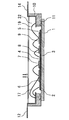
- FIG. 1 is a top view showing a semiconductor module according to the first embodiment.
- FIG. 2 is a cross-sectional view showing a semiconductor module according to the first embodiment.
- the material of the base plate 1 is copper or aluminum.
- An insulating substrate 2 is provided on the base plate 1.
- the material of the insulating substrate 2 is a ceramic plate such as silicon nitride, aluminum nitride, aluminum oxide, or Zr-containing alumina.
- silicon nitride and aluminum nitride are preferable from the viewpoint of thermal conductivity, and silicon nitride is more preferable from the viewpoint of material strength.
- Epoxy resin or the like may be used as the insulating substrate 2.
- a metal layer 3 is provided on the lower surface of the insulating substrate 2.
- the metal layer 3 is joined to the base plate 1 by solder or the like.
- Conductive patterns 4 and 5 are provided on the insulating substrate 2.
- the material of the metal layer 3 and the conductive patterns 4 and 5 is aluminum, an aluminum alloy, copper, or a copper alloy. In particular, copper having excellent electrical conductivity and thermal conductivity is preferable.
- Semiconductor elements 6 and 7 are provided on the conductive pattern 4.
- the bottom electrodes of the semiconductor elements 6 and 7 are joined to the conductive pattern 4 by solder or the like.
- Semiconductor elements 8 and 9 are provided on the conductive pattern 5.
- the bottom electrodes of the semiconductor elements 8 and 9 are joined to the conductive pattern 5 by solder or the like.
- the semiconductor elements 6 and 9 are switching elements such as MOSFETs or IGBTs that control a large current.
- the semiconductor elements 7 and 8 are freewheeling diodes.
- a square frame-shaped case 10 is arranged on the base plate 1 so as to surround the insulating substrate 2 and the semiconductor elements 6 to 9, and is bonded to the outer peripheral portion of the upper surface of the base plate 1 with an adhesive 11.
- the case 10 is required to maintain the insulating property without causing thermal deformation within the operating temperature range of the semiconductor module. Therefore, the material of the case 10 is a resin having a high softening point, such as PPS (PolyPhenylene Sulfide) resin and PBT (Polybutylene terephthalate) resin.
- the material of the adhesive 11 is, for example, a silicone resin, an epoxy resin, or the like. For example, the adhesive 11 is applied to the outer peripheral portion of the upper surface of the base plate 1, the case 10 is bonded to the base plate 1, and then the adhesive 11 is thermoset to perform the adhesion.
- the case 10 is provided with main terminals 12 to 14 and control terminals 15 and 16.
- the bonding wire 17 connects the top electrodes of the semiconductor elements 6 and 7 to the main terminal 12.
- the bonding wire 18 connects the conductive pattern 5 and the main terminal 13.
- the bonding wire 19 connects the conductive pattern 4, the top electrodes of the semiconductor elements 8 and 9, and the main terminal 14.
- the bonding wire 20 connects the control electrode of the semiconductor element 6 and the control terminal 15.
- the bonding wire 21 connects the control electrode of the semiconductor element 9 and the control terminal 16.
- the sealing material 22 seals the insulating substrate 2, the semiconductor elements 6 to 9, and the bonding wires 17 to 21 inside the case 10.
- the sealing material 22 is sealed by the base plate 1 and the case 10.
- the sealing material 22 is an epoxy resin, a phenol resin, a polyimide resin, or the like, and an inorganic filler having excellent thermal conductivity such as alumina or silica is added. Even when the adhesive 11 and the sealing material 22 are similar materials, they do not have the same coefficient of linear expansion because the additives differ depending on the application. Therefore, the heat cycle may generate thermal stress due to the difference in the coefficient of linear expansion.
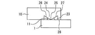
- FIG. 3 is an enlarged cross-sectional view of the joint portion between the case and the base plate of the semiconductor module according to the first embodiment.
- a groove 23 is provided on the lower surface of the case 10 facing the outer peripheral portion of the upper surface of the base plate 1.
- the bottom surface of the groove 23 has a protruding portion 24 protruding toward the base plate 1.
- the protrusion 24 has an apex 25 and gradients 26 and 27 provided on the inner side and the outer side of the case 10 with the apex 25 in between.
- the adhesive 11 is in contact with the apex 25 and is housed inside the groove 23.
- the width of the groove 23 is, for example, 2.6 mm or more, and is set according to the coating width and the positional variation of the adhesive 11.
- the depth of the groove 23 is, for example, 0.4 mm or more, and is set to the assumed value of the height of the adhesive 11 + 0.1 mm or more.
- the distance between the apex 25 of the protrusion 24 and the base plate 1 is, for example, 0 mm or more and 0.3 mm or less.
- the lower limit value is 0 mm
- the apex 25 comes into contact with the base plate 1.
- the upper limit value of 0.3 mm is lower than the assumed value of the height of the adhesive 11. The closer to the lower limit value, the easier it is for the apex 25 to come into contact with the adhesive 11.
- the lower surface of the case 10 has a flat surface 28 closer to the inside of the case 10 than the groove 23.
- the height of the protrusion 24 does not fall below the height position of the plane 28, and is equal to or less than the height at which the apex 25 contacts the base plate 1. Therefore, the flat surface 28 comes into surface contact with the outer peripheral portion of the upper surface of the base plate 1. As a result, even if the adhesive 11 protrudes from the groove 23, it is possible to prevent the adhesive 11 from invading the inside of the case 10. Further, it is possible to prevent the sealing material 22 from flowing out to the outside of the case 10.
- FIG. 4 is a bottom view showing the case according to the first embodiment.
- the groove 23 is provided on the entire circumference of the lower surface of the case 10. As described above, the groove 23 is preferably provided on the entire circumference of the region to which the adhesive 11 is applied, but may be provided only in a part thereof as long as the reliability can be ensured.
- FIG. 5 is a bottom view showing a modified example 1 of the case according to the first embodiment.
- a groove 23 having a protruding portion 24 is provided at a wide portion of the case 10.
- a groove 29 having no protruding portion 24 and a rectangular cross section is provided in a portion where the width of the case 10 is narrow.
- the groove 23 may be provided only in a place where a groove structure having a sufficient size can be provided.
- FIG. 6 is a bottom view showing a modified example 2 of the case according to the first embodiment.
- the case 10 is generally manufactured by injection molding. Therefore, in the case 10, the gate mark of the resin injection path and the ejector pin mark when taken out from the mold remain in the finished product. Therefore, the groove 23 is provided so as to avoid the region 30 where the gate mark or the ejector pin mark of the case 10 remains.
- FIG. 7 to 9 are cross-sectional views showing a step of joining the case of the semiconductor module according to the first embodiment to the base plate.
- the adhesive 11 is applied to the outer peripheral portion of the upper surface of the base plate 1.
- the adhesive 11 comes into contact with the apex 25 of the protrusion 24.
- the adhesive 11 is crushed and spreads along the gradients 26 and 27 of the protrusions 24. Thereby, a sufficient adhesive area can be secured.
- the case 10 and the base plate 1 can be joined regardless of the thickness of the adhesive 11.
- FIG. 10 is a cross-sectional view showing the relationship between the groove of the first embodiment and the comparative example and the adhesive application position.
- the gradients 26 and 27 are provided on both sides of the apex 25 of the protrusion 24, whereas in the comparative example, only one gradient 31 is provided. Therefore, in the comparative example, if the adhesive 11 is applied closer to the inside of the case 10 than the apex 25, the adhesive cannot be joined. Therefore, the margin W2 is small with respect to the variation in the coating position of the adhesive 11.
- the adhesive 11 comes into contact with the apex 25 of the protruding portion 24 and is crushed to both sides of the protruding portion 24. It spreads along the gradients 26 and 27. Therefore, even if the adhesive 11 is applied to the inner side or the outer side of the case 10 with respect to the apex 25, the bonding is possible. Therefore, the margin W1 can be increased with respect to the variation in the coating position of the adhesive 11. As a result, assembly defects can be reduced. Further, since the crushed adhesive 11 escapes to the excess space of the groove 23, the adhesive 11 is housed inside the groove 23 and does not penetrate to the inside of the case 10. Therefore, the interface between the adhesive 11 and the sealing material 22 can be eliminated or reduced, and the thermal cycle resistance can be improved.
- the gradients 26 and 27 and the base plate 1 can be adhered by the adhesive 11 if there is a slight deviation. Considering such a case, the margin for variation in the coating position of the adhesive 11 can be further increased.
- the adhesive 11 comes into contact with the apex 25 of the protrusion 24 and the gradients 26 and 27 in the vicinity thereof, not on the flat surface of the case 10. Therefore, since the amount of the adhesive 11 crushed is small, the adhesive 11 does not easily protrude from the joint.
- the case 10 cannot be joined to the base plate 1 by the adhesive 11.
- Increasing the amount of the adhesive 11 in order to increase the height of the adhesive 11 increases the risk of the adhesive 11 sticking out.
- the adhesive 11 can be joined even if the amount is small and the height is low. Is. Therefore, there is a margin for variations in the height of the adhesive 11.
- a conductive frame may be used instead of the bonding wires 17 to 21. This increases the allowable current capacity of the semiconductor module. Further, although it is assumed that the semiconductor module is used by connecting the base plate to the cooling fins via grease, pin fins may be formed on the base plate 1 instead of the cooling fins and grease. As a result, the assembly process can be omitted and the thermal resistance is improved.
- FIG. 11 is an enlarged cross-sectional view of the joint portion between the case and the base plate of the semiconductor module according to the second embodiment.
- the cross section of the protruding portion 24 provided on the bottom surface of the groove 23 of the case 10 is triangular, but in the present embodiment, the protruding portion 24 has a curved surface shape having a predetermined curvature.
- FIG. 12 is an enlarged cross-sectional view of the joint portion between the case and the base plate of the semiconductor module according to the third embodiment.
- the surface roughening process 32 is applied to the entire surface or part of the inner surface of the groove 23 of the case 10 and the entire surface or part of the area to which the adhesive 11 of the base plate 1 is applied.
- a fine uneven shape is formed on the surface by the surface roughening process 32.
- the height difference of the uneven shape is, for example, 0.01 mm or more.
- the flow length of the adhesive 11 becomes long, and the flow of the adhesive 11 is suppressed. Therefore, it becomes more difficult for the adhesive 11 to penetrate the inside of the case 10. Therefore, the interface between the adhesive 11 and the sealing material 22 can be eliminated or further reduced.
- Other configurations and effects are the same as those in the first embodiment.
- FIG. 13 is an enlarged cross-sectional view of the joint portion between the case and the base plate of the semiconductor module according to the fourth embodiment.
- a grid-like sheet 33 is attached to the entire surface or a part of the area of the base plate 1 to which the adhesive 11 is applied.
- the same effect as that of the third embodiment can be obtained.
- Other configurations and effects are the same as those in the first embodiment.
- FIG. 14 is an enlarged cross-sectional view of the joint portion between the case and the base plate of the semiconductor module according to the fifth embodiment.
- the bonding wire 34 is provided in the outer peripheral portion of the upper surface of the base plate 1 facing the groove 23 and in the region inside the case 10 with respect to the region where the adhesive 11 is applied. As a result, the same effect as that of the third embodiment can be obtained. Other configurations and effects are the same as those in the first embodiment.
- the bonding wire 34 may be provided in a region outside the case 10 as well as a region to which the adhesive 11 is applied. As a result, the adhesive 11 can be prevented from protruding to the outside of the case 10.
- FIG. 15 is an enlarged cross-sectional view of the joint portion between the case and the base plate of the semiconductor module according to the sixth embodiment.
- a recess 35 is provided in the base plate 1 so as to face the groove 23 of the case 10.
- the adhesive 11 is applied to the bottom surface of the recess 35.
- the width of the recess 35 is wider than the width of the area to which the adhesive 11 is applied and narrower than the width of the groove 23.
- the height of the protrusion 24 is set to a height at which the apex 25 comes into contact with the adhesive 11 in the recess 35.
- the depth of the recess 35 is, for example, 0.1 mm or more, but it is set to 4/5 or less of the thickness of the base plate 1 in order to prevent the base plate 1 from penetrating.
- the storage space for the adhesive 11 is widened. Therefore, it becomes more difficult for the adhesive 11 to penetrate the inside of the case 10. Therefore, the interface between the adhesive 11 and the sealing material 22 can be eliminated or further reduced.
- Other configurations and effects are the same as those in the first embodiment.
- FIG. 16 is an enlarged cross-sectional view of the joint portion between the case and the base plate of the semiconductor module according to the seventh embodiment.
- a recess 36 is provided on the outer peripheral portion of the upper surface of the base plate 1 in a region facing the lower surface of the case 10.
- the recess 36 is provided in a region inside the case 10 with respect to the region where the adhesive 11 is applied.
- the depth of the recess 36 is, for example, 1/10 or more of the thickness of the base plate 1, but is set to 4/5 or less of the thickness of the base plate 1 in order to prevent penetration of the base plate 1.
- the adhesive 11 crushed by the base plate 1 and the case 10 is housed in the recess 36. Therefore, it becomes more difficult for the adhesive 11 to penetrate the inside of the case 10. Therefore, the interface between the adhesive 11 and the sealing material 22 can be eliminated or further reduced.
- Other configurations and effects are the same as those in the first embodiment.
- FIG. 17 is a cross-sectional view showing a modification 1 of the seventh embodiment.
- a plurality of continuous recesses 36 may be provided as in the first modification.
- FIG. 18 is a cross-sectional view showing a modification 2 of the seventh embodiment.
- a plurality of recesses 36 may be provided in the areas closer to the inside and the outside of the case 10 than the area to which the adhesive 11 is applied as in the second modification. As a result, the adhesive 11 can be prevented from protruding to the outside of the case 10.
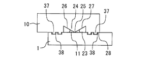
- FIG. 19 is an enlarged cross-sectional view of the joint portion between the case and the base plate of the semiconductor module according to the eighth embodiment.
- the outer peripheral portion of the upper surface of the base plate 1 and the lower surface of the case 10 come into contact with each other in a region closer to the inside of the case 10 than the groove 23.
- a concave portion 38 is provided on the outer peripheral portion of the upper surface of the base plate 1, and a convex portion 37 is provided on the lower surface of the case 10.
- the concave portion 38 has a size for accommodating the convex portion 37.
- the depth of the concave portion 38 and the height of the convex portion 37 are, for example, 1/10 or more of the thickness of the base plate 1. In order to prevent the base plate 1 from penetrating, the depth of the recess 38 is set to 4/5 or less of the thickness of the base plate 1.
- the adhesive 11 is closer to the inside of the case 10 than the predetermined position due to assembly variation, or if the amount of the adhesive 11 applied is large, the adhesive 11 spreads and reaches the contact area between the base plate 1 surface and the case 10. There is a problem that the adhesive 11 invades the inside of the case 10 due to the capillary phenomenon.
- the flow length of the adhesive 11 is increased by providing the convex portion 37 and the concave portion 38, it is possible to suppress the invasion of the adhesive 11 into the inside of the case 10. Therefore, the margin can be further increased with respect to the coating variation of the adhesive 11.
- FIG. 20 is a cross-sectional view showing a modification 1 of the eighth embodiment.
- a convex portion 37 is provided on the outer peripheral portion of the upper surface of the base plate 1
- a concave portion 38 is provided on the lower surface of the case 10. Even in this case, the same effect as that of the eighth embodiment can be obtained.
- FIG. 21 is a cross-sectional view showing a modification 2 of the eighth embodiment.
- a plurality of convex portions 37 and concave portions 38 are provided. This makes it more difficult for the adhesive 11 to penetrate the inside of the case 10.
- a convex portion 37 and a concave portion 38 are also provided in a contact region where the outer peripheral portion of the upper surface of the base plate 1 and the lower surface of the case 10 come into contact with each other on the outside of the case 10 than the groove 23. As a result, the adhesive 11 can be prevented from protruding to the outside of the case 10.
- FIG. 22 is a cross-sectional view showing a modification 3 of the eighth embodiment.
- a plurality of convex portions 37 are provided on the outer peripheral portion of the upper surface of the base plate 1, and a plurality of concave portions 38 are provided on the lower surface of the case 10. Even in this case, the same effect as that of the second modification can be obtained.
- FIG. 23 is a cross-sectional view showing the semiconductor module according to the ninth embodiment.
- FIG. 24 is an enlarged cross-sectional view of the joint portion between the case and the base plate of the semiconductor module according to the ninth embodiment.
- the upper surface of the base plate 1 is provided with a recess 39 closer to the inside than the outer peripheral portion of the upper surface to which the case 10 is joined.
- the insulating substrate 2 and the semiconductor elements 6 to 9 are provided in the recess 39.
- a convex portion 40 is provided closer to the inside of the case 10 than the groove 23 on the lower surface of the case 10.
- the convex portion 40 projects downward with respect to a portion outside the groove 23 on the lower surface of the case 10, and is inserted into the concave portion 39.
- the adhesive 11 that has been crushed and spread by joining the base plate 1 and the case 10 flows inward of the case 10, but is blocked by the convex portion 40. This makes it difficult for the adhesive 11 to penetrate the inside of the case 10. Therefore, the interface between the adhesive 11 and the sealing material 22 can be eliminated or reduced.
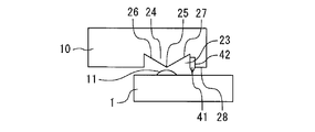
- Embodiment 10. 25 and 26 are enlarged cross-sectional views of the joint portion between the case and the base plate of the semiconductor module according to the tenth embodiment.
- FIG. 25 shows a state before joining the case 10 to the base plate 1
- FIG. 26 shows a state after joining.
- a protrusion 41 is provided on the lower surface of the case 10.
- the protrusion 41 is provided closer to the inside of the case 10 than the groove 23.
- the height of the protrusion 41 is, for example, 1/10 or more of the thickness of the base plate 1 and 1/2 or less of the thickness of the base plate 1.
- FIG. 27 and 28 are cross-sectional views showing a modification 1 of the tenth embodiment.
- FIG. 27 shows a state before joining the case 10 to the base plate 1
- FIG. 28 shows a state after joining.
- a high-strength material such as copper is used for the base plate 1, and the base plate 1 is provided with protrusions 41.
- the lower surface of the case 10 comes into contact with the protrusion 41 and buckles due to surface pressure to join the base plate 1 and the case 10. Even in this case, the same effect as that of the tenth embodiment can be obtained.
- FIG. 29 is a cross-sectional view showing a modification 2 of the tenth embodiment.
- the protrusion 41 is a metal 42 inserted into the lower surface of the case 10.
- the metal 42 has a higher strength than the base plate 1. As a result, buckling of the base plate 1 is likely to occur, and the base plate 1 and the case 10 are easily joined.
- a metal 42 may be inserted into the outer peripheral portion of the upper surface of the base plate 1 to provide a protrusion 41.
- the semiconductor elements 6 to 9 are not limited to those formed of silicon, and may be formed of a wide bandgap semiconductor having a larger bandgap than silicon.
- the wide bandgap semiconductor is, for example, silicon carbide, gallium nitride based material, or diamond.
- a power semiconductor device formed of such a wide bandgap semiconductor has high withstand voltage resistance and allowable current density, and thus can be miniaturized.
- the semiconductor module incorporating this element can also be miniaturized.
- the heat resistance of the element is high, the heat radiation fins of the heat sink can be miniaturized, and the water-cooled portion can be air-cooled, so that the semiconductor module can be further miniaturized.
Landscapes
- Structures Or Materials For Encapsulating Or Coating Semiconductor Devices Or Solid State Devices (AREA)
- Cooling Or The Like Of Semiconductors Or Solid State Devices (AREA)
Priority Applications (5)
| Application Number | Priority Date | Filing Date | Title |
|---|---|---|---|
| PCT/JP2019/046445 WO2021106114A1 (ja) | 2019-11-27 | 2019-11-27 | 半導体モジュール |
| CN201980102435.8A CN114730745B (zh) | 2019-11-27 | 2019-11-27 | 半导体模块 |
| US17/627,171 US12131969B2 (en) | 2019-11-27 | 2019-11-27 | Semiconductor module |
| DE112019007915.8T DE112019007915T5 (de) | 2019-11-27 | 2019-11-27 | Halbleitermodul |
| JP2021560830A JP7173375B2 (ja) | 2019-11-27 | 2019-11-27 | 半導体モジュール |
Applications Claiming Priority (1)
| Application Number | Priority Date | Filing Date | Title |
|---|---|---|---|
| PCT/JP2019/046445 WO2021106114A1 (ja) | 2019-11-27 | 2019-11-27 | 半導体モジュール |
Publications (1)
| Publication Number | Publication Date |
|---|---|
| WO2021106114A1 true WO2021106114A1 (ja) | 2021-06-03 |
Family
ID=76128686
Family Applications (1)
| Application Number | Title | Priority Date | Filing Date |
|---|---|---|---|
| PCT/JP2019/046445 Ceased WO2021106114A1 (ja) | 2019-11-27 | 2019-11-27 | 半導体モジュール |
Country Status (5)
| Country | Link |
|---|---|
| US (1) | US12131969B2 (https=) |
| JP (1) | JP7173375B2 (https=) |
| CN (1) | CN114730745B (https=) |
| DE (1) | DE112019007915T5 (https=) |
| WO (1) | WO2021106114A1 (https=) |
Cited By (3)
| Publication number | Priority date | Publication date | Assignee | Title |
|---|---|---|---|---|
| JP2021150575A (ja) * | 2020-03-23 | 2021-09-27 | 株式会社東芝 | 半導体装置 |
| CN115602635A (zh) * | 2021-07-07 | 2023-01-13 | 三菱电机株式会社(Jp) | 半导体装置及逆变器装置 |
| WO2024190589A1 (ja) * | 2023-03-14 | 2024-09-19 | 新電元工業株式会社 | 半導体モジュール |
Families Citing this family (1)
| Publication number | Priority date | Publication date | Assignee | Title |
|---|---|---|---|---|
| CN116711072A (zh) * | 2021-01-22 | 2023-09-05 | 三菱电机株式会社 | 半导体装置及半导体装置的制造方法 |
Citations (13)
| Publication number | Priority date | Publication date | Assignee | Title |
|---|---|---|---|---|
| JPS553617A (en) * | 1978-06-21 | 1980-01-11 | Hitachi Ltd | Metallic base for hybrid integrated circuit |
| JPS61139048A (ja) * | 1984-12-11 | 1986-06-26 | Toshiba Corp | 半導体装置 |
| JPS63100842U (https=) * | 1986-12-19 | 1988-06-30 | ||
| JPS6417455A (en) * | 1987-07-10 | 1989-01-20 | Mitsubishi Electric Corp | Semiconductor device |
| JPH06268102A (ja) * | 1993-01-13 | 1994-09-22 | Fuji Electric Co Ltd | 樹脂封止形半導体装置 |
| JP2000323593A (ja) * | 1999-05-06 | 2000-11-24 | Yazaki Corp | 半導体装置 |
| JP2004103846A (ja) * | 2002-09-10 | 2004-04-02 | Mitsubishi Electric Corp | 電力用半導体装置 |
| JP2005322784A (ja) * | 2004-05-10 | 2005-11-17 | Mitsubishi Electric Corp | 電力用半導体装置 |
| JP2012015349A (ja) * | 2010-07-01 | 2012-01-19 | Fuji Electric Co Ltd | 半導体装置 |
| WO2017098593A1 (ja) * | 2015-12-09 | 2017-06-15 | 三菱電機株式会社 | パワーモジュール |
| WO2018055667A1 (ja) * | 2016-09-20 | 2018-03-29 | 三菱電機株式会社 | 半導体装置 |
| WO2019049400A1 (ja) * | 2017-09-05 | 2019-03-14 | 三菱電機株式会社 | パワーモジュール及びその製造方法並びに電力変換装置 |
| JP2019096797A (ja) * | 2017-11-27 | 2019-06-20 | 三菱電機株式会社 | 半導体装置および電力変換装置 |
Family Cites Families (4)
| Publication number | Priority date | Publication date | Assignee | Title |
|---|---|---|---|---|
| JP4335263B2 (ja) * | 2007-02-07 | 2009-09-30 | ソニー株式会社 | 半導体装置および半導体装置の製造方法 |
| JP5842929B2 (ja) * | 2011-11-22 | 2016-01-13 | 富士通株式会社 | 電子部品およびその製造方法 |
| JP5968611B2 (ja) * | 2011-11-22 | 2016-08-10 | 新電元工業株式会社 | パワーモジュールおよびその製造方法、並びに樹脂フレーム |
| JP6399272B1 (ja) | 2017-09-05 | 2018-10-03 | 三菱電機株式会社 | パワーモジュール及びその製造方法並びに電力変換装置 |
-
2019
- 2019-11-27 DE DE112019007915.8T patent/DE112019007915T5/de active Pending
- 2019-11-27 JP JP2021560830A patent/JP7173375B2/ja active Active
- 2019-11-27 US US17/627,171 patent/US12131969B2/en active Active
- 2019-11-27 CN CN201980102435.8A patent/CN114730745B/zh active Active
- 2019-11-27 WO PCT/JP2019/046445 patent/WO2021106114A1/ja not_active Ceased
Patent Citations (13)
| Publication number | Priority date | Publication date | Assignee | Title |
|---|---|---|---|---|
| JPS553617A (en) * | 1978-06-21 | 1980-01-11 | Hitachi Ltd | Metallic base for hybrid integrated circuit |
| JPS61139048A (ja) * | 1984-12-11 | 1986-06-26 | Toshiba Corp | 半導体装置 |
| JPS63100842U (https=) * | 1986-12-19 | 1988-06-30 | ||
| JPS6417455A (en) * | 1987-07-10 | 1989-01-20 | Mitsubishi Electric Corp | Semiconductor device |
| JPH06268102A (ja) * | 1993-01-13 | 1994-09-22 | Fuji Electric Co Ltd | 樹脂封止形半導体装置 |
| JP2000323593A (ja) * | 1999-05-06 | 2000-11-24 | Yazaki Corp | 半導体装置 |
| JP2004103846A (ja) * | 2002-09-10 | 2004-04-02 | Mitsubishi Electric Corp | 電力用半導体装置 |
| JP2005322784A (ja) * | 2004-05-10 | 2005-11-17 | Mitsubishi Electric Corp | 電力用半導体装置 |
| JP2012015349A (ja) * | 2010-07-01 | 2012-01-19 | Fuji Electric Co Ltd | 半導体装置 |
| WO2017098593A1 (ja) * | 2015-12-09 | 2017-06-15 | 三菱電機株式会社 | パワーモジュール |
| WO2018055667A1 (ja) * | 2016-09-20 | 2018-03-29 | 三菱電機株式会社 | 半導体装置 |
| WO2019049400A1 (ja) * | 2017-09-05 | 2019-03-14 | 三菱電機株式会社 | パワーモジュール及びその製造方法並びに電力変換装置 |
| JP2019096797A (ja) * | 2017-11-27 | 2019-06-20 | 三菱電機株式会社 | 半導体装置および電力変換装置 |
Cited By (6)
| Publication number | Priority date | Publication date | Assignee | Title |
|---|---|---|---|---|
| JP2021150575A (ja) * | 2020-03-23 | 2021-09-27 | 株式会社東芝 | 半導体装置 |
| JP7258806B2 (ja) | 2020-03-23 | 2023-04-17 | 株式会社東芝 | 半導体装置 |
| CN115602635A (zh) * | 2021-07-07 | 2023-01-13 | 三菱电机株式会社(Jp) | 半导体装置及逆变器装置 |
| JP2023009601A (ja) * | 2021-07-07 | 2023-01-20 | 三菱電機株式会社 | 半導体装置及びインバータ装置 |
| JP7637852B2 (ja) | 2021-07-07 | 2025-03-03 | 三菱電機株式会社 | 半導体装置及びインバータ装置 |
| WO2024190589A1 (ja) * | 2023-03-14 | 2024-09-19 | 新電元工業株式会社 | 半導体モジュール |
Also Published As
| Publication number | Publication date |
|---|---|
| US20220278004A1 (en) | 2022-09-01 |
| JP7173375B2 (ja) | 2022-11-16 |
| JPWO2021106114A1 (https=) | 2021-06-03 |
| CN114730745A (zh) | 2022-07-08 |
| US12131969B2 (en) | 2024-10-29 |
| CN114730745B (zh) | 2025-09-05 |
| DE112019007915T5 (de) | 2022-09-08 |
Similar Documents
| Publication | Publication Date | Title |
|---|---|---|
| JP4455488B2 (ja) | 半導体装置 | |
| US7728413B2 (en) | Resin mold type semiconductor device | |
| US11201121B2 (en) | Semiconductor device | |
| US6734551B2 (en) | Semiconductor device | |
| JP7173375B2 (ja) | 半導体モジュール | |
| CN111341731B (zh) | 半导体装置 | |
| WO2013118478A1 (ja) | 半導体装置 | |
| JP2014216459A (ja) | 半導体装置 | |
| CN112236855B (zh) | 半导体装置 | |
| US12100631B2 (en) | Semiconductor device | |
| JP2005191071A (ja) | 半導体装置 | |
| US20210257269A1 (en) | Semiconductor device | |
| CN112530915A (zh) | 半导体装置 | |
| CN105633024A (zh) | 半导体装置 | |
| JP7494521B2 (ja) | 半導体装置及び半導体装置の製造方法 | |
| JP2020072101A (ja) | パワーユニット、パワーユニットの製造方法、パワーユニットを有する電気装置及びヒートシンク | |
| US20230282541A1 (en) | Semiconductor device | |
| US20230215776A1 (en) | Semiconductor device | |
| CN114203650A (zh) | 半导体装置和半导体装置的制造方法 | |
| CN108630620B (zh) | 半导体装置 | |
| CN115206905A (zh) | 半导体装置和使用该半导体装置的半导体模块 | |
| US20240266265A1 (en) | Semiconductor device | |
| US20240304567A1 (en) | Semiconductor device and method of manufacturing semiconductor device | |
| US20260060135A1 (en) | Semiconductor device | |
| JP7634456B2 (ja) | 半導体装置 |
Legal Events
| Date | Code | Title | Description |
|---|---|---|---|
| 121 | Ep: the epo has been informed by wipo that ep was designated in this application |
Ref document number: 19954282 Country of ref document: EP Kind code of ref document: A1 |
|
| ENP | Entry into the national phase |
Ref document number: 2021560830 Country of ref document: JP Kind code of ref document: A |
|
| 122 | Ep: pct application non-entry in european phase |
Ref document number: 19954282 Country of ref document: EP Kind code of ref document: A1 |
|
| WWG | Wipo information: grant in national office |
Ref document number: 201980102435.8 Country of ref document: CN |