WO2021106114A1 - Semiconductor module - Google Patents
Semiconductor module Download PDFInfo
- Publication number
- WO2021106114A1 WO2021106114A1 PCT/JP2019/046445 JP2019046445W WO2021106114A1 WO 2021106114 A1 WO2021106114 A1 WO 2021106114A1 JP 2019046445 W JP2019046445 W JP 2019046445W WO 2021106114 A1 WO2021106114 A1 WO 2021106114A1
- Authority
- WO
- WIPO (PCT)
- Prior art keywords
- case
- base plate
- adhesive
- semiconductor module
- module according
- Prior art date
Links
Images


Classifications
-
- H—ELECTRICITY
- H01—ELECTRIC ELEMENTS
- H01L—SEMICONDUCTOR DEVICES NOT COVERED BY CLASS H10
- H01L25/00—Assemblies consisting of a plurality of individual semiconductor or other solid state devices ; Multistep manufacturing processes thereof
- H01L25/03—Assemblies consisting of a plurality of individual semiconductor or other solid state devices ; Multistep manufacturing processes thereof all the devices being of a type provided for in the same subgroup of groups H01L27/00 - H01L33/00, or in a single subclass of H10K, H10N, e.g. assemblies of rectifier diodes
- H01L25/04—Assemblies consisting of a plurality of individual semiconductor or other solid state devices ; Multistep manufacturing processes thereof all the devices being of a type provided for in the same subgroup of groups H01L27/00 - H01L33/00, or in a single subclass of H10K, H10N, e.g. assemblies of rectifier diodes the devices not having separate containers
- H01L25/07—Assemblies consisting of a plurality of individual semiconductor or other solid state devices ; Multistep manufacturing processes thereof all the devices being of a type provided for in the same subgroup of groups H01L27/00 - H01L33/00, or in a single subclass of H10K, H10N, e.g. assemblies of rectifier diodes the devices not having separate containers the devices being of a type provided for in group H01L29/00
- H01L25/072—Assemblies consisting of a plurality of individual semiconductor or other solid state devices ; Multistep manufacturing processes thereof all the devices being of a type provided for in the same subgroup of groups H01L27/00 - H01L33/00, or in a single subclass of H10K, H10N, e.g. assemblies of rectifier diodes the devices not having separate containers the devices being of a type provided for in group H01L29/00 the devices being arranged next to each other
-
- H—ELECTRICITY
- H01—ELECTRIC ELEMENTS
- H01L—SEMICONDUCTOR DEVICES NOT COVERED BY CLASS H10
- H01L23/00—Details of semiconductor or other solid state devices
- H01L23/02—Containers; Seals
- H01L23/04—Containers; Seals characterised by the shape of the container or parts, e.g. caps, walls
- H01L23/043—Containers; Seals characterised by the shape of the container or parts, e.g. caps, walls the container being a hollow construction and having a conductive base as a mounting as well as a lead for the semiconductor body
- H01L23/047—Containers; Seals characterised by the shape of the container or parts, e.g. caps, walls the container being a hollow construction and having a conductive base as a mounting as well as a lead for the semiconductor body the other leads being parallel to the base
-
- H—ELECTRICITY
- H01—ELECTRIC ELEMENTS
- H01L—SEMICONDUCTOR DEVICES NOT COVERED BY CLASS H10
- H01L23/00—Details of semiconductor or other solid state devices
- H01L23/02—Containers; Seals
- H01L23/10—Containers; Seals characterised by the material or arrangement of seals between parts, e.g. between cap and base of the container or between leads and walls of the container
-
- H—ELECTRICITY
- H01—ELECTRIC ELEMENTS
- H01L—SEMICONDUCTOR DEVICES NOT COVERED BY CLASS H10
- H01L23/00—Details of semiconductor or other solid state devices
- H01L23/34—Arrangements for cooling, heating, ventilating or temperature compensation ; Temperature sensing arrangements
-
- H—ELECTRICITY
- H01—ELECTRIC ELEMENTS
- H01L—SEMICONDUCTOR DEVICES NOT COVERED BY CLASS H10
- H01L25/00—Assemblies consisting of a plurality of individual semiconductor or other solid state devices ; Multistep manufacturing processes thereof
- H01L25/03—Assemblies consisting of a plurality of individual semiconductor or other solid state devices ; Multistep manufacturing processes thereof all the devices being of a type provided for in the same subgroup of groups H01L27/00 - H01L33/00, or in a single subclass of H10K, H10N, e.g. assemblies of rectifier diodes
- H01L25/04—Assemblies consisting of a plurality of individual semiconductor or other solid state devices ; Multistep manufacturing processes thereof all the devices being of a type provided for in the same subgroup of groups H01L27/00 - H01L33/00, or in a single subclass of H10K, H10N, e.g. assemblies of rectifier diodes the devices not having separate containers
- H01L25/07—Assemblies consisting of a plurality of individual semiconductor or other solid state devices ; Multistep manufacturing processes thereof all the devices being of a type provided for in the same subgroup of groups H01L27/00 - H01L33/00, or in a single subclass of H10K, H10N, e.g. assemblies of rectifier diodes the devices not having separate containers the devices being of a type provided for in group H01L29/00
-
- H—ELECTRICITY
- H01—ELECTRIC ELEMENTS
- H01L—SEMICONDUCTOR DEVICES NOT COVERED BY CLASS H10
- H01L25/00—Assemblies consisting of a plurality of individual semiconductor or other solid state devices ; Multistep manufacturing processes thereof
- H01L25/18—Assemblies consisting of a plurality of individual semiconductor or other solid state devices ; Multistep manufacturing processes thereof the devices being of types provided for in two or more different subgroups of the same main group of groups H01L27/00 - H01L33/00, or in a single subclass of H10K, H10N
-
- H—ELECTRICITY
- H01—ELECTRIC ELEMENTS
- H01L—SEMICONDUCTOR DEVICES NOT COVERED BY CLASS H10
- H01L2224/00—Indexing scheme for arrangements for connecting or disconnecting semiconductor or solid-state bodies and methods related thereto as covered by H01L24/00
- H01L2224/01—Means for bonding being attached to, or being formed on, the surface to be connected, e.g. chip-to-package, die-attach, "first-level" interconnects; Manufacturing methods related thereto
- H01L2224/42—Wire connectors; Manufacturing methods related thereto
- H01L2224/47—Structure, shape, material or disposition of the wire connectors after the connecting process
- H01L2224/48—Structure, shape, material or disposition of the wire connectors after the connecting process of an individual wire connector
- H01L2224/481—Disposition
- H01L2224/48135—Connecting between different semiconductor or solid-state bodies, i.e. chip-to-chip
- H01L2224/48137—Connecting between different semiconductor or solid-state bodies, i.e. chip-to-chip the bodies being arranged next to each other, e.g. on a common substrate
- H01L2224/48139—Connecting between different semiconductor or solid-state bodies, i.e. chip-to-chip the bodies being arranged next to each other, e.g. on a common substrate with an intermediate bond, e.g. continuous wire daisy chain
-
- H—ELECTRICITY
- H01—ELECTRIC ELEMENTS
- H01L—SEMICONDUCTOR DEVICES NOT COVERED BY CLASS H10
- H01L2224/00—Indexing scheme for arrangements for connecting or disconnecting semiconductor or solid-state bodies and methods related thereto as covered by H01L24/00
- H01L2224/01—Means for bonding being attached to, or being formed on, the surface to be connected, e.g. chip-to-package, die-attach, "first-level" interconnects; Manufacturing methods related thereto
- H01L2224/42—Wire connectors; Manufacturing methods related thereto
- H01L2224/47—Structure, shape, material or disposition of the wire connectors after the connecting process
- H01L2224/49—Structure, shape, material or disposition of the wire connectors after the connecting process of a plurality of wire connectors
- H01L2224/491—Disposition
- H01L2224/4911—Disposition the connectors being bonded to at least one common bonding area, e.g. daisy chain
- H01L2224/49111—Disposition the connectors being bonded to at least one common bonding area, e.g. daisy chain the connectors connecting two common bonding areas, e.g. Litz or braid wires
-
- H—ELECTRICITY
- H01—ELECTRIC ELEMENTS
- H01L—SEMICONDUCTOR DEVICES NOT COVERED BY CLASS H10
- H01L23/00—Details of semiconductor or other solid state devices
- H01L23/02—Containers; Seals
- H01L23/04—Containers; Seals characterised by the shape of the container or parts, e.g. caps, walls
- H01L23/053—Containers; Seals characterised by the shape of the container or parts, e.g. caps, walls the container being a hollow construction and having an insulating or insulated base as a mounting for the semiconductor body
-
- H—ELECTRICITY
- H01—ELECTRIC ELEMENTS
- H01L—SEMICONDUCTOR DEVICES NOT COVERED BY CLASS H10
- H01L2924/00—Indexing scheme for arrangements or methods for connecting or disconnecting semiconductor or solid-state bodies as covered by H01L24/00
- H01L2924/19—Details of hybrid assemblies other than the semiconductor or other solid state devices to be connected
- H01L2924/191—Disposition
- H01L2924/19101—Disposition of discrete passive components
- H01L2924/19107—Disposition of discrete passive components off-chip wires
Definitions
- the present invention relates to a semiconductor module.
- adhesives are generally used to join the case and base plate.
- MOSFETs Metal Oxide Semiconductor Field Effect Transistors
- IGBTs Insulated Gate Bipolar Transistors
- diodes adhesives are generally used to join the case and base plate.
- an interface between the adhesive and the sealing material is generated inside the case.
- the bonding strength between them is weak, so that the interface is likely to be peeled off due to thermal cycle stress. Therefore, there is a problem that the thermodynamic cycle endurance is lowered and the reliability is impaired.
- a structure has been proposed in which the case is provided with a slope to prevent the adhesive from entering the inside of the case (see, for example, Patent Document 1).
- the adhesive may penetrate too much inside the case after joining. Also, if the adhesive is located on the outside of the case, the case and base plate may not be sufficiently bonded.
- the present invention has been made to solve the above-mentioned problems, and an object of the present invention is to obtain a semiconductor module capable of improving the thermodynamic cycle resistance and increasing the margin with respect to the variation in the adhesive coating position. ..
- the semiconductor module according to the present invention is arranged so as to surround the base plate, the insulating substrate provided on the base plate, the semiconductor element provided on the insulating substrate, the insulating substrate, and the semiconductor element.
- the case is provided with a case bonded to the base plate with an adhesive, and a sealing material for sealing the insulating substrate and the semiconductor element inside the case, and faces the outer peripheral portion of the upper surface of the base plate.
- the lower surface of the groove is provided, and the bottom surface of the groove has a protruding portion protruding toward the base plate, and the protruding portion is located between the apex and the inner side and the outer side of the case with the apex in between.
- Each has a provided gradient, and the adhesive is in contact with the apex and is housed inside the groove.
- the adhesive comes into contact with the apex of the protruding portion.
- the adhesive is crushed and spreads along the slope of the protrusion. Thereby, a sufficient adhesive area can be secured.
- the case and the base plate can be joined regardless of the thickness of the adhesive.
- the margin can be increased with respect to the variation in the coating position of the adhesive.
- the crushed adhesive escapes to the excess space of the groove, the adhesive is contained inside the groove and does not penetrate to the inside of the case. Therefore, the interface between the adhesive and the sealing material can be eliminated or reduced, and the thermal cycle resistance can be improved.
- FIG. 5 is an enlarged cross-sectional view of a joint portion between a semiconductor module case and a base plate according to the first embodiment. It is a bottom view which shows the case which concerns on Embodiment 1. FIG. It is a bottom view which shows the modification 1 of the case which concerns on Embodiment 1. FIG. It is a bottom view which shows the modification 2 of the case which concerns on Embodiment 1. FIG. It is sectional drawing which shows the process of joining the case of the semiconductor module which concerns on Embodiment 1 to a base plate.
- FIG. 5 is an enlarged cross-sectional view of a joint portion between a semiconductor module case and a base plate according to a second embodiment.
- FIG. 5 is an enlarged cross-sectional view of a joint portion between a semiconductor module case and a base plate according to a third embodiment.
- FIG. 5 is an enlarged cross-sectional view of a joint portion between a semiconductor module case and a base plate according to a fourth embodiment.
- FIG. 5 is an enlarged cross-sectional view of a joint portion between a semiconductor module case and a base plate according to a fifth embodiment.
- FIG. 5 is an enlarged cross-sectional view of a joint portion between a semiconductor module case and a base plate according to a sixth embodiment.
- FIG. 5 is an enlarged cross-sectional view of a joint portion between a semiconductor module case and a base plate according to a seventh embodiment. It is sectional drawing which shows the modification 1 of Embodiment 7. It is sectional drawing which shows the modification 2 of Embodiment 7.
- FIG. 5 is an enlarged cross-sectional view of a joint portion between a semiconductor module case and a base plate according to the eighth embodiment. It is sectional drawing which shows the modification 1 of Embodiment 8. It is sectional drawing which shows the modification 2 of Embodiment 8. It is sectional drawing which shows the modification 3 of Embodiment 8. It is sectional drawing which shows the semiconductor module which concerns on Embodiment 9.
- FIG. 9 is an enlarged cross-sectional view of a joint portion between a semiconductor module case and a base plate according to a ninth embodiment.
- FIG. 5 is an enlarged cross-sectional view of a joint portion between a semiconductor module case and a base plate according to a tenth embodiment.
- FIG. 5 is an enlarged cross-sectional view of a joint portion between a semiconductor module case and a base plate according to a tenth embodiment. It is sectional drawing which shows the modification 1 of Embodiment 10. It is sectional drawing which shows the modification 1 of Embodiment 10. It is sectional drawing which shows the modification 2 of Embodiment 10.
- FIG. 1 is a top view showing a semiconductor module according to the first embodiment.
- FIG. 2 is a cross-sectional view showing a semiconductor module according to the first embodiment.
- the material of the base plate 1 is copper or aluminum.
- An insulating substrate 2 is provided on the base plate 1.
- the material of the insulating substrate 2 is a ceramic plate such as silicon nitride, aluminum nitride, aluminum oxide, or Zr-containing alumina.
- silicon nitride and aluminum nitride are preferable from the viewpoint of thermal conductivity, and silicon nitride is more preferable from the viewpoint of material strength.
- Epoxy resin or the like may be used as the insulating substrate 2.
- a metal layer 3 is provided on the lower surface of the insulating substrate 2.
- the metal layer 3 is joined to the base plate 1 by solder or the like.
- Conductive patterns 4 and 5 are provided on the insulating substrate 2.
- the material of the metal layer 3 and the conductive patterns 4 and 5 is aluminum, an aluminum alloy, copper, or a copper alloy. In particular, copper having excellent electrical conductivity and thermal conductivity is preferable.
- Semiconductor elements 6 and 7 are provided on the conductive pattern 4.
- the bottom electrodes of the semiconductor elements 6 and 7 are joined to the conductive pattern 4 by solder or the like.
- Semiconductor elements 8 and 9 are provided on the conductive pattern 5.
- the bottom electrodes of the semiconductor elements 8 and 9 are joined to the conductive pattern 5 by solder or the like.
- the semiconductor elements 6 and 9 are switching elements such as MOSFETs or IGBTs that control a large current.
- the semiconductor elements 7 and 8 are freewheeling diodes.
- a square frame-shaped case 10 is arranged on the base plate 1 so as to surround the insulating substrate 2 and the semiconductor elements 6 to 9, and is bonded to the outer peripheral portion of the upper surface of the base plate 1 with an adhesive 11.
- the case 10 is required to maintain the insulating property without causing thermal deformation within the operating temperature range of the semiconductor module. Therefore, the material of the case 10 is a resin having a high softening point, such as PPS (PolyPhenylene Sulfide) resin and PBT (Polybutylene terephthalate) resin.
- the material of the adhesive 11 is, for example, a silicone resin, an epoxy resin, or the like. For example, the adhesive 11 is applied to the outer peripheral portion of the upper surface of the base plate 1, the case 10 is bonded to the base plate 1, and then the adhesive 11 is thermoset to perform the adhesion.
- the case 10 is provided with main terminals 12 to 14 and control terminals 15 and 16.
- the bonding wire 17 connects the top electrodes of the semiconductor elements 6 and 7 to the main terminal 12.
- the bonding wire 18 connects the conductive pattern 5 and the main terminal 13.
- the bonding wire 19 connects the conductive pattern 4, the top electrodes of the semiconductor elements 8 and 9, and the main terminal 14.
- the bonding wire 20 connects the control electrode of the semiconductor element 6 and the control terminal 15.
- the bonding wire 21 connects the control electrode of the semiconductor element 9 and the control terminal 16.
- the sealing material 22 seals the insulating substrate 2, the semiconductor elements 6 to 9, and the bonding wires 17 to 21 inside the case 10.
- the sealing material 22 is sealed by the base plate 1 and the case 10.
- the sealing material 22 is an epoxy resin, a phenol resin, a polyimide resin, or the like, and an inorganic filler having excellent thermal conductivity such as alumina or silica is added. Even when the adhesive 11 and the sealing material 22 are similar materials, they do not have the same coefficient of linear expansion because the additives differ depending on the application. Therefore, the heat cycle may generate thermal stress due to the difference in the coefficient of linear expansion.
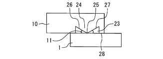
- FIG. 3 is an enlarged cross-sectional view of the joint portion between the case and the base plate of the semiconductor module according to the first embodiment.
- a groove 23 is provided on the lower surface of the case 10 facing the outer peripheral portion of the upper surface of the base plate 1.
- the bottom surface of the groove 23 has a protruding portion 24 protruding toward the base plate 1.
- the protrusion 24 has an apex 25 and gradients 26 and 27 provided on the inner side and the outer side of the case 10 with the apex 25 in between.
- the adhesive 11 is in contact with the apex 25 and is housed inside the groove 23.
- the width of the groove 23 is, for example, 2.6 mm or more, and is set according to the coating width and the positional variation of the adhesive 11.
- the depth of the groove 23 is, for example, 0.4 mm or more, and is set to the assumed value of the height of the adhesive 11 + 0.1 mm or more.
- the distance between the apex 25 of the protrusion 24 and the base plate 1 is, for example, 0 mm or more and 0.3 mm or less.
- the lower limit value is 0 mm
- the apex 25 comes into contact with the base plate 1.
- the upper limit value of 0.3 mm is lower than the assumed value of the height of the adhesive 11. The closer to the lower limit value, the easier it is for the apex 25 to come into contact with the adhesive 11.
- the lower surface of the case 10 has a flat surface 28 closer to the inside of the case 10 than the groove 23.
- the height of the protrusion 24 does not fall below the height position of the plane 28, and is equal to or less than the height at which the apex 25 contacts the base plate 1. Therefore, the flat surface 28 comes into surface contact with the outer peripheral portion of the upper surface of the base plate 1. As a result, even if the adhesive 11 protrudes from the groove 23, it is possible to prevent the adhesive 11 from invading the inside of the case 10. Further, it is possible to prevent the sealing material 22 from flowing out to the outside of the case 10.
- FIG. 4 is a bottom view showing the case according to the first embodiment.
- the groove 23 is provided on the entire circumference of the lower surface of the case 10. As described above, the groove 23 is preferably provided on the entire circumference of the region to which the adhesive 11 is applied, but may be provided only in a part thereof as long as the reliability can be ensured.
- FIG. 5 is a bottom view showing a modified example 1 of the case according to the first embodiment.
- a groove 23 having a protruding portion 24 is provided at a wide portion of the case 10.
- a groove 29 having no protruding portion 24 and a rectangular cross section is provided in a portion where the width of the case 10 is narrow.
- the groove 23 may be provided only in a place where a groove structure having a sufficient size can be provided.
- FIG. 6 is a bottom view showing a modified example 2 of the case according to the first embodiment.
- the case 10 is generally manufactured by injection molding. Therefore, in the case 10, the gate mark of the resin injection path and the ejector pin mark when taken out from the mold remain in the finished product. Therefore, the groove 23 is provided so as to avoid the region 30 where the gate mark or the ejector pin mark of the case 10 remains.
- FIG. 7 to 9 are cross-sectional views showing a step of joining the case of the semiconductor module according to the first embodiment to the base plate.
- the adhesive 11 is applied to the outer peripheral portion of the upper surface of the base plate 1.
- the adhesive 11 comes into contact with the apex 25 of the protrusion 24.
- the adhesive 11 is crushed and spreads along the gradients 26 and 27 of the protrusions 24. Thereby, a sufficient adhesive area can be secured.
- the case 10 and the base plate 1 can be joined regardless of the thickness of the adhesive 11.
- FIG. 10 is a cross-sectional view showing the relationship between the groove of the first embodiment and the comparative example and the adhesive application position.
- the gradients 26 and 27 are provided on both sides of the apex 25 of the protrusion 24, whereas in the comparative example, only one gradient 31 is provided. Therefore, in the comparative example, if the adhesive 11 is applied closer to the inside of the case 10 than the apex 25, the adhesive cannot be joined. Therefore, the margin W2 is small with respect to the variation in the coating position of the adhesive 11.
- the adhesive 11 comes into contact with the apex 25 of the protruding portion 24 and is crushed to both sides of the protruding portion 24. It spreads along the gradients 26 and 27. Therefore, even if the adhesive 11 is applied to the inner side or the outer side of the case 10 with respect to the apex 25, the bonding is possible. Therefore, the margin W1 can be increased with respect to the variation in the coating position of the adhesive 11. As a result, assembly defects can be reduced. Further, since the crushed adhesive 11 escapes to the excess space of the groove 23, the adhesive 11 is housed inside the groove 23 and does not penetrate to the inside of the case 10. Therefore, the interface between the adhesive 11 and the sealing material 22 can be eliminated or reduced, and the thermal cycle resistance can be improved.
- the gradients 26 and 27 and the base plate 1 can be adhered by the adhesive 11 if there is a slight deviation. Considering such a case, the margin for variation in the coating position of the adhesive 11 can be further increased.
- the adhesive 11 comes into contact with the apex 25 of the protrusion 24 and the gradients 26 and 27 in the vicinity thereof, not on the flat surface of the case 10. Therefore, since the amount of the adhesive 11 crushed is small, the adhesive 11 does not easily protrude from the joint.
- the case 10 cannot be joined to the base plate 1 by the adhesive 11.
- Increasing the amount of the adhesive 11 in order to increase the height of the adhesive 11 increases the risk of the adhesive 11 sticking out.
- the adhesive 11 can be joined even if the amount is small and the height is low. Is. Therefore, there is a margin for variations in the height of the adhesive 11.
- a conductive frame may be used instead of the bonding wires 17 to 21. This increases the allowable current capacity of the semiconductor module. Further, although it is assumed that the semiconductor module is used by connecting the base plate to the cooling fins via grease, pin fins may be formed on the base plate 1 instead of the cooling fins and grease. As a result, the assembly process can be omitted and the thermal resistance is improved.
- FIG. 11 is an enlarged cross-sectional view of the joint portion between the case and the base plate of the semiconductor module according to the second embodiment.
- the cross section of the protruding portion 24 provided on the bottom surface of the groove 23 of the case 10 is triangular, but in the present embodiment, the protruding portion 24 has a curved surface shape having a predetermined curvature.
- FIG. 12 is an enlarged cross-sectional view of the joint portion between the case and the base plate of the semiconductor module according to the third embodiment.
- the surface roughening process 32 is applied to the entire surface or part of the inner surface of the groove 23 of the case 10 and the entire surface or part of the area to which the adhesive 11 of the base plate 1 is applied.
- a fine uneven shape is formed on the surface by the surface roughening process 32.
- the height difference of the uneven shape is, for example, 0.01 mm or more.
- the flow length of the adhesive 11 becomes long, and the flow of the adhesive 11 is suppressed. Therefore, it becomes more difficult for the adhesive 11 to penetrate the inside of the case 10. Therefore, the interface between the adhesive 11 and the sealing material 22 can be eliminated or further reduced.
- Other configurations and effects are the same as those in the first embodiment.
- FIG. 13 is an enlarged cross-sectional view of the joint portion between the case and the base plate of the semiconductor module according to the fourth embodiment.
- a grid-like sheet 33 is attached to the entire surface or a part of the area of the base plate 1 to which the adhesive 11 is applied.
- the same effect as that of the third embodiment can be obtained.
- Other configurations and effects are the same as those in the first embodiment.
- FIG. 14 is an enlarged cross-sectional view of the joint portion between the case and the base plate of the semiconductor module according to the fifth embodiment.
- the bonding wire 34 is provided in the outer peripheral portion of the upper surface of the base plate 1 facing the groove 23 and in the region inside the case 10 with respect to the region where the adhesive 11 is applied. As a result, the same effect as that of the third embodiment can be obtained. Other configurations and effects are the same as those in the first embodiment.
- the bonding wire 34 may be provided in a region outside the case 10 as well as a region to which the adhesive 11 is applied. As a result, the adhesive 11 can be prevented from protruding to the outside of the case 10.
- FIG. 15 is an enlarged cross-sectional view of the joint portion between the case and the base plate of the semiconductor module according to the sixth embodiment.
- a recess 35 is provided in the base plate 1 so as to face the groove 23 of the case 10.
- the adhesive 11 is applied to the bottom surface of the recess 35.
- the width of the recess 35 is wider than the width of the area to which the adhesive 11 is applied and narrower than the width of the groove 23.
- the height of the protrusion 24 is set to a height at which the apex 25 comes into contact with the adhesive 11 in the recess 35.
- the depth of the recess 35 is, for example, 0.1 mm or more, but it is set to 4/5 or less of the thickness of the base plate 1 in order to prevent the base plate 1 from penetrating.
- the storage space for the adhesive 11 is widened. Therefore, it becomes more difficult for the adhesive 11 to penetrate the inside of the case 10. Therefore, the interface between the adhesive 11 and the sealing material 22 can be eliminated or further reduced.
- Other configurations and effects are the same as those in the first embodiment.
- FIG. 16 is an enlarged cross-sectional view of the joint portion between the case and the base plate of the semiconductor module according to the seventh embodiment.
- a recess 36 is provided on the outer peripheral portion of the upper surface of the base plate 1 in a region facing the lower surface of the case 10.
- the recess 36 is provided in a region inside the case 10 with respect to the region where the adhesive 11 is applied.
- the depth of the recess 36 is, for example, 1/10 or more of the thickness of the base plate 1, but is set to 4/5 or less of the thickness of the base plate 1 in order to prevent penetration of the base plate 1.
- the adhesive 11 crushed by the base plate 1 and the case 10 is housed in the recess 36. Therefore, it becomes more difficult for the adhesive 11 to penetrate the inside of the case 10. Therefore, the interface between the adhesive 11 and the sealing material 22 can be eliminated or further reduced.
- Other configurations and effects are the same as those in the first embodiment.
- FIG. 17 is a cross-sectional view showing a modification 1 of the seventh embodiment.
- a plurality of continuous recesses 36 may be provided as in the first modification.
- FIG. 18 is a cross-sectional view showing a modification 2 of the seventh embodiment.
- a plurality of recesses 36 may be provided in the areas closer to the inside and the outside of the case 10 than the area to which the adhesive 11 is applied as in the second modification. As a result, the adhesive 11 can be prevented from protruding to the outside of the case 10.
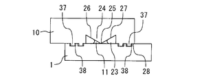
- FIG. 19 is an enlarged cross-sectional view of the joint portion between the case and the base plate of the semiconductor module according to the eighth embodiment.
- the outer peripheral portion of the upper surface of the base plate 1 and the lower surface of the case 10 come into contact with each other in a region closer to the inside of the case 10 than the groove 23.
- a concave portion 38 is provided on the outer peripheral portion of the upper surface of the base plate 1, and a convex portion 37 is provided on the lower surface of the case 10.
- the concave portion 38 has a size for accommodating the convex portion 37.
- the depth of the concave portion 38 and the height of the convex portion 37 are, for example, 1/10 or more of the thickness of the base plate 1. In order to prevent the base plate 1 from penetrating, the depth of the recess 38 is set to 4/5 or less of the thickness of the base plate 1.
- the adhesive 11 is closer to the inside of the case 10 than the predetermined position due to assembly variation, or if the amount of the adhesive 11 applied is large, the adhesive 11 spreads and reaches the contact area between the base plate 1 surface and the case 10. There is a problem that the adhesive 11 invades the inside of the case 10 due to the capillary phenomenon.
- the flow length of the adhesive 11 is increased by providing the convex portion 37 and the concave portion 38, it is possible to suppress the invasion of the adhesive 11 into the inside of the case 10. Therefore, the margin can be further increased with respect to the coating variation of the adhesive 11.
- FIG. 20 is a cross-sectional view showing a modification 1 of the eighth embodiment.
- a convex portion 37 is provided on the outer peripheral portion of the upper surface of the base plate 1
- a concave portion 38 is provided on the lower surface of the case 10. Even in this case, the same effect as that of the eighth embodiment can be obtained.
- FIG. 21 is a cross-sectional view showing a modification 2 of the eighth embodiment.
- a plurality of convex portions 37 and concave portions 38 are provided. This makes it more difficult for the adhesive 11 to penetrate the inside of the case 10.
- a convex portion 37 and a concave portion 38 are also provided in a contact region where the outer peripheral portion of the upper surface of the base plate 1 and the lower surface of the case 10 come into contact with each other on the outside of the case 10 than the groove 23. As a result, the adhesive 11 can be prevented from protruding to the outside of the case 10.
- FIG. 22 is a cross-sectional view showing a modification 3 of the eighth embodiment.
- a plurality of convex portions 37 are provided on the outer peripheral portion of the upper surface of the base plate 1, and a plurality of concave portions 38 are provided on the lower surface of the case 10. Even in this case, the same effect as that of the second modification can be obtained.
- FIG. 23 is a cross-sectional view showing the semiconductor module according to the ninth embodiment.
- FIG. 24 is an enlarged cross-sectional view of the joint portion between the case and the base plate of the semiconductor module according to the ninth embodiment.
- the upper surface of the base plate 1 is provided with a recess 39 closer to the inside than the outer peripheral portion of the upper surface to which the case 10 is joined.
- the insulating substrate 2 and the semiconductor elements 6 to 9 are provided in the recess 39.
- a convex portion 40 is provided closer to the inside of the case 10 than the groove 23 on the lower surface of the case 10.
- the convex portion 40 projects downward with respect to a portion outside the groove 23 on the lower surface of the case 10, and is inserted into the concave portion 39.
- the adhesive 11 that has been crushed and spread by joining the base plate 1 and the case 10 flows inward of the case 10, but is blocked by the convex portion 40. This makes it difficult for the adhesive 11 to penetrate the inside of the case 10. Therefore, the interface between the adhesive 11 and the sealing material 22 can be eliminated or reduced.
- Embodiment 10. 25 and 26 are enlarged cross-sectional views of the joint portion between the case and the base plate of the semiconductor module according to the tenth embodiment.
- FIG. 25 shows a state before joining the case 10 to the base plate 1
- FIG. 26 shows a state after joining.
- a protrusion 41 is provided on the lower surface of the case 10.
- the protrusion 41 is provided closer to the inside of the case 10 than the groove 23.
- the height of the protrusion 41 is, for example, 1/10 or more of the thickness of the base plate 1 and 1/2 or less of the thickness of the base plate 1.
- FIG. 27 and 28 are cross-sectional views showing a modification 1 of the tenth embodiment.
- FIG. 27 shows a state before joining the case 10 to the base plate 1
- FIG. 28 shows a state after joining.
- a high-strength material such as copper is used for the base plate 1, and the base plate 1 is provided with protrusions 41.
- the lower surface of the case 10 comes into contact with the protrusion 41 and buckles due to surface pressure to join the base plate 1 and the case 10. Even in this case, the same effect as that of the tenth embodiment can be obtained.
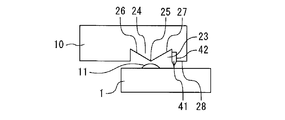
- FIG. 29 is a cross-sectional view showing a modification 2 of the tenth embodiment.
- the protrusion 41 is a metal 42 inserted into the lower surface of the case 10.
- the metal 42 has a higher strength than the base plate 1. As a result, buckling of the base plate 1 is likely to occur, and the base plate 1 and the case 10 are easily joined.
- a metal 42 may be inserted into the outer peripheral portion of the upper surface of the base plate 1 to provide a protrusion 41.
- the semiconductor elements 6 to 9 are not limited to those formed of silicon, and may be formed of a wide bandgap semiconductor having a larger bandgap than silicon.
- the wide bandgap semiconductor is, for example, silicon carbide, gallium nitride based material, or diamond.
- a power semiconductor device formed of such a wide bandgap semiconductor has high withstand voltage resistance and allowable current density, and thus can be miniaturized.
- the semiconductor module incorporating this element can also be miniaturized.
- the heat resistance of the element is high, the heat radiation fins of the heat sink can be miniaturized, and the water-cooled portion can be air-cooled, so that the semiconductor module can be further miniaturized.
Landscapes
- Engineering & Computer Science (AREA)
- Microelectronics & Electronic Packaging (AREA)
- Power Engineering (AREA)
- Physics & Mathematics (AREA)
- Condensed Matter Physics & Semiconductors (AREA)
- General Physics & Mathematics (AREA)
- Computer Hardware Design (AREA)
- Structures Or Materials For Encapsulating Or Coating Semiconductor Devices Or Solid State Devices (AREA)
- Cooling Or The Like Of Semiconductors Or Solid State Devices (AREA)
Abstract
In the present invention, an insulation substrate (2) is provided on a base plate (1). Semiconductor devices (6-9) are provided on the insulation substrate (2). A case (10) is disposed so as to surround the insulation substrate (2) and the semiconductor devices (6-9), and is joined to the base plate (1) with an adhesive (11). A sealing material (22) seals the insulation substrate (2) and the semiconductor devices (6-9) inside the case (10). A groove (23) is provided on a lower surface of the case (10) that faces an upper surface peripheral section of the base plate (1). A bottom surface of the groove (23) includes a protrusion (24) that protrudes toward the base plate (1). The protrusion (24) includes an apex (25), and slopes (26, 27) provided respectively on an inner side and an outer side of the case (10) with the apex (25) therebetween. The adhesive (11) contacts the apex (25) and is housed in the groove (23).
Description
本発明は、半導体モジュールに関する。
The present invention relates to a semiconductor module.
MOSFET(Metal Oxide Semiconductor Field Effect Transistor)、IGBT(Insulated Gate Bipolar Transistor)、ダイオードなどの電力用半導体素子を備えた半導体モジュールにおいて、ケースとベース板の接合には一般的に接着剤を用いている。ポッティング樹脂封止構造を採用したモジュールの場合、ケースの内側で接着剤と封止材との界面が生じる。接着剤と封止樹脂の材料によっては、それらの接合強度が弱いために熱サイクル応力によって界面に剥離が発生しやすい。従って、熱サイクル耐量が低下し、信頼性が損なわれるという問題があった。これを解決するためにケースに斜面を付けて接着剤がケースの内側に侵入し難くする構造が提案されている(例えば、特許文献1参照)。
In semiconductor modules equipped with power semiconductor elements such as MOSFETs (Metal Oxide Semiconductor Field Effect Transistors), IGBTs (Insulated Gate Bipolar Transistors), and diodes, adhesives are generally used to join the case and base plate. In the case of a module adopting a potting resin sealing structure, an interface between the adhesive and the sealing material is generated inside the case. Depending on the materials of the adhesive and the sealing resin, the bonding strength between them is weak, so that the interface is likely to be peeled off due to thermal cycle stress. Therefore, there is a problem that the thermodynamic cycle endurance is lowered and the reliability is impaired. In order to solve this problem, a structure has been proposed in which the case is provided with a slope to prevent the adhesive from entering the inside of the case (see, for example, Patent Document 1).
しかし、従来の構造では、接着剤塗布位置がばらついて接着剤がケースの内側に位置すると、接合後に接着剤がケースの内側に侵入しすぎる可能性がある。また、接着剤がケースの外側に位置すると、ケースとベース板が十分に接合しない可能性がある。
However, in the conventional structure, if the adhesive application position varies and the adhesive is located inside the case, the adhesive may penetrate too much inside the case after joining. Also, if the adhesive is located on the outside of the case, the case and base plate may not be sufficiently bonded.
本発明は、上述のような課題を解決するためになされたもので、その目的は熱サイクル耐量を向上させ、接着剤塗布位置のばらつきに対して裕度を大きくできる半導体モジュールを得るものである。
The present invention has been made to solve the above-mentioned problems, and an object of the present invention is to obtain a semiconductor module capable of improving the thermodynamic cycle resistance and increasing the margin with respect to the variation in the adhesive coating position. ..
本発明に係る半導体モジュールは、ベース板と、前記ベース板の上に設けられた絶縁基板と、前記絶縁基板の上に設けられた半導体素子と、前記絶縁基板及び前記半導体素子を囲むように配置され、前記ベース板に接着剤により接合されたケースと、前記ケースの内部において前記絶縁基板及び前記半導体素子を封止する封止材とを備え、前記ベース板の上面外周部に対向する前記ケースの下面に溝が設けられ、前記溝の底面は、前記ベース板に向かって突出した突出部を有し、前記突出部は、頂点と、前記頂点を挟んで前記ケースの内側寄りと外側寄りにそれぞれ設けられた勾配とを有し、前記接着剤は、前記頂点に接触し、前記溝の内部に収容されていることを特徴とする。
The semiconductor module according to the present invention is arranged so as to surround the base plate, the insulating substrate provided on the base plate, the semiconductor element provided on the insulating substrate, the insulating substrate, and the semiconductor element. The case is provided with a case bonded to the base plate with an adhesive, and a sealing material for sealing the insulating substrate and the semiconductor element inside the case, and faces the outer peripheral portion of the upper surface of the base plate. The lower surface of the groove is provided, and the bottom surface of the groove has a protruding portion protruding toward the base plate, and the protruding portion is located between the apex and the inner side and the outer side of the case with the apex in between. Each has a provided gradient, and the adhesive is in contact with the apex and is housed inside the groove.
本実施の形態では、ケースをベース板に接着剤により接合する際、接着剤が突出部の頂点に接触する。接着剤は押し潰されて突出部の勾配に沿って広がる。これにより、十分な接着面積を確保することができる。そして、接着剤の厚みによらずにケースとベース板を接合させることができる。さらに、接着剤の塗布位置のばらつきに対して裕度を大きくできる。また、押し潰された接着剤は溝の余剰スペースへ逃げるため、接着剤は溝の内部に収容され、ケースの内側まで侵入しない。このため、接着剤と封止材の界面を無くす又は低減させることができ、熱サイクル耐量を向上させることができる。
In the present embodiment, when the case is joined to the base plate with an adhesive, the adhesive comes into contact with the apex of the protruding portion. The adhesive is crushed and spreads along the slope of the protrusion. Thereby, a sufficient adhesive area can be secured. Then, the case and the base plate can be joined regardless of the thickness of the adhesive. Further, the margin can be increased with respect to the variation in the coating position of the adhesive. Further, since the crushed adhesive escapes to the excess space of the groove, the adhesive is contained inside the groove and does not penetrate to the inside of the case. Therefore, the interface between the adhesive and the sealing material can be eliminated or reduced, and the thermal cycle resistance can be improved.
実施の形態に係る半導体モジュールについて図面を参照して説明する。同じ又は対応する構成要素には同じ符号を付し、説明の繰り返しを省略する場合がある。
The semiconductor module according to the embodiment will be described with reference to the drawings. The same or corresponding components may be designated by the same reference numerals and the description may be omitted.
実施の形態1.
図1は、実施の形態1に係る半導体モジュールを示す上面図である。図2は、実施の形態1に係る半導体モジュールを示す断面図である。ベース板1の材料は銅又はアルミニウムである。ベース板1の上に絶縁基板2が設けられている。絶縁基板2の材料は、窒化ケイ素、窒化アルミニウム、酸化アルミニウム、又はZr含有アルミナなどのセラミック板である。特に、熱伝導性の点から窒化ケイ素、窒化アルミニウムが好ましく、材料強度の点から窒化ケイ素がより好ましい。絶縁基板2としてエポキシ樹脂等を用いてもよい。Embodiment 1.
FIG. 1 is a top view showing a semiconductor module according to the first embodiment. FIG. 2 is a cross-sectional view showing a semiconductor module according to the first embodiment. The material of thebase plate 1 is copper or aluminum. An insulating substrate 2 is provided on the base plate 1. The material of the insulating substrate 2 is a ceramic plate such as silicon nitride, aluminum nitride, aluminum oxide, or Zr-containing alumina. In particular, silicon nitride and aluminum nitride are preferable from the viewpoint of thermal conductivity, and silicon nitride is more preferable from the viewpoint of material strength. Epoxy resin or the like may be used as the insulating substrate 2.
図1は、実施の形態1に係る半導体モジュールを示す上面図である。図2は、実施の形態1に係る半導体モジュールを示す断面図である。ベース板1の材料は銅又はアルミニウムである。ベース板1の上に絶縁基板2が設けられている。絶縁基板2の材料は、窒化ケイ素、窒化アルミニウム、酸化アルミニウム、又はZr含有アルミナなどのセラミック板である。特に、熱伝導性の点から窒化ケイ素、窒化アルミニウムが好ましく、材料強度の点から窒化ケイ素がより好ましい。絶縁基板2としてエポキシ樹脂等を用いてもよい。
FIG. 1 is a top view showing a semiconductor module according to the first embodiment. FIG. 2 is a cross-sectional view showing a semiconductor module according to the first embodiment. The material of the
絶縁基板2の下面に金属層3が設けられている。金属層3はベース板1にはんだ等により接合されている。絶縁基板2の上に導電パターン4,5が設けられている。金属層3及び導電パターン4,5の材料はアルミニウム、アルミニウム合金、銅、又は銅合金である。特に、電気伝導性と熱伝導性に優れた銅が好ましい。
A metal layer 3 is provided on the lower surface of the insulating substrate 2. The metal layer 3 is joined to the base plate 1 by solder or the like. Conductive patterns 4 and 5 are provided on the insulating substrate 2. The material of the metal layer 3 and the conductive patterns 4 and 5 is aluminum, an aluminum alloy, copper, or a copper alloy. In particular, copper having excellent electrical conductivity and thermal conductivity is preferable.
導電パターン4の上に半導体素子6,7が設けられている。半導体素子6,7の下面電極がはんだ等により導電パターン4に接合されている。導電パターン5の上に半導体素子8,9が設けられている。半導体素子8,9の下面電極がはんだ等により導電パターン5に接合されている。半導体素子6,9は、大電流を制御するMOSFET又はIGBTなどのスイッチング素子である。半導体素子7,8は、還流ダイオードである。
Semiconductor elements 6 and 7 are provided on the conductive pattern 4. The bottom electrodes of the semiconductor elements 6 and 7 are joined to the conductive pattern 4 by solder or the like. Semiconductor elements 8 and 9 are provided on the conductive pattern 5. The bottom electrodes of the semiconductor elements 8 and 9 are joined to the conductive pattern 5 by solder or the like. The semiconductor elements 6 and 9 are switching elements such as MOSFETs or IGBTs that control a large current. The semiconductor elements 7 and 8 are freewheeling diodes.
四角い枠状のケース10が絶縁基板2及び半導体素子6~9を囲むようにベース板1の上に配置され、ベース板1の上面外周部に接着剤11により接合されている。ケース10は、半導体モジュールの使用温度領域内で熱変形を起こさず、絶縁性を維持することが求められる。このため、ケース10の材料は、PPS(Poly Phenylene Sulfide)樹脂、PBT(Poly butylene terephthalate)樹脂等の軟化点の高い樹脂である。接着剤11の材料は、例えばシリコーン樹脂、エポキシ樹脂等である。例えば、ベース板1の上面外周部に接着剤11を塗布し、ケース10をベース板1に接合した後、接着剤11を熱硬化させることで接着が行われる。
A square frame-shaped case 10 is arranged on the base plate 1 so as to surround the insulating substrate 2 and the semiconductor elements 6 to 9, and is bonded to the outer peripheral portion of the upper surface of the base plate 1 with an adhesive 11. The case 10 is required to maintain the insulating property without causing thermal deformation within the operating temperature range of the semiconductor module. Therefore, the material of the case 10 is a resin having a high softening point, such as PPS (PolyPhenylene Sulfide) resin and PBT (Polybutylene terephthalate) resin. The material of the adhesive 11 is, for example, a silicone resin, an epoxy resin, or the like. For example, the adhesive 11 is applied to the outer peripheral portion of the upper surface of the base plate 1, the case 10 is bonded to the base plate 1, and then the adhesive 11 is thermoset to perform the adhesion.
ケース10に主端子12~14と制御端子15,16が設けられている。ボンディングワイヤ17が半導体素子6,7の上面電極と主端子12を接続する。ボンディングワイヤ18が導電パターン5と主端子13を接続する。ボンディングワイヤ19が導電パターン4と半導体素子8,9の上面電極と主端子14を接続する。ボンディングワイヤ20が半導体素子6の制御電極と制御端子15を接続する。ボンディングワイヤ21が半導体素子9の制御電極と制御端子16を接続する。
The case 10 is provided with main terminals 12 to 14 and control terminals 15 and 16. The bonding wire 17 connects the top electrodes of the semiconductor elements 6 and 7 to the main terminal 12. The bonding wire 18 connects the conductive pattern 5 and the main terminal 13. The bonding wire 19 connects the conductive pattern 4, the top electrodes of the semiconductor elements 8 and 9, and the main terminal 14. The bonding wire 20 connects the control electrode of the semiconductor element 6 and the control terminal 15. The bonding wire 21 connects the control electrode of the semiconductor element 9 and the control terminal 16.
封止材22がケース10の内部において絶縁基板2、半導体素子6~9及びボンディングワイヤ17~21を封止する。ベース板1とケース10によって封止材22を密封している。封止材22は、エポキシ樹脂、フェノール樹脂、ポリイミド樹脂等であり、アルミナ、シリカなどの熱伝導性に優れた無機フィラーが添加されている。なお、接着剤11と封止材22が同系の材料の場合でも、適用用途により添加剤が異なるため、同一の線膨張係数を有するわけではない。このため、ヒートサイクルにより、線膨張係数差による熱応力が発生する場合がある。
The sealing material 22 seals the insulating substrate 2, the semiconductor elements 6 to 9, and the bonding wires 17 to 21 inside the case 10. The sealing material 22 is sealed by the base plate 1 and the case 10. The sealing material 22 is an epoxy resin, a phenol resin, a polyimide resin, or the like, and an inorganic filler having excellent thermal conductivity such as alumina or silica is added. Even when the adhesive 11 and the sealing material 22 are similar materials, they do not have the same coefficient of linear expansion because the additives differ depending on the application. Therefore, the heat cycle may generate thermal stress due to the difference in the coefficient of linear expansion.
図3は、実施の形態1に係る半導体モジュールのケースとベース板の接合部を拡大した断面図である。ベース板1の上面外周部に対向するケース10の下面に溝23が設けられている。溝23の底面は、ベース板1に向かって突出した突出部24を有する。突出部24は、頂点25と、頂点25を挟んでケース10の内側寄りと外側寄りにそれぞれ設けられた勾配26,27とを有する。接着剤11は、頂点25に接触し、溝23の内部に収容されている。溝23の幅は例えば2.6mm以上であり、接着剤11の塗布幅と位置ばらつきに応じて設定する。溝23の深さは例えば0.4mm以上であり、接着剤11の高さの想定値+0.1mm以上に設定する。突出部24の頂点25とベース板1との間隔は例えば0mm以上、0.3mm以下である。下限値0mmの場合は頂点25がベース板1に接触する。上限値0.3mmは、接着剤11の高さの想定値よりも低い。下限値に近い方が頂点25が接着剤11に接触しやすい。
FIG. 3 is an enlarged cross-sectional view of the joint portion between the case and the base plate of the semiconductor module according to the first embodiment. A groove 23 is provided on the lower surface of the case 10 facing the outer peripheral portion of the upper surface of the base plate 1. The bottom surface of the groove 23 has a protruding portion 24 protruding toward the base plate 1. The protrusion 24 has an apex 25 and gradients 26 and 27 provided on the inner side and the outer side of the case 10 with the apex 25 in between. The adhesive 11 is in contact with the apex 25 and is housed inside the groove 23. The width of the groove 23 is, for example, 2.6 mm or more, and is set according to the coating width and the positional variation of the adhesive 11. The depth of the groove 23 is, for example, 0.4 mm or more, and is set to the assumed value of the height of the adhesive 11 + 0.1 mm or more. The distance between the apex 25 of the protrusion 24 and the base plate 1 is, for example, 0 mm or more and 0.3 mm or less. When the lower limit value is 0 mm, the apex 25 comes into contact with the base plate 1. The upper limit value of 0.3 mm is lower than the assumed value of the height of the adhesive 11. The closer to the lower limit value, the easier it is for the apex 25 to come into contact with the adhesive 11.
ケース10の下面は、溝23よりもケース10の内側寄りに平面28を有する。突出部24の高さは、平面28の高さ位置を下回らず、頂点25がベース板1と接触する高さ以下である。従って、平面28はベース板1の上面外周部に面接触する。これにより、接着剤11が溝23からはみ出した場合でも、ケース10の内側へ接着剤11の侵入を防ぐことができる。また、封止材22がケース10の外側に流出するのを防ぐこともできる。
The lower surface of the case 10 has a flat surface 28 closer to the inside of the case 10 than the groove 23. The height of the protrusion 24 does not fall below the height position of the plane 28, and is equal to or less than the height at which the apex 25 contacts the base plate 1. Therefore, the flat surface 28 comes into surface contact with the outer peripheral portion of the upper surface of the base plate 1. As a result, even if the adhesive 11 protrudes from the groove 23, it is possible to prevent the adhesive 11 from invading the inside of the case 10. Further, it is possible to prevent the sealing material 22 from flowing out to the outside of the case 10.
図4は、実施の形態1に係るケースを示す下面図である。溝23はケース10の下面の全周に設けられている。このように溝23は接着剤11を塗布する領域の全周に設けることが望ましいが、信頼性が確保できる範囲内であれば一部のみに設けてもよい。
FIG. 4 is a bottom view showing the case according to the first embodiment. The groove 23 is provided on the entire circumference of the lower surface of the case 10. As described above, the groove 23 is preferably provided on the entire circumference of the region to which the adhesive 11 is applied, but may be provided only in a part thereof as long as the reliability can be ensured.
図5は、実施の形態1に係るケースの変形例1を示す下面図である。ケース10の幅が広い箇所に突出部24を有する溝23を設ける。ケース10の幅が狭い箇所には、突出部24が無く断面が矩形の溝29を設けている。このように十分なサイズの溝構造を設けることができる場所のみに溝23を設けてもよい。
FIG. 5 is a bottom view showing a modified example 1 of the case according to the first embodiment. A groove 23 having a protruding portion 24 is provided at a wide portion of the case 10. A groove 29 having no protruding portion 24 and a rectangular cross section is provided in a portion where the width of the case 10 is narrow. The groove 23 may be provided only in a place where a groove structure having a sufficient size can be provided.
図6は、実施の形態1に係るケースの変形例2を示す下面図である。ケース10は一般的に射出成型により製造する。このため、ケース10には樹脂注入経路のゲート痕と、金型から取り出す際のイジェクタピン痕が完成品に残る。そこで、ケース10のゲート痕又はイジェクタピン痕が残った領域30を避けて溝23を設けている。
FIG. 6 is a bottom view showing a modified example 2 of the case according to the first embodiment. The case 10 is generally manufactured by injection molding. Therefore, in the case 10, the gate mark of the resin injection path and the ejector pin mark when taken out from the mold remain in the finished product. Therefore, the groove 23 is provided so as to avoid the region 30 where the gate mark or the ejector pin mark of the case 10 remains.
図7から図9は、実施の形態1に係る半導体モジュールのケースをベース板に接合させる工程を示す断面図である。まず、図7に示すように、ベース板1の上面外周部に接着剤11を塗布する。次に、図8に示すようにケース10をベース板1に接合させようとすると、接着剤11が突出部24の頂点25に接触する。次に、図9に示すように更にケース10を下げると、接着剤11は押し潰されて突出部24の勾配26,27に沿って広がる。これにより、十分な接着面積を確保することができる。そして、接着剤11の厚みによらずにケース10とベース板1を接合させることができる。
7 to 9 are cross-sectional views showing a step of joining the case of the semiconductor module according to the first embodiment to the base plate. First, as shown in FIG. 7, the adhesive 11 is applied to the outer peripheral portion of the upper surface of the base plate 1. Next, when the case 10 is to be joined to the base plate 1 as shown in FIG. 8, the adhesive 11 comes into contact with the apex 25 of the protrusion 24. Next, when the case 10 is further lowered as shown in FIG. 9, the adhesive 11 is crushed and spreads along the gradients 26 and 27 of the protrusions 24. Thereby, a sufficient adhesive area can be secured. Then, the case 10 and the base plate 1 can be joined regardless of the thickness of the adhesive 11.
図10は、実施の形態1と比較例の溝と接着剤塗布位置の関係を示す断面図である。実施の形態1では突出部24の頂点25を挟んで両側に勾配26,27が設けられているのに対し、比較例では1つの勾配31しか設けられていない。このため、比較例では接着剤11が頂点25よりもケース10の内側寄りに塗布されていると、接合できなくなる。従って、接着剤11の塗布位置のばらつきに対して裕度W2が小さい。
FIG. 10 is a cross-sectional view showing the relationship between the groove of the first embodiment and the comparative example and the adhesive application position. In the first embodiment, the gradients 26 and 27 are provided on both sides of the apex 25 of the protrusion 24, whereas in the comparative example, only one gradient 31 is provided. Therefore, in the comparative example, if the adhesive 11 is applied closer to the inside of the case 10 than the apex 25, the adhesive cannot be joined. Therefore, the margin W2 is small with respect to the variation in the coating position of the adhesive 11.
これに対して、本実施の形態では、ケース10をベース板1に接着剤11により接合する際、接着剤11が突出部24の頂点25に接触し、押し潰されて突出部24の両側の勾配26,27に沿って広がる。従って、接着剤11が頂点25よりもケース10の内側寄り又は外側寄りに塗布されていても接合が可能である。このため、接着剤11の塗布位置のばらつきに対して裕度W1を大きくできる。これにより組立不良を低減させることができる。また、押し潰された接着剤11は溝23の余剰スペースへ逃げるため、接着剤11は溝23の内部に収容され、ケース10の内側まで侵入しない。このため、接着剤11と封止材22の界面を無くす又は低減させることができ、熱サイクル耐量を向上させることができる。
On the other hand, in the present embodiment, when the case 10 is joined to the base plate 1 with the adhesive 11, the adhesive 11 comes into contact with the apex 25 of the protruding portion 24 and is crushed to both sides of the protruding portion 24. It spreads along the gradients 26 and 27. Therefore, even if the adhesive 11 is applied to the inner side or the outer side of the case 10 with respect to the apex 25, the bonding is possible. Therefore, the margin W1 can be increased with respect to the variation in the coating position of the adhesive 11. As a result, assembly defects can be reduced. Further, since the crushed adhesive 11 escapes to the excess space of the groove 23, the adhesive 11 is housed inside the groove 23 and does not penetrate to the inside of the case 10. Therefore, the interface between the adhesive 11 and the sealing material 22 can be eliminated or reduced, and the thermal cycle resistance can be improved.
また、塗布位置のばらつきにより接着剤11が突出部24の頂点25に接触しない場合でも、多少のずれであれば勾配26,27とベース板1を接着剤11により接着することができる。このような場合も考慮すると、接着剤11の塗布位置のばらつきに対する裕度を更に大きくできる。
Further, even if the adhesive 11 does not come into contact with the apex 25 of the protruding portion 24 due to the variation in the coating position, the gradients 26 and 27 and the base plate 1 can be adhered by the adhesive 11 if there is a slight deviation. Considering such a case, the margin for variation in the coating position of the adhesive 11 can be further increased.
また、接着剤11は、ケース10の平面ではなく、突出部24の頂点25とその近傍の勾配26,27に接触する。従って、接着剤11が押し潰される量が少ないため、接着剤11が接合部からはみ出しにくい。
Further, the adhesive 11 comes into contact with the apex 25 of the protrusion 24 and the gradients 26 and 27 in the vicinity thereof, not on the flat surface of the case 10. Therefore, since the amount of the adhesive 11 crushed is small, the adhesive 11 does not easily protrude from the joint.
また、一般的な矩形の溝の場合、接着剤11の高さが溝の深さより低いとケース10をベース板1に接着剤11により接合できない。接着剤11の高さを大きくするために接着剤11の量を増やすと、接着剤11のはみだしのリスクが大きくなる。これに対して、本実施の形態では、溝23の底面に設けられた突出部24の頂点25が接着剤11に接触するため、接着剤11の量が少なく高さが低くても接合が可能である。従って、接着剤11の高さのばらつきに対して裕度がある。
Further, in the case of a general rectangular groove, if the height of the adhesive 11 is lower than the depth of the groove, the case 10 cannot be joined to the base plate 1 by the adhesive 11. Increasing the amount of the adhesive 11 in order to increase the height of the adhesive 11 increases the risk of the adhesive 11 sticking out. On the other hand, in the present embodiment, since the apex 25 of the protruding portion 24 provided on the bottom surface of the groove 23 comes into contact with the adhesive 11, the adhesive 11 can be joined even if the amount is small and the height is low. Is. Therefore, there is a margin for variations in the height of the adhesive 11.
なお、ボンディングワイヤ17~21の代わりに導電フレームを用いてもよい。これにより半導体モジュールの許容電流容量が増加する。また、半導体モジュールは冷却フィンにグリスを介してベース板を接続して使用することを想定しているが、冷却フィンとグリスの代わりにベース板1にピンフィンを成形してもよい。これにより組立工程を省略でき、熱抵抗が向上する。
A conductive frame may be used instead of the bonding wires 17 to 21. This increases the allowable current capacity of the semiconductor module. Further, although it is assumed that the semiconductor module is used by connecting the base plate to the cooling fins via grease, pin fins may be formed on the base plate 1 instead of the cooling fins and grease. As a result, the assembly process can be omitted and the thermal resistance is improved.
実施の形態2.
図11は、実施の形態2に係る半導体モジュールのケースとベース板の接合部を拡大した断面図である。実施の形態1ではケース10の溝23の底面に設けられた突出部24の断面が三角形であったが、本実施の形態では突出部24は所定の曲率を持つ曲面形状である。これにより、ケース10及びケース金型の割れ・欠けのリスクが低減し、部材としての耐久性が向上する。その他の構成及び効果は実施の形態1と同様である。Embodiment 2.
FIG. 11 is an enlarged cross-sectional view of the joint portion between the case and the base plate of the semiconductor module according to the second embodiment. In the first embodiment, the cross section of the protrudingportion 24 provided on the bottom surface of the groove 23 of the case 10 is triangular, but in the present embodiment, the protruding portion 24 has a curved surface shape having a predetermined curvature. As a result, the risk of cracking / chipping of the case 10 and the case mold is reduced, and the durability as a member is improved. Other configurations and effects are the same as those in the first embodiment.
図11は、実施の形態2に係る半導体モジュールのケースとベース板の接合部を拡大した断面図である。実施の形態1ではケース10の溝23の底面に設けられた突出部24の断面が三角形であったが、本実施の形態では突出部24は所定の曲率を持つ曲面形状である。これにより、ケース10及びケース金型の割れ・欠けのリスクが低減し、部材としての耐久性が向上する。その他の構成及び効果は実施の形態1と同様である。
FIG. 11 is an enlarged cross-sectional view of the joint portion between the case and the base plate of the semiconductor module according to the second embodiment. In the first embodiment, the cross section of the protruding
実施の形態3.
図12は、実施の形態3に係る半導体モジュールのケースとベース板の接合部を拡大した断面図である。ケース10の溝23の内面の全面又は一部とベース板1の接着剤11を塗布する領域の全面又は一部に表面荒らし加工32が施されている。表面荒らし加工32により表面に細かい凹凸形状が形成される。凹凸形状の高低差は例えば0.01mm以上である。これにより、接着剤11の流動長が長くなると共に、接着剤11の流動が抑制される。このため、接着剤11がケース10の内側に更に侵入しづらくなる。従って、接着剤11と封止材22の界面を無くす又は更に低減させることができる。その他の構成及び効果は実施の形態1と同様である。Embodiment 3.
FIG. 12 is an enlarged cross-sectional view of the joint portion between the case and the base plate of the semiconductor module according to the third embodiment. Thesurface roughening process 32 is applied to the entire surface or part of the inner surface of the groove 23 of the case 10 and the entire surface or part of the area to which the adhesive 11 of the base plate 1 is applied. A fine uneven shape is formed on the surface by the surface roughening process 32. The height difference of the uneven shape is, for example, 0.01 mm or more. As a result, the flow length of the adhesive 11 becomes long, and the flow of the adhesive 11 is suppressed. Therefore, it becomes more difficult for the adhesive 11 to penetrate the inside of the case 10. Therefore, the interface between the adhesive 11 and the sealing material 22 can be eliminated or further reduced. Other configurations and effects are the same as those in the first embodiment.
図12は、実施の形態3に係る半導体モジュールのケースとベース板の接合部を拡大した断面図である。ケース10の溝23の内面の全面又は一部とベース板1の接着剤11を塗布する領域の全面又は一部に表面荒らし加工32が施されている。表面荒らし加工32により表面に細かい凹凸形状が形成される。凹凸形状の高低差は例えば0.01mm以上である。これにより、接着剤11の流動長が長くなると共に、接着剤11の流動が抑制される。このため、接着剤11がケース10の内側に更に侵入しづらくなる。従って、接着剤11と封止材22の界面を無くす又は更に低減させることができる。その他の構成及び効果は実施の形態1と同様である。
FIG. 12 is an enlarged cross-sectional view of the joint portion between the case and the base plate of the semiconductor module according to the third embodiment. The
実施の形態4.
図13は、実施の形態4に係る半導体モジュールのケースとベース板の接合部を拡大した断面図である。ベース板1の接着剤11を塗布する領域の全面又は一部に格子状のシート33が貼り付けられている。これにより実施の形態3と同様の効果を得ることができる。その他の構成及び効果は実施の形態1と同様である。Embodiment 4.
FIG. 13 is an enlarged cross-sectional view of the joint portion between the case and the base plate of the semiconductor module according to the fourth embodiment. A grid-like sheet 33 is attached to the entire surface or a part of the area of the base plate 1 to which the adhesive 11 is applied. As a result, the same effect as that of the third embodiment can be obtained. Other configurations and effects are the same as those in the first embodiment.
図13は、実施の形態4に係る半導体モジュールのケースとベース板の接合部を拡大した断面図である。ベース板1の接着剤11を塗布する領域の全面又は一部に格子状のシート33が貼り付けられている。これにより実施の形態3と同様の効果を得ることができる。その他の構成及び効果は実施の形態1と同様である。
FIG. 13 is an enlarged cross-sectional view of the joint portion between the case and the base plate of the semiconductor module according to the fourth embodiment. A grid-
実施の形態5.
図14は、実施の形態5に係る半導体モジュールのケースとベース板の接合部を拡大した断面図である。溝23に対向するベース板1の上面外周部であって接着剤11を塗布する領域よりもケース10の内側の領域にボンディングワイヤ34が設けられている。これにより実施の形態3と同様の効果を得ることができる。その他の構成及び効果は実施の形態1と同様である。なお、接着剤11を塗布する領域よりもケース10の外側の領域にもボンディングワイヤ34を設けてもよい。これにより接着剤11がケース10の外側にはみ出すのを防ぐことができる。Embodiment 5.
FIG. 14 is an enlarged cross-sectional view of the joint portion between the case and the base plate of the semiconductor module according to the fifth embodiment. Thebonding wire 34 is provided in the outer peripheral portion of the upper surface of the base plate 1 facing the groove 23 and in the region inside the case 10 with respect to the region where the adhesive 11 is applied. As a result, the same effect as that of the third embodiment can be obtained. Other configurations and effects are the same as those in the first embodiment. The bonding wire 34 may be provided in a region outside the case 10 as well as a region to which the adhesive 11 is applied. As a result, the adhesive 11 can be prevented from protruding to the outside of the case 10.
図14は、実施の形態5に係る半導体モジュールのケースとベース板の接合部を拡大した断面図である。溝23に対向するベース板1の上面外周部であって接着剤11を塗布する領域よりもケース10の内側の領域にボンディングワイヤ34が設けられている。これにより実施の形態3と同様の効果を得ることができる。その他の構成及び効果は実施の形態1と同様である。なお、接着剤11を塗布する領域よりもケース10の外側の領域にもボンディングワイヤ34を設けてもよい。これにより接着剤11がケース10の外側にはみ出すのを防ぐことができる。
FIG. 14 is an enlarged cross-sectional view of the joint portion between the case and the base plate of the semiconductor module according to the fifth embodiment. The
実施の形態6.
図15は、実施の形態6に係る半導体モジュールのケースとベース板の接合部を拡大した断面図である。ケース10の溝23に対向してベース板1に凹部35が設けられている。凹部35の底面に接着剤11が塗布されている。凹部35の幅は、接着剤11を塗布する領域の幅より広く、溝23の幅より狭い。突出部24の高さは、頂点25が凹部35内の接着剤11と接触する高さに設定されている。凹部35の深さは例えば0.1mm以上であるが、ベース板1の貫通を防ぐためにベース板1の厚みの4/5以下にする。Embodiment 6.
FIG. 15 is an enlarged cross-sectional view of the joint portion between the case and the base plate of the semiconductor module according to the sixth embodiment. Arecess 35 is provided in the base plate 1 so as to face the groove 23 of the case 10. The adhesive 11 is applied to the bottom surface of the recess 35. The width of the recess 35 is wider than the width of the area to which the adhesive 11 is applied and narrower than the width of the groove 23. The height of the protrusion 24 is set to a height at which the apex 25 comes into contact with the adhesive 11 in the recess 35. The depth of the recess 35 is, for example, 0.1 mm or more, but it is set to 4/5 or less of the thickness of the base plate 1 in order to prevent the base plate 1 from penetrating.
図15は、実施の形態6に係る半導体モジュールのケースとベース板の接合部を拡大した断面図である。ケース10の溝23に対向してベース板1に凹部35が設けられている。凹部35の底面に接着剤11が塗布されている。凹部35の幅は、接着剤11を塗布する領域の幅より広く、溝23の幅より狭い。突出部24の高さは、頂点25が凹部35内の接着剤11と接触する高さに設定されている。凹部35の深さは例えば0.1mm以上であるが、ベース板1の貫通を防ぐためにベース板1の厚みの4/5以下にする。
FIG. 15 is an enlarged cross-sectional view of the joint portion between the case and the base plate of the semiconductor module according to the sixth embodiment. A
凹部35を設けたことで接着剤11の収容スペースが広くなる。このため、接着剤11がケース10の内側に更に侵入しづらくなる。従って、接着剤11と封止材22の界面を無くす又は更に低減させることができる。その他の構成及び効果は実施の形態1と同様である。
By providing the recess 35, the storage space for the adhesive 11 is widened. Therefore, it becomes more difficult for the adhesive 11 to penetrate the inside of the case 10. Therefore, the interface between the adhesive 11 and the sealing material 22 can be eliminated or further reduced. Other configurations and effects are the same as those in the first embodiment.
実施の形態7.
図16は、実施の形態7に係る半導体モジュールのケースとベース板の接合部を拡大した断面図である。ケース10の下面と対向する領域においてベース板1の上面外周部に凹部36が設けられている。凹部36は、接着剤11を塗布する領域よりもケース10の内側の領域に設けられている。凹部36の深さは例えばベース板1の厚みの1/10以上であるが、ベース板1の貫通を防ぐためにベース板1の厚みの4/5以下にする。Embodiment 7.
FIG. 16 is an enlarged cross-sectional view of the joint portion between the case and the base plate of the semiconductor module according to the seventh embodiment. Arecess 36 is provided on the outer peripheral portion of the upper surface of the base plate 1 in a region facing the lower surface of the case 10. The recess 36 is provided in a region inside the case 10 with respect to the region where the adhesive 11 is applied. The depth of the recess 36 is, for example, 1/10 or more of the thickness of the base plate 1, but is set to 4/5 or less of the thickness of the base plate 1 in order to prevent penetration of the base plate 1.
図16は、実施の形態7に係る半導体モジュールのケースとベース板の接合部を拡大した断面図である。ケース10の下面と対向する領域においてベース板1の上面外周部に凹部36が設けられている。凹部36は、接着剤11を塗布する領域よりもケース10の内側の領域に設けられている。凹部36の深さは例えばベース板1の厚みの1/10以上であるが、ベース板1の貫通を防ぐためにベース板1の厚みの4/5以下にする。
FIG. 16 is an enlarged cross-sectional view of the joint portion between the case and the base plate of the semiconductor module according to the seventh embodiment. A
ベース板1とケース10により押し潰された接着剤11が凹部36に収容される。このため、接着剤11がケース10の内側に更に侵入しづらくなる。従って、接着剤11と封止材22の界面を無くす又は更に低減させることができる。その他の構成及び効果は実施の形態1と同様である。
The adhesive 11 crushed by the base plate 1 and the case 10 is housed in the recess 36. Therefore, it becomes more difficult for the adhesive 11 to penetrate the inside of the case 10. Therefore, the interface between the adhesive 11 and the sealing material 22 can be eliminated or further reduced. Other configurations and effects are the same as those in the first embodiment.
図17は、実施の形態7の変形例1を示す断面図である。変形例1のように連なった複数の凹部36を設けてもよい。これにより、接着剤11が直近の1つ目の凹部36を超えて広がった場合であっても、2つ目以降の凹部36に収容される。このため、接着剤11がケース10の内側に更に侵入しづらくなる。
FIG. 17 is a cross-sectional view showing a modification 1 of the seventh embodiment. A plurality of continuous recesses 36 may be provided as in the first modification. As a result, even when the adhesive 11 spreads beyond the nearest first recess 36, it is accommodated in the second and subsequent recesses 36. Therefore, it becomes more difficult for the adhesive 11 to penetrate the inside of the case 10.
図18は、実施の形態7の変形例2を示す断面図である。変形例2のように接着剤11を塗布する領域よりもケース10の内側寄りと外側寄りの領域に複数の凹部36を設けてもよい。これにより接着剤11がケース10の外側にはみ出すのを防ぐことができる。
FIG. 18 is a cross-sectional view showing a modification 2 of the seventh embodiment. A plurality of recesses 36 may be provided in the areas closer to the inside and the outside of the case 10 than the area to which the adhesive 11 is applied as in the second modification. As a result, the adhesive 11 can be prevented from protruding to the outside of the case 10.
実施の形態8.
図19は、実施の形態8に係る半導体モジュールのケースとベース板の接合部を拡大した断面図である。溝23よりもケース10の内側寄りの領域においてベース板1の上面外周部とケース10の下面が接触する。この接触領域において、ベース板1の上面外周部に凹部38が設けられ、ケース10の下面に凸部37が設けられている。凹部38は凸部37を収容する大きさを持つ。ケース10がベース板1に接着剤11により接合された際に凸部37と凹部38が嵌合する。凹部38の深さ及び凸部37の高さは例えばベース板1の厚みの1/10以上である。ベース板1の貫通を防ぐために、凹部38の深さはベース板1の厚みの4/5以下にする。Embodiment 8.
FIG. 19 is an enlarged cross-sectional view of the joint portion between the case and the base plate of the semiconductor module according to the eighth embodiment. The outer peripheral portion of the upper surface of thebase plate 1 and the lower surface of the case 10 come into contact with each other in a region closer to the inside of the case 10 than the groove 23. In this contact region, a concave portion 38 is provided on the outer peripheral portion of the upper surface of the base plate 1, and a convex portion 37 is provided on the lower surface of the case 10. The concave portion 38 has a size for accommodating the convex portion 37. When the case 10 is joined to the base plate 1 by the adhesive 11, the convex portion 37 and the concave portion 38 are fitted. The depth of the concave portion 38 and the height of the convex portion 37 are, for example, 1/10 or more of the thickness of the base plate 1. In order to prevent the base plate 1 from penetrating, the depth of the recess 38 is set to 4/5 or less of the thickness of the base plate 1.
図19は、実施の形態8に係る半導体モジュールのケースとベース板の接合部を拡大した断面図である。溝23よりもケース10の内側寄りの領域においてベース板1の上面外周部とケース10の下面が接触する。この接触領域において、ベース板1の上面外周部に凹部38が設けられ、ケース10の下面に凸部37が設けられている。凹部38は凸部37を収容する大きさを持つ。ケース10がベース板1に接着剤11により接合された際に凸部37と凹部38が嵌合する。凹部38の深さ及び凸部37の高さは例えばベース板1の厚みの1/10以上である。ベース板1の貫通を防ぐために、凹部38の深さはベース板1の厚みの4/5以下にする。
FIG. 19 is an enlarged cross-sectional view of the joint portion between the case and the base plate of the semiconductor module according to the eighth embodiment. The outer peripheral portion of the upper surface of the
組立ばらつきにより接着剤11が所定位置よりもケース10の内側寄りになるか又は接着剤11の塗布量が多いと、接着剤11が広がってベース板1面とケース10の接触領域に到達し、接着剤11が毛細管現象によってケース10の内側へ侵入するという問題がある。これに対して、本実施の形態では、凸部37と凹部38を設けることで接着剤11の流動長が長くなるため、ケース10の内側への接着剤11の侵入を抑制することができる。従って、接着剤11の塗布ばらつきに対して更に裕度を大きくできる。
If the adhesive 11 is closer to the inside of the case 10 than the predetermined position due to assembly variation, or if the amount of the adhesive 11 applied is large, the adhesive 11 spreads and reaches the contact area between the base plate 1 surface and the case 10. There is a problem that the adhesive 11 invades the inside of the case 10 due to the capillary phenomenon. On the other hand, in the present embodiment, since the flow length of the adhesive 11 is increased by providing the convex portion 37 and the concave portion 38, it is possible to suppress the invasion of the adhesive 11 into the inside of the case 10. Therefore, the margin can be further increased with respect to the coating variation of the adhesive 11.
図20は、実施の形態8の変形例1を示す断面図である。変形例1では、図19とは逆に、ベース板1の上面外周部に凸部37が設けられ、ケース10の下面に凹部38が設けられている。この場合でも実施の形態8と同様の効果を得ることができる。
FIG. 20 is a cross-sectional view showing a modification 1 of the eighth embodiment. In the first modification, contrary to FIG. 19, a convex portion 37 is provided on the outer peripheral portion of the upper surface of the base plate 1, and a concave portion 38 is provided on the lower surface of the case 10. Even in this case, the same effect as that of the eighth embodiment can be obtained.
図21は、実施の形態8の変形例2を示す断面図である。変形例2では、凸部37と凹部38が複数設けられている。これにより接着剤11がケース10の内側に更に侵入しづらくなる。また、溝23よりもケース10の外側においてベース板1の上面外周部とケース10の下面が接触する接触領域にも凸部37と凹部38が設けられている。これにより接着剤11がケース10の外側にはみ出すのを防ぐことができる。
FIG. 21 is a cross-sectional view showing a modification 2 of the eighth embodiment. In the second modification, a plurality of convex portions 37 and concave portions 38 are provided. This makes it more difficult for the adhesive 11 to penetrate the inside of the case 10. Further, a convex portion 37 and a concave portion 38 are also provided in a contact region where the outer peripheral portion of the upper surface of the base plate 1 and the lower surface of the case 10 come into contact with each other on the outside of the case 10 than the groove 23. As a result, the adhesive 11 can be prevented from protruding to the outside of the case 10.
図22は、実施の形態8の変形例3を示す断面図である。変形例3では、変形例2とは逆に、ベース板1の上面外周部に複数の凸部37が設けられ、ケース10の下面に複数の凹部38が設けられている。この場合でも変形例2と同様の効果を得ることができる。
FIG. 22 is a cross-sectional view showing a modification 3 of the eighth embodiment. In the third modification, contrary to the second modification, a plurality of convex portions 37 are provided on the outer peripheral portion of the upper surface of the base plate 1, and a plurality of concave portions 38 are provided on the lower surface of the case 10. Even in this case, the same effect as that of the second modification can be obtained.
実施の形態9.
図23は、実施の形態9に係る半導体モジュールを示す断面図である。図24は、実施の形態9に係る半導体モジュールのケースとベース板の接合部を拡大した断面図である。ベース板1の上面には、ケース10が接合される上面外周部よりも内側寄りに凹部39が設けられている。凹部39に絶縁基板2及び半導体素子6~9が設けられている。これにより、パッケージサイズを小さくでき、熱抵抗が向上し、モジュール裏面の反りを調整できる。Embodiment 9.
FIG. 23 is a cross-sectional view showing the semiconductor module according to the ninth embodiment. FIG. 24 is an enlarged cross-sectional view of the joint portion between the case and the base plate of the semiconductor module according to the ninth embodiment. The upper surface of thebase plate 1 is provided with a recess 39 closer to the inside than the outer peripheral portion of the upper surface to which the case 10 is joined. The insulating substrate 2 and the semiconductor elements 6 to 9 are provided in the recess 39. As a result, the package size can be reduced, the thermal resistance can be improved, and the warp of the back surface of the module can be adjusted.
図23は、実施の形態9に係る半導体モジュールを示す断面図である。図24は、実施の形態9に係る半導体モジュールのケースとベース板の接合部を拡大した断面図である。ベース板1の上面には、ケース10が接合される上面外周部よりも内側寄りに凹部39が設けられている。凹部39に絶縁基板2及び半導体素子6~9が設けられている。これにより、パッケージサイズを小さくでき、熱抵抗が向上し、モジュール裏面の反りを調整できる。
FIG. 23 is a cross-sectional view showing the semiconductor module according to the ninth embodiment. FIG. 24 is an enlarged cross-sectional view of the joint portion between the case and the base plate of the semiconductor module according to the ninth embodiment. The upper surface of the
ケース10の下面の溝23よりもケース10の内側寄りに凸部40が設けられている。凸部40は、ケース10の下面の溝23よりも外側の部分に対して下方に突出し、凹部39に挿入されている。ベース板1とケース10の接合により潰れて広がった接着剤11がケース10の内側へ流動するが、凸部40によって塞き止められる。これにより、接着剤11がケース10の内側に侵入しづらくなる。従って、接着剤11と封止材22の界面を無くす又は低減させることができる。
A convex portion 40 is provided closer to the inside of the case 10 than the groove 23 on the lower surface of the case 10. The convex portion 40 projects downward with respect to a portion outside the groove 23 on the lower surface of the case 10, and is inserted into the concave portion 39. The adhesive 11 that has been crushed and spread by joining the base plate 1 and the case 10 flows inward of the case 10, but is blocked by the convex portion 40. This makes it difficult for the adhesive 11 to penetrate the inside of the case 10. Therefore, the interface between the adhesive 11 and the sealing material 22 can be eliminated or reduced.
実施の形態10.
図25及び図26は、実施の形態10に係る半導体モジュールのケースとベース板の接合部を拡大した断面図である。図25はケース10をベース板1に接合する前の状態、図26は接合後の状態を示す。ケース10の下面に突起41が設けられている。突起41は、溝23よりもケース10の内側寄りに設けられている。突起41の高さは例えばベース板1の厚みの1/10以上、ベース板1の厚みの1/2以下である。ベース板1の材料として、突起41よりも強度の低いアルミ材などを使用する。Embodiment 10.
25 and 26 are enlarged cross-sectional views of the joint portion between the case and the base plate of the semiconductor module according to the tenth embodiment. FIG. 25 shows a state before joining thecase 10 to the base plate 1, and FIG. 26 shows a state after joining. A protrusion 41 is provided on the lower surface of the case 10. The protrusion 41 is provided closer to the inside of the case 10 than the groove 23. The height of the protrusion 41 is, for example, 1/10 or more of the thickness of the base plate 1 and 1/2 or less of the thickness of the base plate 1. As the material of the base plate 1, an aluminum material having a strength lower than that of the protrusion 41 is used.
図25及び図26は、実施の形態10に係る半導体モジュールのケースとベース板の接合部を拡大した断面図である。図25はケース10をベース板1に接合する前の状態、図26は接合後の状態を示す。ケース10の下面に突起41が設けられている。突起41は、溝23よりもケース10の内側寄りに設けられている。突起41の高さは例えばベース板1の厚みの1/10以上、ベース板1の厚みの1/2以下である。ベース板1の材料として、突起41よりも強度の低いアルミ材などを使用する。
25 and 26 are enlarged cross-sectional views of the joint portion between the case and the base plate of the semiconductor module according to the tenth embodiment. FIG. 25 shows a state before joining the
ケース10をベース板1に接着する際にベース板1の上面外周部が突起41に接触して面圧で座屈してベース板1の上面外周部とケース10の下面が接合される。これにより隙間の無い又は小さい接合が可能となるため、接着剤11がケース10の内側に更に侵入しづらくなる。従って、接着剤11と封止材22の界面を無くす又は低減させることができる。
When the case 10 is adhered to the base plate 1, the outer peripheral portion of the upper surface of the base plate 1 comes into contact with the protrusion 41 and buckles due to surface pressure to join the outer peripheral portion of the upper surface of the base plate 1 and the lower surface of the case 10. As a result, it becomes possible to join the adhesive without gaps or with a small gap, so that the adhesive 11 is more difficult to penetrate inside the case 10. Therefore, the interface between the adhesive 11 and the sealing material 22 can be eliminated or reduced.
図27及び図28は、実施の形態10の変形例1を示す断面図である。図27はケース10をベース板1に接合する前の状態、図28は接合後の状態を示す。ベース板1に銅などの強度の高い材料を使用し、ベース板1に突起41を設けている。この場合、ケース10の下面が突起41に接触して面圧で座屈してベース板1とケース10が接合される。この場合でも実施の形態10と同様の効果を得ることができる。
27 and 28 are cross-sectional views showing a modification 1 of the tenth embodiment. FIG. 27 shows a state before joining the case 10 to the base plate 1, and FIG. 28 shows a state after joining. A high-strength material such as copper is used for the base plate 1, and the base plate 1 is provided with protrusions 41. In this case, the lower surface of the case 10 comes into contact with the protrusion 41 and buckles due to surface pressure to join the base plate 1 and the case 10. Even in this case, the same effect as that of the tenth embodiment can be obtained.
図29は、実施の形態10の変形例2を示す断面図である。突起41は、ケース10の下面にインサートされた金属42である。金属42はベース板1よりも高い強度を持つ。これにより、ベース板1の座屈が発生しやすくなり、ベース板1とケース10を接合しやすくなる。なお、ベース板1の上面外周部に金属42をインサートして突起41を設けてもよい。
FIG. 29 is a cross-sectional view showing a modification 2 of the tenth embodiment. The protrusion 41 is a metal 42 inserted into the lower surface of the case 10. The metal 42 has a higher strength than the base plate 1. As a result, buckling of the base plate 1 is likely to occur, and the base plate 1 and the case 10 are easily joined. A metal 42 may be inserted into the outer peripheral portion of the upper surface of the base plate 1 to provide a protrusion 41.
なお、半導体素子6~9は、珪素によって形成されたものに限らず、珪素に比べてバンドギャップが大きいワイドバンドギャップ半導体によって形成されたものでもよい。ワイドバンドギャップ半導体は、例えば、炭化珪素、窒化ガリウム系材料、又はダイヤモンドである。このようなワイドバンドギャップ半導体によって形成されたパワー半導体素子は、耐電圧性と許容電流密度が高いため、小型化できる。この小型化された素子を用いることで、この素子を組み込んだ半導体モジュールも小型化できる。また、素子の耐熱性が高いため、ヒートシンクの放熱フィンを小型化でき、水冷部を空冷化できるので、半導体モジュールを更に小型化できる。
Note that the semiconductor elements 6 to 9 are not limited to those formed of silicon, and may be formed of a wide bandgap semiconductor having a larger bandgap than silicon. The wide bandgap semiconductor is, for example, silicon carbide, gallium nitride based material, or diamond. A power semiconductor device formed of such a wide bandgap semiconductor has high withstand voltage resistance and allowable current density, and thus can be miniaturized. By using this miniaturized element, the semiconductor module incorporating this element can also be miniaturized. Further, since the heat resistance of the element is high, the heat radiation fins of the heat sink can be miniaturized, and the water-cooled portion can be air-cooled, so that the semiconductor module can be further miniaturized.
1 ベース板、2 絶縁基板、6~9 半導体素子、10 ケース、11 接着剤、22 封止材、23 溝、24 突出部、25 頂点、26,27 勾配、32 表面荒らし加工、33 格子状のシート、34 ボンディングワイヤ、35,36,38,39 凹部、37,40 凸部、41 突起、42 金属
1 base plate, 2 insulating substrate, 6-9 semiconductor elements, 10 cases, 11 adhesives, 22 encapsulants, 23 grooves, 24 protrusions, 25 vertices, 26, 27 gradients, 32 surface roughening, 33 grid-like Sheet, 34 bonding wire, 35, 36, 38, 39 concave, 37, 40 convex, 41 protrusion, 42 metal
Claims (19)
- ベース板と、
前記ベース板の上に設けられた絶縁基板と、
前記絶縁基板の上に設けられた半導体素子と、
前記絶縁基板及び前記半導体素子を囲むように配置され、前記ベース板に接着剤により接合されたケースと、
前記ケースの内部において前記絶縁基板及び前記半導体素子を封止する封止材とを備え、
前記ベース板の上面外周部に対向する前記ケースの下面に溝が設けられ、
前記溝の底面は、前記ベース板に向かって突出した突出部を有し、
前記突出部は、頂点と、前記頂点を挟んで前記ケースの内側寄りと外側寄りにそれぞれ設けられた勾配とを有し、
前記接着剤は、前記頂点に接触し、前記溝の内部に収容されていることを特徴とする半導体モジュール。 With the base plate
An insulating substrate provided on the base plate and
A semiconductor element provided on the insulating substrate and
A case arranged so as to surround the insulating substrate and the semiconductor element and bonded to the base plate with an adhesive, and a case.
A sealing material for sealing the insulating substrate and the semiconductor element is provided inside the case.
A groove is provided on the lower surface of the case facing the outer peripheral portion of the upper surface of the base plate.
The bottom surface of the groove has a protrusion protruding toward the base plate.
The protrusion has an apex and a gradient provided on the inner side and the outer side of the case with the apex in between.
A semiconductor module characterized in that the adhesive is in contact with the apex and is housed inside the groove. - 前記突出部の高さは、前記頂点が前記ベース板と接触する高さ以下であることを特徴とする請求項1に記載の半導体モジュール。 The semiconductor module according to claim 1, wherein the height of the protruding portion is equal to or less than a height at which the apex comes into contact with the base plate.
- 前記突出部は曲面形状であることを特徴とする請求項1又は2に記載の半導体モジュール。 The semiconductor module according to claim 1 or 2, wherein the protruding portion has a curved surface shape.
- 前記ケースの前記溝の内面と前記ベース板の前記接着剤を塗布する領域に表面荒らし加工が施されていることを特徴とする請求項1~3の何れか1項に記載の半導体モジュール。 The semiconductor module according to any one of claims 1 to 3, wherein the inner surface of the groove of the case and the region of the base plate to which the adhesive is applied are surface-roughened.
- 前記ベース板の前記接着剤を塗布する領域に格子状のシートが貼り付けられていることを特徴とする請求項1~3の何れか1項に記載の半導体モジュール。 The semiconductor module according to any one of claims 1 to 3, wherein a grid-like sheet is attached to a region of the base plate to which the adhesive is applied.
- 前記溝に対向する前記ベース板の上面外周部にボンディングワイヤが設けられていることを特徴とする請求項1~3の何れか1項に記載の半導体モジュール。 The semiconductor module according to any one of claims 1 to 3, wherein a bonding wire is provided on the outer peripheral portion of the upper surface of the base plate facing the groove.
- 前記ボンディングワイヤは、前記接着剤を塗布する領域よりも前記ケースの内側寄りに設けられていることを特徴とする請求項6に記載の半導体モジュール。 The semiconductor module according to claim 6, wherein the bonding wire is provided closer to the inside of the case than the region to which the adhesive is applied.
- 前記ベース板に凹部が設けられ、
前記凹部に前記接着剤が塗布されていることを特徴とする請求項1~3の何れか1項に記載の半導体モジュール。 A recess is provided in the base plate.
The semiconductor module according to any one of claims 1 to 3, wherein the adhesive is applied to the recess. - 前記ケースの下面が対向する前記ベース板の上面外周部に凹部が設けられていることを特徴とする請求項1~3の何れか1項に記載の半導体モジュール。 The semiconductor module according to any one of claims 1 to 3, wherein a recess is provided in the outer peripheral portion of the upper surface of the base plate facing the lower surface of the case.
- 前記凹部は、前記接着剤を塗布する領域よりも前記ケースの内側寄りに設けられていることを特徴とする請求項9に記載の半導体モジュール。 The semiconductor module according to claim 9, wherein the recess is provided closer to the inside of the case than the region to which the adhesive is applied.
- 前記凹部は複数設けられていることを特徴とする請求項9又は10に記載の半導体モジュール。 The semiconductor module according to claim 9 or 10, wherein a plurality of the recesses are provided.
- 前記ベース板の上面外周部と前記ケースの下面の一方に凸部が設けられ、他方に凹部が設けられ、前記凸部と前記凹部が嵌合することを特徴とする請求項1~3の何れか1項に記載の半導体モジュール。 Any of claims 1 to 3, wherein a convex portion is provided on one of the outer peripheral portion of the upper surface of the base plate and the lower surface of the case, and a concave portion is provided on the other, and the convex portion and the concave portion are fitted. The semiconductor module according to item 1.
- 前記凸部と前記凹部は、前記溝よりも前記ケースの内側寄りに設けられていることを特徴とする請求項12に記載の半導体モジュール。 The semiconductor module according to claim 12, wherein the convex portion and the concave portion are provided closer to the inside of the case than the groove.
- 前記凸部と前記凹部はそれぞれ複数設けられていることを特徴とする請求項12又は13に記載の半導体モジュール。 The semiconductor module according to claim 12 or 13, wherein a plurality of the convex portion and the concave portion are provided.
- 前記ベース板の上面には、前記ケースが接合される前記上面外周部よりも内側寄りに凹部が設けられ、
前記凹部に前記絶縁基板及び前記半導体素子が設けられ、
前記ケースの下面の前記溝よりも前記ケースの内側寄りに凸部が設けられ、
前記凸部は前記凹部に挿入されていることを特徴とする請求項1~3の何れか1項に記載の半導体モジュール。 The upper surface of the base plate is provided with a recess on the inner side of the outer peripheral portion of the upper surface to which the case is joined.
The insulating substrate and the semiconductor element are provided in the recess, and the insulating substrate and the semiconductor element are provided.
A convex portion is provided on the inner surface of the case with respect to the groove on the lower surface of the case.
The semiconductor module according to any one of claims 1 to 3, wherein the convex portion is inserted into the concave portion. - 前記ベース板の上面外周部と前記ケースの下面の一方に突起が設けられ、他方が前記突起に接触して面圧で座屈して前記ベース板と前記ケースが接合されていることを特徴とする請求項1~3の何れか1項に記載の半導体モジュール。 A protrusion is provided on one of the outer peripheral portion of the upper surface of the base plate and the lower surface of the case, and the other is in contact with the protrusion and buckled by surface pressure to join the base plate and the case. The semiconductor module according to any one of claims 1 to 3.
- 前記突起は、前記溝よりも前記ケースの内側寄りに設けられていることを特徴とする請求項16に記載の半導体モジュール。 The semiconductor module according to claim 16, wherein the protrusion is provided closer to the inside of the case than the groove.
- 前記突起は、前記ベース板の上面外周部と前記ケースの下面の一方にインサートされた金属であり、他方よりも高い強度を持つことを特徴とする請求項16又は17に記載の半導体モジュール。 The semiconductor module according to claim 16 or 17, wherein the protrusion is a metal inserted into one of the outer peripheral portion of the upper surface of the base plate and the lower surface of the case, and has higher strength than the other.
- 前記半導体素子はワイドバンドギャップ半導体によって形成されていることを特徴とする請求項1~18の何れか1項に記載の半導体モジュール。 The semiconductor module according to any one of claims 1 to 18, wherein the semiconductor element is formed of a wide bandgap semiconductor.
Priority Applications (5)
| Application Number | Priority Date | Filing Date | Title |
|---|---|---|---|
| PCT/JP2019/046445 WO2021106114A1 (en) | 2019-11-27 | 2019-11-27 | Semiconductor module |
| CN201980102435.8A CN114730745A (en) | 2019-11-27 | 2019-11-27 | Semiconductor module |
| JP2021560830A JP7173375B2 (en) | 2019-11-27 | 2019-11-27 | semiconductor module |
| US17/627,171 US20220278004A1 (en) | 2019-11-27 | 2019-11-27 | Semiconductor module |
| DE112019007915.8T DE112019007915T5 (en) | 2019-11-27 | 2019-11-27 | semiconductor module |
Applications Claiming Priority (1)
| Application Number | Priority Date | Filing Date | Title |
|---|---|---|---|
| PCT/JP2019/046445 WO2021106114A1 (en) | 2019-11-27 | 2019-11-27 | Semiconductor module |
Publications (1)
| Publication Number | Publication Date |
|---|---|
| WO2021106114A1 true WO2021106114A1 (en) | 2021-06-03 |
Family
ID=76128686
Family Applications (1)
| Application Number | Title | Priority Date | Filing Date |
|---|---|---|---|
| PCT/JP2019/046445 WO2021106114A1 (en) | 2019-11-27 | 2019-11-27 | Semiconductor module |
Country Status (5)
| Country | Link |
|---|---|
| US (1) | US20220278004A1 (en) |
| JP (1) | JP7173375B2 (en) |
| CN (1) | CN114730745A (en) |
| DE (1) | DE112019007915T5 (en) |
| WO (1) | WO2021106114A1 (en) |
Cited By (1)
| Publication number | Priority date | Publication date | Assignee | Title |
|---|---|---|---|---|
| JP2021150575A (en) * | 2020-03-23 | 2021-09-27 | 株式会社東芝 | Semiconductor device |
Citations (13)
| Publication number | Priority date | Publication date | Assignee | Title |
|---|---|---|---|---|
| JPS553617A (en) * | 1978-06-21 | 1980-01-11 | Hitachi Ltd | Metallic base for hybrid integrated circuit |
| JPS61139048A (en) * | 1984-12-11 | 1986-06-26 | Toshiba Corp | Semiconductor device |
| JPS63100842U (en) * | 1986-12-19 | 1988-06-30 | ||
| JPS6417455A (en) * | 1987-07-10 | 1989-01-20 | Mitsubishi Electric Corp | Semiconductor device |
| JPH06268102A (en) * | 1993-01-13 | 1994-09-22 | Fuji Electric Co Ltd | Resin sealed semiconductor device |
| JP2000323593A (en) * | 1999-05-06 | 2000-11-24 | Yazaki Corp | Semiconductor device |
| JP2004103846A (en) * | 2002-09-10 | 2004-04-02 | Mitsubishi Electric Corp | Semiconductor device for electric power |
| JP2005322784A (en) * | 2004-05-10 | 2005-11-17 | Mitsubishi Electric Corp | Semiconductor device for electric power |
| JP2012015349A (en) * | 2010-07-01 | 2012-01-19 | Fuji Electric Co Ltd | Semiconductor device |
| WO2017098593A1 (en) * | 2015-12-09 | 2017-06-15 | 三菱電機株式会社 | Power module |
| WO2018055667A1 (en) * | 2016-09-20 | 2018-03-29 | 三菱電機株式会社 | Semiconductor device |
| WO2019049400A1 (en) * | 2017-09-05 | 2019-03-14 | 三菱電機株式会社 | Power module, production method therefor, and power conversion device |
| JP2019096797A (en) * | 2017-11-27 | 2019-06-20 | 三菱電機株式会社 | Semiconductor device and power conversion apparatus |
Family Cites Families (1)
| Publication number | Priority date | Publication date | Assignee | Title |
|---|---|---|---|---|
| US11227808B2 (en) | 2017-09-05 | 2022-01-18 | Mitsubishi Electric Corporation | Power module and method for fabricating the same, and power conversion device |
-
2019
- 2019-11-27 JP JP2021560830A patent/JP7173375B2/en active Active
- 2019-11-27 US US17/627,171 patent/US20220278004A1/en active Pending
- 2019-11-27 WO PCT/JP2019/046445 patent/WO2021106114A1/en active Application Filing
- 2019-11-27 CN CN201980102435.8A patent/CN114730745A/en active Pending
- 2019-11-27 DE DE112019007915.8T patent/DE112019007915T5/en active Pending
Patent Citations (13)
| Publication number | Priority date | Publication date | Assignee | Title |
|---|---|---|---|---|
| JPS553617A (en) * | 1978-06-21 | 1980-01-11 | Hitachi Ltd | Metallic base for hybrid integrated circuit |
| JPS61139048A (en) * | 1984-12-11 | 1986-06-26 | Toshiba Corp | Semiconductor device |
| JPS63100842U (en) * | 1986-12-19 | 1988-06-30 | ||
| JPS6417455A (en) * | 1987-07-10 | 1989-01-20 | Mitsubishi Electric Corp | Semiconductor device |
| JPH06268102A (en) * | 1993-01-13 | 1994-09-22 | Fuji Electric Co Ltd | Resin sealed semiconductor device |
| JP2000323593A (en) * | 1999-05-06 | 2000-11-24 | Yazaki Corp | Semiconductor device |
| JP2004103846A (en) * | 2002-09-10 | 2004-04-02 | Mitsubishi Electric Corp | Semiconductor device for electric power |
| JP2005322784A (en) * | 2004-05-10 | 2005-11-17 | Mitsubishi Electric Corp | Semiconductor device for electric power |
| JP2012015349A (en) * | 2010-07-01 | 2012-01-19 | Fuji Electric Co Ltd | Semiconductor device |
| WO2017098593A1 (en) * | 2015-12-09 | 2017-06-15 | 三菱電機株式会社 | Power module |
| WO2018055667A1 (en) * | 2016-09-20 | 2018-03-29 | 三菱電機株式会社 | Semiconductor device |
| WO2019049400A1 (en) * | 2017-09-05 | 2019-03-14 | 三菱電機株式会社 | Power module, production method therefor, and power conversion device |
| JP2019096797A (en) * | 2017-11-27 | 2019-06-20 | 三菱電機株式会社 | Semiconductor device and power conversion apparatus |
Cited By (2)
| Publication number | Priority date | Publication date | Assignee | Title |
|---|---|---|---|---|
| JP2021150575A (en) * | 2020-03-23 | 2021-09-27 | 株式会社東芝 | Semiconductor device |
| JP7258806B2 (en) | 2020-03-23 | 2023-04-17 | 株式会社東芝 | semiconductor equipment |
Also Published As
| Publication number | Publication date |
|---|---|
| JPWO2021106114A1 (en) | 2021-06-03 |
| DE112019007915T5 (en) | 2022-09-08 |
| US20220278004A1 (en) | 2022-09-01 |
| CN114730745A (en) | 2022-07-08 |
| JP7173375B2 (en) | 2022-11-16 |
Similar Documents
| Publication | Publication Date | Title |
|---|---|---|
| JP4455488B2 (en) | Semiconductor device | |
| US7728413B2 (en) | Resin mold type semiconductor device | |
| US10104775B2 (en) | Semiconductor device and method for manufacturing the same | |
| US11201121B2 (en) | Semiconductor device | |
| JP5928485B2 (en) | Semiconductor device and manufacturing method of semiconductor device | |
| US20030075783A1 (en) | Semiconductor device | |
| US10959333B2 (en) | Semiconductor device | |
| JP2014216459A (en) | Semiconductor device | |
| JP7006812B2 (en) | Semiconductor device | |
| JP2005191071A (en) | Semiconductor device | |
| CN113039636A (en) | Power semiconductor device | |
| US10163752B2 (en) | Semiconductor device | |
| US11482462B2 (en) | Power semiconductor device with first and second sealing resins of different coefficient of thermal expansion | |
| JP7338204B2 (en) | semiconductor equipment | |
| WO2021106114A1 (en) | Semiconductor module | |
| US11430707B2 (en) | Semiconductor device and method of manufacturing semiconductor device | |
| CN112530915A (en) | Semiconductor device with a plurality of semiconductor chips | |
| US20210257269A1 (en) | Semiconductor device | |
| US20230317534A1 (en) | Semiconductor device and method of producing semiconductor device | |
| US20230282541A1 (en) | Semiconductor device | |
| CN108630620B (en) | Semiconductor device with a plurality of semiconductor chips | |
| US11587861B2 (en) | Semiconductor device and manufacturing method thereof | |
| US20230215776A1 (en) | Semiconductor device | |
| JP2019009280A (en) | Semiconductor device | |
| US20240136320A1 (en) | Semiconductor device |
Legal Events
| Date | Code | Title | Description |
|---|---|---|---|
| 121 | Ep: the epo has been informed by wipo that ep was designated in this application |
Ref document number: 19954282 Country of ref document: EP Kind code of ref document: A1 |
|
| ENP | Entry into the national phase |
Ref document number: 2021560830 Country of ref document: JP Kind code of ref document: A |
|
| 122 | Ep: pct application non-entry in european phase |
Ref document number: 19954282 Country of ref document: EP Kind code of ref document: A1 |