WO2020255975A1 - 半導体封止成形用仮保護フィルム、仮保護フィルム付きリードフレーム、仮保護フィルム付き封止成形体、及び半導体装置を製造する方法 - Google Patents
半導体封止成形用仮保護フィルム、仮保護フィルム付きリードフレーム、仮保護フィルム付き封止成形体、及び半導体装置を製造する方法 Download PDFInfo
- Publication number
- WO2020255975A1 WO2020255975A1 PCT/JP2020/023647 JP2020023647W WO2020255975A1 WO 2020255975 A1 WO2020255975 A1 WO 2020255975A1 JP 2020023647 W JP2020023647 W JP 2020023647W WO 2020255975 A1 WO2020255975 A1 WO 2020255975A1
- Authority
- WO
- WIPO (PCT)
- Prior art keywords
- protective film
- temporary protective
- adhesive layer
- lead frame
- sealing
- Prior art date
- Legal status (The legal status is an assumption and is not a legal conclusion. Google has not performed a legal analysis and makes no representation as to the accuracy of the status listed.)
- Ceased
Links
Images




Classifications
-
- C—CHEMISTRY; METALLURGY
- C08—ORGANIC MACROMOLECULAR COMPOUNDS; THEIR PREPARATION OR CHEMICAL WORKING-UP; COMPOSITIONS BASED THEREON
- C08G—MACROMOLECULAR COMPOUNDS OBTAINED OTHERWISE THAN BY REACTIONS ONLY INVOLVING UNSATURATED CARBON-TO-CARBON BONDS
- C08G73/00—Macromolecular compounds obtained by reactions forming a linkage containing nitrogen with or without oxygen or carbon in the main chain of the macromolecule, not provided for in groups C08G12/00 - C08G71/00
- C08G73/06—Polycondensates having nitrogen-containing heterocyclic rings in the main chain of the macromolecule
- C08G73/10—Polyimides; Polyester-imides; Polyamide-imides; Polyamide acids or similar polyimide precursors
- C08G73/14—Polyamide-imides
-
- B—PERFORMING OPERATIONS; TRANSPORTING
- B65—CONVEYING; PACKING; STORING; HANDLING THIN OR FILAMENTARY MATERIAL
- B65D—CONTAINERS FOR STORAGE OR TRANSPORT OF ARTICLES OR MATERIALS, e.g. BAGS, BARRELS, BOTTLES, BOXES, CANS, CARTONS, CRATES, DRUMS, JARS, TANKS, HOPPERS, FORWARDING CONTAINERS; ACCESSORIES, CLOSURES, OR FITTINGS THEREFOR; PACKAGING ELEMENTS; PACKAGES
- B65D65/00—Wrappers or flexible covers; Packaging materials of special type or form
- B65D65/38—Packaging materials of special type or form
- B65D65/40—Applications of laminates for particular packaging purposes
-
- B—PERFORMING OPERATIONS; TRANSPORTING
- B65—CONVEYING; PACKING; STORING; HANDLING THIN OR FILAMENTARY MATERIAL
- B65H—HANDLING THIN OR FILAMENTARY MATERIAL, e.g. SHEETS, WEBS, CABLES
- B65H18/00—Winding webs
- B65H18/28—Wound package of webs
-
- C—CHEMISTRY; METALLURGY
- C09—DYES; PAINTS; POLISHES; NATURAL RESINS; ADHESIVES; COMPOSITIONS NOT OTHERWISE PROVIDED FOR; APPLICATIONS OF MATERIALS NOT OTHERWISE PROVIDED FOR
- C09J—ADHESIVES; NON-MECHANICAL ASPECTS OF ADHESIVE PROCESSES IN GENERAL; ADHESIVE PROCESSES NOT PROVIDED FOR ELSEWHERE; USE OF MATERIALS AS ADHESIVES
- C09J179/00—Adhesives based on macromolecular compounds obtained by reactions forming in the main chain of the macromolecule a linkage containing nitrogen, with or without oxygen, or carbon only, not provided for in groups C09J161/00 - C09J177/00
- C09J179/04—Polycondensates having nitrogen-containing heterocyclic rings in the main chain; Polyhydrazides; Polyamide acids or similar polyimide precursors
- C09J179/08—Polyimides; Polyester-imides; Polyamide-imides; Polyamide acids or similar polyimide precursors
-
- C—CHEMISTRY; METALLURGY
- C09—DYES; PAINTS; POLISHES; NATURAL RESINS; ADHESIVES; COMPOSITIONS NOT OTHERWISE PROVIDED FOR; APPLICATIONS OF MATERIALS NOT OTHERWISE PROVIDED FOR
- C09J—ADHESIVES; NON-MECHANICAL ASPECTS OF ADHESIVE PROCESSES IN GENERAL; ADHESIVE PROCESSES NOT PROVIDED FOR ELSEWHERE; USE OF MATERIALS AS ADHESIVES
- C09J7/00—Adhesives in the form of films or foils
- C09J7/20—Adhesives in the form of films or foils characterised by their carriers
- C09J7/22—Plastics; Metallised plastics
-
- C—CHEMISTRY; METALLURGY
- C09—DYES; PAINTS; POLISHES; NATURAL RESINS; ADHESIVES; COMPOSITIONS NOT OTHERWISE PROVIDED FOR; APPLICATIONS OF MATERIALS NOT OTHERWISE PROVIDED FOR
- C09J—ADHESIVES; NON-MECHANICAL ASPECTS OF ADHESIVE PROCESSES IN GENERAL; ADHESIVE PROCESSES NOT PROVIDED FOR ELSEWHERE; USE OF MATERIALS AS ADHESIVES
- C09J7/00—Adhesives in the form of films or foils
- C09J7/20—Adhesives in the form of films or foils characterised by their carriers
- C09J7/22—Plastics; Metallised plastics
- C09J7/25—Plastics; Metallised plastics based on macromolecular compounds obtained otherwise than by reactions involving only carbon-to-carbon unsaturated bonds
-
- C—CHEMISTRY; METALLURGY
- C09—DYES; PAINTS; POLISHES; NATURAL RESINS; ADHESIVES; COMPOSITIONS NOT OTHERWISE PROVIDED FOR; APPLICATIONS OF MATERIALS NOT OTHERWISE PROVIDED FOR
- C09J—ADHESIVES; NON-MECHANICAL ASPECTS OF ADHESIVE PROCESSES IN GENERAL; ADHESIVE PROCESSES NOT PROVIDED FOR ELSEWHERE; USE OF MATERIALS AS ADHESIVES
- C09J7/00—Adhesives in the form of films or foils
- C09J7/30—Adhesives in the form of films or foils characterised by the adhesive composition
-
- H—ELECTRICITY
- H10—SEMICONDUCTOR DEVICES; ELECTRIC SOLID-STATE DEVICES NOT OTHERWISE PROVIDED FOR
- H10P—GENERIC PROCESSES OR APPARATUS FOR THE MANUFACTURE OR TREATMENT OF DEVICES COVERED BY CLASS H10
- H10P72/00—Handling or holding of wafers, substrates or devices during manufacture or treatment thereof
- H10P72/70—Handling or holding of wafers, substrates or devices during manufacture or treatment thereof for supporting or gripping
- H10P72/74—Handling or holding of wafers, substrates or devices during manufacture or treatment thereof for supporting or gripping using temporarily an auxiliary support
- H10P72/7402—Wafer tapes, e.g. grinding or dicing support tapes
-
- H—ELECTRICITY
- H10—SEMICONDUCTOR DEVICES; ELECTRIC SOLID-STATE DEVICES NOT OTHERWISE PROVIDED FOR
- H10P—GENERIC PROCESSES OR APPARATUS FOR THE MANUFACTURE OR TREATMENT OF DEVICES COVERED BY CLASS H10
- H10P72/00—Handling or holding of wafers, substrates or devices during manufacture or treatment thereof
- H10P72/70—Handling or holding of wafers, substrates or devices during manufacture or treatment thereof for supporting or gripping
- H10P72/74—Handling or holding of wafers, substrates or devices during manufacture or treatment thereof for supporting or gripping using temporarily an auxiliary support
- H10P72/7436—Handling or holding of wafers, substrates or devices during manufacture or treatment thereof for supporting or gripping using temporarily an auxiliary support used to support a device or a wafer when forming electrical connections thereto
-
- H—ELECTRICITY
- H10—SEMICONDUCTOR DEVICES; ELECTRIC SOLID-STATE DEVICES NOT OTHERWISE PROVIDED FOR
- H10P—GENERIC PROCESSES OR APPARATUS FOR THE MANUFACTURE OR TREATMENT OF DEVICES COVERED BY CLASS H10
- H10P72/00—Handling or holding of wafers, substrates or devices during manufacture or treatment thereof
- H10P72/70—Handling or holding of wafers, substrates or devices during manufacture or treatment thereof for supporting or gripping
- H10P72/74—Handling or holding of wafers, substrates or devices during manufacture or treatment thereof for supporting or gripping using temporarily an auxiliary support
- H10P72/7448—Handling or holding of wafers, substrates or devices during manufacture or treatment thereof for supporting or gripping using temporarily an auxiliary support the bond interface between the auxiliary support and the wafer comprising two or more, e.g. multilayer adhesive or adhesive and release layer
-
- H—ELECTRICITY
- H10—SEMICONDUCTOR DEVICES; ELECTRIC SOLID-STATE DEVICES NOT OTHERWISE PROVIDED FOR
- H10W—GENERIC PACKAGES, INTERCONNECTIONS, CONNECTORS OR OTHER CONSTRUCTIONAL DETAILS OF DEVICES COVERED BY CLASS H10
- H10W70/00—Package substrates; Interposers; Redistribution layers [RDL]
- H10W70/01—Manufacture or treatment
- H10W70/04—Manufacture or treatment of leadframes
- H10W70/047—Attaching leadframes to insulating supports, e.g. for tape automated bonding [TAB]
-
- H—ELECTRICITY
- H10—SEMICONDUCTOR DEVICES; ELECTRIC SOLID-STATE DEVICES NOT OTHERWISE PROVIDED FOR
- H10W—GENERIC PACKAGES, INTERCONNECTIONS, CONNECTORS OR OTHER CONSTRUCTIONAL DETAILS OF DEVICES COVERED BY CLASS H10
- H10W70/00—Package substrates; Interposers; Redistribution layers [RDL]
- H10W70/40—Leadframes
-
- H—ELECTRICITY
- H10—SEMICONDUCTOR DEVICES; ELECTRIC SOLID-STATE DEVICES NOT OTHERWISE PROVIDED FOR
- H10W—GENERIC PACKAGES, INTERCONNECTIONS, CONNECTORS OR OTHER CONSTRUCTIONAL DETAILS OF DEVICES COVERED BY CLASS H10
- H10W70/00—Package substrates; Interposers; Redistribution layers [RDL]
- H10W70/40—Leadframes
- H10W70/421—Shapes or dispositions
- H10W70/442—Shapes or dispositions of multiple leadframes in a single chip
-
- H—ELECTRICITY
- H10—SEMICONDUCTOR DEVICES; ELECTRIC SOLID-STATE DEVICES NOT OTHERWISE PROVIDED FOR
- H10W—GENERIC PACKAGES, INTERCONNECTIONS, CONNECTORS OR OTHER CONSTRUCTIONAL DETAILS OF DEVICES COVERED BY CLASS H10
- H10W72/00—Interconnections or connectors in packages
-
- H—ELECTRICITY
- H10—SEMICONDUCTOR DEVICES; ELECTRIC SOLID-STATE DEVICES NOT OTHERWISE PROVIDED FOR
- H10W—GENERIC PACKAGES, INTERCONNECTIONS, CONNECTORS OR OTHER CONSTRUCTIONAL DETAILS OF DEVICES COVERED BY CLASS H10
- H10W74/00—Encapsulations, e.g. protective coatings
- H10W74/01—Manufacture or treatment
- H10W74/019—Manufacture or treatment using temporary auxiliary substrates
-
- H—ELECTRICITY
- H10—SEMICONDUCTOR DEVICES; ELECTRIC SOLID-STATE DEVICES NOT OTHERWISE PROVIDED FOR
- H10W—GENERIC PACKAGES, INTERCONNECTIONS, CONNECTORS OR OTHER CONSTRUCTIONAL DETAILS OF DEVICES COVERED BY CLASS H10
- H10W74/00—Encapsulations, e.g. protective coatings
- H10W74/10—Encapsulations, e.g. protective coatings characterised by their shape or disposition
- H10W74/111—Encapsulations, e.g. protective coatings characterised by their shape or disposition the semiconductor body being completely enclosed
-
- H—ELECTRICITY
- H10—SEMICONDUCTOR DEVICES; ELECTRIC SOLID-STATE DEVICES NOT OTHERWISE PROVIDED FOR
- H10W—GENERIC PACKAGES, INTERCONNECTIONS, CONNECTORS OR OTHER CONSTRUCTIONAL DETAILS OF DEVICES COVERED BY CLASS H10
- H10W95/00—Packaging processes not covered by the other groups of this subclass
-
- C—CHEMISTRY; METALLURGY
- C08—ORGANIC MACROMOLECULAR COMPOUNDS; THEIR PREPARATION OR CHEMICAL WORKING-UP; COMPOSITIONS BASED THEREON
- C08G—MACROMOLECULAR COMPOUNDS OBTAINED OTHERWISE THAN BY REACTIONS ONLY INVOLVING UNSATURATED CARBON-TO-CARBON BONDS
- C08G73/00—Macromolecular compounds obtained by reactions forming a linkage containing nitrogen with or without oxygen or carbon in the main chain of the macromolecule, not provided for in groups C08G12/00 - C08G71/00
- C08G73/06—Polycondensates having nitrogen-containing heterocyclic rings in the main chain of the macromolecule
- C08G73/10—Polyimides; Polyester-imides; Polyamide-imides; Polyamide acids or similar polyimide precursors
- C08G73/1042—Copolyimides derived from at least two different tetracarboxylic compounds or two different diamino compounds
-
- C—CHEMISTRY; METALLURGY
- C08—ORGANIC MACROMOLECULAR COMPOUNDS; THEIR PREPARATION OR CHEMICAL WORKING-UP; COMPOSITIONS BASED THEREON
- C08G—MACROMOLECULAR COMPOUNDS OBTAINED OTHERWISE THAN BY REACTIONS ONLY INVOLVING UNSATURATED CARBON-TO-CARBON BONDS
- C08G73/00—Macromolecular compounds obtained by reactions forming a linkage containing nitrogen with or without oxygen or carbon in the main chain of the macromolecule, not provided for in groups C08G12/00 - C08G71/00
- C08G73/06—Polycondensates having nitrogen-containing heterocyclic rings in the main chain of the macromolecule
- C08G73/10—Polyimides; Polyester-imides; Polyamide-imides; Polyamide acids or similar polyimide precursors
- C08G73/1046—Polyimides containing oxygen in the form of ether bonds in the main chain
- C08G73/105—Polyimides containing oxygen in the form of ether bonds in the main chain with oxygen only in the diamino moiety
-
- C—CHEMISTRY; METALLURGY
- C08—ORGANIC MACROMOLECULAR COMPOUNDS; THEIR PREPARATION OR CHEMICAL WORKING-UP; COMPOSITIONS BASED THEREON
- C08G—MACROMOLECULAR COMPOUNDS OBTAINED OTHERWISE THAN BY REACTIONS ONLY INVOLVING UNSATURATED CARBON-TO-CARBON BONDS
- C08G73/00—Macromolecular compounds obtained by reactions forming a linkage containing nitrogen with or without oxygen or carbon in the main chain of the macromolecule, not provided for in groups C08G12/00 - C08G71/00
- C08G73/06—Polycondensates having nitrogen-containing heterocyclic rings in the main chain of the macromolecule
- C08G73/10—Polyimides; Polyester-imides; Polyamide-imides; Polyamide acids or similar polyimide precursors
- C08G73/1057—Polyimides containing other atoms than carbon, hydrogen, nitrogen or oxygen in the main chain
- C08G73/106—Polyimides containing other atoms than carbon, hydrogen, nitrogen or oxygen in the main chain containing silicon
-
- C—CHEMISTRY; METALLURGY
- C08—ORGANIC MACROMOLECULAR COMPOUNDS; THEIR PREPARATION OR CHEMICAL WORKING-UP; COMPOSITIONS BASED THEREON
- C08G—MACROMOLECULAR COMPOUNDS OBTAINED OTHERWISE THAN BY REACTIONS ONLY INVOLVING UNSATURATED CARBON-TO-CARBON BONDS
- C08G73/00—Macromolecular compounds obtained by reactions forming a linkage containing nitrogen with or without oxygen or carbon in the main chain of the macromolecule, not provided for in groups C08G12/00 - C08G71/00
- C08G73/06—Polycondensates having nitrogen-containing heterocyclic rings in the main chain of the macromolecule
- C08G73/10—Polyimides; Polyester-imides; Polyamide-imides; Polyamide acids or similar polyimide precursors
- C08G73/1067—Wholly aromatic polyimides, i.e. having both tetracarboxylic and diamino moieties aromatically bound
- C08G73/1071—Wholly aromatic polyimides containing oxygen in the form of ether bonds in the main chain
-
- C—CHEMISTRY; METALLURGY
- C09—DYES; PAINTS; POLISHES; NATURAL RESINS; ADHESIVES; COMPOSITIONS NOT OTHERWISE PROVIDED FOR; APPLICATIONS OF MATERIALS NOT OTHERWISE PROVIDED FOR
- C09J—ADHESIVES; NON-MECHANICAL ASPECTS OF ADHESIVE PROCESSES IN GENERAL; ADHESIVE PROCESSES NOT PROVIDED FOR ELSEWHERE; USE OF MATERIALS AS ADHESIVES
- C09J2203/00—Applications of adhesives in processes or use of adhesives in the form of films or foils
- C09J2203/326—Applications of adhesives in processes or use of adhesives in the form of films or foils for bonding electronic components such as wafers, chips or semiconductors
-
- C—CHEMISTRY; METALLURGY
- C09—DYES; PAINTS; POLISHES; NATURAL RESINS; ADHESIVES; COMPOSITIONS NOT OTHERWISE PROVIDED FOR; APPLICATIONS OF MATERIALS NOT OTHERWISE PROVIDED FOR
- C09J—ADHESIVES; NON-MECHANICAL ASPECTS OF ADHESIVE PROCESSES IN GENERAL; ADHESIVE PROCESSES NOT PROVIDED FOR ELSEWHERE; USE OF MATERIALS AS ADHESIVES
- C09J2301/00—Additional features of adhesives in the form of films or foils
- C09J2301/10—Additional features of adhesives in the form of films or foils characterized by the structural features of the adhesive tape or sheet
- C09J2301/12—Additional features of adhesives in the form of films or foils characterized by the structural features of the adhesive tape or sheet by the arrangement of layers
- C09J2301/122—Additional features of adhesives in the form of films or foils characterized by the structural features of the adhesive tape or sheet by the arrangement of layers the adhesive layer being present only on one side of the carrier, e.g. single-sided adhesive tape
-
- C—CHEMISTRY; METALLURGY
- C09—DYES; PAINTS; POLISHES; NATURAL RESINS; ADHESIVES; COMPOSITIONS NOT OTHERWISE PROVIDED FOR; APPLICATIONS OF MATERIALS NOT OTHERWISE PROVIDED FOR
- C09J—ADHESIVES; NON-MECHANICAL ASPECTS OF ADHESIVE PROCESSES IN GENERAL; ADHESIVE PROCESSES NOT PROVIDED FOR ELSEWHERE; USE OF MATERIALS AS ADHESIVES
- C09J2479/00—Presence of polyamine or polyimide
- C09J2479/08—Presence of polyamine or polyimide polyimide
- C09J2479/086—Presence of polyamine or polyimide polyimide in the substrate
-
- H—ELECTRICITY
- H10—SEMICONDUCTOR DEVICES; ELECTRIC SOLID-STATE DEVICES NOT OTHERWISE PROVIDED FOR
- H10W—GENERIC PACKAGES, INTERCONNECTIONS, CONNECTORS OR OTHER CONSTRUCTIONAL DETAILS OF DEVICES COVERED BY CLASS H10
- H10W70/00—Package substrates; Interposers; Redistribution layers [RDL]
- H10W70/40—Leadframes
- H10W70/421—Shapes or dispositions
-
- H—ELECTRICITY
- H10—SEMICONDUCTOR DEVICES; ELECTRIC SOLID-STATE DEVICES NOT OTHERWISE PROVIDED FOR
- H10W—GENERIC PACKAGES, INTERCONNECTIONS, CONNECTORS OR OTHER CONSTRUCTIONAL DETAILS OF DEVICES COVERED BY CLASS H10
- H10W72/00—Interconnections or connectors in packages
- H10W72/01—Manufacture or treatment
- H10W72/0198—Manufacture or treatment batch processes
-
- H—ELECTRICITY
- H10—SEMICONDUCTOR DEVICES; ELECTRIC SOLID-STATE DEVICES NOT OTHERWISE PROVIDED FOR
- H10W—GENERIC PACKAGES, INTERCONNECTIONS, CONNECTORS OR OTHER CONSTRUCTIONAL DETAILS OF DEVICES COVERED BY CLASS H10
- H10W72/00—Interconnections or connectors in packages
- H10W72/071—Connecting or disconnecting
- H10W72/075—Connecting or disconnecting of bond wires
- H10W72/07502—Connecting or disconnecting of bond wires using an auxiliary member
- H10W72/07504—Connecting or disconnecting of bond wires using an auxiliary member the auxiliary member being temporary, e.g. a sacrificial coating
-
- H—ELECTRICITY
- H10—SEMICONDUCTOR DEVICES; ELECTRIC SOLID-STATE DEVICES NOT OTHERWISE PROVIDED FOR
- H10W—GENERIC PACKAGES, INTERCONNECTIONS, CONNECTORS OR OTHER CONSTRUCTIONAL DETAILS OF DEVICES COVERED BY CLASS H10
- H10W72/00—Interconnections or connectors in packages
- H10W72/50—Bond wires
- H10W72/521—Structures or relative sizes of bond wires
- H10W72/522—Multilayered bond wires, e.g. having a coating concentric around a core
-
- H—ELECTRICITY
- H10—SEMICONDUCTOR DEVICES; ELECTRIC SOLID-STATE DEVICES NOT OTHERWISE PROVIDED FOR
- H10W—GENERIC PACKAGES, INTERCONNECTIONS, CONNECTORS OR OTHER CONSTRUCTIONAL DETAILS OF DEVICES COVERED BY CLASS H10
- H10W72/00—Interconnections or connectors in packages
- H10W72/50—Bond wires
- H10W72/551—Materials of bond wires
- H10W72/552—Materials of bond wires comprising metals or metalloids, e.g. silver
-
- H—ELECTRICITY
- H10—SEMICONDUCTOR DEVICES; ELECTRIC SOLID-STATE DEVICES NOT OTHERWISE PROVIDED FOR
- H10W—GENERIC PACKAGES, INTERCONNECTIONS, CONNECTORS OR OTHER CONSTRUCTIONAL DETAILS OF DEVICES COVERED BY CLASS H10
- H10W72/00—Interconnections or connectors in packages
- H10W72/50—Bond wires
- H10W72/551—Materials of bond wires
- H10W72/552—Materials of bond wires comprising metals or metalloids, e.g. silver
- H10W72/5522—Materials of bond wires comprising metals or metalloids, e.g. silver comprising gold [Au]
-
- H—ELECTRICITY
- H10—SEMICONDUCTOR DEVICES; ELECTRIC SOLID-STATE DEVICES NOT OTHERWISE PROVIDED FOR
- H10W—GENERIC PACKAGES, INTERCONNECTIONS, CONNECTORS OR OTHER CONSTRUCTIONAL DETAILS OF DEVICES COVERED BY CLASS H10
- H10W72/00—Interconnections or connectors in packages
- H10W72/50—Bond wires
- H10W72/551—Materials of bond wires
- H10W72/552—Materials of bond wires comprising metals or metalloids, e.g. silver
- H10W72/5524—Materials of bond wires comprising metals or metalloids, e.g. silver comprising aluminium [Al]
-
- H—ELECTRICITY
- H10—SEMICONDUCTOR DEVICES; ELECTRIC SOLID-STATE DEVICES NOT OTHERWISE PROVIDED FOR
- H10W—GENERIC PACKAGES, INTERCONNECTIONS, CONNECTORS OR OTHER CONSTRUCTIONAL DETAILS OF DEVICES COVERED BY CLASS H10
- H10W72/00—Interconnections or connectors in packages
- H10W72/50—Bond wires
- H10W72/551—Materials of bond wires
- H10W72/552—Materials of bond wires comprising metals or metalloids, e.g. silver
- H10W72/5525—Materials of bond wires comprising metals or metalloids, e.g. silver comprising copper [Cu]
-
- H—ELECTRICITY
- H10—SEMICONDUCTOR DEVICES; ELECTRIC SOLID-STATE DEVICES NOT OTHERWISE PROVIDED FOR
- H10W—GENERIC PACKAGES, INTERCONNECTIONS, CONNECTORS OR OTHER CONSTRUCTIONAL DETAILS OF DEVICES COVERED BY CLASS H10
- H10W72/00—Interconnections or connectors in packages
- H10W72/50—Bond wires
- H10W72/551—Materials of bond wires
- H10W72/555—Materials of bond wires of outermost layers of multilayered bond wires, e.g. material of a coating
-
- H—ELECTRICITY
- H10—SEMICONDUCTOR DEVICES; ELECTRIC SOLID-STATE DEVICES NOT OTHERWISE PROVIDED FOR
- H10W—GENERIC PACKAGES, INTERCONNECTIONS, CONNECTORS OR OTHER CONSTRUCTIONAL DETAILS OF DEVICES COVERED BY CLASS H10
- H10W74/00—Encapsulations, e.g. protective coatings
-
- H—ELECTRICITY
- H10—SEMICONDUCTOR DEVICES; ELECTRIC SOLID-STATE DEVICES NOT OTHERWISE PROVIDED FOR
- H10W—GENERIC PACKAGES, INTERCONNECTIONS, CONNECTORS OR OTHER CONSTRUCTIONAL DETAILS OF DEVICES COVERED BY CLASS H10
- H10W74/00—Encapsulations, e.g. protective coatings
- H10W74/01—Manufacture or treatment
- H10W74/014—Manufacture or treatment using batch processing
-
- H—ELECTRICITY
- H10—SEMICONDUCTOR DEVICES; ELECTRIC SOLID-STATE DEVICES NOT OTHERWISE PROVIDED FOR
- H10W—GENERIC PACKAGES, INTERCONNECTIONS, CONNECTORS OR OTHER CONSTRUCTIONAL DETAILS OF DEVICES COVERED BY CLASS H10
- H10W90/00—Package configurations
- H10W90/701—Package configurations characterised by the relative positions of pads or connectors relative to package parts
- H10W90/751—Package configurations characterised by the relative positions of pads or connectors relative to package parts of bond wires
- H10W90/755—Package configurations characterised by the relative positions of pads or connectors relative to package parts of bond wires between a chip and a laterally-adjacent insulating package substrate, interpose or RDL
-
- H—ELECTRICITY
- H10—SEMICONDUCTOR DEVICES; ELECTRIC SOLID-STATE DEVICES NOT OTHERWISE PROVIDED FOR
- H10W—GENERIC PACKAGES, INTERCONNECTIONS, CONNECTORS OR OTHER CONSTRUCTIONAL DETAILS OF DEVICES COVERED BY CLASS H10
- H10W90/00—Package configurations
- H10W90/701—Package configurations characterised by the relative positions of pads or connectors relative to package parts
- H10W90/751—Package configurations characterised by the relative positions of pads or connectors relative to package parts of bond wires
- H10W90/756—Package configurations characterised by the relative positions of pads or connectors relative to package parts of bond wires between a chip and a stacked lead frame, conducting package substrate or heat sink
Definitions
- the present invention relates to a temporary protective film for semiconductor encapsulation molding, a lead frame with a temporary protective film, an encapsulation molded body with a temporary protective film, and a method for manufacturing a semiconductor device.
- a semiconductor package has a structure in which a semiconductor element is bonded to a die pad with an adhesive such as silver paste, the semiconductor element is joined to a lead frame with a wire, and the entire is sealed leaving an outer lead for external connection.
- an adhesive such as silver paste
- the semiconductor element is joined to a lead frame with a wire
- the entire is sealed leaving an outer lead for external connection.
- semiconductor packages having various structures have been proposed. Examples thereof include LOC (leadonchip) and COL (chiponlead) structures, but these also have limitations in terms of area reduction and thinning.
- Patent Document 1 and 2 a package having a structure in which only one side (semiconductor element side) of the package is sealed and the exposed lead frame on the back side is used for external connection has been developed (Patent Document 1 and). 2). Since the lead frame of the package having this structure does not protrude from the sealing resin, the area can be reduced and the thickness can be reduced.
- a manufacturing method including the following steps.
- a temporary protective film is attached to the back surface of the lead frame as an adhesive film for semiconductors to protect the back surface of the lead frame, and the film is mounted on the surface opposite to the back surface of the lead frame.
- the temporary protective film used in the manufacture of semiconductor devices needs to withstand the heat of the semiconductor assembly process, so a polyimide film is often used as the base material (support film).
- a resin film such as a polyimide film
- a transfer problem may occur in the manufacturing process due to poor slippage during transfer by the apparatus.
- one aspect of the present invention is to provide a temporary protective film for semiconductor encapsulation molding that can suppress a transfer failure on a stage in a manufacturing process of a semiconductor device.
- the temporary protective film includes a support film, an adhesive layer provided on one surface of the support film, and a non-adhesive layer provided on a surface opposite to the surface on which the adhesive layer of the support film is provided. , Equipped with.
- the thickness of the non-adhesive layer is 10 ⁇ m or less.
- the surface roughness of the surface of the non-adhesive layer opposite to the surface in contact with the support film is 0.1 ⁇ m or more.
- the surface roughness Ra is a value measured by a laser microscope under the condition that the magnification of the objective lens is 50 times.
- the surface roughness Ra can be a value calculated in accordance with the JIS B0601: 2001 standard.
- the 90 degree peel strength between the adhesive layer and the lead frame is 5 N / at 25 ° C. It may be m or more.
- the temporary protective film is attached to the lead frame having the die pad and the inner lead so that the adhesive layer is in contact with the lead frame, and the semiconductor element is mounted on the surface of the die pad opposite to the temporary protective film and is in contact with the adhesive layer.
- the 90-degree peel strength between the adhesive layer and the lead frame and the sealing layer is at least a part of the temperature range of 0 to 250 ° C., 80 to 250. At least a part of the temperature range of ° C., or the temperature at which the temporary protective film is peeled from the lead frame and the sealing layer, may be 1000 N / m or less.
- the glass transition temperature of the adhesive layer may be 100 to 300 ° C.
- the elastic modulus of the adhesive layer at 230 ° C. may be 1 MPa or more.
- the 5% weight loss temperature of the adhesive layer may be 300 ° C. or higher.
- the adhesive layer is made of a thermoplastic resin having at least one functional group selected from the group consisting of an amide group, an ester group, an imide group, an ether group and a sulfone group, or an amide group, an ester group, an imide group and an ether group. It may contain a thermoplastic resin having at least one functional group selected from the above group.
- the support film is made from aromatic polyimide, aromatic polyamide, aromatic polyamideimide, aromatic polysulfone, aromatic polyethersulfone, polyphenylene sulfide, aromatic polyetherketone, polyarylate, aromatic polyetheretherketone and polyethylene naphthalate. It may be a film containing a polymer selected from the group.
- the ratio of the thickness of the adhesive layer to the thickness of the support film may be 0.5 or less.
- the elastic modulus of the non-adhesive layer at 230 ° C. may be 10 MPa or more.
- Another aspect of the present invention relates to a reel body including a winding core and the temporary protective film wound around the winding core.
- Another aspect of the present invention includes a lead frame having a die pad and an inner lead, and the temporary protective film, and the temporary protective film is attached to the lead frame so that the adhesive layer is in contact with one side of the lead frame. Regarding the attached lead frame with temporary protective film.
- One aspect of the present invention is a lead frame having a die pad and an inner lead, a semiconductor element mounted on the die pad, a wire connecting the semiconductor element and the inner lead, and a sealing that seals the semiconductor element and the wire.
- a temporary protective film which comprises a layer and the temporary protective film, wherein the temporary protective film is attached to a surface opposite to the surface on which the semiconductor element of the lead frame is mounted.
- a sealed molded body Regarding a sealed molded body.
- One aspect of the present invention is a step of attaching the temporary protective film to one side of a lead frame having a die pad and an inner lead so that the adhesive layer is in contact with the lead frame, and a side opposite to the temporary protective film of the die pad.
- a step of mounting the semiconductor element on the surface of the surface, a step of providing a wire for connecting the semiconductor element and the inner lead, and a sealing layer for sealing the semiconductor element and the wire are formed to form a lead frame, a semiconductor element, and a seal.
- the present invention relates to a method for manufacturing a semiconductor device, comprising a step of obtaining a sealed molded body having a stop layer and a step of peeling a temporary protective film from the sealed molded body in this order.
- the method of manufacturing a semiconductor device may further include a step of connecting the semiconductor element mounted on the die pad and the inner lead with a conductive material by reflow.
- a temporary protective film for semiconductor encapsulation molding capable of suppressing a transfer failure on a stage in a manufacturing process of a semiconductor device.
- the temporary protective film for semiconductor encapsulation molding of the present invention According to the temporary protective film for semiconductor encapsulation molding of the present invention, the possibility of jamming can be suppressed by suppressing the transfer failure. Therefore, if the temporary protective film for semiconductor encapsulation molding of the present invention is used, the productivity of the semiconductor device can be improved. Further, the temporary protective film for sealing molding of the present invention also has various characteristics required for semiconductor applications, such as curling and warpage of the lead frame being suppressed.
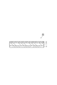
- FIG. 1 is a cross-sectional view showing a temporary protective film according to an embodiment.
- the temporary protective film 10 of FIG. 1 is provided on the support film 1, the adhesive layer 2 provided on one main surface of the support film 1, and on the other main surface of the support film 1 while being in contact with the support film 1. It has a non-adhesive layer 3 (a resin layer having substantially no adhesiveness).
- These temporary protective films are used on the back surface of the lead frame (the surface opposite to the surface on which the semiconductor element is mounted) in the sealing molding step of forming the sealing layer for sealing the semiconductor element mounted on the lead frame. ),
- the lead frame can be used as a temporary protective film for semiconductor sealing molding for temporary protection during sealing molding.
- the 90-degree peel strength between the adhesive layer and the lead frame when the temporary protective film is attached to the lead frame having the die pad and the inner lead so that the adhesive layer is in contact with the lead frame is At 25 ° C., it may be 5 N / m or more, 10 N / m or more, 50 N / m or more, 100 N / m or more, or 150 N / m or more.
- the peel strength after sticking is 5 N / m or more at 25 ° C
- the temporary protective film is hard to peel off from the lead frame, and the sealing resin gets into between the lead frame and the adhesive layer during sealing molding. The problem tends to be suppressed.
- the peel strength after application may be 2000 N / m or less, 1500 N / m or less, or 1000 N / m or less at 25 ° C.
- the peel strength after sticking is measured by peeling the temporary protective film in the 90 degree direction with respect to the lead frame according to, for example, the 90 degree peeling method of JIS Z 0237.
- the 90-degree peel strength when the temporary protective film is peeled off at a speed of 270 to 330 mm / min or 300 mm / min at 25 ° C. is a 90-degree peeling tester (manufactured by Tester Sangyo Co., Ltd.). Is measured using.
- the peel strength after application depends on the glass transition temperature (Tg) of the adhesive layer, the adhesive temperature, the material of the adherend, the wettability of the adhesive layer, and the like. Therefore, the conditions should be appropriately selected in consideration of the glass transition temperature (Tg) of the adhesive layer, the adhesive temperature, the material of the lead frame, the wettability of the adhesive layer, etc. so that the peel strength after application is 5 N / m or more. Can be done. Among these, the glass transition temperature (Tg) and the attachment (adhesion) temperature of the adhesive layer have a large influence on the peel strength. Usually, an adhesive temperature that is about 0 to 30 ° C. higher than the glass transition temperature (Tg) of the adhesive layer is adopted. Appropriate conditions may be determined in consideration of the material of the lead frame, the wettability of the adhesive layer, and the like.
- the conditions for adhering the temporary protective film and the lead frame in order to measure the peel strength after application may be used.
- the lead frame a copper lead frame, a copper lead frame coated with palladium, or a 42 alloy lead frame is used, (1) temperature 230 ° C., pressure 6 MPa, time 10 seconds, (2) temperature 350 ° C., pressure 3 MPa, It can be attached under any of the bonding conditions of (3) temperature 250 ° C., pressure 8 MPa, and time 10 seconds.
- the 90-degree peel strength between the adhesive layer and the lead frame immediately before the sealing step may be 5 N / m or more, 10 N / m or more, or 50 N / m or more at 25 ° C.
- the 90-degree peel strength immediately before the sealing step is 5 N / m or more at 25 ° C., problems such as the sealing resin getting into the lead frame and the adhesive layer during the sealing step are suppressed. Tend.
- immediately before the sealing step is performed before the sealing step and when all the steps performed before the sealing step are completed.
- a heating step of heating the lead frame with the temporary protective film may be performed before performing the sealing step.
- the heating temperature in the heating step is not particularly limited, but may be 100 ° C. or higher in order to improve the adhesive strength between the adhesive layer and the lead frame.
- the heating temperature may be 400 ° C. or lower from the viewpoint of heat resistance of the lead frame and the temporary protective film.
- the heating temperature may be 130 ° C. or higher and 350 ° C. or lower.
- the heating time is not particularly limited, but may be 10 seconds or more in order to sufficiently improve the adhesive strength between the adhesive layer and the lead frame.
- the heating time may be 1 minute or more and 2 hours or less.
- various steps before moving the above heating step to the sealing step (for example, curing step of adhesive such as silver paste (bonding step of semiconductor element), reflow connection step, wire bond step, etc.) It may be done by heating in.
- curing step of adhesive such as silver paste (bonding step of semiconductor element), reflow connection step, wire bond step, etc.
- heating is usually performed at 140 to 200 ° C. for 30 minutes to 2 hours in order to cure the adhesive used for bonding. Therefore, the above heating step can be performed by heating in these various steps.
- the temporary protective film is attached to the lead frame so that the adhesive layer is in contact with the lead frame, the semiconductor element is mounted on the surface of the die pad opposite to the temporary protective film, and the semiconductor element is sealed while being in contact with the adhesive layer.
- the 90-degree peel strength between the adhesive layer and the lead frame and the sealing layer (hereinafter, also referred to as “post-sealing peel strength”) is in the temperature range of 0 to 250 ° C. At least a part of the above may be 1000 N / m or less, 800 N / m or less, or 500 N / m or less.
- the peel strength after sealing When the peel strength after sealing is 1000 N / m or less, the problem of breakage tends to be suppressed when stress is applied to the lead frame and the sealing layer.
- the peel strength after sealing usually decreases as the measured temperature increases.
- the peel strength after sealing may be 0 N / m or more, 3 N / m or more, or 5 N / m or more in at least a part of the temperature range of 0 to 250 ° C.
- the peel strength after sealing may be in the above-mentioned range in at least a part of the temperature range of 80 to 250 ° C., and is in the above-mentioned range in the temperature at which the temporary protective film is peeled from the lead frame and the sealing layer. You can.
- the peel strength after sealing is 90 degrees in accordance with the 90 degree peeling method of JIS Z 0237, with a temporary protective film against the lead frame and sealing layer at room temperature or on a stage at 0 to 250 ° C. Peel off and measure.
- the 90 degree peel strength when peeling the temporary protective film at a speed of 270 to 330 mm / min or 300 mm / min is a 90 degree peeling tester. Measured using (manufactured by Testa Sangyo Co., Ltd.).
- the measurement temperature range of this peel strength may be 80 to 240 ° C. or 140 to 230 ° C.
- the temperature at which the temporary protective film is peeled off from the lead frame and the sealing layer may usually be between 0 and 250 ° C.
- the sealing conditions with the sealing material for measuring the peel strength after sealing in at least a part of the temperature range of 0 to 250 ° C. are not particularly limited, but the sealing layer in the method for manufacturing a semiconductor device described later is used. It may be a condition to be formed.
- CEL-9200 trade name, biphenyl sealing material manufactured by Hitachi Chemical Co., Ltd.
- the sealing layer is formed under the conditions of a temperature of 180 ° C., a pressure of 10 MPa, and a time of 3 minutes. It may include forming and curing the encapsulant forming the encapsulating layer by heating at 180 ° C. for 5 hours.
- the adhesive layer may contain a resin.
- the resin used to form the adhesive layer (hereinafter, also referred to as "resin (a)") is an amide group (-NHCO-), an ester group (-CO-O-), an imide group (-NR 2 , but R). each is -CO-), ether group (-O-) or a sulfone group (-SO 2 - may be a thermoplastic resin having a).
- the resin (a) may be a thermoplastic resin having an amide group, an ester group, an imide group or an ether group.
- the resin (a) include aromatic polyamide, aromatic polyester, aromatic polyimide, aromatic polyamideimide, aromatic polyether, aromatic polyetheramideimide, aromatic polyetheramide, aromatic polyesterimide and the like.
- Aromatic polyetherimides can be mentioned.
- the resin (a) may be at least one selected from the group consisting of aromatic polyetherimide imide, aromatic polyetherimide and aromatic polyetheramide.
- the resin (a) is obtained by polycondensing, for example, an aromatic diamine or bisphenol which is a basic component with a dicarboxylic acid, a tricarboxylic acid, a tetracarboxylic acid or an aromatic chloride which is an acid component, or a reactive derivative thereof.
- an aromatic diamine or bisphenol which is a basic component with a dicarboxylic acid, a tricarboxylic acid, a tetracarboxylic acid or an aromatic chloride which is an acid component, or a reactive derivative thereof.
- a usual method is used for the polycondensation reaction of an aromatic dicarboxylic acid, an aromatic tricarboxylic acid or a reactive derivative thereof with a diamine.
- Aromatic polyetherimide, aromatic polyetheramide imide and aromatic polyetheramide may contain a structural unit derived from a base component used for synthesizing these polymers.
- base component used for synthesizing these polymers.
- basic components include 2,2-bis [4- (4-aminophenoxy) phenyl] propane, bis [4- (4-aminophenoxy) phenyl] sulfone, 4,4'-diaminodiphenyl ether, and bis [4.
- Aromatic amines with ether groups such as-(4-aminophenoxy) phenyl] ether, 2,2-bis [4- (4-aminophenoxy)] hexafluoropropane; 4,4'-methylenebis (2,6-methylenebis) Aromatic diamines having no ether group such as diisopropylamine); siloxane diamines such as 1,3-bis (3-aminopropyl) -tetramethyldisiloxane; and 1,12-diaminododecane, 1,6-diaminohexane and the like. ⁇ , ⁇ -diaminoalkane can be mentioned.
- the proportion of aromatic diamines having an ether group is 40 to 100 mol% or 50 to 97 mol%, and aromatic diamines, siloxane diamines and ⁇ , ⁇ - without ether groups are used.
- the proportion of at least one selected from the diaminoalkanes may be in an amount of 0-60 mol%, or 3-50 mol%.
- combinations of base components include (1) 60 to 89 mol% or 68 to 82 mol% of aromatic diamine having an ether group, 1 to 10 mol% of siloxane diamine, or 3 to 7 mol%, and ⁇ .
- Aromatic polyetherimide, aromatic polyetheramide imide and aromatic polyetheramide may contain a structural unit derived from an acid component used for the synthesis of these polymers.
- the acid component include (A) reactive derivatives of trimellitic anhydride such as trimellitic anhydride, trimellitic anhydride chloride, mononuclear aromatic tricarboxylic acid anhydride or mononuclear such as pyromellitic dianhydride.
- Aromatic tetracarboxylic dianhydride (B) Bisphenol A bistrimericate dianhydride, Polynuclear aromatic tetracarboxylic dianhydride such as oxydiphthalic anhydride, (C) terephthalic acid, isophthalic acid, terephthalic acid chloride, Examples include aromatic dicarboxylic acids such as reactive derivatives of phthalic acid such as isophthalic anhydride.
- aromatic polyetheramide for example, 0.95 to 1.05 mol or 0.98 to 1.02 mol of the acid component (A) is reacted per 1 mol of the above-mentioned base component (1) or (2). It may be obtained by The aromatic polyetherimide is obtained by reacting, for example, 0.95 to 1.05 mol or 0.98 to 1.02 mol of the acid component (B) per 1 mol of the above-mentioned base component (3). It may be.
- the adhesive layer may contain a filler such as ceramic powder, glass powder, silver powder, copper powder, resin particles, rubber particles, a coupling agent, and the like.
- a filler such as ceramic powder, glass powder, silver powder, copper powder, resin particles, rubber particles, a coupling agent, and the like.
- the content of the filler may be 1 to 30 parts by weight or 5 to 15 parts by weight with respect to 100 parts by weight of the resin (a).
- the coupling agent may be, for example, vinylsilane, epoxysilane, mercaptosilane, titanate, aluminum chelate, zircoaluminate or a combination thereof.
- the coupling agent may be a silane coupling agent.
- silane coupling agents include vinyltrimethoxysilane, vinyltriethoxysilane, 2- (3,4-epoxycyclohexyl) ethyltrimethoxysilane, 3-glycidoxypropyltrimethoxysilane, 3-glycidoxypropyl.
- the silane coupling agent may be an epoxy silane coupling agent having an epoxy group.
- the adhesive layer contains a silane coupling agent, the adhesion of the adhesive layer to the support film can be improved, so that when the temporary protective film is peeled off, it is peeled off at the interface between the adhesive layer and the support film. Is less likely to occur.
- the content of the coupling agent may be 1 to 15 parts by weight or 2 to 10 parts by weight with respect to 100 parts by weight of the resin (a).
- the glass transition temperature of the adhesive layer may be 100 to 300 ° C, 130 to 280 ° C, or 150 to 250 ° C.
- the glass transition temperature is 100 ° C. or higher, when the temporary protective film is peeled off from the lead frame and the sealing material, peeling does not easily occur at the interface between the adhesive layer and the support film, and the adhesive layer tends to be less likely to coagulate and break. .. Further, in the wire bonding step, the adhesive layer does not soften too much, the dispersion of the force at the time of wire connection is suppressed, and the wire connection failure tends to be less likely to occur.
- the glass transition temperature is 300 ° C.
- the adhesive layer is sufficiently softened during bonding, so that a decrease in 90-degree peel strength between the adhesive layer and the lead frame at 25 ° C. tends to be suppressed. Therefore, leakage of the sealing material is unlikely to occur during peeling and sealing in the transport process.
- the 5% weight loss temperature of the adhesive layer may be 300 ° C. or higher, 350 ° C. or higher, or 400 ° C. or higher.
- the 5% weight loss temperature of the adhesive layer can be determined by measuring with a differential thermal balance (manufactured by Seiko Instruments Inc., TG / DTA220) at a heating rate of 10 ° C./min.
- the elastic modulus of the adhesive layer at 230 ° C. may be 1 MPa or more, or 3 MPa or more.
- the wire bond temperature is not particularly limited, but is generally about 180 to 260 ° C., and is often around 230 ° C. Therefore, when the elastic modulus at 230 ° C. is 1 MPa or more, the adhesive layer is not excessively softened by the heat in the wire bonding process, and there is a tendency that wire bonding failure does not easily occur.
- the upper limit of the elastic modulus of the adhesive layer at 230 ° C. is not particularly limited, but may be 2000 MPa or less, 1500 MPa or less, or 1000 MPa or less.
- a dynamic viscoelasticity measuring device (Rheogel-E4000, manufactured by UBM Co., Ltd.) at a distance between chucks of 20 mm, and has a sine wave, a temperature rise rate of 5 ° C./min, and a frequency of 10 Hz. Measured by the tensile mode of.
- the thickness (A) of the adhesive layer may be 1 to 20 ⁇ m, 3 to 15 ⁇ m, or 4 to 10 ⁇ m.
- the thickness (A) of the adhesive layer is 1 ⁇ m or more, the adhesiveness is excellent and the sealing material tends to be less likely to leak during sealing.
- the thickness (A) of the adhesive layer is 20 ⁇ m or less, it tends to be more economical.
- the support film is not particularly limited, but may be a film containing a resin (heat resistant resin) that can withstand heat during the coating, drying, and semiconductor device assembly processes of the resin used for forming the adhesive layer or the non-adhesive layer.
- Supporting films include, for example, aromatic polyimides, aromatic polyamides, aromatic polyamideimides, aromatic polysulfones, aromatic polyethersulfones, polyphenylene sulfides, aromatic polyetherketones, polyarylates, aromatic polyetheretherketones and polyethylenena. It may be a film of at least one polymer selected from the group consisting of phthalate, that is, a film containing the polymer.
- the glass transition temperature of the support film may be 200 ° C. or higher, or 250 ° C. or higher in order to improve heat resistance.
- the support film can be used in heat-applied steps such as a step of adhering a semiconductor element to a die pad, a wire bonding step, a sealing step, and a step of peeling a temporary protective film from a sealed molded body. Work can be done efficiently without softening.
- the coefficient of linear expansion of the support film at 20 to 200 ° C. is 3.0 ⁇ 10-5 / ° C. or less, 2.5 ⁇ 10 -5 / ° C. or less, or 2.0 ⁇ 10 -5 / °C may be less.
- the coefficient of linear expansion of the support film at 20 to 200 ° C. is performed according to JIS K 7197.
- the measurement uses a thermomechanical analyzer (TMA). The distance between the chucks is set to 20 mm, and the coefficient of thermal expansion at 20 to 200 ° C. is calculated.
- the heat shrinkage rate when the support film is heated at 200 ° C. for 2 hours is 0.15% or less and 0.13% or less. , Or 0.10% or less.
- the heat shrinkage rate can be measured according to JIS K 7133.
- a universal measuring microscope MF-U manufactured by Mitutoyo Co., Ltd. is used for measuring the heat shrinkage rate.
- the heat shrinkage rate can be determined by measuring the difference in dimensions of the support film before and after the heat treatment in the MD direction (longitudinal direction) or the TD direction (direction perpendicular to the MD direction).
- the heat treatment conditions are a temperature of 200 ° C. and a time of 2 hours.
- the heat shrinkage rate is a measured value in the larger of the MD direction and the TD direction.
- the support film may have sufficiently high adhesion to the adhesive layer. If the adhesiveness is high, when the temporary protective film is peeled off from the lead frame and the sealing material at a temperature of 100 to 300 ° C., peeling does not easily occur at the interface between the adhesive layer and the supporting film, and the lead frame and the sealing material are not easily peeled off. Resin does not easily remain on the surface.
- the support film may be a polyimide film from the viewpoint of heat resistance and adhesion to the adhesive layer.
- the support film may be surface-treated in order to sufficiently enhance the adhesion to the adhesive layer.
- the surface treatment method of the support film is not particularly limited, and examples thereof include chemical treatment such as alkali treatment and silane coupling treatment, physical treatment such as sand mat treatment, plasma treatment, and corona treatment.
- the thickness of the support film is not particularly limited, but may be 5 to 100 ⁇ m or 5 to 50 ⁇ m or less. When the thickness of the support film is 5 ⁇ m or more, the temporary protective film is less likely to wrinkle, so that workability tends to be high. When the thickness of the support film is 100 ⁇ m or less, the warp of the lead frame after the temporary protective film is attached to the lead frame tends to be suppressed.
- the material of the support film may be a metal selected from the group consisting of copper, aluminum, stainless steel and nickel.
- the support film contains these metals, the linear expansion coefficients of the lead frame and the support film are close to each other, so that the warp of the lead frame after the temporary protective film is attached to the lead frame can be reduced.
- the ratio T 2 / T 1 of the thickness T 2 of the adhesive layer to the thickness T 1 of the support film may be 0.5 or less, 0.3 or less, or 0.2 or less.
- T 2 / T 1 is 0.5 or less, curling of the film due to the volume reduction of the adhesive layer at the time of removing the solvent after coating is suppressed, and the workability when attaching to the lead frame tends to be high.
- the non-adhesive layer is a resin layer that does not substantially have adhesiveness (or pressure-sensitive adhesiveness) to the lead frame at 0 to 270 ° C.
- the volume of the adhesive layer is reduced when the solvent is removed, or the curl of the temporary protective film is caused by the volume reduction of the adhesive layer due to imidization and shrinkage during curing of the thermosetting resin. Can be offset.
- the non-adhesive layer may be a resin layer that does not easily soften at a high temperature.
- a resin layer having a high glass transition temperature can function as a non-adhesive layer.
- the non-adhesive layer may contain a resin.
- the composition of the resin used for forming the non-adhesive layer (hereinafter, also referred to as “resin (b)”) is not particularly limited, and may be either a thermoplastic resin or a thermosetting resin.
- the thermoplastic resin is not particularly limited, but may be a thermoplastic resin having at least one functional group selected from the group consisting of an amide group, an ester group, an imide group, an ether group and a sulfone group.
- the thermosetting resin is not particularly limited, and may be, for example, an epoxy resin, a phenol resin, a bismaleimide resin (for example, a bismaleimide resin having bis (4-maleimidephenyl) methane as a monomer) or the like.
- a thermoplastic resin and a thermosetting resin may be combined.
- the amount of the thermosetting resin may be 5 to 100 parts by mass or 20 to 70 parts by mass with respect to 100 parts by mass of the thermoplastic resin.
- the non-adhesive layer may contain a filler such as ceramic powder, glass powder, silver powder, copper powder, resin particles, rubber particles, a coupling agent, and the like.
- a filler such as ceramic powder, glass powder, silver powder, copper powder, resin particles, rubber particles, a coupling agent, and the like.
- the content of the filler may be 1 to 30 parts by mass with respect to 100 parts by mass of the resin (b), and may be 5 to 15 parts by mass.
- the content of the coupling agent may be 1 to 20 parts by mass and 2 to 15 parts by mass with respect to 100 parts by mass of the resin (b).
- the elastic modulus of the non-adhesive layer at 230 ° C. may be 10 MPa or more, 100 MPa or more, or 1000 MPa or more.
- the elastic modulus of the non-adhesive layer at 230 ° C. may be 2000 MPa or less, or 1500 MPa or less.
- the elastic modulus of the non-adhesive layer at 230 ° C. is set in a dynamic viscoelasticity measuring device (Rheogel-E4000, manufactured by UBM Co., Ltd.) at a distance between chucks of 20 mm, and has a sine wave, a temperature rise rate of 5 ° C./min, and a frequency. It can be measured in a 10 Hz tensile mode.
- a dynamic viscoelasticity measuring device Heogel-E4000, manufactured by UBM Co., Ltd.
- the adhesive strength of the non-adhesive layer to the mold and the jig is not particularly limited as long as it is low enough not to stick to the mold and / or the jig in the process, but between the non-adhesive layer and the mold and the jig at 25 ° C.
- the 90 degree peel strength of is less than 5 N / m, or less than 1 N / m. This peel strength is measured, for example, after crimping a brass die at a temperature of 250 ° C. and a pressure of 8 MPa for 10 seconds.
- the glass transition temperature of the non-adhesive layer is difficult to soften in the process of adhering the semiconductor element to the die pad, the wire bonding process, the sealing process, the process of peeling the temporary protective film from the encapsulating molded body, etc., and the mold and jig
- the temperature may be 150 ° C. or higher, 200 ° C. or higher, or 250 ° C. or higher in order to prevent sticking to.
- the glass transition temperature of the non-adhesive layer may be 350 ° C. or lower, or 300 ° C. or lower.
- the thickness of the non-adhesive layer may be, for example, 10 ⁇ m or less, 9 ⁇ m or less, 8 ⁇ m or less, or 7 ⁇ m or less.
- the thickness of the non-adhesive layer may be, for example, 1 ⁇ m or more, 2 ⁇ m or more, 3 ⁇ m or more, 4 ⁇ m or more, 5 ⁇ m or more, or 6 ⁇ m or more.
- the thickness of the non-adhesive layer is not particularly limited, but may be, for example, 1 to 10 ⁇ m or 1 to 8 ⁇ m.
- the surface roughness Ra of the surface of the non-adhesive layer opposite to the surface in contact with the support film may be 0.1 ⁇ m, 0.15 ⁇ m or more, or 0.2 ⁇ m or more.
- the surface roughness Ra here is a value measured by a laser microscope under the condition of a magnification of 50 times that of the objective lens.
- the surface roughness Ra is obtained, for example, by analyzing an image in which images of 11 vertical sections and 9 horizontal sections are connected.
- the surface roughness Ra is 0.1 ⁇ m or more, it is excellent in sliding with the stage in the apparatus, less likely to cause jamming problems, and also excellent in sliding between lead frames to which a temporary protective film is attached. , It is hard to cause a problem that it sticks and cannot be peeled off.
- the surface roughness Ra can be measured with a shape measurement laser microscope VK-X100 manufactured by KEYENCE CORPORATION, which is a laser microscope.
- the surface roughness (Ra) of the surface of the non-adhesive layer opposite to the surface in contact with the support film may be, for example, 3 ⁇ m or less, 2 ⁇ m or less, or 1 ⁇ m or less.
- the surface roughness Ra of the surface of the non-adhesive layer opposite to the surface in contact with the support film is 0.4 ⁇ m or more when measured by a laser microscope under the condition of 10 times the magnification of the objective lens. , 0.5 ⁇ m or more, or 0.6 ⁇ m or more, and may be 8 ⁇ m or less, or 6 ⁇ m or less.
- the resin (a) used for forming the adhesive layer is used as a solvent such as N-methyl-2-pyrrolidone, dimethylacetamide, diethylene glycol dimethyl ether, tetrahydrofuran, cyclohexanone, methyl ethyl ketone, and dimethylformamide.
- a solvent such as N-methyl-2-pyrrolidone, dimethylacetamide, diethylene glycol dimethyl ether, tetrahydrofuran, cyclohexanone, methyl ethyl ketone, and dimethylformamide.
- the method for forming the temporary protective film is to prepare a precursor varnish in which a resin (a) precursor (for example, polyamic acid) that produces a resin (a) (for example, polyimide resin) by heat treatment or the like is dissolved in a solvent. It may include coating one side of the support film with the precursor varnish and forming an adhesive layer containing the resin (a) by heat-treating the coated precursor varnish. Also by this method, a temporary protective film having a two-layer structure can be obtained. When the resin (a) precursor is used, the solvent is removed by heat treatment after coating, and the resin (a) is produced from the precursor by, for example, imidization. An adhesive varnish may be used from the viewpoint of the surface condition of the coated surface and the like.
- a resin (a) precursor for example, polyamic acid
- a resin (a) for example, polyimide resin
- the temperature of the heat treatment may differ depending on whether an adhesive varnish is used or a precursor varnish is used.
- the temperature may be such that the solvent can be removed, and in the case of the precursor varnish, the treatment temperature may be higher than the glass transition temperature of the adhesive layer for imidization.
- the varnish can be applied using a roll coat, a reverse roll coat, a gravure coat, a bar coat, or a comma coat.
- These varnishes may be applied by passing a support film through an adhesive varnish or a precursor varnish.
- the method for forming the non-adhesive layer is not particularly limited, but for example, the resin (b) is dissolved in a solvent such as N-methyl-2-pyrrolidone, dimethylacetamide, diethylene glycol dimethyl ether, tetrahydrofuran, cyclohexanone, methyl ethyl ketone, and dimethylformamide.
- a solvent such as N-methyl-2-pyrrolidone, dimethylacetamide, diethylene glycol dimethyl ether, tetrahydrofuran, cyclohexanone, methyl ethyl ketone, and dimethylformamide.
- the method of forming the non-adhesive layer is to prepare a precursor varnish by dissolving a resin (b) precursor (for example, polyamic acid) that produces a resin (b) (for example, a polyimide resin) by heating or the like in a solvent. It may include coating the precursor varnish on the support film and heating the coated precursor varnish. In this case, the solvent is removed by heat treatment after coating, and the resin (b) is produced from the precursor by, for example, imidization.
- a resin varnish may be used from the viewpoint of the surface condition of the coating film and the like.
- the temperature of the heat treatment may differ depending on whether a resin varnish is used or a precursor varnish is used.
- the temperature may be such that the solvent can be removed, and when a precursor varnish is used, the treatment temperature may be higher than the glass transition temperature of the non-adhesive layer for imidization.
- the varnish can be applied using a roll coat, a reverse roll coat, a gravure coat, a bar coat, a comma coat, or the like. These varnishes may be applied by passing a support film through a resin varnish or a precursor varnish.
- a semiconductor device can be manufactured by a method including a sealing molding step of a semiconductor element using a temporary protective film according to an embodiment.
- the semiconductor device includes, for example, a temporary protective film, a lead frame bonded to the adhesive layer of the temporary protective film, a semiconductor element bonded to a die pad of the lead frame, a wire connecting the semiconductor element and the inner lead of the lead frame, or It is manufactured by peeling the temporary protective film from a conductive material such as a metal plate and a semiconductor device with a temporary protective film provided with an exposed surface of a lead frame, a semiconductor element, and a sealing layer for sealing a wire.
- the manufactured semiconductor device has, for example, a lead frame, a semiconductor element mounted on the lead frame, and a sealing layer for sealing the semiconductor element on the semiconductor element side of the lead frame, and the back surface of the lead frame is for external connection. It may be a Non Lead Type Package that is exposed to the surface. Specific examples thereof include QFN (QuadFlat Non-readed Package) and SON (Small Outline Non-readed Package).
- FIGS. 2 and 3 are cross-sectional views showing a method of manufacturing a semiconductor device according to an embodiment.
- FIG. 4 is a cross-sectional view showing an embodiment of a semiconductor device obtained by the manufacturing methods of FIGS. 2 and 3.
- each process will be described with reference to each drawing as necessary.
- the method for manufacturing a semiconductor device includes a step of attaching a temporary protective film 10 to one side (back surface) of a lead frame 11 having a die pad 11a and an inner lead 11b so that the adhesive layer is in contact with the lead frame, and a die pad.
- the steps are provided in this order.
- the temporary protective film 10 may be attached to the lead frame 11 under heating, or at room temperature (for example, 5 to 35 ° C.).
- the method of pasting is not particularly limited, but may be, for example, a roll laminating method.
- the lead frame with a temporary protective film according to one embodiment includes a lead frame 11 having a die pad 11a and an inner lead 11b, and a temporary protective film 10.
- the temporary protective film 10 is attached to the lead frame 11 so that the adhesive layer 2 is in contact with one side of the lead frame 11.
- the conditions for adhering the temporary protective film 10 to the lead frame 11 are not particularly limited, but the adhesive temperature may be 150 to 400 ° C, 180 to 350 ° C, or 200 to 300 ° C.
- the bonding temperature is 150 ° C. or higher, the bonding strength between the lead frame 11 and the bonding layer 2 tends to be further improved.
- the bonding temperature is 400 ° C. or lower, the deterioration of the lead frame 11 tends to be further suppressed.
- the adhesive pressure of the temporary protective film 10 to the lead frame 11 may be 0.5 to 30 MPa, 1 to 20 MPa, or 3 to 15 MPa.
- the adhesive pressure is 0.5 MPa or more, the adhesive strength between the adhesive layer 2 and the lead frame 11 tends to be further improved.
- the adhesive pressure is 30 MPa or less, damage to the lead frame 11 tends to be more easily suppressed.
- the adhesion time of the temporary protective film 10 to the lead frame 11 may be 0.1 to 60 seconds, 1 to 30 seconds, or 3 to 20 seconds.
- the bonding time is 0.1 seconds or more, the bonding strength between the bonding layer 2 and the lead frame 11 tends to be further improved.
- the bonding time is 60 seconds or less, workability and productivity tend to be improved more easily.
- Preheating may be performed for about 5 to 60 seconds before applying pressure.
- the material of the lead frame 11 is not particularly limited, but may be, for example, an iron-based alloy such as 42 alloy, copper, or a copper-based alloy. When copper and a copper-based alloy are used, the surface of the lead frame may be coated with palladium, gold, silver or the like.
- the semiconductor element 14 is usually mounted (adhered) to the die pad 11a via an adhesive (for example, silver paste).
- the adhesive may be cured by heat treatment (for example, 140 to 200 ° C., 30 minutes to 2 hours).
- the semiconductor element and the inner lead may be connected by solder reflow using a conductive material such as a copper plate. That is, the method of manufacturing a semiconductor device may further include a step of connecting the semiconductor element mounted on the die pad and the inner lead with a conductive material by reflow.
- the reflow connection may be performed, for example, in a temperature range of a maximum temperature of 250 to 420 ° C. and for 1 to 30 minutes.
- the connection by reflow is performed, for example, before the step of obtaining the sealed molded body 20 and after the step of mounting (adhering) the semiconductor element 14.
- the connection by reflow may be performed, for example, after the step of mounting (adhering) the semiconductor element 14 and before the step of providing the wire 12.
- the wire 12 is not particularly limited, but may be, for example, a gold wire, a copper wire, a palladium-coated copper wire, or an aluminum wire.
- the semiconductor element and the inner lead may be joined to the wire 12 by heating at 200 to 300 ° C. for 3 minutes to 3 hours.
- the sealing layer 13 is formed using the sealing material.
- a sealing molded body 20 having a plurality of semiconductor elements 14 and a sealing layer 13 for collectively sealing them can be obtained. Since the temporary protective film 10 is provided during the sealing molding, it is possible to prevent the sealing material from wrapping around to the back surface side of the lead frame 11.
- the sealing molded body with a temporary protective film connects a lead frame 11 having a die pad 11a and an inner lead 11b, a semiconductor element 14 mounted on the die pad 11a, and the semiconductor element 14 and the inner lead 11b.
- a wire 12, a sealing layer 13 that seals the semiconductor element 14 and the wire 12, and a temporary protective film 10 are provided.
- the temporary protective film 10 is attached to the surface of the lead frame 11 whose adhesive layer 2 is opposite to the surface on which the semiconductor element 14 is mounted.
- the temperature (sealing temperature) during the formation of the sealing layer 13 may be, for example, 150 to 200 ° C.
- the pressure (sealing pressure) during the formation of the sealing layer may be 6 to 15 MPa or 7 to 10 MPa.
- the heating time (sealing time) in the sealing molding may be 1 to 5 minutes or 2 to 3 minutes.
- the formed sealing layer 13 may be heat-cured if necessary.
- the heating temperature for curing the sealing layer 13 (sealing curing temperature) may be 150 to 200 ° C.
- the heating time for curing the sealing layer 13 may be, for example, 4 to 6 hours.
- the encapsulant is not particularly limited, but may be a curable resin composition containing an epoxy resin such as a cresol novolac epoxy resin, a phenol novolac epoxy resin, a biphenyl diepoxy resin, or a naphthol novolac epoxy resin.
- the encapsulant may contain, for example, a flame-retardant substance such as a filler or a brom compound, or an additive such as a wax component.
- the temporary protective film 10 is peeled off from the lead frame 11 and the sealing layer 13 of the obtained sealing molded body 20.
- the temporary protective film 10 may be peeled off at any time before or after the curing of the sealing layer 13.
- the temperature at which the temporary protective film 10 is peeled from the sealed molded product may be between 0 and 250 ° C.
- peeling temperature When the peeling temperature is 0 ° C. or higher, the adhesive layer is less likely to remain on the lead frame 11 and the sealing layer 13.
- the peeling temperature When the peeling temperature is 250 ° C. or lower, deterioration of the lead frame 11 and the sealing layer 13 tends to be more easily suppressed.
- the peeling temperature may be 80-240 ° C or 140-230 ° C.
- the method for manufacturing the semiconductor device may further include a step of removing the adhesive layer (adhesive residue) remaining on the lead frame 11 and the sealing layer 13 after the peeling step.
- the adhesive layer 2 may not remain on the lead frame 11 and the sealing layer 13.
- the adhesive layer remaining on the lead frame 11 and the sealing layer 13 may be removed by mechanical brushing, a solvent, or the like.
- the solvent is not particularly limited, and may be, for example, N-methyl-2-pyrrolidone, dimethylacetamide, diethylene glycol dimethyl ether, tetrahydrofuran, cyclohexanone, methylethylketone, dimethylformamide, or a combination thereof.
- the encapsulating molded body 20 may be divided to obtain a plurality of semiconductor devices 100 of FIG. 4 each having one semiconductor element, if necessary. it can.
- the manufacturing method according to one embodiment is to enclose the temporary protective film 10 from the sealing molded body 20.
- a step of dividing the sealing molded body 20 before or after peeling to obtain a semiconductor device 100 having one die pad 11a and a semiconductor element 14 may be further provided.
- a semiconductor device may be manufactured by winding a long temporary protective film around a winding core and unwinding the temporary protective film from the obtained reel body.
- the reel body in this case has a winding core and a temporary protective film wound around the winding core according to the above-described embodiment.
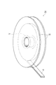
- FIG. 6 is a perspective view showing an embodiment of the reel body.
- the reel body 30 shown in FIG. 6 includes a winding core 31, a temporary protective film 10 wound around the winding core 31, and a side plate 32.
- the width of the winding core 31 and the temporary protective film 10 may be, for example, 10 mm or more, 40 mm or more, 60 mm or more, or 80 mm or more, and may be 350 mm or less.
- the width of the winding core 31 and the temporary protective film 10 (the length in the direction orthogonal to the winding direction) may be, for example, 10 mm or more and 350 mm or less, 40 mm or more and 350 mm or less, or 80 mm or more and 350 mm or less.
- the temporary protective film according to the above-described embodiment may be provided as a packaging body in which the reel body is housed in a packaging bag.
- FIG. 7 shows an embodiment of the package.
- the packaging body 50 includes the reel body 30 and a packaging bag 40 containing the reel body 30.
- the reel bodies 30 are usually individually housed in a packaging bag, but a plurality of (for example, 2 to 3) reel bodies 30 may be housed in one packaging bag 40.
- the packaging bag 40 may be formed of a resin film, or may be formed of a composite film which is a resin film having an aluminum layer. Specific examples of the packaging bag 40 include an aluminum-coated plastic bag and the like. Examples of the material of the resin film include plastics such as polyethylene, polyester, vinyl chloride, and polyethylene terephthalate.
- the reel body 30 may be housed in a packaging bag in a vacuum-packed state, for example.
- the package 50 is not limited to the vacuum-packed one.
- the packaging bag 40 may contain a desiccant together with the reel body 30.
- the desiccant include silica gel.
- the packaging body 50 may be a packaging bag 40 containing the reel body 30 further wrapped with a cushioning material.
- the package 50 may be provided as a package housed in a package box.
- FIG. 8 shows an embodiment of the package.
- the package 70 includes the package 50 and a packaging box 60 containing the package 50.
- the packing box 60 contains one or more packaging bodies 50.
- the packing box 60 for example, corrugated cardboard can be used.
- the semiconductor device manufactured by using the temporary protective film according to one embodiment is excellent in terms of high density, small area, thinning, and the like.
- electronic devices such as mobile phones, smartphones, personal computers, and tablets. Can be suitably used for.
- Varnish A-1 (varnish for forming adhesive layer) 270.9 g (0.) Propane 2,2-bis [-(4-aminophenoxy) phenyl] propane in a 5-liter four-necked flask equipped with a thermometer, agitator, nitrogen introduction pipe and fractional distillation tower under a nitrogen atmosphere. 66 mol), 8.7 g (0.035 mol) of 1,3-bis (3-aminopropyl) -tetramethyldisiloxane was added, and this was dissolved in 1950 g of N-methyl-2-pyrrolidone. The solution was cooled to 0 ° C.
- trimellitic anhydride chloride 149.5 g (0.71 mol) of trimellitic anhydride chloride was added to the solution at this temperature.
- 100 g of triethylamine was added to the solution.
- the temperature was raised to 180 ° C. and the reaction for 5 hours completed imidization.
- the reaction solution was put into methanol to precipitate a polymer.
- the precipitated polymer was dried and then dissolved in N-methyl-2-pyrrolidone.
- the solution was poured into methanol to precipitate the polymer again.
- the precipitated polymer was dried under reduced pressure to obtain a purified powdery polyetheramideimide.
- Varnish A-2 (Varnish for forming an adhesive layer) 258.6 g (0) of 2,2-bis [4- (4-aminophenoxy) phenyl] propane in a 5-liter four-necked flask equipped with a thermometer, agitator, nitrogen introduction pipe and fractional distillation tower under a nitrogen atmosphere. .63 mol), 1,3-bis (3-aminopropyl) tetramethyldisiloxane 67.0 g (0.27 mol) was added, and this was dissolved in 1550 g of N-methyl-2-pyrrolidone.
- the solution was cooled to 0 ° C., and 187.3 g (0.89 mol) of trimellitic anhydride chloride was added to the solution at this temperature.
- trimellitic acid chloride was dissolved, 100 g of triethylamine was added to the solution.
- the temperature was raised to 180 ° C. and the reaction for 5 hours completed imidization.
- the reaction solution was put into methanol to precipitate a polymer.
- the precipitated polymer was dried and then dissolved in N-methyl-2-pyrrolidone.
- the solution was poured into methanol to precipitate the polymer again.
- the precipitated polymer was dried under reduced pressure to obtain a purified powdery polyetheramideimide.
- Varnish B-1 (varnish for forming a non-adhesive layer) 172.4 g (0) of 2,2-bis [4- (4-aminophenoxy) phenyl] propane in a 5-liter four-necked flask equipped with a thermometer, a stirrer, a nitrogen introduction tube and a fractionation tower under a nitrogen atmosphere. .42 mol), 153.7 g (0.42 mol) of 4,4′-methylenebis (2,6-diisopropylaniline) was added, and this was dissolved in 1550 g of N-methyl-2-pyrrolidone.
- the solution was cooled to 0 ° C., and 174.7 g (0.83 mol) of trimellitic anhydride chloride was added to the solution at this temperature.
- trimellitic acid chloride was dissolved, 130 g of triethylamine was added to the solution.
- the temperature was raised to 180 ° C. and the reaction for 5 hours completed imidization.
- the reaction solution was put into methanol to precipitate a polymer.
- the precipitated polymer was dried and then dissolved in N-methyl-2-pyrrolidone.
- the solution was poured into methanol to precipitate the polymer again.
- the precipitated polymer was dried under reduced pressure to obtain a purified powdery polyetheramideimide.
- Varnish B containing 120 g of the obtained polyether amide imide and 6 g of a silane coupling agent (trade name: SH6040 manufactured by Shin-Etsu Chemical Industry Co., Ltd.) dissolved in 360 g of N-methyl-2-pyrrolidone and containing an aromatic polyether amide imide. I got -1.
- a silane coupling agent trade name: SH6040 manufactured by Shin-Etsu Chemical Industry Co., Ltd.
- Varnish B-2 (varnish for forming a non-adhesive layer) 40 g of the polyether amide imide synthesized in Production Example 3 and 2 g of a silane coupling agent (manufactured by Shinetsu Chemical Industry Co., Ltd., trade name: SH6040) were dissolved in 500 g of N-methyl-2-pyrrolidone to obtain an aromatic polyether amide imide. A varnish B-2 containing was obtained.
- Example 1 A polyimide film having a thickness of 25 ⁇ m (Kapton 100EN, manufactured by Toray DuPont Co., Ltd.) was used as a support film. Varnish A-1 was cast on one side of this polyimide film to a thickness of 25 ⁇ m. The coating film was dried at 100 ° C. for 10 minutes and at 300 ° C. for 10 minutes to obtain a temporary protective film having an adhesive layer having a thickness of 3 ⁇ m on one side of the support film. The adhesive layer was a layer having a glass transition temperature of 230 ° C., a 5% weight loss temperature of 451 ° C., and an elastic modulus of 150 MPa at 230 ° C.
- the varnish B-1 was poured to a thickness of 20 ⁇ m on the surface opposite to the surface on which the adhesive layer of the polyimide film was provided.
- the coating film was dried at 100 ° C. for 10 minutes and at 300 ° C. for 10 minutes to form a non-adhesive layer having a thickness of 2 ⁇ m.
- This non-adhesive layer was a layer having a glass transition temperature of 260 ° C., a 5% weight loss temperature of 421 ° C., and an elastic modulus of 1700 MPa at 230 ° C. As a result, as shown in FIG.
- Example 1 a temporary protective film of Example 1 in which an adhesive layer was provided on one surface of the support film and a non-adhesive layer was provided on the other surface was obtained.
- the ratio of the thickness (A) of the adhesive layer to the thickness (C) of the support film was 0.12.
- the surface roughness (Ra) of the surface (the back surface of the temporary protective film) opposite to the surface of the non-adhesive layer in contact with the support film is 0.26 ⁇ m under condition 1 and 0 under condition 2. It was 0.6 ⁇ m.
- the temporary protective film of Example 1 was adhered to a copper lead frame (50 mm ⁇ 200 mm) coated with palladium at a temperature of 250 ° C., a pressure of 8 MPa, and a time of 10 seconds, and a 90-degree peel strength between the adhesive layer and the lead frame at 25 ° C.
- peeling speed 300 mm per minute, the same applies hereinafter
- FIG. 5 is a schematic view showing a method for evaluating warpage. As shown in FIG. 5, a lead frame with a temporary protective film to which the temporary protective film 10 is attached to the lead frame 11 is placed on a table 200, and the warp (X) of the lead frame with the temporary protective film in the longitudinal direction is measured. It was measured. As a result of measuring the warp (X) by the temporary protective film of Example 1, the warp (X) was about 0.1 mm.
- the obtained package has the structure shown in FIG.
- a silver paste was used to bond the semiconductor elements, and the silver paste was cured by heating at 150 ° C. for 60 minutes.
- the wire bond was carried out by using a gold wire as a wire and heating at 260 ° C. for 5 minutes.
- a biphenyl encapsulant (manufactured by Hitachi Kasei Co., Ltd., trade name: CEL9200) was used as the encapsulant in the encapsulation step.
- a sealing layer was formed at a temperature of 180 ° C., a pressure of 10 MPa, and a time of 3 minutes, and then the sealing layer was cured by heating at 180 ° C. for 5 hours. No problem occurred in any of the steps.
- the 90 degree peel strength was 150 N / m and it could be easily peeled off, and the resin remained almost on the lead frame and the sealing resin. I didn't. A very small amount of residual resin could also be removed by washing with N-methyl-2-pyrrolidone. Further, this package was divided to produce a package having one semiconductor element each as shown in FIG. There were no problems during the process.
- Example 2 A polyimide film having a thickness of 25 ⁇ m (UPILEX SPA manufactured by Ube Industries, Ltd.) was used as a support film. Varnish A-1 was cast on one side of this polyimide film to a thickness of 40 ⁇ m. The coating film was dried at 100 ° C. for 10 minutes and at 300 ° C. for 10 minutes to obtain a temporary protective film having an adhesive layer having a thickness of 6 ⁇ m on one side of the support film. The adhesive layer was a layer having a glass transition temperature of 230 ° C., a 5% weight loss temperature of 451 ° C., and an elastic modulus of 150 MPa at 230 ° C.
- UPILEX SPA manufactured by Ube Industries, Ltd.
- the varnish B-2 was poured to a thickness of 100 ⁇ m on the surface opposite to the surface on which the adhesive layer of the polyimide film was provided.
- the coating film was dried at 100 ° C. for 10 minutes and at 300 ° C. for 10 minutes to form a non-adhesive layer having a thickness of 5 ⁇ m.
- This non-adhesive layer was a layer having a glass transition temperature of 260 ° C., a 5% weight loss temperature of 421 ° C., and an elastic modulus of 1700 MPa at 230 ° C. As a result, as shown in FIG.
- the temporary protective film of Example 2 in which the adhesive layer was provided on one surface of the support film and the non-adhesive layer was provided on the other surface was obtained.
- the ratio of the thickness (A) of the adhesive layer to the thickness (C) of the support film was 0.24.
- the surface roughness (Ra) of the surface (the back surface of the temporary protective film) opposite to the surface of the non-adhesive layer in contact with the support film is 0.22 ⁇ m under condition 1 and 0 under condition 2. It was 0.8 ⁇ m.
- Example 3 A polyimide film having a thickness of 25 ⁇ m (UPILEX SGA, manufactured by Ube Industries, Ltd.) was used as a support film. Varnish A-1 is cast on one side of this polyimide film to a thickness of 60 ⁇ m, dried at 100 ° C. for 10 minutes and at 300 ° C. for 10 minutes, and an adhesive layer having a thickness of 9 ⁇ m is provided on one side of the support film. A temporary protective film was obtained. The adhesive layer had an elastic modulus of 150 MPa at a glass transition temperature of 230 ° C., a 5% weight loss temperature of 451 ° C., and 230 ° C.
- the varnish B-2 for forming the non-adhesive layer produced in Production Example 2 was poured to a thickness of 180 ⁇ m on the surface opposite to the surface on which the adhesive layer of the polyimide film was provided, and 100 It was dried at ° C. for 10 minutes and at 300 ° C. for 10 minutes to form a non-adhesive layer having a thickness of 9 ⁇ m.
- the glass transition temperature of this non-adhesive layer was 260 ° C.
- the 5% weight loss temperature was 421 ° C.
- the elastic modulus at 230 ° C. was 1700 MPa.
- the temporary protective film of Example 3 in which the adhesive layer was provided on one surface of the support film and the non-adhesive layer was provided on the other surface was obtained.
- the ratio of the thickness (A) of the adhesive layer to the thickness (C) of the support film was 0.36.
- the surface roughness (Ra) of the surface (the back surface of the temporary protective film) opposite to the surface of the non-adhesive layer in contact with the support film is 0.67 ⁇ m under condition 1 and 1 under condition 2. It was .1 ⁇ m.
- Comparative Example 1 As the support film, a polyimide film (UPIREX SPA manufactured by Ube Industries, Ltd.) having a 25 ⁇ m-thick surface subjected to plasma treatment was used. Varnish A-2 was cast on one side of this polyimide film to a thickness of 50 ⁇ m. The coating film was dried at 100 ° C. for 10 minutes and at 300 ° C. for 10 minutes to form an adhesive layer having a thickness of 10 ⁇ m. This adhesive layer was a layer having a glass transition temperature of 187 ° C., a 5% weight loss temperature of 429 ° C., and an elastic modulus of 5 MPa at 230 ° C.
- UPIREX SPA manufactured by Ube Industries, Ltd.
- varnish B-1 was cast on the opposite surface of the polyimide film to a thickness of 50 ⁇ m.
- the coating film was dried at 100 ° C. for 10 minutes and at 300 ° C. for 10 minutes to form a non-adhesive layer having a thickness of 10 ⁇ m.
- This non-adhesive layer was a layer having an elastic modulus of 1700 MPa at a glass transition temperature of 260 ° C. and a 5% weight loss temperature of 421 ° C. and 230 ° C.
- a temporary protective film of Comparative Example 1 in which an adhesive layer was provided on one surface of the support film and a non-adhesive layer was provided on the other surface was obtained.
- the surface roughness (Ra) of the surface (the back surface of the temporary protective film) opposite to the surface of the non-adhesive layer in contact with the support film is 0.05 ⁇ m under condition 1 and 0 under condition 2. It was .3 ⁇ m.
- the semiconductor element bonding, wire bonding step, and sealing step were performed in the same manner as in Example 1, but the lead frame and the stage slipped in the lead frame transfer step. Due to the bad condition, a transportation problem was seen.
- the temporary protective film of the example in which the surface roughness (Ra) of the back surface is 0.1 ⁇ m or more under condition 1 and 0.4 ⁇ m or more under condition 2 has high adhesion to the lead frame at 25 ° C. and is sealed with a resin. Since it can be peeled off from the lead frame and the sealing material after being stopped, the semiconductor package can be manufactured with high workability and productivity.
- the semiconductor adhesive film of the comparative example in which the surface roughness (Ra) of the back surface is less than 0.1 ⁇ m under condition 1 and less than 0.4 ⁇ m under condition 2 has poor slippage on the stage in the semiconductor assembly process. Transport defects are observed, and workability and productivity are inferior to those of the temporary protective film of the example.
- Comparative Example 2 A polyimide film having a thickness of 25 ⁇ m (UPILEX SPA manufactured by Ube Industries, Ltd.) was used as a support film. Varnish A-1 was cast on one side of this polyimide film to a thickness of 40 ⁇ m. The coating film was dried at 100 ° C. for 10 minutes and at 300 ° C. for 10 minutes to obtain a temporary protective film having an adhesive layer having a thickness of 6 ⁇ m on one side of the support film. The adhesive layer was a layer having a glass transition temperature of 230 ° C., a 5% weight loss temperature of 451 ° C., and an elastic modulus of 150 MPa at 230 ° C.
- the varnish B-1 was poured to a thickness of 35 ⁇ m on the surface opposite to the surface on which the adhesive layer of the polyimide film was provided.
- the coating film was dried at 100 ° C. for 10 minutes and at 300 ° C. for 10 minutes to form a non-adhesive layer having a thickness of 5 ⁇ m.
- This non-adhesive layer was a layer having an elastic modulus of 1700 MPa at a glass transition temperature of 260 ° C. and a 5% weight loss temperature of 421 ° C. and 230 ° C. As a result, as shown in FIG.
- a temporary protective film of Comparative Example 2 in which an adhesive layer was provided on one surface of the support film and a non-adhesive layer was provided on the other surface was obtained.
- the ratio of the thickness (A) of the adhesive layer to the thickness (C) of the support film was 0.24.
- the surface roughness (Ra) of the surface (the back surface of the temporary protective film) opposite to the surface of the non-adhesive layer in contact with the support film is 0.06 ⁇ m under condition 1 and 0 under condition 2. It was .3 ⁇ m.
- the temporary protective film of the example had a lower maximum stress value in the friction test than the temporary protective film of the comparative example.
- the temporary protective film of Example 1 When the temporary protective film of Example 1 was used, it was confirmed that there was no transport defect.
- the temporary protective film of Comparative Example 1 when the temporary protective film of Comparative Example 1 was used, a transport problem occurred. It can be said that even in the case of the temporary protective films of Examples 1 and 2 showing the maximum stress value equal to or less than the maximum stress value of the temporary protective film of Example 1 in the friction test, the transfer failure is sufficiently suppressed.
Landscapes
- Chemical & Material Sciences (AREA)
- Organic Chemistry (AREA)
- Chemical Kinetics & Catalysis (AREA)
- Engineering & Computer Science (AREA)
- Mechanical Engineering (AREA)
- Health & Medical Sciences (AREA)
- Medicinal Chemistry (AREA)
- Polymers & Plastics (AREA)
- Encapsulation Of And Coatings For Semiconductor Or Solid State Devices (AREA)
- Adhesive Tapes (AREA)
- Laminated Bodies (AREA)
Abstract
Description
(2)ダイパッドの仮保護フィルムとは反対側の面上に半導体素子を搭載又は接着する工程、
(3)半導体素子とインナーリードとを接続するワイヤを設ける工程、
(4)半導体素子及びワイヤを封止する封止層を形成して、リードフレーム、半導体素子及び封止層を有する封止成形体を得る工程、及び
(5)封止成形体から仮保護フィルムを剥離する工程。
図1は、一実施形態に係る仮保護フィルムを示す断面図である。図1の仮保護フィルム10は、支持フィルム1と、支持フィルム1の一方の主面上に設けられた接着層2と、支持フィルム1の他方の主面上に、支持フィルム1に接しながら設けられた非接着層3(実質的に接着性を有しない樹脂層)とを有する。これらの仮保護フィルムは、リードフレームに搭載された半導体素子を封止する封止層を形成する封止成形の工程において、リードフレームの裏面(半導体素子が搭載される面とは反対側の面)に貼り付けることで、リードフレームを封止成形の間、仮保護するための半導体封止成形用仮保護フィルムとして用いることができる。
接着層は、樹脂を含有してよい。接着層の形成に用いられる樹脂(以下、「樹脂(a)」ともいう。)は、アミド基(-NHCO-)、エステル基(―CO-O-)、イミド基(-NR2、ただしRはそれぞれ-CO-である)、エーテル基(-O-)又はスルホン基(-SO2-)を有する熱可塑性樹脂であってよい。樹脂(a)は、アミド基、エステル基、イミド基又はエーテル基を有する熱可塑性樹脂であってよい。樹脂(a)の具体例としては、芳香族ポリアミド、芳香族ポリエステル、芳香族ポリイミド、芳香族ポリアミドイミド、芳香族ポリエーテル、芳香族ポリエーテルアミドイミド、芳香族ポリエーテルアミド、芳香族ポリエステルイミド及び芳香族ポリエーテルイミドが挙げられる。耐熱性及び接着性の点から、樹脂(a)は、芳香族ポリエーテルアミドイミド、芳香族ポリエーテルイミド及び芳香族ポリエーテルアミドからなる群より選択される少なくとも1種であってよい。
支持フィルムは、特に制限されないが、接着層又は非接着層の形成に用いられる樹脂の塗工、乾燥、半導体装置組立工程中の熱に耐えられる樹脂(耐熱性樹脂)を含むフィルムであってよい。支持フィルムは、例えば、芳香族ポリイミド、芳香族ポリアミド、芳香族ポリアミドイミド、芳香族ポリスルホン、芳香族ポリエーテルスルホン、ポリフェニレンスルフィド、芳香族ポリエーテルケトン、ポリアリレート、芳香族ポリエーテルエーテルケトン及びポリエチレンナフタレートよりなる群から選ばれる少なくとも1種のポリマーのフィルム、すなわち該ポリマーを含むフィルムであってよい。
非接着層は、リードフレームに対する接着性(又は感圧接着性)を0~270℃において実質的に有しない樹脂層である。仮保護フィルムが非接着層を備えることによって、溶剤除去時の接着層の体積減少、又はイミド化、熱硬化性樹脂の硬化の際の収縮による接着層の体積減少に起因する仮保護フィルムのカールを相殺することができる。
一実施形態に係る仮保護フィルムは、例えば、接着層の形成に用いられる樹脂(a)をN-メチル-2-ピロリドン、ジメチルアセトアミド、ジエチレングリコールジメチルエーテル、テトラヒドロフラン、シクロヘキサノン、メチルエチルケトン、ジメチルホルムアミド等の溶剤に溶解して接着剤ワニスを調製することと、接着剤ワニスを支持フィルムの片面に塗工することと、塗工された接着剤ワニスから加熱により溶剤を除去することにより、接着層を形成することとを含む。この方法により二層構造の仮保護フィルムを得ることができる。仮保護フィルムを形成する方法が、加熱処理等によって樹脂(a)(例えばポリイミド樹脂)を生成する樹脂(a)前駆体(例えばポリアミド酸)を溶剤に溶解した前駆体ワニスを調製することと、前駆体ワニスを支持フィルムの片面に塗工することと、塗工された前駆体ワニスを加熱処理することにより樹脂(a)を含む接着層を形成することとを含んでもよい。この方法によっても、二層構造の仮保護フィルムを得ることができる。樹脂(a)前駆体を用いる場合、塗工後の加熱処理により、溶剤を除去するとともに、前駆体から例えばイミド化により樹脂(a)を生成させる。塗工面の表面状態等の点から、接着剤ワニスを用いてよい。
一実施形態に係る仮保護フィルムを用いた半導体素子の封止成形工程を含む方法によって、半導体装置を製造することができる。半導体装置は、例えば、仮保護フィルム、仮保護フィルムの接着層に接して接着されたリードフレーム、リードフレームのダイパッドに接着された半導体素子、半導体素子とリードフレームのインナーリードとを接続するワイヤ又は金属板のような導電材料、並びに、リードフレームの露出面、半導体素子及びワイヤを封止する封止層を備える仮保護フィルム付き半導体装置から、仮保護フィルムを剥離して製造される。
ワニスA-1(接着層を形成するためのワニス)
温度計、撹拌機、窒素導入管及び分留塔を取り付けた5リットルの4つ口フラスコに窒素雰囲気下、2,2-ビス[-(4-アミノフェノキシ)フェニル]プロパン270.9g(0.66モル)、1,3-ビス(3-アミノプロピル)-テトラメチルジシロキサン8.7g(0.035モル)を入れ、これをN-メチル-2-ピロリドン1950gに溶解した。溶液を0℃に冷却し、この温度で溶液に無水トリメリット酸クロライド149.5g(0.71モル)を添加した。無水トリメリット酸クロライドが溶解した後、溶液にトリエチルアミン100gを添加した。室温で2時間撹拌を続けた後、180℃に昇温して5時間の反応によりイミド化を完結させた。次いで反応液をメタノール中に投入して重合体を析出させた。析出した重合体を、乾燥してから、N-メチル-2-ピロリドンに溶解した。溶液をメタノール中に投入して、再度重合体を析出させた。析出した重合体を減圧乾燥して、精製された粉末状のポリエーテルアミドイミドを得た。得られたポリエーテルアミドイミド120g及びシランカップリング剤(信越化学工業株式会社製、商品名:SH6040)3.6gをN-メチル-2-ピロリドン360gに溶解し、芳香族ポリエーテルアミドイミドを含むワニスA-1を得た。
温度計、撹拌機、窒素導入管及び分留塔を取り付けた5リットルの4つ口フラスコに窒素雰囲気下、2,2-ビス[4-(4-アミノフェノキシ)フェニル]プロパン258.6g(0.63モル)、1,3-ビス(3-アミノプロピル)テトラメチルジシロキサン67.0g(0.27モル)を入れ、これをN-メチル-2-ピロリドン1550gに溶解した。さらにこの溶液を0℃に冷却し、この温度で溶液に無水トリメリット酸クロライド187.3g(0.89モル)を添加した。無水トリメリット酸クロライドが溶解した後、溶液にトリエチルアミン100gを添加した。室温で2時間撹拌を続けた後、180℃に昇温して5時間の反応によりイミド化を完結させた。次いで反応液をメタノール中に投入して重合体を析出させた。析出した重合体を、乾燥してから、N-メチル-2-ピロリドンに溶解した。溶液をメタノール中に投入して、再度重合体を析出させた。析出した重合体を減圧乾燥して、精製された粉末状のポリエーテルアミドイミドを得た。得られたポリエーテルアミドイミド120g及びシランカップリング剤(信越化学工業株式会社製、商品名:SH6040)3.6gをN-メチル-2-ピロリドン360gに溶解し、芳香族ポリエーテルアミドイミドを含むワニスA-2を得た。
温度計、撹拌機、窒素導入管及び分留塔を取り付けた5リットルの4つ口フラスコに窒素雰囲気下、2,2-ビス[4-(4-アミノフェノキシ)フェニル]プロパン172.4g(0.42モル)、4,4’-メチレンビス(2,6-ジイソプロピルアニリン)153.7g(0.42モル)を入れ、これをN-メチル-2-ピロリドン1550gに溶解した。さらにこの溶液を0℃に冷却し、この温度で溶液に無水トリメリット酸クロライド174.7g(0.83モル)を添加した。無水トリメリット酸クロライドが溶解した後、溶液にトリエチルアミン130gを添加した。室温で2時間撹拌を続けた後、180℃に昇温して5時間 の反応によりイミド化を完結させた。次いで反応液をメタノール中に投入して重合体を析出させた。析出した重合体を、乾燥してから、N-メチル-2-ピロリドンに溶解した。溶液をメタノール中に投入して、再度重合体を析出させた。析出した重合体を減圧乾燥して、精製された粉末状のポリエーテルアミドイミドを得た。得られたポリエーテルアミドイミド120g及びシランカップリング剤(信越化学工業株式会社製、商品名:SH6040)6gをN-メチル-2-ピロリドン360gに溶解し、芳香族ポリエーテルアミドイミドを含むワニスB-1を得た。
製造例3で合成したポリエーテルアミドイミド40g及びシランカップリング剤(信越化学工業株式会社製、商品名:SH6040)2gをN-メチル-2-ピロリドン500gに溶解し、芳香族ポリエーテルアミドイミドを含むワニスB-2を得た。
表面粗さRaの測定方法
株式会社キーエンス製、形状測定レーザマイクロスコープVK-X100を用いて、非接着層の支持フィルムと接する面とは反対側の面(仮保護フィルムの裏面)の表面粗さRaを、以下の条件1又は条件2で測定した。
条件1:対物レンズの倍率50倍、レーザー波長658nm
条件2:対物レンズの倍率10倍、レーザー波長658nm
厚さ25μmのポリイミドフィルム(東レ・デュポン株式会社製、カプトン100EN)を、支持フィルムとして用いた。このポリイミドフィルムの片面に、ワニスA-1を25μmの厚さに流延した。塗膜を100℃で10分、300℃で10分乾燥して、支持フィルムの片面上に厚さ3μmの接着層を備える仮保護フィルムを得た。接着層は、ガラス転移温度が230℃、5%重量減少温度が451℃、230℃における弾性率が150MPaの層であった。さらに、ポリイミドフィルムの接着層が設けられた面とは反対側の面上に、ワニスB-1を20μmの厚さに流延した。塗膜を100℃で10分、300℃で10分乾燥して、厚さ2μmの非接着層を形成した。この非接着層は、ガラス転移温度が260℃、5%重量減少温度が421℃、230℃における弾性率が1700MPaの層であった。これにより、図1のように、支持フィルムの一方の面上に接着層が設けられ、他方の面上に非接着層が設けられた実施例1の仮保護フィルムを得た。支持フィルムの厚さ(C)に対する接着層の厚さ(A)の比は、0.12であった。実施例1の仮保護フィルムにおいて、非接着層の支持フィルムと接する面とは反対側の面(仮保護フィルムの裏面)の表面粗さ(Ra)は条件1で0.26μm、条件2で0.6μmであった。
厚さ25μmのポリイミドフィルム(宇部興産株式会社製、ユーピレックスSPA)を、支持フィルムとして用いた。このポリイミドフィルムの片面に、ワニスA-1を40μmの厚さに流延した。塗膜を100℃で10分、300℃で10分乾燥して、支持フィルムの片面上に厚さ6μmの接着層を備える仮保護フィルムを得た。接着層は、ガラス転移温度が230℃、5%重量減少温度が451℃、230℃における弾性率が150MPaの層であった。さらに、ポリイミドフィルムの接着層が設けられた面とは反対側の面上に、ワニスB-2を100μmの厚さに流延した。塗膜を100℃で10分、300℃で10分乾燥して、厚さ5μmの非接着層を形成した。この非接着層は、ガラス転移温度が260℃、5%重量減少温度が421℃、230℃における弾性率が1700MPaの層であった。これにより、図1のように、支持フィルムの一方の面上に接着層が設けられ、他方の面上に非接着層が設けられた実施例2の仮保護フィルムを得た。支持フィルムの厚さ(C)に対する接着層の厚さ(A)の比は、0.24であった。実施例2の仮保護フィルムにおいて、非接着層の支持フィルムと接する面とは反対側の面(仮保護フィルムの裏面)の表面粗さ(Ra)は条件1で0.22μm、条件2で0.8μmであった。
厚さ25μmのポリイミドフィルム(宇部興産株式会社製、ユーピレックスSGA)を、支持フィルムとして用いた。このポリイミドフィルムの片面に、ワニスA-1を60μmの厚さに流延し、100℃で10分、300℃で10分乾燥して、支持フィルムの片面上に厚さ9μmの接着層を備える仮保護フィルムを得た。接着層は、ガラス転移温度が230℃、5%重量減少温度が451℃、230℃における弾性率が150MPaのものであった。さらに、ポリイミドフィルムの接着層が設けられた面とは反対側の面上に、製造例2で製造した非接着層を形成するためのワニスB-2を180μmの厚さに流延し、100℃で10分、300℃で10分乾燥して、厚さ9μmの非接着層を形成した。この非接着層のガラス転移温度は260℃、5%重量減少温度は421℃、230℃における弾性率は1700MPaであった。これにより、図1のように、支持フィルムの一方の面上に接着層が設けられ、他方の面上に非接着層が設けられた実施例3の仮保護フィルムを得た。支持フィルムの厚さ(C)に対する接着層の厚さ(A)の比は、0.36であった。実施例3の仮保護フィルムにおいて、非接着層の支持フィルムと接する面とは反対側の面(仮保護フィルムの裏面)の表面粗さ(Ra)は条件1で0.67μm、条件2で1.1μmであった。
支持フィルムとして、厚さ25μmの表面にプラズマ処理を施したポリイミドフィルム(宇部興産株式会社製、ユーピレックスSPA)を用いた。このポリイミドフィルムの片面に、ワニスA-2を50μmの厚さに流延した。塗膜を100℃で10分、300℃で10分乾燥して、厚さ10μmの接着層を形成した。この接着層は、ガラス転移温度が187℃、5%重量減少温度が429℃、230℃における弾性率が5MPaの層であった。さらに、ポリイミドフィルムの反対側の面に、ワニスB-1を50μmの厚さに流延した。塗膜を100℃で10分、300℃で10分乾燥して、厚さ10μmの非接着層を形成した。この非接着層は、ガラス転移温度が260℃、5%重量減少温度が421℃、230℃における弾性率が1700MPaの層であった。これにより図1のように、支持フィルムの一方の面上に接着層が設けられ、他方の面上に非接着層が設けられた比較例1の仮保護フィルムを得た。比較例1の仮保護フィルムにおいて、非接着層の支持フィルムと接する面とは反対側の面(仮保護フィルムの裏面)の表面粗さ(Ra)は条件1で0.05μm、条件2で0.3μmであった。
厚さ25μmのポリイミドフィルム(宇部興産株式会社製、ユーピレックスSPA)を、支持フィルムとして用いた。このポリイミドフィルムの片面に、ワニスA-1を40μmの厚さに流延した。塗膜を100℃で10分、300℃で10分乾燥して、支持フィルムの片面上に厚さ6μmの接着層を備える仮保護フィルムを得た。接着層は、ガラス転移温度が230℃、5%重量減少温度が451℃、230℃における弾性率が150MPaの層であった。さらに、ポリイミドフィルムの接着層が設けられた面とは反対側の面上に、ワニスB-1を35μmの厚さに流延した。塗膜を100℃で10分、300℃で10分乾燥して、厚さ5μmの非接着層を形成した。この非接着層は、ガラス転移温度が260℃、5%重量減少温度が421℃、230℃における弾性率が1700MPaの層であった。これにより、図1のように、支持フィルムの一方の面上に接着層が設けられ、他方の面上に非接着層が設けられた比較例2の仮保護フィルムを得た。支持フィルムの厚さ(C)に対する接着層の厚さ(A)の比は、0.24であった。比較例2の仮保護フィルムにおいて、非接着層の支持フィルムと接する面とは反対側の面(仮保護フィルムの裏面)の表面粗さ(Ra)は条件1で0.06μm、条件2で0.3μmであった。
実施例1、2及び3、並びに比較例1及び2の仮保護フィルムのリードフレームと接する面とは反対側の面(裏面)の滑りやすさを以下の摩擦試験により評価した。仮保護フィルムをリードフレームと接しない面(裏面)が上側になる向きで平らな台に固定した。フォースゲージ用標準アタチメント平型A-2(株式会社イマダ製、アルミ製、重量2.5g、φ13mm)を、その平らな面が下側になる向きで仮保護フィルム上に置いて滑らせ、その時の応力の最大値を、フォースゲージ(株式会社イマダ製DPS-0.5)を用いて測定した。測定結果を表1に示す。

Claims (18)
- リードフレームに搭載された半導体素子を封止する封止層を形成する封止成形の間、前記リードフレームを仮保護するための半導体封止成形用仮保護フィルムであって、
支持フィルムと、支持フィルムの一方の面上に設けられた接着層と、前記支持フィルムの前記接着層が設けられた面とは反対側の面上に設けられた非接着層と、を備え、
前記非接着層の厚さが10μm以下であり、
前記非接着層の前記支持フィルムと接する面とは反対側の面の表面粗さRaが、0.1μm以上であり、前記表面粗さRaが、レーザー顕微鏡によって対物レンズの倍率50倍の条件で測定される値である、半導体封止成形用仮保護フィルム。 - 前記仮保護フィルムを、ダイパッド及びインナーリードを有するリードフレームに、前記接着層が前記リードフレームに接するように貼り付けたときの前記接着層と前記リードフレームとの間の90度ピール強度が、25℃において、5N/m以上である、請求項1に記載の半導体封止成形用仮保護フィルム。
- 前記仮保護フィルムを、ダイパッド及びインナーリードを有するリードフレームに、前記接着層が前記リードフレームに接するように貼り付け、前記ダイパッドの前記仮保護フィルムとは反対側の面上に半導体素子を搭載し、前記接着層と接しながら前記半導体素子を封止する封止層を形成したときに、前記接着層と前記リードフレーム及び前記封止層との間の90度ピール強度が、0~250℃の温度範囲の少なくとも一部において、1000N/m以下である、請求項1又は2に記載の半導体封止成形用仮保護フィルム。
- 前記接着層と前記リードフレーム及び前記封止層との間の前記90度ピール強度が、80~250℃の温度範囲の少なくとも一部において、1000N/m以下である、請求項3に記載の半導体封止成形用仮保護フィルム。
- 前記接着層と前記リードフレーム及び前記封止層との間の前記90度ピール強度が、前記仮保護フィルムを前記リードフレーム及び前記封止層から剥離する時の温度において、1000N/m以下である、請求項3又は4に記載の半導体封止成形用仮保護フィルム。
- 前記接着層のガラス転移温度が100~300℃である、請求項1~5のいずれか一項に記載の半導体封止成形用仮保護フィルム。
- 前記接着層の230℃における弾性率が1MPa以上である、請求項1~6のいずれか一項に記載の半導体封止成形用仮保護フィルム。
- 前記接着層の5%重量減少温度が、300℃以上である、請求項1~7のいずれか一項に記載の半導体封止成形用仮保護フィルム。
- 前記接着層がアミド基、エステル基、イミド基、エーテル基及びスルホン基からなる群から選ばれる少なくとも1種の官能基を有する熱可塑性樹脂を含有する、請求項1~8のいずれか一項に記載の半導体封止成形用仮保護フィルム。
- 前記接着層がアミド基、エステル基、イミド基及びエーテル基からなる群から選ばれる少なくとも1種の官能基を有する熱可塑性樹脂を含有する、請求項1~8のいずれか一項に記載の半導体封止成形用仮保護フィルム。
- 前記支持フィルムが、芳香族ポリイミド、芳香族ポリアミド、芳香族ポリアミドイミド、芳香族ポリスルホン、芳香族ポリエーテルスルホン、ポリフェニレンスルフィド、芳香族ポリエーテルケトン、ポリアリレート、芳香族ポリエーテルエーテルケトン及びポリエチレンナフタレートよりなる群から選ばれるポリマーを含むフィルムである、請求項1~8のいずれか一項に記載の半導体封止成形用仮保護フィルム。
- 前記支持フィルムの厚さに対する前記接着層の厚さの比が0.5以下である、請求項1~11のいずれか一項に記載の半導体封止成形用仮保護フィルム。
- 前記非接着層の230℃における弾性率が10MPa以上である、請求項1~12のいずれか一項に記載の半導体封止成形用仮保護フィルム。
- 巻芯と、前記巻芯に巻き取られた請求項1~13のいずれか一項に記載の半導体封止成形用仮保護フィルムと、を備える、リール体。
- ダイパッド及びインナーリードを有するリードフレームと、
請求項1~13のいずれか一項に記載の半導体封止成形用仮保護フィルムと、
を備え、
前記仮保護フィルムが、その接着層が前記リードフレームの片面に接するように前記リードフレームに貼り付けられている、仮保護フィルム付きリードフレーム。 - ダイパッド及びインナーリードを有するリードフレームと、
前記ダイパッドに搭載された半導体素子と、
前記半導体素子と前記インナーリードとを接続するワイヤと、
前記半導体素子及び前記ワイヤを封止している封止層と、
請求項1~13のいずれか一項に記載の半導体封止成形用仮保護フィルムと、
を備え、
前記仮保護フィルムが、その接着層が前記リードフレームの前記半導体素子が搭載されている面とは反対側の面に貼り付けられている、仮保護フィルム付き封止成形体。 - ダイパッド及びインナーリードを有するリードフレームの片面に、請求項1~13のいずれか一項に記載の半導体封止成形用仮保護フィルムを、その接着層が前記リードフレームに接する向きで貼り付ける工程と、
前記ダイパッドの前記仮保護フィルムとは反対側の面上に半導体素子を搭載する工程と、
前記半導体素子と前記インナーリードとを接続するワイヤを設ける工程と、
前記半導体素子及び前記ワイヤを封止する封止層を形成して、前記リードフレーム、前記半導体素子及び前記封止層を有する封止成形体を得る工程と、
前記封止成形体から前記仮保護フィルムを剥離する工程と、
をこの順に備える、半導体装置を製造する方法。 - 前記ダイパッドに搭載された前記半導体素子と、前記インナーリードとを、リフローにより導電材料で接続する工程を更に備える、請求項17に記載の半導体装置を製造する方法。
Priority Applications (5)
| Application Number | Priority Date | Filing Date | Title |
|---|---|---|---|
| PH1/2021/552880A PH12021552880A1 (en) | 2019-06-19 | 2020-06-16 | Temporary protective film for semiconductor encapsulation molding, lead frame with temporary protective film, encapsulation molded body with temporary protective film, and method for manufacturing semiconductor device |
| JP2021528275A JP7803713B2 (ja) | 2019-06-19 | 2020-06-16 | 半導体封止成形用仮保護フィルム、仮保護フィルム付きリードフレーム、仮保護フィルム付き封止成形体、及び半導体装置を製造する方法 |
| CN202080036328.2A CN113874989A (zh) | 2019-06-19 | 2020-06-16 | 半导体密封成形用临时保护膜、带有临时保护膜的引线框、带有临时保护膜的密封成形体以及制造半导体装置的方法 |
| US17/613,933 US12451367B2 (en) | 2019-06-19 | 2020-06-16 | Temporary protective film for semiconductor encapsulation molding, lead frame with temporary protective film, encapsulation molded body with temporary protective film, and method for manufacturing semiconductor device |
| KR1020217036713A KR102833268B1 (ko) | 2019-06-19 | 2020-06-16 | 반도체 밀봉 성형용 임시 보호 필름, 임시 보호 필름 부착 리드 프레임, 임시 보호 필름 부착 밀봉 성형체, 및 반도체 장치를 제조하는 방법 |
Applications Claiming Priority (2)
| Application Number | Priority Date | Filing Date | Title |
|---|---|---|---|
| JP2019-113464 | 2019-06-19 | ||
| JP2019113464 | 2019-06-19 |
Publications (1)
| Publication Number | Publication Date |
|---|---|
| WO2020255975A1 true WO2020255975A1 (ja) | 2020-12-24 |
Family
ID=74040808
Family Applications (1)
| Application Number | Title | Priority Date | Filing Date |
|---|---|---|---|
| PCT/JP2020/023647 Ceased WO2020255975A1 (ja) | 2019-06-19 | 2020-06-16 | 半導体封止成形用仮保護フィルム、仮保護フィルム付きリードフレーム、仮保護フィルム付き封止成形体、及び半導体装置を製造する方法 |
Country Status (7)
| Country | Link |
|---|---|
| US (1) | US12451367B2 (ja) |
| JP (1) | JP7803713B2 (ja) |
| KR (1) | KR102833268B1 (ja) |
| CN (1) | CN113874989A (ja) |
| PH (1) | PH12021552880A1 (ja) |
| TW (1) | TWI839533B (ja) |
| WO (1) | WO2020255975A1 (ja) |
Cited By (1)
| Publication number | Priority date | Publication date | Assignee | Title |
|---|---|---|---|---|
| KR20220094011A (ko) * | 2020-12-28 | 2022-07-05 | (주)이녹스첨단소재 | Qfn 반도체 패키지용 마스크 시트 |
Families Citing this family (1)
| Publication number | Priority date | Publication date | Assignee | Title |
|---|---|---|---|---|
| US20220289920A1 (en) * | 2019-10-31 | 2022-09-15 | Showa Denko Materials Co., Ltd. | Resin composition for temporary fixation, substrate-conveying support tape, and electronic equipment device manufacturing method |
Citations (4)
| Publication number | Priority date | Publication date | Assignee | Title |
|---|---|---|---|---|
| JPH0592534A (ja) * | 1991-09-30 | 1993-04-16 | Teijin Ltd | 積層二軸配向ポリエステルフイルム |
| JP2004035757A (ja) * | 2002-07-04 | 2004-02-05 | Toyobo Co Ltd | 易裂性ポリオレフィン系樹脂フィルム |
| WO2004075293A1 (ja) * | 2003-02-19 | 2004-09-02 | Hitachi Chemical Co., Ltd. | 半導体用接着フィルム、これを用いた接着フィルム付金属板、接着フィルム付配線回路及び半導体装置並びに半導体装置の製造方法 |
| WO2018207408A1 (ja) * | 2017-05-10 | 2018-11-15 | 日立化成株式会社 | 半導体封止成形用仮保護フィルム |
Family Cites Families (52)
| Publication number | Priority date | Publication date | Assignee | Title |
|---|---|---|---|---|
| JPH02146144A (ja) | 1988-11-28 | 1990-06-05 | Toshiba Corp | フロッピーディスク装置のクランプ機構 |
| JPH02146144U (ja) * | 1989-05-12 | 1990-12-12 | ||
| JPH05129473A (ja) | 1991-11-06 | 1993-05-25 | Sony Corp | 樹脂封止表面実装型半導体装置 |
| JP3520996B2 (ja) * | 1991-12-24 | 2004-04-19 | 三菱化学ポリエステルフィルム株式会社 | 半導体ウエハ貼着用粘着シート |
| JPH081220A (ja) | 1994-06-13 | 1996-01-09 | Kawasaki Steel Corp | 熱延鋼板の板幅制御方法 |
| JP2601131Y2 (ja) * | 1994-12-15 | 1999-11-08 | 日東電工株式会社 | セパレータ付粘着シート |
| JPH1012773A (ja) | 1996-06-24 | 1998-01-16 | Matsushita Electron Corp | 樹脂封止型半導体装置およびその製造方法 |
| DE60025720T2 (de) | 1999-06-18 | 2006-11-09 | Hitachi Chemical Co., Ltd. | Klebstoff, klebstoffgegenstand, schaltungssubstrat für halbleitermontage mit einem klebstoff und eine halbleiteranordnung die diesen enthält |
| TW471145B (en) * | 1999-06-21 | 2002-01-01 | Noge Electric Ind Co Ltd | Package for resin packaging and substrate for terminal formation |
| JP3373848B2 (ja) * | 1999-11-10 | 2003-02-04 | 日立化成工業株式会社 | 半導体用接着フィルム |
| US6700185B1 (en) | 1999-11-10 | 2004-03-02 | Hitachi Chemical Co., Ltd. | Adhesive film for semiconductor, lead frame and semiconductor device using the same, and method for manufacturing semiconductor device |
| JP3575480B2 (ja) | 1999-11-10 | 2004-10-13 | 日立化成工業株式会社 | 半導体用接着フィルム |
| JP2003086614A (ja) | 2001-09-12 | 2003-03-20 | Hitachi Chem Co Ltd | 半導体装置の製造方法、半導体用接着・剥離フィルム、これを用いたリードフレーム及び半導体装置 |
| JP4248261B2 (ja) | 2003-01-17 | 2009-04-02 | サイデン化学株式会社 | 再剥離型粘着剤組成物 |
| JP2005116919A (ja) | 2003-10-10 | 2005-04-28 | Nitto Denko Corp | 半導体装置の製造方法及び半導体装置製造用粘着テープ又はシート |
| JP2005129473A (ja) | 2003-10-21 | 2005-05-19 | Tetsuo Okutsu | エアケーブル |
| JP5165829B2 (ja) * | 2004-02-26 | 2013-03-21 | 日東電工株式会社 | ロール状ウエハ加工用粘着シート |
| JP5233066B2 (ja) | 2005-04-08 | 2013-07-10 | 東レ株式会社 | 電子材料用接着剤シート |
| CN101490194A (zh) | 2006-07-18 | 2009-07-22 | 日本合成化学工业株式会社 | 树脂组合物、临时表面保护用粘合剂、粘合片、及粘合片的制造方法 |
| JPWO2008015759A1 (ja) * | 2006-08-04 | 2009-12-17 | 日立化成工業株式会社 | フィルム状接着剤、接着シート及びこれを使用した半導体装置 |
| JP2008095063A (ja) | 2006-09-13 | 2008-04-24 | Hitachi Chem Co Ltd | 半導体用接着フィルム、半導体用接着フィルム付きリードフレーム、半導体用接着フィルム付き半導体装置、半導体装置 |
| JP4343943B2 (ja) | 2006-11-24 | 2009-10-14 | 日東電工株式会社 | 半導体装置製造用の耐熱性粘着テープ |
| KR100904153B1 (ko) | 2007-04-30 | 2009-06-25 | 도레이새한 주식회사 | 디스플레이 광학소재용 보호필름 |
| JP2009044010A (ja) | 2007-08-09 | 2009-02-26 | Nitto Denko Corp | 半導体装置の製造方法 |
| US20110111660A1 (en) | 2007-09-07 | 2011-05-12 | Dic Corporation | Double-sided adhesive tape |
| CN102850982A (zh) | 2007-10-05 | 2013-01-02 | 日立化成工业株式会社 | 粘接剂组合物和使用该组合物的电路连接膜,以及电路部件的连接方法和电路连接体 |
| CN102137906A (zh) * | 2008-08-27 | 2011-07-27 | 日立化成工业株式会社 | 两面粘接膜和使用了该两面粘接膜的电子部件模块 |
| JP5322609B2 (ja) | 2008-12-01 | 2013-10-23 | 日東電工株式会社 | 半導体装置製造用フィルムロール |
| JP5601790B2 (ja) | 2009-04-28 | 2014-10-08 | 日東電工株式会社 | 自動車ホイール用保護フィルム |
| JP5551568B2 (ja) | 2009-11-12 | 2014-07-16 | 日東電工株式会社 | 樹脂封止用粘着テープ及びこれを用いた樹脂封止型半導体装置の製造方法 |
| JP5137937B2 (ja) | 2009-12-16 | 2013-02-06 | 日東電工株式会社 | 半導体装置製造用耐熱性粘着シート、該シートに用いる粘着剤、及び該シートを用いた半導体装置の製造方法 |
| JP5144634B2 (ja) | 2009-12-22 | 2013-02-13 | 日東電工株式会社 | 基板レス半導体パッケージ製造用耐熱性粘着シート、及びその粘着シートを用いる基板レス半導体パッケージ製造方法 |
| JP2011190419A (ja) | 2010-03-17 | 2011-09-29 | Toyo Ink Sc Holdings Co Ltd | 水系再剥離型粘着剤および粘着テープ |
| JP2012059846A (ja) | 2010-09-07 | 2012-03-22 | Kawamura Sangyo Kk | 半導体製造用粘着フィルム及びその製造方法 |
| US20130237017A1 (en) * | 2012-03-08 | 2013-09-12 | Nitto Denko Corporation | Pressure-sensitive adhesive tape for resin encapsulation and method for producing resin encapsulation type semiconductor device |
| WO2014026034A1 (en) * | 2012-08-08 | 2014-02-13 | Marvell World Trade Ltd. | Methods of making packages using thin cu foil supported by carrier cu foil |
| JP2014141588A (ja) * | 2013-01-24 | 2014-08-07 | Hitachi Chemical Co Ltd | 仮固定用接着フィルム及びこれを用いた半導体装置の製造方法 |
| US9048222B2 (en) | 2013-03-06 | 2015-06-02 | Taiwan Semiconductor Manufacturing Company, Ltd. | Method of fabricating interconnect structure for package-on-package devices |
| JP6071712B2 (ja) | 2013-04-05 | 2017-02-01 | 日東電工株式会社 | 粘着テープ |
| WO2015174381A1 (ja) | 2014-05-12 | 2015-11-19 | 電気化学工業株式会社 | 半導体検査用の耐熱性粘着シート、及び半導体検査方法 |
| KR102430472B1 (ko) * | 2014-12-25 | 2022-08-05 | 덴카 주식회사 | 레이저 다이싱용 점착 시트 및 반도체 장치의 제조 방법 |
| SG11201706310UA (en) * | 2015-02-06 | 2017-09-28 | Asahi Glass Co Ltd | Film, method for its production, and method for producing semiconductor element using the film |
| JP2016196322A (ja) | 2015-04-06 | 2016-11-24 | 大日本印刷株式会社 | 電池用包材のフィルムロール梱包体 |
| JP6505572B2 (ja) * | 2015-09-30 | 2019-04-24 | 日東電工株式会社 | 加熱接合用シート及びダイシングテープ付き加熱接合用シート |
| US10717901B2 (en) | 2015-11-04 | 2020-07-21 | Lintec Corporation | Curable resin film and first protective film forming sheet |
| CN205526948U (zh) * | 2016-03-04 | 2016-08-31 | 株式会社不二铁工所 | 卷取装置 |
| CN108271381B (zh) | 2016-03-04 | 2022-06-07 | 琳得科株式会社 | 半导体加工用片 |
| KR20180123145A (ko) | 2016-03-24 | 2018-11-14 | 아지노모토 가부시키가이샤 | 필름 롤 곤포체(梱包體) 및 이의 제조방법 |
| KR102082065B1 (ko) * | 2016-03-31 | 2020-02-26 | 미쓰이 가가쿠 토세로 가부시키가이샤 | 부품 제조용 필름 및 부품의 제조 방법 |
| KR102837107B1 (ko) | 2017-03-29 | 2025-07-22 | 가부시끼가이샤 레조낙 | 접착제 조성물 및 구조체 |
| WO2019176599A1 (ja) | 2018-03-12 | 2019-09-19 | 日立化成株式会社 | リール体、包装体及び梱包物 |
| KR101966958B1 (ko) * | 2018-09-07 | 2019-04-09 | (주)아이피아이테크 | 반도체 패키지용 폴리이미드 필름 |
-
2020
- 2020-06-16 KR KR1020217036713A patent/KR102833268B1/ko active Active
- 2020-06-16 PH PH1/2021/552880A patent/PH12021552880A1/en unknown
- 2020-06-16 WO PCT/JP2020/023647 patent/WO2020255975A1/ja not_active Ceased
- 2020-06-16 JP JP2021528275A patent/JP7803713B2/ja active Active
- 2020-06-16 CN CN202080036328.2A patent/CN113874989A/zh active Pending
- 2020-06-16 US US17/613,933 patent/US12451367B2/en active Active
- 2020-06-17 TW TW109120397A patent/TWI839533B/zh active
Patent Citations (4)
| Publication number | Priority date | Publication date | Assignee | Title |
|---|---|---|---|---|
| JPH0592534A (ja) * | 1991-09-30 | 1993-04-16 | Teijin Ltd | 積層二軸配向ポリエステルフイルム |
| JP2004035757A (ja) * | 2002-07-04 | 2004-02-05 | Toyobo Co Ltd | 易裂性ポリオレフィン系樹脂フィルム |
| WO2004075293A1 (ja) * | 2003-02-19 | 2004-09-02 | Hitachi Chemical Co., Ltd. | 半導体用接着フィルム、これを用いた接着フィルム付金属板、接着フィルム付配線回路及び半導体装置並びに半導体装置の製造方法 |
| WO2018207408A1 (ja) * | 2017-05-10 | 2018-11-15 | 日立化成株式会社 | 半導体封止成形用仮保護フィルム |
Cited By (5)
| Publication number | Priority date | Publication date | Assignee | Title |
|---|---|---|---|---|
| KR20220094011A (ko) * | 2020-12-28 | 2022-07-05 | (주)이녹스첨단소재 | Qfn 반도체 패키지용 마스크 시트 |
| JP2022104608A (ja) * | 2020-12-28 | 2022-07-08 | イノックス・アドバンスト・マテリアルズ・カンパニー・リミテッド | Qfn半導体パッケージ用マスクシート |
| TWI773618B (zh) * | 2020-12-28 | 2022-08-01 | 韓商利諾士尖端材料有限公司 | 四側無引腳扁平半導體封裝用遮罩片 |
| JP7270023B2 (ja) | 2020-12-28 | 2023-05-09 | イノックス・アドバンスト・マテリアルズ・カンパニー・リミテッド | Qfn半導体パッケージ用マスクシート |
| KR102736670B1 (ko) * | 2020-12-28 | 2024-12-02 | (주)이녹스첨단소재 | Qfn 반도체 패키지용 마스크 시트 |
Also Published As
| Publication number | Publication date |
|---|---|
| CN113874989A (zh) | 2021-12-31 |
| US12451367B2 (en) | 2025-10-21 |
| JPWO2020255975A1 (ja) | 2020-12-24 |
| KR102833268B1 (ko) | 2025-07-10 |
| TW202111049A (zh) | 2021-03-16 |
| JP7803713B2 (ja) | 2026-01-21 |
| PH12021552880A1 (en) | 2022-07-25 |
| KR20220022113A (ko) | 2022-02-24 |
| US20220319873A1 (en) | 2022-10-06 |
| TWI839533B (zh) | 2024-04-21 |
Similar Documents
| Publication | Publication Date | Title |
|---|---|---|
| US11682564B2 (en) | Temporary protective film for semiconductor encapsulation molding, lead frame provided with temporary protective film, encapsulated molded body provided with temporary protective film, and method for manufacturing semiconductor device | |
| JP3543800B2 (ja) | 半導体用接着フィルム、これを用いたリードフレーム及び半導体装置並びに半導体装置の製造方法 | |
| JP6747621B2 (ja) | 半導体封止成形用仮保護フィルム、仮保護フィルム付きリードフレーム、仮保護フィルム付き封止成形体及び半導体装置を製造する方法 | |
| JP7803713B2 (ja) | 半導体封止成形用仮保護フィルム、仮保護フィルム付きリードフレーム、仮保護フィルム付き封止成形体、及び半導体装置を製造する方法 | |
| JP3575480B2 (ja) | 半導体用接着フィルム | |
| JP6744004B1 (ja) | 仮保護フィルム、リール体、包装体、梱包体、仮保護体、及び、半導体装置を製造する方法 | |
| WO2021206069A1 (ja) | 半導体封止成形用仮保護フィルム及びその製造方法、仮保護フィルム付きリードフレーム、仮保護された封止成形体、並びに、半導体パッケージを製造する方法 | |
| JP3445266B2 (ja) | 半導体用接着フィルム | |
| JP2003017648A (ja) | 半導体用接着フィルム |
Legal Events
| Date | Code | Title | Description |
|---|---|---|---|
| 121 | Ep: the epo has been informed by wipo that ep was designated in this application |
Ref document number: 20827479 Country of ref document: EP Kind code of ref document: A1 |
|
| ENP | Entry into the national phase |
Ref document number: 2021528275 Country of ref document: JP Kind code of ref document: A |
|
| NENP | Non-entry into the national phase |
Ref country code: DE |
|
| 32PN | Ep: public notification in the ep bulletin as address of the adressee cannot be established |
Free format text: NOTING OF LOSS OF RIGHTS PURSUANT TO RULE 112(1) EPC (EPO FORM 1205A DATED 31/03/2022) |
|
| 122 | Ep: pct application non-entry in european phase |
Ref document number: 20827479 Country of ref document: EP Kind code of ref document: A1 |
|
| WWE | Wipo information: entry into national phase |
Ref document number: 12024551877 Country of ref document: PH |
|
| WWC | Wipo information: continuation of processing after refusal or withdrawal |
Ref document number: 1020217036713 Country of ref document: KR |
|
| WWG | Wipo information: grant in national office |
Ref document number: 17613933 Country of ref document: US |