WO2020241062A1 - 放射線撮像装置および放射線撮像システム - Google Patents
放射線撮像装置および放射線撮像システム Download PDFInfo
- Publication number
- WO2020241062A1 WO2020241062A1 PCT/JP2020/015692 JP2020015692W WO2020241062A1 WO 2020241062 A1 WO2020241062 A1 WO 2020241062A1 JP 2020015692 W JP2020015692 W JP 2020015692W WO 2020241062 A1 WO2020241062 A1 WO 2020241062A1
- Authority
- WO
- WIPO (PCT)
- Prior art keywords
- scintillator
- radiation
- signal
- conversion elements
- light
- Prior art date
- Legal status (The legal status is an assumption and is not a legal conclusion. Google has not performed a legal analysis and makes no representation as to the accuracy of the status listed.)
- Ceased
Links
Images


Classifications
-
- G—PHYSICS
- G01—MEASURING; TESTING
- G01T—MEASUREMENT OF NUCLEAR OR X-RADIATION
- G01T1/00—Measuring X-radiation, gamma radiation, corpuscular radiation, or cosmic radiation
- G01T1/16—Measuring radiation intensity
- G01T1/20—Measuring radiation intensity with scintillation detectors
- G01T1/2018—Scintillation-photodiode combinations
- G01T1/20181—Stacked detectors, e.g. for measuring energy and positional information
-
- H—ELECTRICITY
- H10—SEMICONDUCTOR DEVICES; ELECTRIC SOLID-STATE DEVICES NOT OTHERWISE PROVIDED FOR
- H10F—INORGANIC SEMICONDUCTOR DEVICES SENSITIVE TO INFRARED RADIATION, LIGHT, ELECTROMAGNETIC RADIATION OF SHORTER WAVELENGTH OR CORPUSCULAR RADIATION
- H10F39/00—Integrated devices, or assemblies of multiple devices, comprising at least one element covered by group H10F30/00, e.g. radiation detectors comprising photodiode arrays
- H10F39/10—Integrated devices
- H10F39/12—Image sensors
- H10F39/18—Complementary metal-oxide-semiconductor [CMOS] image sensors; Photodiode array image sensors
- H10F39/189—X-ray, gamma-ray or corpuscular radiation imagers
- H10F39/1898—Indirect radiation image sensors, e.g. using luminescent members
-
- A—HUMAN NECESSITIES
- A61—MEDICAL OR VETERINARY SCIENCE; HYGIENE
- A61B—DIAGNOSIS; SURGERY; IDENTIFICATION
- A61B6/00—Apparatus or devices for radiation diagnosis; Apparatus or devices for radiation diagnosis combined with radiation therapy equipment
-
- G—PHYSICS
- G01—MEASURING; TESTING
- G01T—MEASUREMENT OF NUCLEAR OR X-RADIATION
- G01T1/00—Measuring X-radiation, gamma radiation, corpuscular radiation, or cosmic radiation
- G01T1/16—Measuring radiation intensity
- G01T1/20—Measuring radiation intensity with scintillation detectors
- G01T1/2008—Measuring radiation intensity with scintillation detectors using a combination of different types of scintillation detectors, e.g. phoswich
-
- G—PHYSICS
- G01—MEASURING; TESTING
- G01T—MEASUREMENT OF NUCLEAR OR X-RADIATION
- G01T1/00—Measuring X-radiation, gamma radiation, corpuscular radiation, or cosmic radiation
- G01T1/16—Measuring radiation intensity
- G01T1/20—Measuring radiation intensity with scintillation detectors
- G01T1/2018—Scintillation-photodiode combinations
- G01T1/20187—Position of the scintillator with respect to the photodiode, e.g. photodiode surrounding the crystal, the crystal surrounding the photodiode, shape or size of the scintillator
-
- G—PHYSICS
- G01—MEASURING; TESTING
- G01T—MEASUREMENT OF NUCLEAR OR X-RADIATION
- G01T1/00—Measuring X-radiation, gamma radiation, corpuscular radiation, or cosmic radiation
- G01T1/16—Measuring radiation intensity
- G01T1/20—Measuring radiation intensity with scintillation detectors
- G01T1/208—Circuits specially adapted for scintillation detectors, e.g. for the photo-multiplier section
-
- H—ELECTRICITY
- H04—ELECTRIC COMMUNICATION TECHNIQUE
- H04N—PICTORIAL COMMUNICATION, e.g. TELEVISION
- H04N23/00—Cameras or camera modules comprising electronic image sensors; Control thereof
- H04N23/30—Cameras or camera modules comprising electronic image sensors; Control thereof for generating image signals from X-rays
-
- H—ELECTRICITY
- H10—SEMICONDUCTOR DEVICES; ELECTRIC SOLID-STATE DEVICES NOT OTHERWISE PROVIDED FOR
- H10F—INORGANIC SEMICONDUCTOR DEVICES SENSITIVE TO INFRARED RADIATION, LIGHT, ELECTROMAGNETIC RADIATION OF SHORTER WAVELENGTH OR CORPUSCULAR RADIATION
- H10F30/00—Individual radiation-sensitive semiconductor devices in which radiation controls the flow of current through the devices, e.g. photodetectors
-
- H—ELECTRICITY
- H10—SEMICONDUCTOR DEVICES; ELECTRIC SOLID-STATE DEVICES NOT OTHERWISE PROVIDED FOR
- H10F—INORGANIC SEMICONDUCTOR DEVICES SENSITIVE TO INFRARED RADIATION, LIGHT, ELECTROMAGNETIC RADIATION OF SHORTER WAVELENGTH OR CORPUSCULAR RADIATION
- H10F39/00—Integrated devices, or assemblies of multiple devices, comprising at least one element covered by group H10F30/00, e.g. radiation detectors comprising photodiode arrays
- H10F39/10—Integrated devices
- H10F39/12—Image sensors
- H10F39/18—Complementary metal-oxide-semiconductor [CMOS] image sensors; Photodiode array image sensors
- H10F39/189—X-ray, gamma-ray or corpuscular radiation imagers
- H10F39/1892—Direct radiation image sensors
-
- H—ELECTRICITY
- H10—SEMICONDUCTOR DEVICES; ELECTRIC SOLID-STATE DEVICES NOT OTHERWISE PROVIDED FOR
- H10F—INORGANIC SEMICONDUCTOR DEVICES SENSITIVE TO INFRARED RADIATION, LIGHT, ELECTROMAGNETIC RADIATION OF SHORTER WAVELENGTH OR CORPUSCULAR RADIATION
- H10F39/00—Integrated devices, or assemblies of multiple devices, comprising at least one element covered by group H10F30/00, e.g. radiation detectors comprising photodiode arrays
- H10F39/80—Constructional details of image sensors
- H10F39/805—Coatings
- H10F39/8057—Optical shielding
Definitions
- the present invention relates to a radiation imaging device and a radiation imaging system.
- a radiation imaging device including an imaging panel in which pixels combining a conversion element that converts radiation into electric charge and a switch element such as a thin film transistor (TFT) are arranged in an array.
- TFT thin film transistor
- Patent Document 1 discloses that scintillators are arranged on both sides of a substrate, and a photodiode that detects light emitted by a scintillator on one side and a photodiode that detects light emitted by a scintillator on the other side are arranged. ing.
- a photodiode that detects light emitted by different scintillators can acquire signals of two different energy components in a single irradiation and generate an energy subtraction image.
- the scintillator on the side where the radiation is incident converts the low-energy radiation of the incident radiation into light
- the scintillator arranged on the side opposite to the side where the radiation is incident High-energy radiation is converted to light. High-energy radiation is transmitted through the scintillator or substrate on the incident side and then converted into light by the scintillator on the opposite side to the incident side, so that the radiation dose is attenuated. Therefore, the signal value of the signal corresponding to the high-energy radiation becomes small, and the image quality of the generated energy subtraction image may deteriorate.
- An object of the present invention is to provide a technique advantageous for suppressing deterioration of the image quality of an energy subtraction image.
- the radiation imaging apparatus includes a first scintillator, a second scintillator in which radiation transmitted through the first scintillator is incident, a plurality of conversion elements, and a control unit.
- the plurality of conversion elements include a plurality of first conversion elements and a plurality of second conversion elements having different sensitivities for detecting light emitted by at least one of the first scintillator and the second scintillator.
- the control unit receives from signals output from one or more measuring elements for measuring the dose of incident radiation among the plurality of first conversion elements and the plurality of second conversion elements.
- the second scintillator acquires the first signal corresponding to the light converted from the radiation, and based on the first signal, stops for stopping the irradiation of the radiation imaging device with the radiation.
- a signal is output, and after irradiation with radiation, the control unit causes a plurality of first conversion elements and a plurality of second conversion elements to output a signal for generating an energy subtraction image.
- the accompanying drawings are included in the specification, form a part thereof, show an embodiment of the present invention, and are used together with the description to explain the principle of the present invention.
- the figure which shows the structural example of the imaging panel of the radiation imaging apparatus of FIG. The figure which shows the structural example of the cross section of the pixel of the radiation imaging apparatus of FIG.
- the figure which shows the structural example of the cross section of the pixel of the radiation imaging apparatus of FIG. The figure which shows the arrangement example of the pixel of the radiation imaging apparatus of FIG.
- the figure which shows the arrangement example of the pixel of the radiation imaging apparatus of FIG. The figure which shows the arrangement example of the pixel of the radiation imaging apparatus of FIG.
- the figure which shows the arrangement example of the pixel of the radiation imaging apparatus of FIG. The figure which shows the arrangement example of the pixel of the radiation imaging apparatus of FIG.
- the figure which shows the arrangement example of the pixel of the radiation imaging apparatus of FIG. The timing chart which shows the operation of the radiation imaging apparatus of FIG.
- the figure which shows the operation flow of the radiation imaging apparatus of FIG. The figure which shows the operation flow of the radiation imaging apparatus of FIG.
- the figure which shows the example of the pixel interpolation of the radiation image pickup apparatus of FIG. The figure which shows the example of the pixel interpolation of the radiation image pickup apparatus of FIG.
- the radiation in the present invention includes beams having the same or higher energy, for example, X, in addition to ⁇ rays, ⁇ rays, ⁇ rays, etc., which are beams produced by particles (including photons) emitted by radiation decay. It can also include lines, particle rays, cosmic rays, etc.
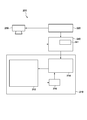
- FIG. 1 is a diagram showing a configuration example of a radiation imaging system 200 using the radiation imaging device 210 according to the embodiment of the present invention.
- the radiation imaging system 200 is configured to electrically image an optical image converted from radiation and obtain an electrical signal (radiation image data) for generating a radiation image.
- the radiation imaging system 200 includes, for example, a radiation imaging device 210, a radiation source 230, an irradiation control unit 220, and a computer 240.
- the radiation source 230 starts emitting radiation in accordance with an exposure command (radiation command) from the irradiation control unit 220.
- the radiation emitted from the radiation source 230 is applied to the radiation imaging device 210 through a subject (not shown).
- the radiation source 230 also stops the radiation of radiation in accordance with a stop command from the irradiation control unit 220.
- the radiation imaging device 210 includes an imaging panel 212 and a control unit 214 that controls the imaging panel 212.
- the control unit 214 generates a stop signal for stopping the radiation from the radiation source 230 based on the signal obtained from the image pickup panel 212.
- the stop signal is supplied to the irradiation control unit 220, and the irradiation control unit 220 sends a stop command to the radiation source 230 in response to the stop signal.
- the control unit 214 is, for example, a PLD (abbreviation for Programmable Logic Device) such as FPGA (abbreviation for Field Programmable Gate Array), or an ASIC (Application Specific Integrated Circuit) general-purpose program, abbreviated as a computer. It may consist of a computer or a combination of all or part of these.
- the computer 240 controls the radiation imaging device 210 and the irradiation control unit 220.
- the computer 240 includes a signal processing unit 241 that receives the radiation image data output from the radiation imaging device 210 and processes the radiation image data.
- the signal processing unit 241 can generate a radiographic image from the radiographic image data.
- the irradiation control unit 220 has an exposure switch (not shown) as an example, and when the exposure switch is turned on by the user, the irradiation command is sent to the radiation source 230 and a start notification indicating the start of radiation is started.
- the computer 240 Upon receiving the start notification, the computer 240 notifies the control unit 214 of the radiation imaging apparatus 210 of the start of radiation emission in response to the start notification.
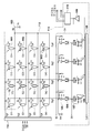
- FIG. 2 shows a configuration example of the imaging panel 212.
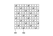
- the imaging panel 212 includes a pixel array 112.
- the pixel array 112 includes a plurality of pixel PIXs including conversion elements S (photoelectric conversion elements) arranged in a two-dimensional array for detecting radiation. Further, the pixel array 112 has a plurality of row signal lines Sigma1 to Sigma4 along the row direction (vertical direction in FIG. 2) for outputting the signal generated by the conversion element S.
- the image pickup panel 212 includes a drive circuit (row selection circuit) 114 for driving the pixel array 112, and a read circuit 113 for detecting a signal appearing in the column signal line Sigma of the pixel array 112. In the configuration shown in FIG.
- the pixel array 112 is composed of 4 rows ⁇ 4 columns of pixel PIX for simplification of description, but in reality, more pixel PIX may be arranged.
- the imaging panel 212 may have a size of 17 inches and a pixel PIX of about 3000 rows x about 3000 columns.
- Each pixel PIX has a conversion element S for detecting radiation, and a switch T for connecting the conversion element S and a column signal line SIG (a signal line Sigma corresponding to the conversion element C among a plurality of signal line sigs). including.
- Each conversion element S outputs a signal corresponding to the amount of incident radiation to the column signal line Sigma.
- the conversion element S may be, for example, a MIS type photodiode which is arranged on an insulating substrate such as a glass substrate and whose main material is amorphous silicon. Further, the conversion element S may be a PIN type photodiode.
- the conversion element S can be configured as an indirect element that detects light after converting radiation into light with a scintillator. In an indirect device, the scintillator can be shared by a plurality of pixel PIXs (plurality of conversion elements S).
- the switch T can be composed of, for example, a transistor such as a thin film transistor (TFT) having a control terminal (gate) and two main terminals (source and drain).
- the conversion element S has two main electrodes, one main electrode of the conversion element S is connected to one of the two main terminals of the switch T, and the other main electrode of the conversion element S is common. It is connected to the bias power supply 103 via the bias wire Bs.
- the bias power supply 103 supplies the bias voltage Vs.
- the control terminal of the switch T of each pixel PIX arranged in the first row is connected to the gate line Vg1 arranged along the row direction (horizontal direction in FIG. 2).
- control terminals of the switch SWs of the respective pixel PIX arranged in the second to fourth rows are connected to the gate lines Vg2 to Vg4, respectively.
- a gate signal is supplied to the gate lines Vg1 to Vg4 by the drive circuit 114.
- the main terminal on the side not connected to the conversion element S of the switch T is connected to the row signal line Sigma1 in the first row.
- the main terminals on the side not connected to the conversion element S of the switch T are connected to the row signal lines Sig2 to Sig4 in the second to fourth rows, respectively. ..
- the read circuit 113 has a plurality of column amplification units CA so that one column amplification unit CA corresponds to one column signal line Sigma.
- Each column amplification unit CA may include an integrating amplifier 105, a variable amplifier 104, a sample hold circuit 107, and a buffer circuit 106.
- the integrator amplifier 105 amplifies the signal appearing on the column signal line Sigma.
- the integrator amplifier 105 may include an operational amplifier and an integral capacitance and reset switch connected in parallel between the inverting input and output terminals of the operational amplifier.
- a reference potential Vref is supplied to the non-inverting input terminal of the operational amplifier.
- the reset switch can be controlled by the reset pulse RC supplied from the control unit 214.
- the variable amplifier 104 amplifies the signal output from the integrating amplifier 105 at a set amplification factor.
- the sample hold circuit 107 sample holds the signal output from the variable amplifier 104.
- the sample hold circuit 107 may be composed of a sampling switch and a sampling capacitance.
- the buffer circuit 106 buffers (impedance conversion) the signal output from the sample hold circuit 107 and outputs the signal.
- the sampling switch can be controlled by a sampling pulse supplied from the control unit 214.
- the read circuit 113 includes a multiplexer 108 that selects and outputs signals from a plurality of column amplification units CA provided so as to correspond to each column signal line Sigma in a predetermined order.
- the multiplexer 108 includes, for example, a shift register.
- the shift register performs a shift operation according to the clock signal CLK supplied from the control unit 214, and the shift register selects one signal from the plurality of column amplification units CA.
- the read circuit 113 further includes a buffer 109 that buffers (impedance conversion) the signal output from the multiplexer 108, and an AD converter 110 that converts an analog signal that is a signal output from the buffer 109 into a digital signal. sell.
- the output of the AD converter 110 that is, the radiographic image data, is transferred to the computer 240.
- scintillators that convert radiation into visible light are provided on both the incident surface side for incident radiation on the substrate and the back surface on the side opposite to the incident surface. It is arranged so as to cover the surface of.
- the conversion element S included in each pixel PIX includes two types of conversion elements S. In the configuration shown in FIG. 2, the conversion elements S12, S14, S21, S23, S32, S34, S41, and S43 are arranged so as to receive light from the two scintillators. In the following, when these conversion elements that receive light from two scintillators of the conversion elements S are specified, they are referred to as conversion elements 901.
- a light shielding layer 903 is arranged between one scintillator and each of the conversion elements S.
- the conversion elements S11, S13, S22, S24, S31, S33, S42, and S44 are arranged so that the light from one scintillator is blocked or dimmed and the light from the other scintillator is received.
- the light-shielding layer 903 is a layer that blocks the light emitted by the scintillator, and may shield light from either one of the scintillators covering the incident surface side or the back surface side of the substrate and the conversion element 902. At this time, the conversion element 902 does not have to completely block the light from one of the scintillators.
- a light-shielding layer 903 is provided between the conversion element 902 and either one of the scintillators covering the incident surface side or the back surface side of the substrate so that the amount of light received from one scintillator is smaller than that of the conversion element 901. It should be arranged.
- the light-shielding layer 903 is arranged between the scintillator arranged on the incident surface side of the substrate and the conversion element 902.
- the low-energy component is absorbed by the scintillator covering the incident surface side of the substrate, converted into visible light, and incident on each pixel PIX.
- the conversion element 902 has a light-shielding layer 903 arranged between the scintillator arranged on the incident surface side of the substrate and the conversion element 902, the light emitted by the scintillator on the incident surface side of the substrate is not incident. Therefore, the light converted from the low energy component of the radiation does not enter the conversion element 902.
- the conversion element 901 is not provided with the light shielding layer 903, the light converted from the component having low energy of radiation is incident.
- the high-energy component that was not absorbed by the scintillator arranged on the incident surface side of the substrate is absorbed by the scintillator that covers the back surface side of the substrate and converted into visible light.
- the back surface side of the substrate is not shielded from light, so that the light converted from the high-energy component of the radiation is incident on both the conversion element 901 and the conversion element 902.
- the conversion element S can efficiently receive light emitted from the scintillators arranged on the incident surface and the back surface with a simple element structure.
- the conversion element 901 can acquire the signal caused by the high energy component and the low energy component of the radiation, and the conversion element 902 can obtain the signal caused by the high energy component of the radiation. That is, information on different radiation energies can be held by pixel PIXs adjacent to each other. By holding the information acquired from the radiations of different energy components in the adjacent pixel PIXs in this way, energy subtraction can be performed by using the method described later.
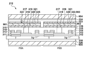
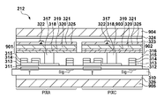
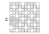
- 3A and 3B schematically show an example of a cross-sectional structure of a pixel PIXA having a conversion element 901 and a pixel PIXB and a pixel PIXC having a conversion element 902 arranged on the image pickup panel 212.
- the radiation is incident from the upper side of the drawing, but the radiation may be incident from the lower side of the drawing.
- the scintillator located on the side where the radiation is incident emits light mainly due to the low energy component of the radiation, and the scintillator placed on the other side mainly emits the high energy component of the radiation. It will emit the resulting light.
- FIG. 3A shows a case where the light-shielding layer 903 is arranged between the conversion element 902 and the scintillator 904 in the pixel PIXB.
- FIG. 3B is the same as in FIG. 3A in that the conversion element 901 and the conversion element 902 are arranged between the substrate 310 and the scintillator 904 that covers the incident surface side of the substrate 310.
- the light-shielding layer 903 is arranged between the conversion element 902 and the scintillator 905 arranged on the back surface side opposite to the incident surface of the substrate 310.
- the conversion element S of each pixel PIX is arranged on a substrate 310 having an insulating property such as a glass substrate that transmits the light emitted by the scintillators 904 and 905.
- the pixel PIX is arranged on the conductive layer 311 arranged on the substrate 310, the insulating layer 312 arranged on the conductive layer 311 and the semiconductor layer 313 and the semiconductor layer 313 arranged on the insulating layer 312. Includes the impurity semiconductor layer 314 and the conductive layer 315 arranged on the impurity semiconductor layer 314.
- the conductive layer 311 constitutes a gate electrode of a transistor (for example, a TFT) constituting the switch T.
- the insulating layer 312 is arranged so as to cover the conductive layer 311, and the semiconductor layer 313 is arranged on the portion of the conductive layer 311 constituting the gate electrode via the insulating layer 312.
- the impurity semiconductor layer 314 is arranged on the semiconductor layer 313 so as to form two main terminals (source and drain) of the transistor constituting the switch T.
- the conductive layer 315 constitutes a wiring pattern connected to each of the two main terminals (source and drain) of the transistors constituting the switch T.
- a part of the conductive layer 315 constitutes the column signal line Sigma, and the other part constitutes a wiring pattern for connecting the conversion element S and the switch T.
- Each pixel PIX further includes an interlayer insulating film 316 that covers the insulating layer 312 and the conductive layer 315.
- the interlayer insulating film 316 is provided with a contact plug 317 for connecting to a portion of the conductive layer 315 that constitutes the switch T.
- each pixel PIX includes a conversion element S arranged on the interlayer insulating film 316.
- the conversion element S is configured as an indirect photoelectric conversion element that converts light converted from radiation by scintillators 904 and 905 into an electric signal.
- the conversion element S includes a conductive layer 318, an insulating layer 319, a semiconductor layer 320, an impurity semiconductor layer 321 and a conductive layer 322, and an electrode layer 325 laminated on the interlayer insulating film 316.
- a protective layer 323 and an adhesive layer 324 are arranged on the conversion element S.
- the scintillator 904 is arranged on the adhesive layer 324 so as to cover the incident surface side of the substrate 310. Further, the scintillator 905 is arranged so as to cover the back surface side of the substrate 310 opposite to the incident surface.
- Each of the conductive layers 318 constitutes a lower electrode of the conversion element S. Further, the conductive layer 322 and the electrode layer 325 form the upper electrodes of the respective conversion elements S.
- the conductive layer 318, the insulating layer 319, the semiconductor layer 320, the impurity semiconductor layer 321 and the conductive layer 322 form a MIS type sensor as the conversion element S.
- the impurity semiconductor layer 321 is formed of an n-type impurity semiconductor layer.
- the scintillators 904 and 905 can be constructed by using a material such as GOS (gadolinium sulfide) or CsI (cesium iodide). These materials can be formed by laminating, printing, vapor deposition, etc.
- the scintillator 904 and the scintillator 905 may use the same material, or different materials may be used depending on the energy of the radiation to be acquired.
- the conversion element S shows an example of using a MIS type sensor, but the conversion element S is not limited to this.
- the conversion element S may be, for example, a pn type or PIN type photodiode.
- the conversion element 902 represented by the pixel PIXB includes a semiconductor layer 320, a conductive layer 318 forming a lower electrode arranged on the incident surface side of the substrate 310 of the semiconductor layer 320, and a semiconductor layer 320.
- a conductive layer 322 that constitutes an upper electrode arranged on the side of the scintillator 904.
- the conductive layer 322 constituting the upper electrode functions as a light-shielding layer 903.
- the conductive layer 322 functions as a light-shielding layer 903 by forming the conductive layer 322 with a material such as Al, Mo, Cr, or Cu that is opaque to the light emitted by the scintillator 904. That is, the light-shielding layer 903 is arranged between the scintillator 904 and the conversion element 902 so that the conversion element 902 of the pixel PIXB can receive less light from the scintillator 904 than the conversion element 901. Further, the conversion element 902 of the pixel PIXB is arranged so as to receive the light from the scintillator 905, similarly to the conversion element 901 represented by the pixel PIXA. Further, in the configuration shown in FIG.
- the conversion element 902 represented by the pixel PIXC includes a semiconductor layer 320, a conductive layer 318 constituting a lower electrode arranged on the incident surface side of the substrate 310 of the semiconductor layer 320, and a semiconductor. It includes a conductive layer 322 that constitutes an upper electrode arranged on the side of the scintillator 904 of the layer 320.
- the conductive layer 318 constituting the lower electrode functions as a light-shielding layer 903. Specifically, by forming the conductive layer 318 with a material such as Al, Mo, Cr, Cu, which is opaque to the light emitted by the scintillator 905, the conductive layer 322 functions as the light-shielding layer 903.
- the light-shielding layer 903 is arranged between the scintillator 905 and the conversion element 902 so that the conversion element 902 of the pixel PIXC can receive less light from the scintillator 905 than the conversion element 901. Further, the conversion element 902 of the pixel PIXC is arranged so as to receive the light from the scintillator 904, similarly to the conversion element 901 of the pixel PIXA.
- the conversion element 901 of the pixel PIXA a material transparent to the light emitted by the scintillator 904, such as ITO (indium tin oxide), is used for the conductive layer 318 and the electrode layer 325.
- ITO indium tin oxide
- the plurality of conversion elements S include the plurality of conversion elements 901 and the plurality of conversion elements 902 having different sensitivities for detecting the light emitted by at least one of the scintillator 904 and the scintillator 905.
- the present invention is not limited to this.
- a transparent material and an opaque material may be laminated, in which case the amount of light shielding is determined by the area of the opaque material.
- the conductive layer 322 of the pixel PIXB and the conductive layer 318 of the pixel PIXC are made to function as the light-shielding layer 903, but the arrangement of the light-shielding layer 903 is not limited to this.
- a dedicated light-shielding layer 903 using Al, Mo, Cr, Cu, or the like may be arranged in the protective layer 323 with respect to the light incident from the scintillator 904.
- the potential of the light-shielding layer 903 may be fixed at a constant potential.
- the positions of the switch T and the column signal line Sigma of the pixel PIXA that receives the light from the scintillator 905 are moved toward the pixel PIXC. You may arrange it. With such an arrangement, the aperture ratio of the conversion element 901 with respect to the scintillator 905 can be increased in the pixel PIXA.
- the light-shielding layer 903 does not need to completely block the light from the scintillator 904 or the scintillator 905 to the conversion element 902 as described above. Energy subtraction is possible if the amount of light received from the scintillator 904 or the scintillator 905 on the side where the light-shielding layer 903 is arranged differs between the adjacent pixel PIXA and the pixel PIXB or the pixel PIXC. In such a case, it is investigated in advance what percentage of the light received by the conversion element 901 of the pixel PIXA is incident on the conversion element 902 of the pixel PIXB or the pixel PIXC, and the output of the conversion element 901 is output. It can be corrected by performing difference processing on the reference.
- each of the column signal lines Sigma is arranged so as to overlap a part of the pixel PIX in the normal projection on the incident surface of the substrate 310.
- Such a configuration is advantageous in that the area of the conversion element S of each pixel PIX is increased, but is disadvantageous in that the capacitive coupling between the column signal line Sigma and the conversion element S is large. is there.
- the column signal line Sigma is capacitively coupled between the column signal line Sigma and the conversion element S. Cross talk occurs in which the potential of the is changed. 4A-4D show how to deal with this crosstalk.
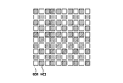
- the number of pixel PIXs having the conversion elements 902 to which the included light-shielding layer 903 is arranged is arranged to be the same for each row. To do. Further, in the conversion elements S arranged in the column direction among the plurality of conversion elements S, the number of pixels PIX having the plurality of conversion elements 902 included is the same for each row. By arranging in this way, it is possible to suppress the occurrence of artifacts due to crosstalk in units of rows and columns.
- the radiation imaging device 210 may have a function of automatically detecting the start of radiation irradiation.
- the gate wire Vg is operated so that the switch T is turned on / off, the signal from the conversion element S is read out, and the presence or absence of radiation irradiation is determined from the output signal.
- the number of pixels PIX having the conversion element 902 including the light-shielding layer 903 is different for each row, the amount of signals output for each row changes, and the detection accuracy varies. Therefore, as shown in FIGS.
- the number of pixel PIXs having the conversion elements 902 on which the light shielding layer 903 is arranged is large. , Arrange so that it is the same for each line. With such an arrangement, the detection accuracy of automatically detecting the start of radiation irradiation is stabilized.
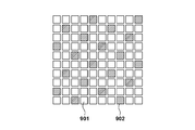
- the arrangement example of the pixel PIX in FIGS. 4B and 4D reduces the density of the pixel PIX having the conversion element 902 as compared with the arrangement example of the pixel PIX in FIGS. 4A and 4C. Since the light from the scintillator 905 is incident on the conversion element S via the substrate 310, the light is diffused depending on the thickness of the substrate 310, and the MTF (Modulation Transfer Function) is lowered. Therefore, even if the density of the pixel PIX having the conversion element 902 is reduced, the resolving power does not substantially decrease.
- MTF Modulation Transfer Function
- the number of pixel PIXs including the conversion element 902 is larger than the number of pixel PIXs including the conversion element 901. May be less.
- the operation of the radiation imaging device 210 is controlled by, for example, the computer 240.
- the operation of the radiation imaging device 210 is controlled by the control unit 214 under the control of the computer 240.
- the control unit 214 under the control of the computer 240.
- the light-shielding layer 903 is arranged between the conversion element 902 and the scintillator 904 as in the configuration shown in FIG. 3A.
- a gate signal Von is supplied to the gate lines Vg1 to Vg4 so that the switches T are sequentially turned on, and a reset operation is performed in which each conversion element S is reset.
- the start of radiation irradiation can be detected by the detection circuit 216 that detects the current flowing through the bias line Bs, the column signal line Sig, and the like.
- the radiation irradiation start may be detected by a signal supplied from the computer 240 to the radiation imaging device 210 without being limited to this.
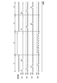
- the radiation imaging apparatus 210 transitions from the period T1 to the period T2.
- the period T2 is the period during which the radiation is irradiated.
- the period T2 is a period from the detection of the start of radiation irradiation to the time when the irradiation amount of radiation becomes an appropriate dose for acquiring radiation image data. Therefore, it can be said that the period T2 is a period for monitoring the irradiation amount of radiation. That is, in this embodiment, it can be said that the radiation imaging device 210 has an automatic exposure control (AEC) function.
- AEC automatic exposure control
- the gate signal Von is applied to the gate line Vg4 so that the switches T41 to T44 are turned on, respectively, and the signals accumulated in the conversion elements S41 to S44 are sequentially read out. Further, a gate signal Voff is supplied to the gate lines Vg1 to Vg3 so that the switches T11 to T14, T21 to T24, and T31 to T34 are turned off. Therefore, charges based on the light converted by the scintillators 904 and 905 from the incident radiation are accumulated in the conversion elements S11 to S14, S21 to S24, and S31 to S34.
- the component having high radiation energy passes through the subject (not shown) and the scintillator 904, is absorbed by the scintillator 905 and converted into light, the dose of radiation incident on the scintillator 905 is attenuated. It ends up. For this reason, the signal value of the signal corresponding to the light converted by the scintillator 905 becomes small, and for example, noise such as an offset signal of the conversion element S or the switch T, or such noise varies in the plane. There is a possibility that the signal will be buried in such as. As a result, the accuracy of acquiring signals of high-energy components of radiation may be reduced, and the image quality of the generated energy subtraction image may be reduced.
- the control unit 214 acquires a signal corresponding to the light converted from the radiation by the scintillator 905, in other words, a signal corresponding to the high energy component of the radiation during the irradiation of the radiation. That is, the control unit 214 outputs the signals output from the conversion elements S42 and S44 used as the measurement elements selected from the conversion elements 902 that receive the light converted by the scintillator 905 during the period T2 when the radiation is irradiated. get. Based on the signal corresponding to the light converted from the radiation by the scintillator 905, the control unit 214 outputs a signal for stopping the irradiation of the radiation to the radiation imaging device 210.
- control unit 214 determines whether or not the cumulative value of the signal corresponding to the light converted from the radiation by the scintillator 905 has reached a preset set value.
- the control unit 214 outputs a stop signal for stopping the irradiation of the radiation to the irradiation control unit 220 when the cumulative value of the signals corresponding to the light converted from the radiation by the scintillator 905 reaches the set value.
- the control unit 214 may transmit a stop signal to the irradiation control unit 220 via the computer 240, or may transmit the stop signal directly to the irradiation control unit 220 or the radiation source 230.
- This set value is set in advance based on, for example, the noise level of the pixel PIX such as the conversion element S or the switch T when no radiation is applied (here, simply referred to as “noise level of the conversion element S”). sell.
- this set value may be a value five times or more the signal value corresponding to the noise level of the conversion element S (SNR is 5 or more).
- the set value may be a value 10 times or more the signal value corresponding to the noise level of the conversion element S (SNR is 10 or more).
- the set value may be a value 20 times or more the signal value corresponding to the noise level of the conversion element S (SNR is 20 or more).
- the signal due to the light converted from the radiation by the scintillator 904 in other words, the signal due to the low energy radiation (the signal output from the conversion elements S41 and S43 used as the measurement element) is also It may be monitored in the same way.
- the light-corresponding signal converted by the scintillator 904 may reach the conversion element S in a larger amount than the light-corresponding signal converted by the scintillator 905. Therefore, the signal (charge) corresponding to the light converted by the scintillator 904 is saturated before the cumulative value of the signals acquired according to the light converted by the scintillator 905 reaches the above-mentioned set value. there is a possibility.
- the conversion element 901 including the conversion elements S41 and S43 receives both the lights converted by the scintillators 904 and 905, so that the possibility of becoming more saturated may increase. Therefore, the control unit 214 also acquires the cumulative value of the signals corresponding to the light from the scintillators 904 and 905, and sets in advance based on the saturation level of the conversion elements S41 and S43 selected from the conversion element 901 as the measurement element. It is determined whether or not the set value has been reached.
- control unit 214 acquires not only the signal corresponding to the light converted by the scintillator 905 but also the signal corresponding to the light converted by the scintillator 904, and stops the irradiation of radiation based on these signals.
- the stop signal of may be output.
- the control unit 214 may be provided with a plurality of set values according to the imaging conditions in advance, for example, in the memory in the control unit 214. ..
- the respective set values may be set to an intermediate value between the signal value of the saturation level estimated from the signal of the conversion element 901 and the signal value of the noise level estimated from the signal of the conversion element 902.
- the radiation imaging device 210 controls the irradiation of radiation based on the signal corresponding to the light converted by the scintillator 905 caused by the high-energy radiation. This makes it possible to improve the accuracy of signals caused by high-energy radiation. Further, the signal corresponding to the light converted by the scintillator 904 caused by the low energy radiation is also measured. As a result, the conversion element 901 is saturated, and unnecessary exposure to the patient or the like, such as re-shooting, can be suppressed. As a result, it is possible to obtain a radiation imaging device 210 with improved accuracy of the obtained energy subtraction image.
- the period T3 is a period for reading out the signals accumulated in the conversion elements S11 to S14, S21 to S24, and S31 to S34 according to the light converted from the radiation after the irradiation of the radiation is completed.
- a gate signal Von that sequentially turns on the switches T11 to T14, T21 to T24, and T31 to T34 is supplied to the gate lines Vg1 to Vg3, and reading is performed.
- the gate signal Voff is supplied to the gate line Vg4 so that the switches T41 to T44 are turned off.
- Period T4 is the offset data acquisition period.
- the conversion element S continues to accumulate dark charges even when it is not irradiated with radiation. Therefore, the control unit 214 acquires the offset image data by performing the same operation as when acquiring the radiation image data without irradiating the radiation. By subtracting the offset image data from the radiation image data, the offset component due to the dark charge can be removed.
- the periods T3 and T4 may be a period in which the control unit 214 causes the conversion element 901 and the conversion element 902 to output a signal for generating an energy subtraction image after irradiation with radiation.
- the signals output from the conversion element 901 and the conversion element 902 are transmitted to, for example, the signal processing unit 241 of the computer 240.
- the signal processing unit 241 generates an energy subtraction image based on the signal output from each of the conversion elements 901 and the signal output from each of the conversion elements 902, and a display (not shown) connected to the computer 240 or the like is generated. Display on. This allows the user to observe a radiographic image (subtraction image).
- the conversion element 902 receives radiation from the upper part of the figure, shields the light from the scintillator 905, and receives light caused by low-energy radiation from the scintillator 904. It is explained as. Further, in the following, the radiation image data output from the conversion element 901 may be referred to as double-sided image data, and the radiation image data output from the conversion element 902 may be referred to as single-sided image data.
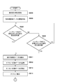
- control unit 214 when the control unit 214 detects the start of radiation irradiation as described above, it transitions to S930.
- the control unit 214 is a measuring element (for example, S41 to 44 described above) selected for measuring the dose of incident radiation among the conversion elements S in order to obtain a radiation image (energy subtraction image). Starts getting the signal from. Further, the conversion element S other than the measurement element starts a storage operation of accumulating charges according to the light converted from the incident radiation in order to acquire the radiation image data.
- the control unit 214 acquires a signal corresponding to the light converted from the radiation by the scintillator 905 in which the radiation transmitted through the scintillator 904 is incident, and determines whether to continue or stop the irradiation of the radiation based on this signal (S950). ).
- the conversion element 901 outputs a signal corresponding to the light converted by the scintillator 904 and the scintillator 905, and the conversion element 902 outputs a signal corresponding to the light converted by the scintillator 904. ..
- control unit 214 has a signal output from the measurement element (for example, conversion elements S41 and S43) selected from the conversion element 901 and a signal output from the conversion element 902 (for example, conversion elements S42 and S44). Based on the difference between and, the signal corresponding to the light converted by the scintillator 905 is acquired.
- the measurement element for example, conversion elements S41 and S43
- a signal output from the conversion element 902 for example, conversion elements S42 and S44
- the control unit 214 acquires not only the scintillator 905 but also a signal corresponding to the light converted from the radiation by the scintillator 904, and determines the continuation or stop of the radiation irradiation based on this signal. It may be (S940).
- the conversion element 901 outputs a signal corresponding to the light converted by the scintillator 904 and the scintillator 905, and the conversion element 902 outputs a signal corresponding to the light converted by the scintillator 904.
- the control unit 214 includes a signal output from the measurement element (for example, conversion elements S41 and S43) selected from the conversion element 901 and a signal output from the conversion element 902 (for example, conversion elements S42 and S44).
- the determination of S940 may be made using both of the above. Further, the control unit 214 may determine S940 using only the signals output from the measurement elements (for example, conversion elements S41 and S43) selected from the conversion element 901.
- the determination of S950 and the determination of S940 are alternately performed in S950 or S940 until it is determined that any of the respective signal values reaches the corresponding set value, as shown in FIG. 6A. It may be good (NO of S950 and S940). Further, when the determination of S950 and the determination of S940 are performed, the determination of S940 with high sensitivity is made in consideration of the case where radiation having a very large dose is irradiated due to a setting error or the like, as shown in FIG. 6A. , It may be performed first after the start of irradiation.
- control unit 214 determines that any of the respective signal values reaches the corresponding set value (YES in S950 and S940)
- the control unit 214 stops to stop the irradiation of radiation.
- control unit 214 outputs the signal generated by the conversion element S via the drive circuit 114 and the read circuit 113, and reads out the radiographic image data.
- the radiographic image data is output to the computer 240.
- the control unit 214 performs an accumulation operation for acquiring the offset image data in S912, causes the drive circuit 114 and the read circuit 113 to read the offset image data in S913, and outputs the offset image data to the computer 240.
- the signal processing unit 241 of the computer 240 performs offset correction by subtracting the radiation image data acquired in S911 with the offset image data acquired in S913.
- the signal processing unit 241 separates the radiation image data after offset correction into the radiation image data output from the conversion element 901 and the radiation image data output from the conversion element 902.
- the signal processing unit 241 performs gain correction of the double-sided image data using the gain correction image data taken in the absence of the subject. Further, the signal processing unit 241 performs gain correction of the single-sided image data in S917 by using the gain correction image data.
- the signal processing unit 241 After performing the gain correction, the signal processing unit 241 performs pixel interpolation in S918 to compensate for the lack of double-sided image data of the pixel PIX that does not include the conversion element 901, in other words, the pixel PIX that has the conversion element 902. Similarly, in S919, the signal processing unit 241 performs pixel interpolation for compensating for the lack of single-sided image data of the pixel PIX that does not include the conversion element 902, in other words, the pixel PIX that has the conversion element 901.
- the pixel interpolation in S918 and S919 will be described with reference to FIGS. 7A and 7B.
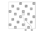
- FIG. 4D an arrangement in which the number of pixel PIXs including the conversion element 901 is larger than the number of pixel PIXs including the conversion element 902 will be described as an example.
- the double-sided image data of the pixel E having the conversion element 902 for outputting the single-sided image data is the pixels A, B, C, D, F, G, H having the conversion element 901 for outputting the double-sided image data adjacent to the pixel E.
- the signal processing unit 241 may interpolate the double-sided image data of the pixel E by using the average value of the double-sided image data of eight pixels adjacent to the pixel E.
- the signal processing unit 241 may interpolate the double-sided image data of the pixel E by using the average value of the double-sided image data of some adjacent pixels, such as the pixels B, D, F, and H. .. In S918, by performing pixel interpolation, radiation image data generated by the high energy component and the low energy component of the radiation of each pixel PIX is generated.
- the signal processing unit 241 may interpolate the single-sided image data of the pixel J by using the average value of the single-sided image data of four pixels adjacent to the pixel J. In this case, for example, the distance from the position where the pixel J is arranged to the pixel K and the distance to the pixel N are different.
- the single-sided image data output from the pixels K, L, M, and N may be weighted and averaged according to the distance.
- S919 by performing pixel interpolation, radiation image data generated by the low energy component of the radiation of each pixel PIX is generated.
- the signal processing unit 241 generates radiation image data based on the high energy component of radiation in S920.
- the single-sided image data becomes radiation image data with a low energy component.
- the double-sided image data is radiation image data having both high-energy and low-energy components. Therefore, it is possible to generate high-energy component radiographic image data by subtracting the pixel-stored single-sided image data from the pixel-interpolated double-sided image data.
- the single-sided image data becomes the radiation image data due to the high energy component. Therefore, it is possible to generate low-energy component radiation image data by subtracting the pixel-stored single-sided image data from the pixel-interpolated double-sided image data.
- the radiation image with the high energy component is the component of the radiation that could not be completely absorbed by the scintillator 904 on the side where the radiation is incident, the amount of light from the scintillator 905 is larger than the amount of light from the scintillator 904. Few. Therefore, when the single-sided image data is subtracted from the double-sided image data to generate the high-energy component radiation image data, the noise of the low-energy component radiation image data is added to the high-energy component radiation image data. As a result, the S / N ratio of the radiographic image data of the high energy component becomes low.
- the side where the radiation of the conversion element 902 is incident is shielded from light, and the double-sided image data is set to the high energy component + low energy component, and the single-sided image data is set to the high energy component image data. Then, the S / N ratio can be improved by subtracting the single-sided image data from the double-sided image data to generate a low-energy image.
- the signal processing unit 241 generates an energy subtraction image in S922. Specifically, the signal processing unit 241 calculates the difference between the signal output from the conversion element 901 acquired in S920 and the signal output from the conversion element 902 and the difference between the signal output from the conversion element 902. Take. As a result, an energy subtraction image which is a difference between the radiation image data of the high energy component and the radiation image data of the low energy component is generated.
- the signal processing unit 241 may generate a normal radiation image without energy subtraction in S920 based on the double-sided image data output from the conversion element 901 in S918.
- the conversion element 901 receives the light from the scintillator 904 on the side where the radiation is incident and the light from the scintillator 905 on the side opposite to the side where the radiation is incident.
- a higher S / N ratio can be obtained in a normal radiographic image than in the case of receiving only the light emitted by one scintillator.
- a light-shielding layer for blocking light from the scintillator 904 or the scintillator 905 only in a part of the pixel PIXs including the conversion element 902 among the plurality of pixel PIXs. 903 is arranged. That is, since it is only necessary to add the light-shielding layer 903 to a part of the pixel PIX, it is possible to realize a radiation imaging device capable of acquiring an energy subtraction image while suppressing the manufacturing cost without complicating the structure.
- the conversion element 901 receives the light emitted from the scintillator 904 and the scintillator 905, the sensitivity to the incident radiation is improved, and as a result, the image quality of the obtained radiation image can be improved. Further, even when generating a normal radiation image, a radiation image is generated from a signal generated by receiving the light emitted by the two scintillators 904 and 905. Therefore, as compared with the structure as in Patent Document 1, the S / N ratio when a normal radiographic image is taken is improved.
- one imaging panel 212 can be used to record a radiation image of radiation of two different energy components with one irradiation (one-shot method) on the subject. Therefore, as compared with the radiation imaging device that generates an energy subtraction image using two imaging panels, the number of parts of the radiation imaging device is reduced, and the manufacturing cost can be reduced. Further, since the weight of the radiation imaging device 210 can be reduced, it is possible to realize a radiation imaging device that is convenient for a portable user. Further, since the energy subtraction image is generated by one imaging panel, it is possible to realize a radiation imaging apparatus that does not cause a problem of positional deviation between the photoelectric conversion elements between the two imaging panels. Further, it is possible to realize a radiation imaging device capable of generating a radiation image having a high S / N ratio in generating a normal radiation image as well as an energy subtraction image.
- control unit 214 measures the signal caused by the scintillator 905, which reduces the amount of light converted from the radiation, during the irradiation of the radiation.
- the signal corresponding to the light converted by the scintillator 905 can be acquired without being buried in noise.
- image quality of the obtained subtraction image is improved, and it is possible to improve the accuracy of image diagnosis by a doctor, for example.
- the scintillators 904 and 9050 are arranged so as to cover both sides of one substrate 310 as the imaging panel 212 of the radiation imaging apparatus 210, but the present invention is not limited to this.
- the two imaging panels P1 and P2 may be applied as the imaging panel 212 of the radiation imaging apparatus 210.
- the two imaging panels P1 and P2 may be panels having the same structure as each other.
- each pixel PIX does not have to include the light-shielding layer 903 as described above. That is, in the configuration shown in FIG. 8, each conversion element S may have the same configuration as the conversion element 901 shown in FIGS. 3A and 3B. Further, in the configuration shown in FIG.
- the scintillator arranged on the image pickup panel P1 arranged on the side where the radiation is incident corresponds to the scintillator 904 described above
- the scintillator arranged on the other image pickup panel P2 is It corresponds to the scintillator 905 described above.
- the control unit 214 acquires a signal corresponding to the light converted from the radiation by the scintillator 905, and based on this signal, stops the irradiation of the radiation imaging device 210 with radiation. Is judged. That is, if the control unit 214 acquires the signal output from the conversion element 9012 arranged on the image pickup panel P2 and determines whether to continue or stop the irradiation of radiation based on the signal output from the conversion element 9012. Good.
- the substrate 310 of the image pickup panel P1 may be opaque to the light generated by the scintillator 904 so that the light converted by the scintillator 904 of the image pickup panel P1 does not enter the conversion element 9012. ..
- the image pickup panel P1 and the image pickup panel P2 may be each covered with a light-shielding film or the like. Further, as described above, the signal output from the conversion element 9011 arranged on the image pickup panel P1 may also be used in parallel to determine whether to continue or stop the radiation irradiation.
- the signal corresponding to the light converted by the scintillator 905 due to the high energy component of the radiation can be acquired without being buried in noise. As a result, it is possible to improve the image quality of the obtained energy subtraction image.
Landscapes
- Health & Medical Sciences (AREA)
- Life Sciences & Earth Sciences (AREA)
- Physics & Mathematics (AREA)
- High Energy & Nuclear Physics (AREA)
- Molecular Biology (AREA)
- Spectroscopy & Molecular Physics (AREA)
- General Physics & Mathematics (AREA)
- Engineering & Computer Science (AREA)
- Multimedia (AREA)
- Signal Processing (AREA)
- Medical Informatics (AREA)
- Nuclear Medicine, Radiotherapy & Molecular Imaging (AREA)
- Surgery (AREA)
- Crystallography & Structural Chemistry (AREA)
- Chemical & Material Sciences (AREA)
- Optics & Photonics (AREA)
- Pathology (AREA)
- Radiology & Medical Imaging (AREA)
- Biomedical Technology (AREA)
- Heart & Thoracic Surgery (AREA)
- Biophysics (AREA)
- Animal Behavior & Ethology (AREA)
- General Health & Medical Sciences (AREA)
- Public Health (AREA)
- Veterinary Medicine (AREA)
- Measurement Of Radiation (AREA)
- Apparatus For Radiation Diagnosis (AREA)
- Solid State Image Pick-Up Elements (AREA)
- Transforming Light Signals Into Electric Signals (AREA)
- Light Receiving Elements (AREA)
Priority Applications (1)
| Application Number | Priority Date | Filing Date | Title |
|---|---|---|---|
| US17/525,441 US11693131B2 (en) | 2019-05-29 | 2021-11-12 | Radiation imaging apparatus and radiation imaging system |
Applications Claiming Priority (2)
| Application Number | Priority Date | Filing Date | Title |
|---|---|---|---|
| JP2019100723A JP7157699B2 (ja) | 2019-05-29 | 2019-05-29 | 放射線撮像装置、放射線撮像システム、放射線撮像装置の制御方法および当該方法を実行させるプログラム |
| JP2019-100723 | 2019-05-29 |
Related Child Applications (1)
| Application Number | Title | Priority Date | Filing Date |
|---|---|---|---|
| US17/525,441 Continuation US11693131B2 (en) | 2019-05-29 | 2021-11-12 | Radiation imaging apparatus and radiation imaging system |
Publications (1)
| Publication Number | Publication Date |
|---|---|
| WO2020241062A1 true WO2020241062A1 (ja) | 2020-12-03 |
Family
ID=73548662
Family Applications (1)
| Application Number | Title | Priority Date | Filing Date |
|---|---|---|---|
| PCT/JP2020/015692 Ceased WO2020241062A1 (ja) | 2019-05-29 | 2020-04-07 | 放射線撮像装置および放射線撮像システム |
Country Status (3)
| Country | Link |
|---|---|
| US (1) | US11693131B2 (https=) |
| JP (1) | JP7157699B2 (https=) |
| WO (1) | WO2020241062A1 (https=) |
Cited By (2)
| Publication number | Priority date | Publication date | Assignee | Title |
|---|---|---|---|---|
| EP4043929A1 (fr) * | 2021-02-11 | 2022-08-17 | Trixell | Detecteur numerique a etages de conversion superposes |
| WO2024154438A1 (ja) * | 2023-01-18 | 2024-07-25 | パナソニックIpマネジメント株式会社 | 撮像装置およびカメラシステム |
Families Citing this family (7)
| Publication number | Priority date | Publication date | Assignee | Title |
|---|---|---|---|---|
| JP7410678B2 (ja) | 2019-09-19 | 2024-01-10 | キヤノン株式会社 | 放射線撮像装置および放射線撮像システム |
| JP7737236B2 (ja) | 2021-04-16 | 2025-09-10 | キヤノン株式会社 | 放射線撮像装置および放射線撮像システム |
| JP2023111636A (ja) | 2022-01-31 | 2023-08-10 | キヤノン株式会社 | 放射線撮像装置および放射線撮像システム |
| US12339408B2 (en) | 2022-02-16 | 2025-06-24 | Canon Kabushiki Kaisha | Radiation imaging apparatus and radiation imaging system |
| JP2024075034A (ja) * | 2022-11-22 | 2024-06-03 | キヤノン株式会社 | 放射線撮像装置及び放射線撮像システム |
| JPWO2024161772A1 (https=) * | 2023-02-02 | 2024-08-08 | ||
| JPWO2024161771A1 (https=) * | 2023-02-02 | 2024-08-08 |
Citations (5)
| Publication number | Priority date | Publication date | Assignee | Title |
|---|---|---|---|---|
| WO2008120293A1 (ja) * | 2007-03-01 | 2008-10-09 | Shimadzu Corporation | X線撮影装置 |
| JP2011022132A (ja) * | 2009-06-17 | 2011-02-03 | Fujifilm Corp | 放射線検出装置及び放射線画像検出システム |
| JP2018023769A (ja) * | 2016-07-29 | 2018-02-15 | 富士フイルム株式会社 | 放射線画像撮影システム、放射線画像撮影方法、及び放射線画像撮影プログラム |
| JP2018186468A (ja) * | 2017-04-27 | 2018-11-22 | キヤノン株式会社 | 放射線撮像装置、放射線撮像システム、放射線撮像装置の制御方法及びプログラム |
| WO2019093168A1 (ja) * | 2017-11-10 | 2019-05-16 | キヤノン株式会社 | 放射線撮像装置および放射線撮像システム |
Family Cites Families (31)
| Publication number | Priority date | Publication date | Assignee | Title |
|---|---|---|---|---|
| JP2010056396A (ja) | 2008-08-29 | 2010-03-11 | Fujifilm Corp | X線検出素子 |
| JP5731444B2 (ja) * | 2011-07-07 | 2015-06-10 | 富士フイルム株式会社 | 放射線検出器、放射線画像撮影装置、及び放射線画像撮影システム |
| JP5954983B2 (ja) | 2011-12-21 | 2016-07-20 | キヤノン株式会社 | 撮像装置及び放射線撮像システム、並びに撮像装置の製造方法 |
| JP6057511B2 (ja) | 2011-12-21 | 2017-01-11 | キヤノン株式会社 | 撮像装置及び放射線撮像システム |
| JP2014003542A (ja) | 2012-06-20 | 2014-01-09 | Canon Inc | 検出装置、検出システム及び検出装置の駆動方法 |
| JP2014110352A (ja) | 2012-12-03 | 2014-06-12 | Canon Inc | 検出装置の製造方法 |
| JP6463136B2 (ja) | 2014-02-14 | 2019-01-30 | キヤノン株式会社 | 放射線検出装置及び放射線検出システム |
| JP6480670B2 (ja) | 2014-05-01 | 2019-03-13 | キヤノン株式会社 | 放射線撮像装置および放射線撮像システム |
| JP6339853B2 (ja) | 2014-05-01 | 2018-06-06 | キヤノン株式会社 | 放射線撮像装置および放射線撮像システム |
| JP6585910B2 (ja) | 2014-05-01 | 2019-10-02 | キヤノン株式会社 | 放射線撮像装置および放射線撮像システム |
| JP6442163B2 (ja) | 2014-06-02 | 2018-12-19 | キヤノン株式会社 | 放射線撮像装置および放射線撮像システム |
| JP6595803B2 (ja) | 2014-06-13 | 2019-10-23 | キヤノン株式会社 | 放射線撮像装置、放射線撮像システムおよびその制御方法 |
| US9948871B2 (en) | 2014-07-25 | 2018-04-17 | Canon Kabushiki Kaisha | Radiation imaging apparatus and radiation imaging system |
| JP6378573B2 (ja) | 2014-08-06 | 2018-08-22 | キヤノン株式会社 | 放射線撮像装置及び放射線撮像システム |
| JP6491434B2 (ja) | 2014-08-12 | 2019-03-27 | キヤノン株式会社 | 放射線撮像装置及び放射線検出システム |
| JP6555909B2 (ja) | 2015-03-20 | 2019-08-07 | キヤノン株式会社 | 放射線撮像装置及び放射線撮像システム |
| JP6570315B2 (ja) | 2015-05-22 | 2019-09-04 | キヤノン株式会社 | 放射線撮像装置及び放射線撮像システム |
| JP6626301B2 (ja) | 2015-09-28 | 2019-12-25 | キヤノン株式会社 | 放射線撮像装置、放射線撮像システム、放射線撮像装置の制御方法及びプログラム |
| JP6649775B2 (ja) | 2016-01-13 | 2020-02-19 | キヤノン株式会社 | 放射線撮像装置、その駆動方法及び放射線撮像システム |
| JP6695232B2 (ja) * | 2016-07-29 | 2020-05-20 | 富士フイルム株式会社 | 放射線画像撮影システム |
| JP6639353B2 (ja) * | 2016-07-29 | 2020-02-05 | 富士フイルム株式会社 | 放射線画像撮影システム、放射線画像撮影方法、及び放射線画像撮影プログラム |
| JP6929104B2 (ja) | 2017-04-05 | 2021-09-01 | キヤノン株式会社 | 放射線撮像装置、放射線撮像システム、放射線撮像装置の制御方法及びプログラム |
| JP6853729B2 (ja) | 2017-05-08 | 2021-03-31 | キヤノン株式会社 | 放射線撮像装置、放射線撮像システム、放射線撮像装置の制御方法及びプログラム |
| JP6788547B2 (ja) | 2017-05-09 | 2020-11-25 | キヤノン株式会社 | 放射線撮像装置、その制御方法、制御装置、及び、放射線撮像システム |
| CN110869809B (zh) | 2017-07-10 | 2023-07-25 | 佳能株式会社 | 放射线成像装置和放射线成像系统 |
| JP7045834B2 (ja) | 2017-11-10 | 2022-04-01 | キヤノン株式会社 | 放射線撮像システム |
| JP7079113B2 (ja) | 2018-02-21 | 2022-06-01 | キヤノン株式会社 | 放射線撮像装置及び放射線撮像システム |
| WO2019181494A1 (ja) | 2018-03-19 | 2019-09-26 | キヤノン株式会社 | 放射線撮像装置および放射線撮像システム |
| JP7198003B2 (ja) | 2018-06-22 | 2022-12-28 | キヤノン株式会社 | 放射線撮像装置、放射線撮像システム、放射線撮像装置の制御方法およびプログラム |
| EP3661190B1 (en) | 2018-11-27 | 2024-05-22 | Canon Kabushiki Kaisha | Radiation imaging apparatus and radiation imaging system |
| JP7546393B2 (ja) | 2020-07-08 | 2024-09-06 | キヤノン株式会社 | 放射線撮像装置 |
-
2019
- 2019-05-29 JP JP2019100723A patent/JP7157699B2/ja active Active
-
2020
- 2020-04-07 WO PCT/JP2020/015692 patent/WO2020241062A1/ja not_active Ceased
-
2021
- 2021-11-12 US US17/525,441 patent/US11693131B2/en active Active
Patent Citations (5)
| Publication number | Priority date | Publication date | Assignee | Title |
|---|---|---|---|---|
| WO2008120293A1 (ja) * | 2007-03-01 | 2008-10-09 | Shimadzu Corporation | X線撮影装置 |
| JP2011022132A (ja) * | 2009-06-17 | 2011-02-03 | Fujifilm Corp | 放射線検出装置及び放射線画像検出システム |
| JP2018023769A (ja) * | 2016-07-29 | 2018-02-15 | 富士フイルム株式会社 | 放射線画像撮影システム、放射線画像撮影方法、及び放射線画像撮影プログラム |
| JP2018186468A (ja) * | 2017-04-27 | 2018-11-22 | キヤノン株式会社 | 放射線撮像装置、放射線撮像システム、放射線撮像装置の制御方法及びプログラム |
| WO2019093168A1 (ja) * | 2017-11-10 | 2019-05-16 | キヤノン株式会社 | 放射線撮像装置および放射線撮像システム |
Cited By (2)
| Publication number | Priority date | Publication date | Assignee | Title |
|---|---|---|---|---|
| EP4043929A1 (fr) * | 2021-02-11 | 2022-08-17 | Trixell | Detecteur numerique a etages de conversion superposes |
| WO2024154438A1 (ja) * | 2023-01-18 | 2024-07-25 | パナソニックIpマネジメント株式会社 | 撮像装置およびカメラシステム |
Also Published As
| Publication number | Publication date |
|---|---|
| JP2020193914A (ja) | 2020-12-03 |
| JP7157699B2 (ja) | 2022-10-20 |
| US20220075085A1 (en) | 2022-03-10 |
| US11693131B2 (en) | 2023-07-04 |
Similar Documents
| Publication | Publication Date | Title |
|---|---|---|
| JP7157699B2 (ja) | 放射線撮像装置、放射線撮像システム、放射線撮像装置の制御方法および当該方法を実行させるプログラム | |
| CN110869809B (zh) | 放射线成像装置和放射线成像系统 | |
| US11487027B2 (en) | Radiation imaging apparatus and radiation imaging system | |
| JP6576102B2 (ja) | 放射線撮像装置、放射線撮像システム、積算照射量を求める方法および露出制御方法 | |
| CN111316133B (zh) | 放射线图像捕获装置和放射线图像捕获系统 | |
| WO2017183264A1 (ja) | 放射線撮像装置、放射線撮像システム、及び、放射線撮像装置の制御方法 | |
| US10921466B2 (en) | Radiation imaging apparatus and radiation imaging system | |
| US20250291072A1 (en) | Radiation imaging apparatus and radiation imaging system | |
| JP7735077B2 (ja) | 放射線撮像装置および放射線撮像システム | |
| JP2018195949A (ja) | 放射線撮像装置及び放射線撮像システム | |
| WO2020144972A1 (ja) | 画像処理装置、画像処理方法およびプログラム | |
| JP6934763B2 (ja) | 放射線撮像装置および放射線撮像システム | |
| JP6929327B2 (ja) | 放射線撮像装置及び放射線撮像システム | |
| JP2023119569A (ja) | 放射線撮像装置、および、放射線撮像システム | |
| WO2019150731A1 (ja) | 画像処理装置、画像処理方法及びプログラム | |
| JP2026064555A (ja) | 放射線撮像装置、放射線撮像システム、処理装置、処理方法およびプログラム | |
| JP2019153692A (ja) | 放射線撮像装置および放射線撮像システム | |
| JP2025116693A (ja) | 放射線撮像装置、放射線撮像システム及び放射線撮像装置の制御方法 | |
| JP2025142587A (ja) | 放射線撮像装置、放射線撮像システム及び放射線撮像装置の処理方法 | |
| JP2019074368A (ja) | 放射線撮像装置および放射線撮像システム | |
| JP2021049204A (ja) | 放射線撮像装置及び放射線撮像システム | |
| JP2019161614A (ja) | 放射線検出器 |
Legal Events
| Date | Code | Title | Description |
|---|---|---|---|
| 121 | Ep: the epo has been informed by wipo that ep was designated in this application |
Ref document number: 20812745 Country of ref document: EP Kind code of ref document: A1 |
|
| NENP | Non-entry into the national phase |
Ref country code: DE |
|
| 122 | Ep: pct application non-entry in european phase |
Ref document number: 20812745 Country of ref document: EP Kind code of ref document: A1 |