WO2020179934A1 - 全固体電池 - Google Patents
全固体電池 Download PDFInfo
- Publication number
- WO2020179934A1 WO2020179934A1 PCT/JP2020/010019 JP2020010019W WO2020179934A1 WO 2020179934 A1 WO2020179934 A1 WO 2020179934A1 JP 2020010019 W JP2020010019 W JP 2020010019W WO 2020179934 A1 WO2020179934 A1 WO 2020179934A1
- Authority
- WO
- WIPO (PCT)
- Prior art keywords
- layer
- positive electrode
- negative electrode
- solid
- state battery
- Prior art date
- Legal status (The legal status is an assumption and is not a legal conclusion. Google has not performed a legal analysis and makes no representation as to the accuracy of the status listed.)
- Ceased
Links
Images




Classifications
-
- H—ELECTRICITY
- H01—ELECTRIC ELEMENTS
- H01M—PROCESSES OR MEANS, e.g. BATTERIES, FOR THE DIRECT CONVERSION OF CHEMICAL ENERGY INTO ELECTRICAL ENERGY
- H01M10/00—Secondary cells; Manufacture thereof
- H01M10/05—Accumulators with non-aqueous electrolyte
- H01M10/056—Accumulators with non-aqueous electrolyte characterised by the materials used as electrolytes, e.g. mixed inorganic/organic electrolytes
- H01M10/0561—Accumulators with non-aqueous electrolyte characterised by the materials used as electrolytes, e.g. mixed inorganic/organic electrolytes the electrolyte being constituted of inorganic materials only
- H01M10/0562—Solid materials
-
- H—ELECTRICITY
- H01—ELECTRIC ELEMENTS
- H01M—PROCESSES OR MEANS, e.g. BATTERIES, FOR THE DIRECT CONVERSION OF CHEMICAL ENERGY INTO ELECTRICAL ENERGY
- H01M10/00—Secondary cells; Manufacture thereof
- H01M10/05—Accumulators with non-aqueous electrolyte
- H01M10/058—Construction or manufacture
- H01M10/0585—Construction or manufacture of accumulators having only flat construction elements, i.e. flat positive electrodes, flat negative electrodes and flat separators
-
- H—ELECTRICITY
- H01—ELECTRIC ELEMENTS
- H01M—PROCESSES OR MEANS, e.g. BATTERIES, FOR THE DIRECT CONVERSION OF CHEMICAL ENERGY INTO ELECTRICAL ENERGY
- H01M4/00—Electrodes
- H01M4/02—Electrodes composed of, or comprising, active material
- H01M4/13—Electrodes for accumulators with non-aqueous electrolyte, e.g. for lithium-accumulators; Processes of manufacture thereof
-
- H—ELECTRICITY
- H01—ELECTRIC ELEMENTS
- H01M—PROCESSES OR MEANS, e.g. BATTERIES, FOR THE DIRECT CONVERSION OF CHEMICAL ENERGY INTO ELECTRICAL ENERGY
- H01M10/00—Secondary cells; Manufacture thereof
- H01M10/05—Accumulators with non-aqueous electrolyte
- H01M10/052—Li-accumulators
- H01M10/0525—Rocking-chair batteries, i.e. batteries with lithium insertion or intercalation in both electrodes; Lithium-ion batteries
-
- H—ELECTRICITY
- H01—ELECTRIC ELEMENTS
- H01M—PROCESSES OR MEANS, e.g. BATTERIES, FOR THE DIRECT CONVERSION OF CHEMICAL ENERGY INTO ELECTRICAL ENERGY
- H01M4/00—Electrodes
- H01M4/02—Electrodes composed of, or comprising, active material
- H01M2004/021—Physical characteristics, e.g. porosity, surface area
-
- H—ELECTRICITY
- H01—ELECTRIC ELEMENTS
- H01M—PROCESSES OR MEANS, e.g. BATTERIES, FOR THE DIRECT CONVERSION OF CHEMICAL ENERGY INTO ELECTRICAL ENERGY
- H01M4/00—Electrodes
- H01M4/02—Electrodes composed of, or comprising, active material
- H01M2004/026—Electrodes composed of, or comprising, active material characterised by the polarity
- H01M2004/027—Negative electrodes
-
- H—ELECTRICITY
- H01—ELECTRIC ELEMENTS
- H01M—PROCESSES OR MEANS, e.g. BATTERIES, FOR THE DIRECT CONVERSION OF CHEMICAL ENERGY INTO ELECTRICAL ENERGY
- H01M4/00—Electrodes
- H01M4/02—Electrodes composed of, or comprising, active material
- H01M2004/026—Electrodes composed of, or comprising, active material characterised by the polarity
- H01M2004/028—Positive electrodes
-
- Y—GENERAL TAGGING OF NEW TECHNOLOGICAL DEVELOPMENTS; GENERAL TAGGING OF CROSS-SECTIONAL TECHNOLOGIES SPANNING OVER SEVERAL SECTIONS OF THE IPC; TECHNICAL SUBJECTS COVERED BY FORMER USPC CROSS-REFERENCE ART COLLECTIONS [XRACs] AND DIGESTS
- Y02—TECHNOLOGIES OR APPLICATIONS FOR MITIGATION OR ADAPTATION AGAINST CLIMATE CHANGE
- Y02E—REDUCTION OF GREENHOUSE GAS [GHG] EMISSIONS, RELATED TO ENERGY GENERATION, TRANSMISSION OR DISTRIBUTION
- Y02E60/00—Enabling technologies; Technologies with a potential or indirect contribution to GHG emissions mitigation
- Y02E60/10—Energy storage using batteries
-
- Y—GENERAL TAGGING OF NEW TECHNOLOGICAL DEVELOPMENTS; GENERAL TAGGING OF CROSS-SECTIONAL TECHNOLOGIES SPANNING OVER SEVERAL SECTIONS OF THE IPC; TECHNICAL SUBJECTS COVERED BY FORMER USPC CROSS-REFERENCE ART COLLECTIONS [XRACs] AND DIGESTS
- Y02—TECHNOLOGIES OR APPLICATIONS FOR MITIGATION OR ADAPTATION AGAINST CLIMATE CHANGE
- Y02P—CLIMATE CHANGE MITIGATION TECHNOLOGIES IN THE PRODUCTION OR PROCESSING OF GOODS
- Y02P70/00—Climate change mitigation technologies in the production process for final industrial or consumer products
- Y02P70/50—Manufacturing or production processes characterised by the final manufactured product
Definitions
- the present invention relates to an all-solid-state battery, for example, an all-solid-state lithium-ion secondary battery.
- the present application claims priority based on Japanese Patent Application No. 2019-041862 filed in Japan on March 7, 2019, the content of which is incorporated herein.
- electrolytes such as organic solvents are used as a medium for moving ions.
- electrolytic solution organic solvents
- the organic solvent and the like used in the electrolytic solution are flammable substances, it is required to further enhance the safety of the battery.
- Patent Document 1 an invention of an all-solid-state secondary battery in which a laminate of a positive electrode unit layer, a negative electrode unit layer, and an ion conductive inorganic substance layer is collectively fired is disclosed (Patent Document 1), and the shrinkage amount of each layer during firing is disclosed.
- Patent Document 1 a laminate of a positive electrode unit layer, a negative electrode unit layer, and an ion conductive inorganic substance layer is collectively fired is disclosed (Patent Document 1), and the shrinkage amount of each layer during firing is disclosed.
- a method for producing a crack-free laminate is disclosed by selecting a material so as to reduce the difference between the two.
- the present invention has been made in view of the above problems, and an object of the present invention is to provide an all-solid-state battery capable of sufficiently suppressing volume expansion and contraction associated with a charge / discharge reaction and obtaining excellent cycle characteristics. Especially.
- the positive electrode layer has a first positive electrode end portion exposed on the first side surface of the laminate and a second positive electrode end portion not exposed on the second side surface opposite to the first side surface.
- the negative electrode layer has a first negative electrode end exposed on the second side surface of the stack, and a second negative electrode end not exposed on the first side of the stack
- the laminated body is an all-solid-state battery including at least one of a first uneven portion formed on the first side surface of the laminated body and a second uneven portion formed on the second side surface of the laminated body. ..
- the laminated body further comprises A positive electrode margin layer arranged between the second positive electrode end and the second side surface and interposed between the two adjacent solid electrolyte layers.
- the first convex portion of the first concave-convex portion is formed by the first positive electrode end portion, and the first concave portion of the first convex-concave portion is formed by the solid electrolyte layer and the negative electrode margin layer.
- a first convex portion of the first concave and convex portion is formed by the solid electrolyte layer and the negative electrode margin layer, and a first concave portion of the first concave and convex portion is formed by the first positive electrode end portion.
- the second convex portion of the second concave-convex portion is formed by the first negative electrode end portion, and the second concave portion of the second concave-convex portion is formed by the solid electrolyte layer and the positive electrode margin layer.
- the all-solid-state battery according to any one of the above [2] to [7].
- the second convex portion of the second uneven portion is formed by the solid electrolyte layer and the positive electrode margin layer, and the second concave portion of the second uneven portion is formed by the first negative electrode end portion.
- the all-solid-state battery according to any one of the above [2] to [7].
- the first convex portion of the first concave-convex portion is formed by the first positive electrode end portion, and the first concave portion of the first concave-convex portion is formed by the solid electrolyte layer.
- the first convex portion of the first concave-convex portion is formed by the solid electrolyte layer, and the first concave portion of the first concave-convex portion is formed by the first positive electrode end portion, [1] Alternatively, the all-solid-state battery according to [11].
- the second convex portion of the second concave-convex portion is formed by the first negative electrode end portion, and the second concave portion of the second concave-convex portion is formed by the solid electrolyte layer. [1] And the all-solid-state battery according to any of [11] to [15].
- the second convex portion of the second uneven portion is formed by the solid electrolyte layer, and the second concave portion of the second uneven portion is formed by the first negative electrode end portion.
- the all-solid-state battery according to any one of [11] to [15].
- the laminated body has a third side surface located on the side of the first side surface and the second side surface.
- the positive electrode layer has a third positive electrode end portion that is located laterally of the first positive electrode end portion and the second positive electrode end portion and is exposed at the third side surface
- the negative electrode layer has a third negative electrode end portion that is located laterally of the first negative electrode end portion and the second negative electrode end portion and is exposed at the third side surface
- the all-solid-state battery according to any one of [1] to [18] above, which comprises a third uneven portion formed on the third side surface of the laminated body.
- a third convex portion of the third concave-convex portion is formed on at least one of the third positive electrode end portion and the third negative electrode end portion, and the third concave portion of the third concave-convex portion is the solid electrolyte layer.
- the third convex portion of the third concave and convex portion is formed of the solid electrolyte layer, and the third concave portion of the third concave and convex portion is at least one of the third positive electrode end portion and the third negative electrode end portion.
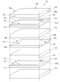
- FIG. 1B is a sectional view taken along line I-I in FIG. 1A of the laminated body in the L direction. It is a cross-sectional view in the W direction of the laminated body along the line II-II in FIG. 1A. It is a partial cross-sectional perspective view of the area
- FIG. 1C It is a partial cross-sectional perspective view of the region D (fourth side surface side) of the laminated body in FIG. 1C. It is an exploded perspective view which shows the modification of FIG. 1A. It is a partial cross-sectional perspective view which shows the modification of FIG. 2A. It is a partial cross-sectional perspective view which shows the modification of FIG. 2B. It is a partial cross-sectional perspective view which shows the modification of FIG. 3A. It is a partial cross-sectional perspective view which shows the modification of FIG. 3B. It is sectional drawing which shows the modification of FIG. 1B. It is a bird's-eye view which shows the result of having measured the side surface of the all-solid-state battery in an Example with the microscope.
- 9A to 9C are views for explaining a method of measuring the ten-point average roughness Rzjis of the side surface in the example. It is a graph which shows the relationship between the ten-point average roughness Rzjis measured in an Example, and the capacity retention rate.
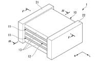
- an all-solid-state battery 1 is a perspective view of an all-solid-state battery according to an embodiment of the present invention
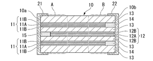
- FIG. 1B is a cross-sectional view in the L direction of the stack taken along line I-I in FIG. 1A
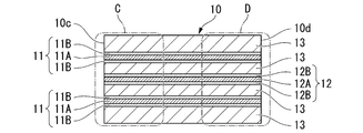
- FIG. 1C is a line II in FIG. 1A
- 7 is a cross-sectional view in the W direction of the laminated body along the line -II.
- an all-solid-state battery 1 includes a positive electrode layer 11 including a positive electrode current collector layer 11A and a positive electrode active material layer 11B, and a negative electrode including a negative electrode current collector layer 12A and a negative electrode active material layer 12B.
- the layer 12 and the layer 12 include a laminated body 10 that is alternately laminated via the solid electrolyte layer 13.
- the all-solid-state battery 1 is not particularly limited, but is preferably an all-solid-state secondary battery, and more preferably an all-solid-state lithium-ion secondary battery.
- the positive electrode layer 11 functions as a positive electrode
- the negative electrode layer 12 functions as a negative electrode.
- the present invention is not limited to this, and the negative electrode layer may be arranged at the position of the positive electrode layer 11 and the positive electrode layer may be arranged at the position of the negative electrode layer 12.
- the positive and negative of each electrode layer can be changed depending on which polarity is connected to the external terminal described later.
- a plurality of positive electrode layers 11 and a plurality of negative electrode layers 12 are provided, respectively, and by transferring lithium ions via the solid electrolyte between the positive electrode layers 11 and the negative electrode layers 12 arranged in close proximity, the all-solid-state battery 1 Is charged and discharged.
- the positive electrode layer 11 is connected to the external electrode 21, and the negative electrode layer 12 is connected to the external electrode 22.
- the external electrode 21 is formed in contact with the first side surface 10a of the stacked body 10 (the side surface where one end of the positive electrode layer 11 is exposed), and the external electrode 21 is the second side surface 10b of the stacked body 10 (one end of the negative electrode layer 12). It is formed in contact with the side surface where the portion is exposed (FIG. 1B).
- the external electrodes 21 and 22 are connected to external terminals (not shown) and are responsible for transferring and receiving electrons to the laminated body 10.
- the external electrodes 21, 22 are preferably made of a material having a high conductivity. For example, silver, gold, platinum, aluminum, copper, tin, nickel, gallium, indium, and alloys thereof can be used. Further, the external electrodes 21 and 22 may be formed in a multilayer structure, and may have, for example, a laminated structure in which a metal layer and a plating layer are laminated.
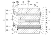
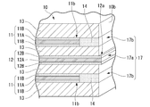
- FIG. 2A is a partial cross-sectional perspective view of a region A (first side face 10a side) of the laminated body 10 in FIG. 1B
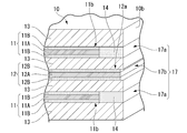
- FIG. 2B is a region B (second side face 10b side) portion of the laminated body 10 in FIG. 1B.
- the positive electrode layer 11 includes a first positive electrode end portion 11a exposed on the first side surface 10a of the stacked body 10 and a second positive electrode end portion 11b not exposed on the second side surface 10b opposite to the first side surface 10a.
- the negative electrode layer 12 has a first negative electrode end portion 12a exposed on the second side surface 10b of the stacked body 10 and a second negative electrode end portion 12b not exposed on the first side surface 10a of the stacked body 10.
- the laminated body 10 is disposed between the second positive electrode end portion 11b and the second side surface 10b, and is interposed between two adjacent solid electrolyte layers 13 and 13, the positive electrode margin layer 14, the second negative electrode end portion 12b, and the second negative electrode end portion 12b. It may have a negative electrode margin layer 15 which is arranged between one side surface 10a and is interposed between two adjacent solid electrolyte layers 13 and 13.
- the all-solid-state battery 1 includes a first uneven portion 16 formed on the first side surface 10a of the laminated body 10 and a second uneven portion 17 formed on the second side surface 10b of the laminated body 10.
- the "first concavo-convex portion 16 (second concavo-convex portion 17)" is, for example, a first concavo-convex strip portion (third) extending in a direction substantially perpendicular to the laminating direction of the laminated body 10 in a side view of the laminated body 10. 2 ridges and valleys).
- the first concavo-convex portion 16 (second concavo-convex portion 17) may be formed in a stripe shape on the first side surface 10a (second side surface 10b) of the stacked body 10.
- the first concavo-convex portion 16 is composed of first convex portions 16a and first concave portions 16b which are continuously provided alternately in the stacking direction of the laminated body 10.
- the second concave-convex portion 17 is composed of second convex portions 17 a and second concave portions 17 b that are alternately and continuously provided in the stacking direction of the laminated body 10.
- the first convex portion 16a of the first uneven portion 16 is formed by the first positive electrode end portion 11a, and the first concave portion 16b of the first uneven portion 16 is formed. It is formed by a solid electrolyte layer 13 and a negative electrode margin layer 15. Further, on the second side surface 10b of the laminated body 10, the second convex portion 17a of the second uneven portion 17 is formed by the first negative electrode end portion 12a, and the second concave portion 17b of the second uneven portion 17 is a solid electrolyte layer. It is formed by 13 and a positive electrode margin layer 14.
- the ten-point average roughness Rzjis of the first side surface 10a is preferably 1.0 ⁇ m or more.
- the ten-point average roughness Rzjis of the first side surface 10a is 1.0 ⁇ m or more, a sufficient buffering effect of volume expansion and contraction due to charging and discharging of the laminated body 10 can be obtained.
- the ten-point average roughness Rzjis of the first side surface 10a is less than 1.0 ⁇ m, the buffering effect of volume expansion and contraction cannot be obtained, and the cycle characteristics tend to deteriorate.
- the ten-point average roughness Rzjis of the first side surface 10a is preferably 12 ⁇ m or less.
- the ten-point average roughness Rzjis of the first side surface 10a is 12 ⁇ m or less, a sufficient buffering effect of volume expansion and contraction due to charging and discharging of the laminated body 10 can be obtained.
- the ten-point average roughness Rzjis of the first side surface 10a exceeds 12 ⁇ m, cracks are likely to occur due to volume expansion and contraction of the laminated body 10, and the cycle characteristics may deteriorate.
- the ten-point average roughness Rzjis of the first side surface 10a is more preferably 1.0 ⁇ m or more and 12 ⁇ m or less, further preferably 1.0 ⁇ m or more and 10 ⁇ m or less, and particularly preferably 3.0 ⁇ m or more 5 It is 0.0 ⁇ m or less.
- the ten-point average roughness Rzjis of the second side surface 10b is preferably 1.0 ⁇ m or more.
- the ten-point average roughness Rzjis of the second side surface 10b is 1.0 ⁇ m or more, a sufficient buffering effect of volume expansion / contraction due to charging / discharging of the laminated body 10 can be obtained.
- the ten-point average roughness Rzjis of the second side surface 10b is less than 1.0 ⁇ m, the buffering effect of volume expansion and contraction cannot be obtained, and the cycle characteristics tend to deteriorate.
- the ten-point average roughness Rzjis of the second side surface 10b is preferably 12 ⁇ m or less.
- the ten-point average roughness Rzjis of the second side surface 10b is 12 ⁇ m or less, a sufficient buffering effect of volume expansion and contraction due to charging and discharging of the laminated body 10 can be obtained.
- the ten-point average roughness Rzjis of the second side surface 10b exceeds 12 ⁇ m, cracks are likely to occur due to volume expansion and contraction of the laminated body 10, and the cycle characteristics may deteriorate.
- the ten-point average roughness Rzjis of the second side surface 10b is more preferably 1.0 ⁇ m or more and 12 ⁇ m or less, further preferably 1.0 ⁇ m or more and 10 ⁇ m or less, and particularly preferably 3.0 ⁇ m or more 5 It is 0.0 ⁇ m or less.
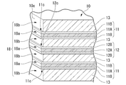
- FIG. 3A is a partial cross-sectional perspective view of a region C (third side face 10c side) of the laminated body 10 in FIG. 1C
- FIG. 3B is a region D (fourth side face 10d side) portion of the laminated body 10 in FIG. 1C. It is a cross-sectional perspective view.
- the laminate 10 has a third side surface 10c and a fourth side surface 10d located on the sides of the first side surface 10a and the second side surface 10b.
- the stacked body 10 is, for example, a rectangular parallelepiped, and the first side surface 10a and the second side surface 10b form an end surface in the L direction (longitudinal direction), and the third side surface 10c and the fourth side surface 10d form an end surface in the W direction (width direction). To do.
- the positive electrode layer 11 has a third positive electrode end 11c that is located on the side of the first positive electrode end 11a and the second positive electrode end 11b and is exposed on the third side surface 10c.
- the negative electrode layer 12 has a third negative electrode end portion 12c that is located on the side of the first negative electrode end portion 12a and the second negative electrode end portion 12b and is exposed on the third side surface 10c.
- the positive electrode layer 11 has a fourth positive electrode end 11d that is located on the side of the first positive electrode end 11a and the second positive electrode end 11b and is exposed on the fourth side surface 10d.
- the negative electrode layer 12 has a fourth negative electrode end portion 12d located on the side of the first negative electrode end portion 12a and the second negative electrode end portion 12b and exposed on the fourth side surface 10d.
- the all-solid-state battery 1 may include a third uneven portion 18 formed on the third side surface 10c of the stacked body 10 and a fourth uneven portion 19 formed on the fourth side surface 10d of the stacked body 10.
- the "third uneven portion 18 (fourth uneven portion 19)" is, for example, a third uneven strip portion (third uneven portion 19) extending in a direction substantially perpendicular to the stacking direction of the laminated body 10 in a side view of the laminated body 10. 4 ridges and valleys).
- the third concavo-convex portion 18 (fourth concavo-convex portion 19) may be formed in a striped pattern on the third side surface 10c (fourth side surface 10d) of the stacked body 10.
- the third concavo-convex portion 18 is composed of third convex portions 18a and third concave portions 18b that are provided alternately and continuously in the stacking direction of the laminated body 10.
- the fourth uneven portion 19 is composed of fourth convex portions 19a and fourth concave portions 19b that are provided alternately and continuously in the stacking direction of the stacked body 10.
- the third convex portion 18a of the third concave-convex portion 18 is formed by the third positive electrode end portion 11c and the third negative electrode end portion 12c, and the third concave-convex portion 18 is formed.
- the third recess 18 b of the solid electrolyte layer 13 can be formed.
- the third convex portion 18a of the third uneven portion 18 may be formed by either the third positive positive end portion 11c or the third negative negative end portion 12c.
- the fourth convex portion 19a of the fourth concave-convex portion 19 is formed by the fourth positive electrode end portion 11d and the fourth negative electrode end portion 12d, and
- the fourth recess 19b may be formed of the solid electrolyte layer 13.
- the fourth convex portion 19a of the fourth uneven portion 19 may be formed by either the fourth positive electrode end portion 11d or the fourth negative electrode end portion 12d.
- the ten-point average roughness Rzjis of the third side surface 10c and the fourth side surface 10d is preferably 1.0 ⁇ m or more, respectively.
- the ten-point average roughness Rzjis of the third side face 10c and the fourth side face 10d is 1.0 ⁇ m or more, it is possible to obtain a sufficient buffering effect for the volume expansion and contraction of the laminate 10 due to charge and discharge.
- the ten-point average roughness Rzjis of the third side surface 10c and the fourth side surface 10d is less than 1.0 ⁇ m, respectively, the buffer effect of volume expansion/contraction cannot be obtained, and the cycle characteristics are likely to deteriorate.
- the ten-point average roughness Rzjis of the third side surface 10c and the fourth side surface 10d is preferably 12 ⁇ m or less, respectively.
- the ten-point average roughness Rzjis of the third side face 10c and the fourth side face 10d is 12 ⁇ m or less, it is possible to obtain a sufficient buffering effect for the volume expansion and contraction of the laminate 10 due to charge and discharge.
- the ten-point average roughness Rzjis of the third side surface 10c and the fourth side surface 10d exceeds 12 ⁇ m, cracks are likely to occur due to volume expansion and contraction of the laminated body 10, and the cycle characteristics may deteriorate.
- the ten-point average roughness Rzjis of the third side surface 10c and the fourth side surface 10d is more preferably 1.0 ⁇ m or more and 12 ⁇ m or less, still more preferably 1.0 ⁇ m or more and 10 ⁇ m or less, and particularly preferably. It is 3.0 ⁇ m or more and 5.0 ⁇ m or less.
- the positive electrode current collector layer 11A and the negative electrode current collector layer 12A are composed of at least one substance having high conductivity.
- the highly conductive substance is, for example, at least one of silver (Ag), palladium (Pd), gold (Au), platinum (Pt), aluminum (Al), copper (Cu), and nickel (Ni). Examples thereof include metals or alloys containing one metal element and non-metals of carbon (C). Of these metal elements, copper and nickel are preferable in consideration of manufacturing cost in addition to high conductivity. Furthermore, copper is less likely to react with the positive electrode active material, the negative electrode active material and the solid electrolyte.
- the internal resistance of the all-solid-state battery 1 can be reduced.
- the substances constituting the positive electrode current collector layer 11A and the negative electrode current collector layer 12A may be the same or different.
- the thickness of the positive electrode current collector layer 11A and the negative electrode current collector layer 12A is not particularly limited, but is, for example, 0.5 ⁇ m or more and 30 ⁇ m or less.
- the positive electrode active material layer 11B is formed on one side or both sides of the positive electrode current collector layer 11A.
- the positive electrode layer 11 located at the uppermost layer in the stacking direction of the laminated body 10 does not have the negative electrode layer 12 facing each other on the upper side in the stacking direction. Therefore, in the positive electrode layer 11 located at the uppermost layer of the all-solid-state battery 1, the positive electrode active material layer 11B need only be on one side on the lower side in the stacking direction, but there is no particular problem even if it is on both sides.
- the negative electrode active material layer 12B is also formed on one side or both sides of the negative electrode current collector layer 12A, similarly to the positive electrode active material layer 11B.
- the thickness of the positive electrode active material layer 11B and the negative electrode active material layer 12B is preferably in the range of 0.5 ⁇ m or more and 5.0 ⁇ m or less.
- the positive electrode active material layer 11B and the negative electrode active material layer 12B contain a positive electrode active material or a negative electrode active material that transfer lithium ions and electrons, respectively.
- a binder, a conductive auxiliary agent, or the like may be included.
- the positive electrode active material and the negative electrode active material are preferably capable of efficiently inserting and releasing lithium ions.
- the active materials constituting the positive electrode active material layer 11B or the negative electrode active material layer 12B there is no clear distinction between the active materials constituting the positive electrode active material layer 11B or the negative electrode active material layer 12B, and the potentials of the two types of compounds are compared, and a compound showing a more noble potential is used as the positive electrode active material. A compound showing a low potential can be used as the negative electrode active material. Therefore, the active materials will be collectively described below.
- a transition metal oxide, a transition metal composite oxide, or the like can be used as the active material.
- the positive electrode current collector layer 11A and the negative electrode current collector layer 12A may contain a positive electrode active material and a negative electrode active material, respectively.
- the content ratio of the active material contained in each current collector is not particularly limited as long as it functions as a current collector.
- the volume ratio of the positive electrode current collector/positive electrode active material or the negative electrode current collector/negative electrode active material is preferably in the range of 90/10 to 70/30.
- the positive electrode current collector layer 11A and the negative electrode current collector layer 12A contain the positive electrode active material and the negative electrode active material, respectively, the positive electrode current collector layer 11A, the positive electrode active material layer 11B, the negative electrode current collector layer 12A, and the negative electrode active material are contained. Adhesion with layer 12B is improved.
- the solid electrolyte layer 13 is located between the positive electrode active material layer 11B and the negative electrode active material layer 12B. Further, the solid electrolyte layer 13 is composed of an uppermost layer in the stacking direction of the stack 10 (one outermost layer of the stack 10) and a lowermost layer in the stacking direction of the stack 10 (the other outermost layer of the stack 10). May be located. In this case, both the uppermost layer and the lowermost layer of the laminated body 10 are composed of the solid electrolyte layer 13. However, the positive electrode layer 11 may be located at the uppermost layer in the stacking direction of the stacked body 10, and the negative electrode layer 12 may be located at the lowermost layer in the stacking direction of the stacked body 10.
- the uppermost layer of the laminated body 10 is composed of the positive electrode layer 11
- the lowermost layer of the laminated body 10 is composed of the negative electrode layer 12.
- protective layers may be located at the uppermost layer and the lowest layer in the stacking direction of the laminated body 10. In that case, the uppermost layer and the lowermost layer of the laminated body 10 are configured by protective layers.
- Solid electrolytes include, for example, perovskite-type compounds such as La 0.5 Li 0.5 TiO 3 , ricicon-type compounds such as Li 14 Zn (GeO 4 ) 4, and garnet-type compounds such as Li 7 La 3 Zr 2 O 12 .
- LiZr 2 (PO 4 ) 3 Li 1.3 Al 0.3 Ti 1.7 (PO 4 ) 3 and Li 1.5 Al 0.5 Ge 1.5 (PO 4 ) 3 and the like
- Nasicon type compounds Thiolysicon type compounds such as Li 3.25 Ge 0.25 P 0.75 S 4 and Li 3 PS 4
- glass compounds such as Li 2 S—P 2 S 5 and Li 2 O—V 2 O 5 —SiO 2
- At least one selected from the group consisting of phosphoric compounds such as Li 3 PO 4 , Li 3.5 Si 0.5 P 0.5 O 4, and Li 2.9 PO 3.3 N 0.46. Is desirable.
- the solid electrolyte layer 13 is preferably selected according to the active material used for the positive electrode layer 11 and the negative electrode layer 12.
- the solid electrolyte layer 13 more preferably contains the same element as the element forming the active material.
- the bonding at the interface between the positive electrode active material layer 11B and the negative electrode active material layer 12B and the solid electrolyte layer 13 becomes strong. Further, the contact area at the interface between the positive electrode active material layer 11B and the negative electrode active material layer 12B and the solid electrolyte layer 13 can be widened.
- the thickness of the solid electrolyte layer 13 located between the positive electrode active material layer 11B and the negative electrode active material layer 12B is preferably in the range of 0.5 ⁇ m or more and 20.0 ⁇ m or less.
- the thickness of the solid electrolyte layer 13 between the positive electrode active material layer 11B and the negative electrode active material layer 12B is preferably in the range of 0.5 ⁇ m or more and 20.0 ⁇ m or less.
- the thickness of the solid electrolyte layer 13 located at the uppermost layer and the lowest layer in the laminating direction of the laminated body 10 is not particularly limited, but can be, for example, 0.5 ⁇ m or more and 20 ⁇ m or less.
- the positive electrode margin layer 14 may be arranged side by side with the positive electrode layer 11 at substantially the same position with respect to the stacking direction of the laminated body 10 (FIG. 2B).
- the positive electrode margin layer 14 may extend from the second positive electrode end 11b to the second side surface 10b.
- the negative electrode margin layer 15 may also be arranged side by side with the negative electrode layer 12 at substantially the same position with respect to the stacking direction of the laminated body 10 (FIG. 2A).
- the negative electrode margin layer 15 may extend from the second negative electrode end portion 12b to the first side surface 10a.
- the positive electrode margin layer 14 is provided only on the side of the second positive electrode end portion 11b of the first positive electrode end portion 11a to the fourth positive electrode end portion 11d of the positive electrode layer 11, but Not limited.
- the positive electrode margin layer 14-1 is provided between the second positive electrode end portion 11b of the positive electrode layer 11 and the second side surface 10b, between the third positive electrode end portion 11c and the third side surface 10c, and It may be provided between the fourth positive electrode end 11d and the fourth side surface 10d.
- the positive electrode margin layer 14-1 has a U-shape in a plan view, and only the first positive electrode end portion 11a of the positive electrode layer 11 is exposed on the first side surface 10a of the laminated body 10.
- the negative electrode margin layer 15 is provided only on the side of the second negative electrode end portion 12b of the first negative electrode end portion 12a to the fourth negative electrode end portion 12d of the negative electrode layer 12, but is not limited to this. ..
- the negative electrode margin layer 15-1 includes the second negative electrode end portion 12b and the first side surface 10a, the third negative electrode end portion 12c and the third side surface 10c, and the fourth negative electrode end. It may be provided between the portion 12d and the fourth side face 10d.
- the negative electrode margin layer 15-1 has a U-shape in a plan view, and only the first negative electrode end portion 12a of the negative electrode layer 12 is exposed on the second side surface 10b of the laminated body 10. In FIG.
- only the first positive electrode end portion 11a of the positive electrode layer 11 is exposed to the first side face 10a of the stacked body 10, and only the first negative electrode end portion 12a of the negative electrode layer 12 is stacked. Although it is exposed to the second side surface 10b of 10, it is not limited to this.
- the laminated body 10 only the first positive electrode end portion 11a of the positive electrode layer 11 is exposed to the first side face 10a, or only the first negative electrode end portion 12a of the negative electrode layer 12 is the first positive electrode end portion 11a of the laminated body 10. It may be exposed on the two side surfaces 10b.
- the positive electrode margin layers 14 and 14-1 are preferably provided to eliminate the step between the adjacent solid electrolyte layers 13 and 13 and the positive electrode layer 11, and the negative electrode margin layers 15 and 15-1 are adjacent to the solid electrolyte layers. It is preferably provided in order to eliminate the step between the layers 13 and 13 and the negative electrode layer 12. Therefore, it is preferable that the positive electrode margin layers 14 and 14-1 be formed between the adjacent solid electrolyte layers 13 and 13 with a thickness substantially equal to that of the positive electrode layer 11.
- the presence of the positive electrode margin layers 14 and 14-1 and the negative electrode margin layers 15 and 15-1 eliminates the step between the solid electrolyte layer 13 and the positive electrode layer 11 and the step between the solid electrolyte layer 13 and the negative electrode layer 12. The denseness between the solid electrolyte layer 13 and each electrode layer is increased, and delamination and warpage due to firing of the all-solid-state battery 1 are less likely to occur.
- the materials constituting the positive electrode margin layers 14, 14-1 and the negative electrode margin layers 15, 15-1 contain a solid electrolyte.
- the solid electrolyte contained in the positive electrode margin layer 14 and the negative electrode margin layer 15 may be the same as or different from the solid electrolyte contained in the solid electrolyte layer 13, but preferably contains the same material.
- a perovskite-type compound such as La 0.5 Li 0.5 TiO 3
- a ricicon-type compound such as Li 14 Zn (GeO 4 ) 4
- a garnet-type compound such as Li 7 La 3 Zr 2 O 12
- a Nasicon-type compound such as Li 1.3 Al 0.3 Ti 1.7 (PO 4 ) 3 or Li 1.5 Al 0.5 Ge 1.5 (PO 4 ) 3
- Li 3 .25 Chiorishikon type compounds such as Ge 0.25 P 0.75 S 4 and Li 3 PS 4, Li 2 S -P 2 S 5 and Li 2 O-V 2 O 5 glass compounds such -SiO 2, Li 3
- a method for manufacturing the all-solid-state battery 1 will be described.
- a simultaneous firing method may be used, or a sequential firing method may be used.
- the co-fired method is a method in which the materials forming each layer are laminated and then a laminated body is produced by batch firing.
- the sequential firing method is a method in which each layer is produced in order, and a firing step is performed each time each layer is produced.
- the simultaneous firing method is used, the laminated body 10 can be formed in a smaller number of work steps as compared with the case where the sequential firing method is used. Further, when the co-fired method is used, the obtained laminated body 10 becomes denser than when the sequential firing method is used.
- a case where the laminated body 10 is manufactured by using the co-fired method will be described as an example.
- the co-fired method includes a step of preparing a paste of each material constituting the laminated body 10, a step of applying and drying the paste to prepare a green sheet, and a step of laminating the green sheet to form a laminated sheet, which is fired at the same time. And the process. First, each of the positive electrode current collector layer 11A, the positive electrode active material layer 11B, the solid electrolyte layer 13, the negative electrode active material layer 12B, the negative electrode current collector layer 12A, the positive electrode margin layer 14, and the negative electrode margin layer 15 which constitute the laminated body 10. Make the material into a paste.
- a paste can be obtained by mixing powders of each material with a vehicle.
- vehicle is a general term for a medium in a liquid phase.
- the vehicle contains a solvent and a binder.
- a sintering modifier can be added to the positive electrode current collector layer 11A paste, the positive electrode active material layer 11B paste, the negative electrode current collector layer 12A paste, and the negative electrode active material layer 12B paste.
- the sintering modifier is, for example, an inorganic material having a melting point higher than that of the main component of the current collector, and is, for example, a particulate metal simple substance, compound, or alloy. This makes it possible to moderate the contraction of the positive electrode current collector layer 11A and the negative electrode current collector layer 12A in the subsequent firing step, and to form the first unevenness portion 16 on the first side face 10a of the laminate 10, and The second uneven portion 17 can be formed on the second side surface 10b.
- the sintering easing agent may be added to either the paste of the positive electrode current collector layer 11A or the paste of the negative electrode current collector layer 12A.
- a sintering accelerator may be added to the paste for the solid electrolyte layer 13, the paste for the positive electrode margin layer 14, and the paste for the negative electrode margin layer 15.
- the sintering accelerator is, for example, a commonly used sintering aid.
- the shrinkage of the solid electrolyte layer 13, the positive electrode margin layer 14, and the negative electrode margin layer 15 can be promoted in the subsequent firing step, and as a result, the first uneven portion 16 is formed on the first side surface 10a of the stacked body 10.
- the second uneven portion 17 can be formed on the second side surface 10b. Further, by using the sintering alleviating agent and the sintering accelerator in combination, the first uneven portion 16 and the second uneven portion 17 can be easily formed.
- a paste for the positive electrode current collector layer 11A a paste for the positive electrode active material layer 11B, a paste for the solid electrolyte layer 13, a paste for the negative electrode active material layer 12B, and a paste for the negative electrode current collector layer 12A are prepared.
- the laminated sheet can be produced, for example, by producing a positive electrode active material layer unit and a negative electrode active material layer unit described below and laminating them.
- a paste for the solid electrolyte layer 13 is applied on a base material such as a PET film by a doctor blade method and dried to form a sheet-like solid electrolyte layer 13.
- the paste for the positive electrode active material layer 11B is printed on the solid electrolyte layer 13 by screen printing and dried to form the positive electrode active material layer 11B.
- the paste for the positive electrode current collector layer 11A is printed by screen printing on the positive electrode active material layer 11B and dried to form the positive electrode current collector layer 11A.
- the paste for the positive electrode active material layer 11B is printed on the positive electrode current collector layer 11A by screen printing and dried to form the positive electrode active material layer 11B.
- the paste for the positive electrode margin layer 14 is printed by screen printing on the portion on the solid electrolyte layer 13 where the positive electrode active material layer 11B, the positive electrode current collector layer 11A and the positive electrode active material layer 11B are not formed. And dried to form the positive electrode margin layer 14.
- the positive electrode margin layer 14-1 and the negative electrode margin layer 15-1 are also formed in the same process as the positive electrode margin layer 14 and the negative electrode margin layer 15, and thus the description thereof will be omitted.
- the positive electrode active material layer unit is a laminated sheet in which the solid electrolyte layer 13 / positive electrode active material layer 11B / positive electrode current collector layer 11A / positive electrode active material layer 11B are laminated in this order.
- a negative electrode active material layer unit is produced by the same procedure.
- This negative electrode active material layer unit is a laminated sheet in which a solid electrolyte layer 13 / a negative electrode active material layer 12B / a negative electrode current collector layer 12A / a negative electrode active material layer 12B are laminated in this order.
- the positive electrode active material layer unit and the negative electrode active material layer unit are laminated.
- the positive electrode active material layer 11B of the positive electrode active material layer unit and the solid electrolyte layer 13 of the negative electrode active material layer unit are laminated so as to be in contact with each other, or the solid electrolyte layer 13 of the positive electrode active material layer unit and the negative electrode active material layer 13 are The material layer unit is laminated so as to be in contact with the negative electrode active material layer 12B.
- the negative electrode active material layer 12B/negative electrode current collector layer 12A/negative electrode active material layer 12B/solid electrolyte layer 13/positive electrode active material layer 11B/positive electrode current collector layer 11A/positive electrode active material layer 11B/solid electrolyte layer 13 To obtain a laminated sheet in which the layers are laminated in this order.
- the positive electrode active material layer unit and the negative electrode active material layer unit are alternately stacked, and a solid electrolyte sheet having a predetermined thickness is applied to the uppermost layer and the lowermost layer of the laminated body in which the positive electrode active material layer unit and the negative electrode active material unit are stacked. Further, the sheets are stacked to form a laminated sheet.
- the produced laminated sheets are collectively pressure-bonded.
- the pressure bonding is preferably performed while heating.
- the heating temperature at the time of pressure bonding is, for example, 40 to 95°C.
- the crimped laminated sheet green sheet laminated body
- the crimped laminated sheet is heated to 500 ° C. to 750 ° C. in an atmosphere of nitrogen, hydrogen and water vapor to remove the binder.
- a sintered body is obtained by heating to 600 ° C. to 1000 ° C. in a nitrogen, hydrogen and steam atmosphere and firing.
- the firing time is, for example, 0.1 to 3 hours.
- the first uneven portion 16 and the second uneven portion 17 are formed by using the shrinkage reducing agent and / or the sintering accelerator, but the present invention is not limited to this.
- the first uneven portion 16 and the second uneven portion 17 may be formed by processing with a laser beam or processing using a mold having an uneven shape.
- a laser such as an ultrashort pulse laser having a beam spot diameter of micro order and a pulse width of picosecond to nanosecond order on the first side surface 10a of the sintered body (laminated body 10).
- a groove having a width and a depth of micro-order is formed, thereby forming the first uneven portion 16.
- the second side surface 10b of the sintered body (laminated body 10) is irradiated with the same laser light as described above, and a groove is formed by sweeping in a direction substantially perpendicular to the stacking direction, whereby the second unevenness is formed.
- the part 17 is formed.
- the solid electrolyte layer 13 and the negative electrode margin layer 15 on the first side surface 10a with laser light.
- the first convex portion 16a of the first uneven portion 16 is formed by the first positive electrode end portion 11a
- the first concave portion 16b of the first uneven portion 16 is formed by the solid electrolyte layer 13 and the negative electrode margin layer 15. be able to.
- the second convex portion 17a of the second uneven portion 17 is formed by the first negative electrode end portion 12a, and the second concave portion 17b of the second uneven portion 17 is formed by the solid electrolyte layer 13 and the positive electrode margin layer 14. be able to.
- a groove is formed by irradiating the third side surface 10c of the sintered body (laminated body 10) with the first uneven portion 16 having a micro-order spot diameter and sweeping in a direction substantially perpendicular to the stacking direction, This may form the first uneven portion 16.
- the second side surface 10b of the sintered body (laminated body 10) is irradiated with the same laser light as described above, and a groove is formed by sweeping in a direction substantially perpendicular to the stacking direction, whereby the second unevenness is formed.
- the part 17 may be formed.
- the laser light may be applied to the solid electrolyte layer 13 on the third side surface 10c and/or the solid electrolyte layer 13 on the fourth side surface 10d.
- the third convex portion 18a of the third uneven portion 18 is formed by the third positive electrode end portion 11c and the third negative electrode end portion 12c
- the third concave portion 18b of the third uneven portion 18 is formed by the solid electrolyte layer 13.
- the fourth convex portion 19a of the fourth uneven portion 19 is formed by the fourth positive electrode end portion 11d and the fourth negative electrode end portion 12d
- the fourth concave portion 19b of the fourth uneven portion 19 is formed by the solid electrolyte layer 13. can do.
- the obtained sintered body may be placed in a cylindrical container together with an abrasive such as alumina and barrel-polished. As a result, the corners of the laminated body 10 can be chamfered.
- the laminate 10 may be polished by sandblasting. This method is preferable because only a specific part can be scraped.
- the laminate 10 is obtained through the above steps.
- the external electrodes 21 and 22 are formed on the first side surface 10a and the second side surface 10b of the laminated body 10 manufactured by the above procedure.
- the external electrodes 21 and 22 are formed in a single layer structure or a multilayer structure obtained by a known method. As a result, the all-solid-state battery 1 including the laminated body 10 is manufactured.
- the all-solid-state battery 1 includes the first uneven portion 16 formed on the first side surface 10 a of the stacked body 10 and the first uneven portion 16 formed on the second side surface 10 b of the stacked body 10. Since the two uneven portions 17 are provided, the volume expansion and contraction of the laminated body 10 due to charge and discharge is sufficiently relaxed, cracks due to the volume expansion and contraction are less likely to occur, and excellent cycle characteristics can be obtained.
- the all-solid-state battery 1 includes a first uneven portion 16 and a second uneven portion 17, but is not limited to this, and the first uneven portion 16 formed on the first side surface 10a of the laminated body 10 and the first uneven portion 10 of the laminated body 10. Any of the second uneven portions 17 formed on the two side surfaces 10b may be provided. With this configuration, the same effect as described above can be obtained.
- the all-solid-state battery 1 since the all-solid-state battery 1 includes a third uneven portion 18 formed on the third side surface 10c of the laminated body 10 and a fourth uneven portion 19 formed on the fourth side surface 10d of the laminated body 10, it is charged and discharged.
- the volume expansion and contraction of the laminated body 10 accompanying the above is further relaxed, and more excellent cycle characteristics can be obtained.
- the all-solid-state battery 1 includes, but is not limited to, the third uneven portion 18 and the fourth uneven portion 19, and the third uneven portion 18 formed on the third side surface 10c of the laminated body 10 and the first of the laminated body 10. Any of the fourth uneven portions 19 formed on the four side surfaces 10d may be provided. With this configuration, the same effect as described above can be obtained. Further, for convenience of explanation, the third uneven portion 18 and the fourth uneven portion 19 have been described separately, but since the laminated body 10 is usually formed symmetrically with respect to the center position in the W direction, the fourth uneven portion is described. The configuration of the portion 19 is the same as the configuration of the third uneven portion 18.
- the uneven portion in the all-solid-state battery 1 is formed for each type of layer, but not all layers need to form the uneven portion.
- the recesses or protrusions are preferably formed by 60% or more of the total number of each layer, and more preferably 80% or more of the total number of each layer.
- FIG. 5A is a partial cross-sectional perspective view showing a modified example of FIG. 2A
- FIG. 5B is a partial cross-sectional perspective view showing a modified example of FIG. 2B.
- the convex portions and the members constituting the convex portions of the first concave-convex portion 16 to the fourth concave-convex portion 19 are different from the above-described embodiment.
- the first convex portion 16a of the first uneven portion 16 is formed by the solid electrolyte layer 13 and the negative electrode margin layer 15, and the first The first concave portion 16b of the uneven portion 16 is formed by the first positive electrode end portion 11a.
- the second convex portion 17 a of the second concave-convex portion 17 is formed by the solid electrolyte layer 13 and the positive electrode margin layer 14, and the second convex-concave portion 17 is formed.
- the second recess 17b of the above is formed by the first negative electrode end portion 12a.
- the ten-point average roughness Rzjis of the first side surface 10a is preferably 1.0 ⁇ m or more, more preferably 1.0 ⁇ m or more and 12 ⁇ m or less, further preferably from the same viewpoint as the above embodiment. Is 1.0 ⁇ m or more and 10 ⁇ m or less, and particularly preferably 3.0 ⁇ m or more and 5.0 ⁇ m or less.
- the ten-point average roughness Rzjis of the second side surface 10b is preferably 1.0 ⁇ m or more, more preferably 1.0 ⁇ m or more and 12 ⁇ m or less, still more preferably 1.0 ⁇ m or more, from the same viewpoint as the above embodiment. It is 10 ⁇ m or less, and particularly preferably 3.0 ⁇ m or more and 5.0 ⁇ m or less.
- FIG. 6A is a partial cross-sectional perspective view showing a modified example of FIG. 3A
- FIG. 6B is a partial cross-sectional perspective view showing a modified example of FIG. 3B.
- the third convex portion 18a of the third concave-convex portion 18 is formed of the solid electrolyte layer 13, and the third convex portion 18a of the third concave-convex portion 18 is formed.
- the three recesses 18b can be formed by the third positive electrode end 11c and the third negative electrode end 12c.
- the third convex portion 18a of the third uneven portion 18 may be formed by either the third positive positive end portion 11c or the third negative negative end portion 12c.
- the fourth convex portion 19a of the fourth uneven portion 19 is formed by the solid electrolyte layer 13, and the fourth concave portion 19b of the fourth uneven portion 19 is formed by the fourth positive electrode end portion 11d and The fourth negative electrode end portion 12d may be formed.
- the fourth convex portion 19a of the fourth uneven portion 19 may be formed by either the fourth positive electrode end portion 11d or the fourth negative electrode end portion 12d.
- the ten-point average roughness Rzjis of the third side surface 10c is preferably 1.0 ⁇ m or more, more preferably 1.0 ⁇ m or more and 12 ⁇ m or less, further preferably from the same viewpoint as the above embodiment. Is 1.0 ⁇ m or more and 10 ⁇ m or less, and particularly preferably 3.0 ⁇ m or more and 5.0 ⁇ m or less.
- the ten-point average roughness Rzjis of the fourth side surface 10d is preferably 1.0 ⁇ m or more, more preferably 1.0 ⁇ m or more and 12 ⁇ m or less, still more preferably 1.0 ⁇ m or more, from the same viewpoint as the above embodiment. It is 10 ⁇ m or less, and particularly preferably 3.0 ⁇ m or more and 5.0 ⁇ m or less.
- a shrinkage easing agent and / or the above-mentioned sintering accelerator may be used as in the above-described embodiment, or processing by laser light is performed. Alternatively, processing may be performed using a mold having an uneven shape.
- the paste for the positive electrode current collector layer 11A, the paste for the positive electrode active material layer 11B, the paste for the negative electrode current collector layer 12A, and the negative electrode are used in the step of forming the laminate 10.
- a sintering accelerator can be added to the paste for the active material layer 12B.
- a shrinkage reducing agent may be added to the paste for the solid electrolyte layer 13, the paste for the positive electrode margin layer 14, and the paste for the negative electrode margin layer 15.
- the laser light is applied to the positive electrode layer 11 on the first side surface 10a and the negative electrode layer 12 on the second side surface 10b.
- the first convex portion 16a of the first uneven portion 16 is formed by the solid electrolyte layer 13 and the negative electrode margin layer 15, and the first concave portion 16b of the first uneven portion 16 is formed by the first positive electrode end portion 11a.
- the second convex portion 17a of the second uneven portion 17 is formed by the solid electrolyte layer 13 and the positive electrode margin layer 14, and the second concave portion 17b of the second uneven portion 17 is formed by the first negative electrode end portion 12a.
- the laser beam may be applied to the positive electrode layer 11 on the third side surface 10c and / or the negative electrode layer 12 on the fourth side surface 10d.
- the third convex portion 18a of the third uneven portion 18 is formed by the solid electrolyte layer 13
- the third concave portion 18b of the third uneven portion 18 is formed by the third positive electrode end portion 11c and the third negative electrode end portion 12c.
- the fourth convex portion 19a of the fourth uneven portion 19 is formed by the solid electrolyte layer 13, and the fourth concave portion 19b of the fourth uneven portion 19 is formed by the fourth positive electrode end portion 11d and the fourth negative electrode end portion 12d. can do.
- the all-solid-state battery 1 is formed on the first uneven portion 16 formed on the first side surface 10a of the laminated body 10 and the second side surface 10b formed on the second side surface 10b of the laminated body 10. Since the uneven portion 17 is provided, the volume expansion and contraction of the laminated body 10 due to charge and discharge is sufficiently relaxed, cracks due to the volume expansion and contraction are less likely to occur, and excellent cycle characteristics can be obtained.
- FIG. 7 is a cross-sectional view showing a modified example of FIG. 1B.
- FIG. 7 is different from the cross-sectional view shown in FIG. 1B in that the laminated body 10 does not have the positive electrode margin layer 14 and the negative electrode margin layer 15.
- Other configurations are the same as those of the laminated body 10 of the above embodiment, and the description thereof will be omitted.
- the first convex portion 16a of the first uneven portion 16 is formed by the first positive electrode end portion 11a, and the first concave portion 16b of the first uneven portion 16 is formed. It is formed only by the solid electrolyte layer 13. Further, on the second side surface 10b of the laminated body 10, the second convex portion 17a of the second uneven portion 17 is formed by the first negative electrode end portion 12a, and the second concave portion 17b of the second uneven portion 17 is a solid electrolyte layer. It is formed by only 13.
- the laminated body 10 in this modification can be formed by adhering two adjacent solid electrolyte layers 13 and 13 to each other. In this modification, it is difficult to eliminate the step between the positive electrode layer 11 or the negative electrode layer 12 and the solid electrolyte layer 13, but the formation of the positive electrode margin layer 14 and the negative electrode margin layer 15 becomes unnecessary, so that the process can be simplified. it can.
- Example 1 to 6 Copper as the cathode current collector layer, Li 3 V 2 (PO 4 ) 3 as the positive electrode active material layer, copper as a negative electrode collector layer, Li 3 V 2 as the negative electrode active material layer (PO 4) 3, as a solid electrolyte layer , Li 1.3 Al 0.3 Ti 1.7 ( PO 4) 3, Li 1.3 Al 0.3 Ti 1.7 (PO 4) as a positive electrode margin layer 3, Li 1.3 Al as a negative electrode margin layer Using 0.3 Ti 1.7 (PO 4 ) 3 , an all-solid-state battery element body (laminate) having a size of 4.80 mm ⁇ 3.30 mm ⁇ 1.22 mm was produced by the above-described manufacturing method.
- the first concave-convex portion and the second concave-convex portion were formed on the two side faces (the first side face and the second side face) in the L direction of the laminate by processing with laser light.
- the first convex portion was formed of the positive electrode layer
- the first concave portion was formed of the solid electrolyte layer and the negative electrode margin layer.
- the second convex portion was formed of the negative electrode layer
- the second concave portion was formed of the solid electrolyte layer and the positive electrode margin layer.
- the average value of the ten-point average roughness Rzjis of the first uneven portion on the first side surface of the laminate and the ten-point average roughness Rzjis of the second uneven portion on the second side surface is The values shown in Table 1 were used. Then, an external electrode was formed on the first side surface side and the second side surface side of the laminated body by a known method to manufacture an all-solid-state battery.
- Example 7 to 12 An all-solid-state battery was manufactured in the same manner as in Examples 1 to 6 except that the first uneven portion was formed on one side surface (only the first side surface) in the L direction of the laminate.
- the first concavo-convex portion and the second concavo-convex portion are formed on the two side faces (first side face and second side face) in the L direction of the laminate, and the third concavo-convex portion and the second concavo-convex portion are formed on the second side face (third side face and fourth side face) in the W direction.
- An all-solid-state battery was produced in the same manner as in Examples 1 to 6 except that the fourth uneven portion was formed.
- the third convex portion was formed of the positive electrode layer and the negative electrode layer, and the third concave portion was formed of the solid electrolyte layer.
- the fourth convex portion was formed of the positive electrode layer and the negative electrode layer, and the fourth concave portion was formed of the solid electrolyte layer.
- the average value of the ten-point average roughness Rzjis is the ten-point average roughness Rzjis of the first uneven portion on the first side surface of the laminate, the ten-point average roughness Rzjis of the second uneven portion on the second side surface, and the laminated value.
- the average value was taken from the ten-point average roughness Rzjis of the third uneven portion on the third side surface of the body and the ten-point average roughness Rzjis of the fourth uneven portion on the fourth side surface.
- the first convex portion is formed of the solid electrolyte layer and the negative electrode margin layer
- the first concave portion is formed of the positive electrode layer
- the second convex portion is formed of the solid electrolyte layer and the positive electrode margin layer.
- Laminates were produced in the same manner as in Examples 1 to 6 except that the positive electrode margin layer and the negative electrode margin layer were not formed. Further, on the first side surface, the first convex portion is formed of the positive electrode layer, the first concave portion is formed of the solid electrolyte layer, and on the second side surface, the second convex portion is formed of the negative electrode layer, and the second concave portion is formed.
- An all-solid-state battery was produced in the same manner as in Examples 1 to 6 except that the solid-state electrolyte layer was formed.
- the ten-point average roughness Rzjis is obtained by extracting only the reference length from the roughness curve in the direction of the average line and measuring from the average line of this extracted portion in the direction of longitudinal magnification of the highest peak to the fifth peak.
- the sum of the average absolute value of the altitude (Yp) and the average absolute value of the altitudes (Yv) of the valley bottoms from the lowest valley to the fifth valley was calculated, and this value was expressed in micrometers ( ⁇ m). The results are shown in Table 1.
- Capacity retention rate As cycle characteristics, a lead wire was attached to two external electrodes and a charge/discharge test was performed to measure the initial discharge capacity of the all-solid-state battery and the capacity retention rate after 1000 cycles. The measurement conditions were that the current during charging and discharging was 0.2 ⁇ A, and the final voltages during charging and discharging were 1.6V and 0V, respectively. The capacity at the time of the first discharge was defined as the initial discharge capacity, and the discharge capacity at the 1000th cycle was divided by the initial discharge capacity to obtain the capacity retention rate. The results are shown in Table 1. Further, FIG. 10 shows the relationship between the ten-point average roughness Rzjis measured in the examples and the capacity retention rate.
- the Rzjis is in the range of 0.1 ⁇ m or more and 12 ⁇ m or less, and the capacity retention rate when the uneven portion is formed on only one side surface of the laminated body is the capacity retention rate of Comparative Example 1 having no uneven portion. It was found that it was higher than the capacity retention rate and excellent cycle characteristics were obtained.
- the Rzjis is within the range of 0.1 ⁇ m or more and 12 ⁇ m or less, and the capacity retention rate when the uneven portions are formed on the four side surfaces of the laminated body is the capacity of Comparative Example 1 having no uneven portions. It was found that the rate was higher than the maintenance rate and excellent cycle characteristics were obtained. Further, comparing Examples 13 to 18 and Examples 7 to 12, when Rzjis has the same value, the capacity retention rate when the uneven portions are formed on the four side surfaces of the laminated body is such that the uneven portions are formed on only one side surface. It was found that the capacity retention rate was higher than that when formed.
- the Rzjis is in the range of 0.1 ⁇ m or more and 12 ⁇ m or less, and the capacity retention rate when the uneven portions are formed on the two side surfaces of the laminated body is the capacity of Comparative Example 1 having no uneven portions. It was found that the rate was higher than the maintenance rate and excellent cycle characteristics were obtained.
- the Rzjis is in the range of 0.1 ⁇ m or more and 12 ⁇ m or less, and the capacity retention rate when the uneven portions are formed on the two side surfaces of the laminated body is the capacity of Comparative Example 1 having no uneven portions. It was found that the rate was higher than the maintenance rate and excellent cycle characteristics were obtained. Further, when Examples 25 to 30 and Examples 1 to 6 are compared, when Rzjis has the same value, the capacity retention rate when the margin layer is formed is higher than the capacity retention rate when the margin layer is not formed. It turned out to be high.
- an all-solid-state battery that can sufficiently suppress volume expansion and contraction associated with a charge / discharge reaction and can obtain excellent cycle characteristics.
Landscapes
- Chemical & Material Sciences (AREA)
- General Chemical & Material Sciences (AREA)
- Engineering & Computer Science (AREA)
- Chemical Kinetics & Catalysis (AREA)
- Electrochemistry (AREA)
- Manufacturing & Machinery (AREA)
- General Physics & Mathematics (AREA)
- Condensed Matter Physics & Semiconductors (AREA)
- Inorganic Chemistry (AREA)
- Physics & Mathematics (AREA)
- Materials Engineering (AREA)
- Secondary Cells (AREA)
- Battery Electrode And Active Subsutance (AREA)
Abstract
この全固体電池(1)は、正極層(11)と負極層(12)とが、固体電解質層(13)を介して交互に積層された積層体(10)を備える。正極層(11)は、積層体(10)の第1側面(10a)に露出している第1正極端部(11a)を有する。負極層(12)は、積層体(10)の第1側面(10a)に露出しない第2負極端部(12b)を有する。全固体電池(1)は、積層体(10)の第1側面(10a)に形成された第1凹凸部(16)を備える。
Description
本発明は、全固体電池に関し、例えば、全固体リチウムイオン二次電池に関する。
本願は、2019年3月7日に、日本に出願された特願2019-041862号に基づき優先権を主張し、その内容をここに援用する。
本願は、2019年3月7日に、日本に出願された特願2019-041862号に基づき優先権を主張し、その内容をここに援用する。
近年、エレクトロニクス技術の発達はめざましく、携帯電子機器の小型軽量化、薄型化、多機能化が図られている。それに伴い、電子機器の電源となる電池に対し、小型軽量化、薄型化、信頼性の向上が強く望まれており、固体電解質から成る全固体型のリチウムイオン二次電池(以下、全固体電池)が注目されている。
従来、汎用的に使用されているリチウムイオン二次電池では、イオンを移動させるための媒体として有機溶媒等の電解質(電解液)が使用されている。しかし、上記構成の電池では、電解液が漏出するという危険性がある。また、電解液に用いられる有機溶媒等は可燃性物質であるため、電池の安全性をさらに高めることが求められている。
電池の安全性を高めるための一つの対策は、電解質として、電解液に代えて、固体電解質を用いることが提案されている。さらに、電解質として固体電解質を用いるとともに、その他の構成要素も固体で構成される全固体電池の開発が進められている。
固体電解質が高い伝導率を示すためには、高温で緻密化させるという焼結プロセスにおいて、固体電解質を緻密化させることで粒界抵抗を小さく抑えることが重要とされている。例えば、正極単位層と負極単位層とイオン伝導性無機物質層との積層体を一括焼成してなる全固体二次電池の発明が開示されており(特許文献1)、焼成における各層の収縮量の差異を小さくするように材料選択することにより、クラックのない積層体の作製方法が開示されている。一方、固体電解質グリーンシート又は固体電解質層と電極グリーンシートとを積層・焼成してなるリチウム電池において、固体電解質グリーンシート又は固体電解質層の少なくとも一面に、高融点の無機物質の粉末を含む収縮抑制層とを設けることにより、各層の割れや層間剥離を生じにくくすることが開示されている(特許文献2)。
しかしながら、上記従来の方法で製造した全固体電池では、充放電反応に伴う体積膨張収縮の抑制が十分とは言えず、内部応力が全固体電池内に生じることでクラックが発生する場合がある。その結果、内部抵抗が増大し、優れたサイクル特性が得られにくいという問題がある。
本発明は、上記の課題に鑑みてなされたものであり、その目的は、充放電反応に伴う体積膨張収縮を十分に抑制することができ、優れたサイクル特性が得られる全固体電池を提供することにある。
上記目的を達成するために、本発明は以下の手段を提供する。
[1]正極集電体層と正極活物質層を含む正極層と、負極集電体層と負極活物質層を含む負極層とが、固体電解質層を介して交互に積層された積層体を備え、
前記正極層は、前記積層体の第1側面に露出している第1正極端部と、前記第1側面とは反対側の第2側面に露出しない第2正極端部とを有し、
前記負極層は、前記積層体の前記第2側面に露出している第1負極端部と、前記積層体の前記第1側面に露出しない第2負極端部とを有し、
前記積層体は、前記積層体の前記第1側面に形成された第1凹凸部、及び前記積層体の前記第2側面に形成された第2凹凸部のうちの少なくとも一方を備える、全固体電池。
[1]正極集電体層と正極活物質層を含む正極層と、負極集電体層と負極活物質層を含む負極層とが、固体電解質層を介して交互に積層された積層体を備え、
前記正極層は、前記積層体の第1側面に露出している第1正極端部と、前記第1側面とは反対側の第2側面に露出しない第2正極端部とを有し、
前記負極層は、前記積層体の前記第2側面に露出している第1負極端部と、前記積層体の前記第1側面に露出しない第2負極端部とを有し、
前記積層体は、前記積層体の前記第1側面に形成された第1凹凸部、及び前記積層体の前記第2側面に形成された第2凹凸部のうちの少なくとも一方を備える、全固体電池。
[2]前記積層体は、さらに、
前記第2正極端部と前記第2側面の間に配置され、隣接する2つの前記固体電解質層間に介在する正極マージン層と、
前記第2負極端部と前記第1側面の間に配置され、隣接する2つの前記固体電解質層間に介在する負極マージン層と、を有する、上記[1]に記載の全固体電池。
前記第2正極端部と前記第2側面の間に配置され、隣接する2つの前記固体電解質層間に介在する正極マージン層と、
前記第2負極端部と前記第1側面の間に配置され、隣接する2つの前記固体電解質層間に介在する負極マージン層と、を有する、上記[1]に記載の全固体電池。
[3]前記積層体の積層方向に関して、前記第1側面の十点平均粗さRzjisが、1.0μm以上である、上記[2]に記載の全固体電池。
[4]前記第1凹凸部の第1凸部が、前記第1正極端部によって形成され、前記第1凹凸部の第1凹部が、前記固体電解質層及び前記負極マージン層によって形成されている、上記[2]又は[3]に記載の全固体電池。
[5]前記第1凹凸部の第1凸部が、前記固体電解質層及び前記負極マージン層によって形成され、前記第1凹凸部の第1凹部が、前記第1正極端部によって形成されている、上記[2]又は[3]に記載の全固体電池。
[6]前記積層体の積層方向に関して、前記第1側面の十点平均粗さRzjisが、12μm以下である、上記[3]~[5]のいずれかに記載の全固体電池。
[7]前記積層体の積層方向に関して、前記第2側面の十点平均粗さRzjisが、1.0μm以上である、上記[2]~[6]のいずれかに記載の全固体電池。
[8]前記第2凹凸部の第2凸部が、前記第1負極端部によって形成され、前記第2凹凸部の第2凹部が、前記固体電解質層及び前記正極マージン層によって形成されている、上記[2]~[7]のいずれかに記載の全固体電池。
[9]前記第2凹凸部の第2凸部が、前記固体電解質層及び前記正極マージン層によって形成され、前記第2凹凸部の第2凹部が、前記第1負極端部によって形成されている、上記[2]~[7]のいずれかに記載の全固体電池。
[10]前記積層体の積層方向に関して、前記第2側面の十点平均粗さRzjisが、12μm以下である、上記[7]~[9]のいずれかに記載の全固体電池。
[11]前記積層体の積層方向に関して、前記第1側面の十点平均粗さRzjisが、1.0μm以上である、上記[1]に記載の全固体電池。
[12]前記第1凹凸部の第1凸部が、前記第1正極端部によって形成され、前記第1凹凸部の第1凹部が、前記固体電解質層によって形成されている、上記[1]又は[11]に記載の全固体電池。
[13]前記第1凹凸部の第1凸部が、前記固体電解質層によって形成され、前記第1凹凸部の第1凹部が、前記第1正極端部によって形成されている、上記[1]又は[11]に記載の全固体電池。
[14]前記積層体の積層方向に関して、前記第1側面の十点平均粗さRzjisが、12μm以下である、上記[11]~[13]のいずれかに記載の全固体電池。
[15]前記積層体の積層方向に関して、前記第2側面の十点平均粗さRzjisが、1.0μm以上である、上記[1]及び[11]~[14]のいずれかに記載の全固体電池。
[16]前記第2凹凸部の第2凸部が、前記第1負極端部によって形成され、前記第2凹凸部の第2凹部が、前記固体電解質層によって形成されている、上記[1]及び[11]~[15]のいずれかに記載の全固体電池。
[17]前記第2凹凸部の第2凸部が、前記固体電解質層によって形成され、前記第2凹凸部の第2凹部が、前記第1負極端部によって形成されている、上記[1]及び[11]~[15]のいずれかに記載の全固体電池。
[18]前記積層体の積層方向に関して、前記第2側面の十点平均粗さRzjisが、12μm以下である、上記[15]~[17]のいずれかに記載の全固体電池。
[19]前記積層体は、前記第1側面と前記第2側面の側方に位置する第3側面を有し、
前記正極層は、前記第1正極端部と前記第2正極端部の側方に位置し、前記第3側面に露出する第3正極端部を有し、
前記負極層は、前記第1負極端部と前記第2負極端部の側方に位置し、前記第3側面に露出する第3負極端部を有し、
前記積層体の前記第3側面に形成された第3凹凸部を備える、上記[1]~[18]のいずれかに記載の全固体電池。
前記正極層は、前記第1正極端部と前記第2正極端部の側方に位置し、前記第3側面に露出する第3正極端部を有し、
前記負極層は、前記第1負極端部と前記第2負極端部の側方に位置し、前記第3側面に露出する第3負極端部を有し、
前記積層体の前記第3側面に形成された第3凹凸部を備える、上記[1]~[18]のいずれかに記載の全固体電池。
[20]前記積層体の積層方向に関して、前記第3側面の十点平均粗さRzjisが、1.0μm以上である、上記[19]に記載の全固体電池。
[21]前記第3凹凸部の第3凸部が、前記第3正極端部及び前記第3負極端部の少なくとも一方で形成され、前記第3凹凸部の第3凹部が、前記固体電解質層で形成されている、上記[19]又は[20]に記載の全固体電池。
[22]前記第3凹凸部の第3凸部が、前記固体電解質層で形成され、前記第3凹凸部の第3凹部が、前記第3正極端部及び前記第3負極端部の少なくとも一方で形成されている、上記[19]又は[20]に記載の全固体電池。
[23]前記積層体の積層方向に関して、前記第3側面の十点平均粗さRzjisが、12μm以下である、上記[20]~[22]のいずれかに記載の全固体電池。
本発明によれば、充放電反応に伴う体積膨張収縮を十分に抑制することができ、優れたサイクル特性が得られる全固体電池を提供することができる。
以下、本発明の実施形態について、図面を参照して詳細に説明する。以下の説明で用いる図面は、本実施形態の特徴をわかりやすくするために便宜上特徴となる部分を拡大して示している場合があり、各構成要素の寸法比率などは実際とは異なっていることがある。
以下の説明において例示される物質、寸法等は一例であって、本実施形態はそれらに限定されるものではなく、本発明の効果を奏する範囲で適宜変更して実施することが可能である。
以下の説明において例示される物質、寸法等は一例であって、本実施形態はそれらに限定されるものではなく、本発明の効果を奏する範囲で適宜変更して実施することが可能である。
[全固体電池の構成]
図1Aは、本発明の実施形態に係る全固体電池の斜視図であり、図1Bは、図1Aにおける線I―Iに沿う積層体のL方向断面図、図1Cは、図1Aにおける線II―IIに沿う積層体のW方向断面図である。
図1A~図1Cに示すように、全固体電池1は、正極集電体層11Aと正極活物質層11Bを含む正極層11と、負極集電体層12Aと負極活物質層12Bを含む負極層12とが、固体電解質層13を介して交互に積層された積層体10を備えている。全固体電池1は、特に制限されないが、全固体二次電池であるのが好ましく、全固体リチウムイオン二次電池であるのがより好ましい。
図1Aは、本発明の実施形態に係る全固体電池の斜視図であり、図1Bは、図1Aにおける線I―Iに沿う積層体のL方向断面図、図1Cは、図1Aにおける線II―IIに沿う積層体のW方向断面図である。
図1A~図1Cに示すように、全固体電池1は、正極集電体層11Aと正極活物質層11Bを含む正極層11と、負極集電体層12Aと負極活物質層12Bを含む負極層12とが、固体電解質層13を介して交互に積層された積層体10を備えている。全固体電池1は、特に制限されないが、全固体二次電池であるのが好ましく、全固体リチウムイオン二次電池であるのがより好ましい。
本実施形態では、正極層11が正極として機能し、負極層12が負極として機能する。
但し、これに限らず、正極層11の位置に負極層が配置され、負極層12の位置に正極層が配置されてもよい。各電極層の正負は、後述の外部端子にいずれの極性を接続するかによって変化させることができる。
但し、これに限らず、正極層11の位置に負極層が配置され、負極層12の位置に正極層が配置されてもよい。各電極層の正負は、後述の外部端子にいずれの極性を接続するかによって変化させることができる。
積層体10において正極層11及び負極層12はそれぞれ複数設けられており、近接して配置された正極層11と負極層12の間で固体電解質を介したリチウムイオンの授受により、全固体電池1の充放電が行われる。
正極層11は、外部電極21に接続されており、負極層12は、外部電極22に接続されている。外部電極21は、積層体10の第1側面10a(正極層11の一端部が露出する側面)に接して形成され、外部電極21は、積層体10の第2側面10b(負極層12の一端部が露出する側面)に接して形成されている(図1B)。外部電極21,22は不図示の外部端子に接続されて、積層体10への電子の授受を担う。
外部電極21,22は、導電率が大きい材料で形成されるのが好ましい。例えば、銀、金、プラチナ、アルミニウム、銅、スズ、ニッケル、ガリウム、インジウム、及びこれらの合金などを用いることができる。また、外部電極21,22は、多層構造で形成されてもよく、例えば、金属層とめっき層とが積層された積層構造を有することができる。
図2Aは、図1Bにおける積層体10の領域A(第1側面10a側)の部分断面斜視図であり、図2Bは、図1Bにおける積層体10の領域B(第2側面10b側)の部分断面斜視図である。
正極層11は、積層体10の第1側面10aに露出している第1正極端部11aと、第1側面10aとは反対側の第2側面10bに露出しない第2正極端部11bとを有している。また、負極層12は、積層体10の第2側面10bに露出している第1負極端部12aと、積層体10の第1側面10aに露出しない第2負極端部12bとを有している。
正極層11は、積層体10の第1側面10aに露出している第1正極端部11aと、第1側面10aとは反対側の第2側面10bに露出しない第2正極端部11bとを有している。また、負極層12は、積層体10の第2側面10bに露出している第1負極端部12aと、積層体10の第1側面10aに露出しない第2負極端部12bとを有している。
積層体10は、第2正極端部11bと第2側面10bの間に配置され、隣接する2つの固体電解質層13,13間に介在する正極マージン層14と、第2負極端部12bと第1側面10aの間に配置され、隣接する2つの固体電解質層13,13間に介在する負極マージン層15とを有していてもよい。
全固体電池1は、積層体10の第1側面10aに形成された第1凹凸部16、及び積層体10の第2側面10bに形成された第2凹凸部17を備える。「第1凹凸部16(第2凹凸部17)」は、例えば、積層体10の側面視において、積層体10の積層方向に対して略垂直な方向に延在する第1凹凸条部(第2凹凸条部)である。第1凹凸部16(第2凹凸部17)は、積層体10の第1側面10a(第2側面10b)に縞状に形成されていてもよい。
第1凹凸部16は、積層体10の積層方向に関して交互に連続して設けられた第1凸部16a及び第1凹部16bで構成されている。また、第2凹凸部17は、積層体10の積層方向に関して交互に連続して設けられた第2凸部17a及び第2凹部17bで構成されている。
本実施形態では、積層体10の第1側面10aにおいて、第1凹凸部16の第1凸部16aが、第1正極端部11aによって形成され、第1凹凸部16の第1凹部16bが、固体電解質層13及び負極マージン層15によって形成されている。また、積層体10の第2側面10bにおいて、第2凹凸部17の第2凸部17aが、第1負極端部12aによって形成され、第2凹凸部17の第2凹部17bが、固体電解質層13及び正極マージン層14によって形成されている。
積層体10の積層方向に関して、第1側面10aの十点平均粗さRzjisは、1.0μm以上であるのが好ましい。第1側面10aの十点平均粗さRzjisが1.0μm以上であると、積層体10の充放電に伴う体積膨張収縮の十分な緩衝効果を得ることができる。一方、第1側面10aの十点平均粗さRzjisが1.0μm未満であると、体積膨張収縮の緩衝効果が得られず、サイクル特性が低下しやすい。
積層体10の積層方向に関して、第1側面10aの十点平均粗さRzjisは、12μm以下であるのが好ましい。第1側面10aの十点平均粗さRzjisが12μm以下であると、積層体10の充放電に伴う体積膨張収縮の十分な緩衝効果を得ることができる。一方、第1側面10aの十点平均粗さRzjisが12μmを超えると、積層体10の体積膨張収縮によってクラックが発生し易くなり、サイクル特性が低下する場合がある。
上記の観点から、第1側面10aの十点平均粗さRzjisは、より好ましくは1.0μm以上12μm以下であり、更に好ましくは1.0μm以上10μm以下であり、特に好ましくは3.0μm以上5.0μm以下である。
同様にして、積層体10の積層方向に関して、第2側面10bの十点平均粗さRzjisは、1.0μm以上であるのが好ましい。第2側面10bの十点平均粗さRzjisが1.0μm以上であると、積層体10の充放電に伴う体積膨張収縮の十分な緩衝効果を得ることができる。一方、第2側面10bの十点平均粗さRzjisが1.0μm未満であると、体積膨張収縮の緩衝効果が得られず、サイクル特性が低下しやすい。
積層体10の積層方向に関して、第2側面10bの十点平均粗さRzjisは、12μm以下であるのが好ましい。第2側面10bの十点平均粗さRzjisが12μm以下であると、積層体10の充放電に伴う体積膨張収縮の十分な緩衝効果を得ることができる。一方、第2側面10bの十点平均粗さRzjisが12μmを超えると、積層体10の体積膨張収縮によってクラックが発生し易くなり、サイクル特性が低下する場合がある。
上記の観点から、第2側面10bの十点平均粗さRzjisは、より好ましくは1.0μm以上12μm以下であり、更に好ましくは1.0μm以上10μm以下であり、特に好ましくは3.0μm以上5.0μm以下である。
図3Aは、図1Cにおける積層体10の領域C(第3側面10c側)の部分断面斜視図であり、図3Bは、図1Cにおける積層体10の領域D(第4側面10d側)の部分断面斜視図である。
積層体10は、第1側面10aと第2側面10bの側方に位置する第3側面10c及び第4側面10dを有している。積層体10は、例えば直方体であり、第1側面10a及び第2側面10bがL方向(長手方向)端面を構成し、第3側面10c及び第4側面10dがW方向(幅方向)端面を構成する。
積層体10は、第1側面10aと第2側面10bの側方に位置する第3側面10c及び第4側面10dを有している。積層体10は、例えば直方体であり、第1側面10a及び第2側面10bがL方向(長手方向)端面を構成し、第3側面10c及び第4側面10dがW方向(幅方向)端面を構成する。
正極層11は、第1正極端部11aと第2正極端部11bの側方に位置し、第3側面10cに露出する第3正極端部11cを有する。また、負極層12は、第1負極端部12aと第2負極端部12bの側方に位置し、第3側面10cに露出する第3負極端部12cを有する。
正極層11は、第1正極端部11aと第2正極端部11bの側方に位置し、第4側面10dに露出する第4正極端部11dを有する。また、負極層12は、第1負極端部12aと第2負極端部12bの側方に位置し、第4側面10dに露出する第4負極端部12dを有する。
全固体電池1は、積層体10の第3側面10cに形成された第3凹凸部18、及び積層体10の第4側面10dに形成された第4凹凸部19を備えていてもよい。
「第3凹凸部18(第4凹凸部19)」は、例えば、積層体10の側面視において、積層体10の積層方向に対して略垂直な方向に延在する第3凹凸条部(第4凹凸条部)である。第3凹凸部18(第4凹凸部19)は、積層体10の第3側面10c(第4側面10d)に縞状に形成されていてもよい。
「第3凹凸部18(第4凹凸部19)」は、例えば、積層体10の側面視において、積層体10の積層方向に対して略垂直な方向に延在する第3凹凸条部(第4凹凸条部)である。第3凹凸部18(第4凹凸部19)は、積層体10の第3側面10c(第4側面10d)に縞状に形成されていてもよい。
第3凹凸部18は、積層体10の積層方向に関して交互に連続して設けられた第3凸部18a及び第3凹部18bで構成されている。また、第4凹凸部19は、積層体10の積層方向に関して交互に連続して設けられた第4凸部19a及び第4凹部19bで構成されている。
この場合、例えば、積層体10の第3側面10cにおいて、第3凹凸部18の第3凸部18aが、第3正極端部11c及び第3負極端部12cで形成され、第3凹凸部18の第3凹部18bが、固体電解質層13で形成されることができる。但し、第3凹凸部18の第3凸部18aは、第3正極端部11c及び第3負極端部12cのいずれかで形成されてもよい。
同様にして、積層体10の第4側面10dにおいて、第4凹凸部19の第4凸部19aが、第4正極端部11d及び第4負極端部12dで形成され、第4凹凸部19の第4凹部19bが、固体電解質層13で形成されることができる。但し、第4凹凸部19の第4凸部19aは、第4正極端部11d及び第4負極端部12dのいずれかで形成されてもよい。
同様にして、積層体10の第4側面10dにおいて、第4凹凸部19の第4凸部19aが、第4正極端部11d及び第4負極端部12dで形成され、第4凹凸部19の第4凹部19bが、固体電解質層13で形成されることができる。但し、第4凹凸部19の第4凸部19aは、第4正極端部11d及び第4負極端部12dのいずれかで形成されてもよい。
積層体10の積層方向に関して、第3側面10c及び第4側面10dの十点平均粗さRzjisは、それぞれ1.0μm以上であるのが好ましい。第3側面10c及び第4側面10dの十点平均粗さRzjisが1.0μm以上であると、積層体10の充放電に伴う体積膨張収縮の十分な緩衝効果を得ることができる。一方、第3側面10c及び第4側面10dの十点平均粗さRzjisがそれぞれ1.0μm未満であると、体積膨張収縮の緩衝効果が得られず、サイクル特性が低下しやすい。
積層体10の積層方向に関して、第3側面10c及び第4側面10dの十点平均粗さRzjisは、それぞれ12μm以下であるのが好ましい。第3側面10c及び第4側面10dの十点平均粗さRzjisが12μm以下であると、積層体10の充放電に伴う体積膨張収縮の十分な緩衝効果を得ることができる。一方、第3側面10c及び第4側面10dの十点平均粗さRzjisが12μmを超えると、積層体10の体積膨張収縮によってクラックが発生し易くなり、サイクル特性が低下する場合がある。
上記の観点から、第3側面10c及び第4側面10dの十点平均粗さRzjisは、より好ましくは1.0μm以上12μm以下であり、更に好ましくは1.0μm以上10μm以下であり、特に好ましくは3.0μm以上5.0μm以下である。
次に、積層体10を構成する各構成要素の詳細を、具体的に説明する。
(正極層及び負極層)
正極集電体層11A及び負極集電体層12Aは、導電率が高い少なくとも1つの物質で構成される。導電性が高い物質としては、例えば、銀(Ag)、パラジウム(Pd)、金(Au)、プラチナ(Pt)、アルミニウム(Al)、銅(Cu)、及びニッケル(Ni)の少なくともいずれか一つの金属元素を含む金属又は合金、カーボン(C)の非金属が挙げられる。これらの金属元素のうち、導電性の高さに加えて、製造コストも考慮すると、銅、ニッケルが好ましい。更に、銅は正極活物質、負極活物質及び固体電解質と反応し難い。そのため、正極集電体層11A及び負極集電体層12Aに銅を用いると、全固体電池1の内部抵抗を低減することができる。正極集電体層11Aと負極集電体層12Aを構成する物質は、同一でもよいし、異なってもよい。正極集電体層11A及び負極集電体層12Aの厚さは、特に限定されないが、例えば0.5μm以上30μm以下である。
(正極層及び負極層)
正極集電体層11A及び負極集電体層12Aは、導電率が高い少なくとも1つの物質で構成される。導電性が高い物質としては、例えば、銀(Ag)、パラジウム(Pd)、金(Au)、プラチナ(Pt)、アルミニウム(Al)、銅(Cu)、及びニッケル(Ni)の少なくともいずれか一つの金属元素を含む金属又は合金、カーボン(C)の非金属が挙げられる。これらの金属元素のうち、導電性の高さに加えて、製造コストも考慮すると、銅、ニッケルが好ましい。更に、銅は正極活物質、負極活物質及び固体電解質と反応し難い。そのため、正極集電体層11A及び負極集電体層12Aに銅を用いると、全固体電池1の内部抵抗を低減することができる。正極集電体層11Aと負極集電体層12Aを構成する物質は、同一でもよいし、異なってもよい。正極集電体層11A及び負極集電体層12Aの厚さは、特に限定されないが、例えば0.5μm以上30μm以下である。
正極活物質層11Bは、正極集電体層11Aの片面又は両面に形成される。例えば、積層体10の積層方向の最上層に位置する正極層11には、積層方向上側において対向する負極層12が無い。そのため、全固体電池1の最上層に位置する正極層11において正極活物質層11Bは、積層方向下側の片面のみにあればよいが、両面にあっても特に問題はない。負極活物質層12Bも正極活物質層11Bと同様に、負極集電体層12Aの片面又は両面に形成される。正極活物質層11B及び負極活物質層12Bの厚さは、0.5μm以上5.0μm以下の範囲にあることが好ましい。正極活物質層11B及び負極活物質層12Bの厚さを0.5μm以上とすることによって、全固体電池1の電気容量を高くすることででき、一方、厚さを5.0μm以下とすることによって、リチウムイオンの拡散距離が短くなるため、さらに全固体電池1の内部抵抗を低減させることができる。
正極活物質層11B及び負極活物質層12Bは、それぞれリチウムイオンと電子を授受する正極活物質又は負極活物質を含む。この他、バインダーや導電助剤等を含んでもよい。正極活物質及び負極活物質は、リチウムイオンを効率的に挿入、脱離できることが好ましい。
正極活物質層11B又は負極活物質層12Bを構成する活物質には明確な区別がなく、2種類の化合物の電位を比較して、より貴な電位を示す化合物を正極活物質として用い、より卑な電位を示す化合物を負極活物質として用いることができる。そのため、以下、まとめて活物質について説明する。
活物質には、遷移金属酸化物、遷移金属複合酸化物等を用いることができる。例えば、遷移金属酸化物、遷移金属複合酸化物としては、リチウムマンガン複合酸化物Li2MnaMa1-aO3(0.8≦a≦1、Ma=Co、Ni)、コバルト酸リチウム(LiCoO2)、ニッケル酸リチウム(LiNiO2)、リチウムマンガンスピネル(LiMn2O4)、一般式:LiNixCoyMnzO2(x+y+z=1、0≦x≦1、0≦y≦1、0≦z≦1)で表される複合金属酸化物、リチウムバナジウム化合物(LiV2O5)、オリビン型LiMbPO4(ただし、Mbは、Co、Ni、Mn、Fe、Mg、Nb、Ti、Al、Zrより選ばれる1種類以上の元素)、リン酸バナジウムリチウム(Li3V2(PO4)3又はLiVOPO4)、Li2MnO3-LiMcO2(Mc=Mn、Co、Ni)で表されるLi過剰系固溶体正極、チタン酸リチウム(Li4Ti5O12)、LisNitCouAlvO2(0.9<s<1.3、0.9<t+u+v<1.1)で表される複合金属酸化物等が挙げられる。
正極集電体層11A及び負極集電体層12Aは、それぞれ正極活物質及び負極活物質を含んでもよい。それぞれの集電体に含まれる活物質の含有比は、集電体として機能する限り特に限定はされない。例えば、正極集電体/正極活物質、又は負極集電体/負極活物質が体積比率で90/10から70/30の範囲であることが好ましい。
正極集電体層11A及び負極集電体層12Aがそれぞれ正極活物質及び負極活物質を含むことにより、正極集電体層11Aと正極活物質層11B及び負極集電体層12Aと負極活物質層12Bとの密着性が向上する。
(固体電解質層)
固体電解質層13は、正極活物質層11Bと負極活物質層12Bとの間に位置している。
また、固体電解質層13は、積層体10の積層方向の最上層(積層体10の一方の最外層)と、積層体10の積層方向の最下層(積層体10の他方の最外層)とに位置してもよい。この場合、積層体10の最上層及び最下層は、共に固体電解質層13で構成される。
但し、正極層11が、積層体10の積層方向の最上層に位置し、負極層12が、積層体10の積層方向の最下層に位置していてもよい。この場合、積層体10の最上層が正極層11で構成され、積層体10の最下層が負極層12で構成される。
また、不図示の保護層が、積層体10の積層方向の最上層及び最下層に位置してもよい。その場合、積層体10の最上層及び最下層が保護層で構成される。
固体電解質層13は、正極活物質層11Bと負極活物質層12Bとの間に位置している。
また、固体電解質層13は、積層体10の積層方向の最上層(積層体10の一方の最外層)と、積層体10の積層方向の最下層(積層体10の他方の最外層)とに位置してもよい。この場合、積層体10の最上層及び最下層は、共に固体電解質層13で構成される。
但し、正極層11が、積層体10の積層方向の最上層に位置し、負極層12が、積層体10の積層方向の最下層に位置していてもよい。この場合、積層体10の最上層が正極層11で構成され、積層体10の最下層が負極層12で構成される。
また、不図示の保護層が、積層体10の積層方向の最上層及び最下層に位置してもよい。その場合、積層体10の最上層及び最下層が保護層で構成される。
固体電解質層13には、電子の伝導性が小さく、リチウムイオンの伝導性が高い物質を用いるのが好ましい。固体電解質は、例えば、La0.5Li0.5TiO3などのペロブスカイト型化合物や、Li14Zn(GeO4)4などのリシコン型化合物、Li7La3Zr2O12などのガーネット型化合物、LiZr2(PO4)3、Li1.3Al0.3Ti1.7(PO4)3やLi1.5Al0.5Ge1.5(PO4)3などのナシコン型化合物、Li3.25Ge0.25P0.75S4やLi3PS4などのチオリシコン型化合物、Li2S-P2S5やLi2O-V2O5-SiO2などのガラス化合物、Li3PO4やLi3.5Si0.5P0.5O4やLi2.9PO3.3N0.46などのリン酸化合物、よりなる群から選択される少なくとも一種であることが望ましい。
固体電解質層13は、正極層11及び負極層12に用いられる活物質に合わせて選択することが好ましい。例えば、固体電解質層13は、活物質を構成する元素と同一の元素を含むことがより好ましい。固体電解質層13が、活物質を構成する元素と同一の元素を含むことで、正極活物質層11B及び負極活物質層12Bと固体電解質層13との界面における接合が、強固なものになる。また正極活物質層11B及び負極活物質層12Bと固体電解質層13との界面における接触面積を広くできる。
正極活物質層11Bと負極活物質層12Bとの間に位置する固体電解質層13の厚さは、0.5μm以上20.0μm以下の範囲にあることが好ましい。正極活物質層11Bと負極活物質層12Bとの間の固体電解質層13の厚さを0.5μm以上とすることによって、正極層11と負極層12との短絡を確実に防止することができ、また厚さを20.0μm以下とすることによって、リチウムイオンの移動距離が短くなるため、さらに全固体リチウムイオン二次電池の内部抵抗を低減させることができる。
積層体10の積層方向の最上層及び最下層に位置する固体電解質層13の厚さは、特に制限されないが、例えば、0.5μm以上20μm以下とすることができる。
(正極マージン層及び負極マージン層)
正極マージン層14は、積層体10の積層方向に関して略同等の位置で、正極層11に並んで配置されていてもよい(図2B)。正極マージン層14は、第2正極端部11bから第2側面10bまで延在していてもよい。負極マージン層15も、積層体10の積層方向に関して略同等の位置で、負極層12に並んで配置されていてもよい(図2A)。負極マージン層15は、第2負極端部12bから第1側面10aまで延在していてもよい。
正極マージン層14は、積層体10の積層方向に関して略同等の位置で、正極層11に並んで配置されていてもよい(図2B)。正極マージン層14は、第2正極端部11bから第2側面10bまで延在していてもよい。負極マージン層15も、積層体10の積層方向に関して略同等の位置で、負極層12に並んで配置されていてもよい(図2A)。負極マージン層15は、第2負極端部12bから第1側面10aまで延在していてもよい。
本実施形態では、正極マージン層14は、正極層11の第1正極端部11a~第4正極端部11dのうち、第2正極端部11bの側方のみに設けられているが、これに限られない。図4に示すように、正極マージン層14-1が、正極層11の第2正極端部11bと第2側面10bとの間、第3正極端部11cと第3側面10cとの間、及び第4正極端部11dと第4側面10dとの間に設けられてもよい。この場合、正極マージン層14-1は、平面視コの字形状を有しており、正極層11のうちの第1正極端部11aのみが、積層体10の第1側面10aに露出する。
また、負極マージン層15は、負極層12の第1負極端部12a~第4負極端部12dのうち、第2負極端部12bの側方のみに設けられているが、これに限られない。図4に示すように、負極マージン層15-1が、第2負極端部12bと第1側面10aとの間、第3負極端部12cと第3側面10cとの間、及び第4負極端部12dと第4側面10dとの間に設けられてもよい。この場合、負極マージン層15-1は、平面視コの字形状を有しており、負極層12のうちの第1負極端部12aのみが、積層体10の第2側面10bに露出する。
図4では、正極層11のうちの第1正極端部11aのみが、積層体10の第1側面10aに露出し、且つ、負極層12のうちの第1負極端部12aのみが、積層体10の第2側面10bに露出するが、これに限られない。積層体10において、正極層11のうちの第1正極端部11aのみが第1側面10aに露出するか、又は、負極層12のうちの第1負極端部12aのみが、積層体10の第2側面10bに露出してもよい。
また、負極マージン層15は、負極層12の第1負極端部12a~第4負極端部12dのうち、第2負極端部12bの側方のみに設けられているが、これに限られない。図4に示すように、負極マージン層15-1が、第2負極端部12bと第1側面10aとの間、第3負極端部12cと第3側面10cとの間、及び第4負極端部12dと第4側面10dとの間に設けられてもよい。この場合、負極マージン層15-1は、平面視コの字形状を有しており、負極層12のうちの第1負極端部12aのみが、積層体10の第2側面10bに露出する。
図4では、正極層11のうちの第1正極端部11aのみが、積層体10の第1側面10aに露出し、且つ、負極層12のうちの第1負極端部12aのみが、積層体10の第2側面10bに露出するが、これに限られない。積層体10において、正極層11のうちの第1正極端部11aのみが第1側面10aに露出するか、又は、負極層12のうちの第1負極端部12aのみが、積層体10の第2側面10bに露出してもよい。
正極マージン層14,14-1は、隣接する固体電解質層13,13と正極層11との段差を解消するために設けられるのが好ましく、負極マージン層15,15-1は、隣接する固体電解質層13,13と負極層12との段差を解消するために設けることが好ましい。したがって、正極マージン層14,14-1は、隣接する固体電解質層13,13の間で、正極層11と略同等の厚みで形成されるのが好ましい。正極マージン層14,14-1及び負極マージン層15,15-1の存在により、固体電解質層13と正極層11との段差ならびに固体電解質層13と負極層12との段差が解消されるため、固体電解質層13と各電極層との緻密性が高くなり、全固体電池1の焼成による層間剥離(デラミネーション)や反りが生じにくくなる。
正極マージン層14,14-1及び負極マージン層15,15-1を構成する材料は、固体電解質を含んでいる。正極マージン層14及び負極マージン層15が含む固体電解質は、固体電解質層13が含む固体電解質と同じでも異なっていてもよいが、同じ材料を含むことが好ましい。したがって、例えば、La0.5Li0.5TiO3などのペロブスカイト型化合物や、Li14Zn(GeO4)4などのリシコン型化合物、Li7La3Zr2O12などのガーネット型化合物、LiZr2(PO4)3、Li1.3Al0.3Ti1.7(PO4)3やLi1.5Al0.5Ge1.5(PO4)3などのナシコン型化合物、Li3.25Ge0.25P0.75S4やLi3PS4などのチオリシコン型化合物、Li2S-P2S5やLi2O-V2O5-SiO2などのガラス化合物、Li3PO4やLi3.5Si0.5P0.5O4やLi2.9PO3.3N0.46などのリン酸化合物よりなる群から選択される少なくとも1種を含むことが好ましい。
[全固体電池の製造方法]
次に、全固体電池1の製造方法を説明する。
全固体電池1の積層体10を形成する方法としては、同時焼成法を用いてもよいし、逐次焼成法を用いてもよい。同時焼成法は、各層を形成する材料を積層した後、一括焼成により積層体を作製する方法である。逐次焼成法は、各層を順に作製する方法であり、各層を作製する毎に焼成工程を行う方法である。同時焼成法を用いると、逐次焼成法を用いる場合と比較して、少ない作業工程で積層体10を形成できる。また、同時焼成法を用いた方が、逐次焼成法を用いる場合と比較して、得られる積層体10が緻密になる。以下、同時焼成法を用いて積層体10を製造する場合を例に挙げて説明する。
次に、全固体電池1の製造方法を説明する。
全固体電池1の積層体10を形成する方法としては、同時焼成法を用いてもよいし、逐次焼成法を用いてもよい。同時焼成法は、各層を形成する材料を積層した後、一括焼成により積層体を作製する方法である。逐次焼成法は、各層を順に作製する方法であり、各層を作製する毎に焼成工程を行う方法である。同時焼成法を用いると、逐次焼成法を用いる場合と比較して、少ない作業工程で積層体10を形成できる。また、同時焼成法を用いた方が、逐次焼成法を用いる場合と比較して、得られる積層体10が緻密になる。以下、同時焼成法を用いて積層体10を製造する場合を例に挙げて説明する。
同時焼成法は、積層体10を構成する各材料のペーストを作成する工程と、ペーストを塗布乾燥してグリーンシートを作製する工程と、グリーンシートを積層して積層シートとし、これを同時焼成する工程とを有する。
まず、積層体10を構成する正極集電体層11A、正極活物質層11B、固体電解質層13、負極活物質層12B、負極集電体層12A、正極マージン層14及び負極マージン層15の各材料をペースト化する。
まず、積層体10を構成する正極集電体層11A、正極活物質層11B、固体電解質層13、負極活物質層12B、負極集電体層12A、正極マージン層14及び負極マージン層15の各材料をペースト化する。
各材料をペースト化する方法は、例えば、ビヒクルに各材料の粉末を混合してペーストが得られる。ここで、ビヒクルとは、液相における媒質の総称である。ビヒクルには、溶媒、バインダーが含まれる。
このとき、正極集電体層11A用ペースト、正極活物質層11B用ペースト、負極集電体層12A用ペースト及び負極活物質層12B用ペーストに、焼結緩和剤を添加することができる。焼結緩和剤とは、例えば、集電体の主成分よりも融点の高い無機材料であり、例えば粒子状の金属の単体、化合物あるいは合金である。これにより、後の焼成工程において正極集電体層11A及び負極集電体層12Aの収縮を穏やかにすることができ、積層体10の第1側面10aに第1凹凸部16を形成すると共に、第2側面10bに第2凹凸部17を形成することができる。焼結緩和剤は、正極集電体層11Aのペースト及び負極集電体層12Aのペーストのいずれかに添加されてもよい。
固体電解質層13用ペースト、正極マージン層14用ペースト及び負極マージン層15用ペーストに、焼結促進剤を添加してもよい。焼結促進剤とは、例えば一般に用いられる焼結助剤である。これにより、後の焼成工程において固体電解質層13、正極マージン層14及び負極マージン層15の収縮を促進させることができ、その結果、積層体10の第1側面10aに第1凹凸部16を形成すると共に、第2側面10bに第2凹凸部17を形成することができる。また、焼結緩和剤と焼結促進剤と併用することで、第1凹凸部16及び第2凹凸部17を容易に形成することができる。
かかる方法により、正極集電体層11A用ペースト、正極活物質層11B用ペースト、固体電解質層13用ペースト、負極活物質層12B用のペースト及び負極集電体層12A用ペーストを作製する。
次いで、積層シートを作成する。積層シートは、例えば、以下に説明する正極活物質層ユニット及び負極活物質層ユニットを作製し、これを積層する方法を用いて作製することができる。
まず、PETフィルムなどの基材上に、固体電解質層13用ペーストをドクターブレード法により塗布し、乾燥してシート状の固体電解質層13を形成する。次に、固体電解質層13上に、スクリーン印刷により正極活物質層11B用ペーストを印刷して乾燥し、正極活物質層11Bを形成する。
次いで、正極活物質層11B上に、スクリーン印刷により正極集電体層11A用ペーストを印刷して乾燥し、正極集電体層11Aを形成する。
さらに、正極集電体層11A上に、スクリーン印刷により正極活物質層11B用ペーストを印刷して乾燥し、正極活物質層11Bを形成する。
まず、PETフィルムなどの基材上に、固体電解質層13用ペーストをドクターブレード法により塗布し、乾燥してシート状の固体電解質層13を形成する。次に、固体電解質層13上に、スクリーン印刷により正極活物質層11B用ペーストを印刷して乾燥し、正極活物質層11Bを形成する。
次いで、正極活物質層11B上に、スクリーン印刷により正極集電体層11A用ペーストを印刷して乾燥し、正極集電体層11Aを形成する。
さらに、正極集電体層11A上に、スクリーン印刷により正極活物質層11B用ペーストを印刷して乾燥し、正極活物質層11Bを形成する。
このとき、固体電解質層13上であって、正極活物質層11B、正極集電体層11A及び正極活物質層11Bを形成していない部分に、スクリーン印刷により正極マージン層14用ペーストを印刷して乾燥し、正極マージン層14を形成してもよい。尚、正極マージン層14-1及び負極マージン層15-1も、正極マージン層14及び負極マージン層15と同様の工程で形成されるので、その説明を省略する。
その後、PETフィルムを剥離することで正極活物質層ユニットが得られる。正極活物質層ユニットは、固体電解質層13/正極活物質層11B/正極集電体層11A/正極活物質層11Bがこの順で積層された積層シートである。
同様の手順にて、負極活物質層ユニットを作製する。この負極活物質層ユニットは、固体電解質層13/負極活物質層12B/負極集電体層12A/負極活物質層12Bがこの順に積層された積層シートである。
同様の手順にて、負極活物質層ユニットを作製する。この負極活物質層ユニットは、固体電解質層13/負極活物質層12B/負極集電体層12A/負極活物質層12Bがこの順に積層された積層シートである。
次に、正極活物質層ユニットと、負極活物質層ユニットとを積層する。
この際、正極活物質層ユニットの正極活物質層11Bと、負極活物質層ユニットの固体電解質層13とが接するように積層するか、若しくは正極活物質層ユニットの固体電解質層13と、負極活物質層ユニットの負極活物質層12Bとが接するように積層する。これにより、負極活物質層12B/負極集電体層12A/負極活物質層12B/固体電解質層13/正極活物質層11B/正極集電体層11A/正極活物質層11B/固体電解質層13がこの順で積層された積層シートが得られる。
この際、正極活物質層ユニットの正極活物質層11Bと、負極活物質層ユニットの固体電解質層13とが接するように積層するか、若しくは正極活物質層ユニットの固体電解質層13と、負極活物質層ユニットの負極活物質層12Bとが接するように積層する。これにより、負極活物質層12B/負極集電体層12A/負極活物質層12B/固体電解質層13/正極活物質層11B/正極集電体層11A/正極活物質層11B/固体電解質層13がこの順で積層された積層シートが得られる。
その後、正極活物質層ユニットと負極活物質層ユニットとを交互に積み重ね、正極活物質層ユニット及び負極活物質ユニットを積み重ねた積層体の最上層及び最下層に、所定厚みの固体電解質用シートをさらに積み重ね、積層シートとする。
次に、作製した積層シートを一括して圧着する。圧着は、加熱しながら行うことが好ましい。圧着時の加熱温度は、例えば、40~95℃とする。
次に、圧着した積層シート(グリーンシート積層体)を、例えば、窒素、水素及び水蒸気雰囲気下で500℃~750℃に加熱し脱バインダーを行う。その後、窒素、水素及び水蒸気雰囲気下で600℃~1000℃に加熱し焼成を行うことによって焼結体を得る。
焼成時間は、例えば、0.1~3時間とする。この焼成工程により、焼結体(積層体10)の第1側面10aに第1凹凸部16が形成されると共に、第2側面10bに第2凹凸部17が形成される。
次に、圧着した積層シート(グリーンシート積層体)を、例えば、窒素、水素及び水蒸気雰囲気下で500℃~750℃に加熱し脱バインダーを行う。その後、窒素、水素及び水蒸気雰囲気下で600℃~1000℃に加熱し焼成を行うことによって焼結体を得る。
焼成時間は、例えば、0.1~3時間とする。この焼成工程により、焼結体(積層体10)の第1側面10aに第1凹凸部16が形成されると共に、第2側面10bに第2凹凸部17が形成される。
本実施形態では、収縮緩和剤及び/又は焼結促進剤を用いて、第1凹凸部16及び第2凹凸部17を形成するが、これに限られない。例えば、レーザ光による加工や、凹凸形状を有する型を用いた加工により、第1凹凸部16及び第2凹凸部17を形成してもよい。
レーザ光による加工を行う場合、例えば、焼結体(積層体10)の第1側面10aに、ビームスポット径がマイクロオーダー、パルス幅がピコ秒~ナノ秒オーダーである超短パルスレーザなどのレーザ光を照射し、積層方向に対して略直角な方向に掃引することで、幅及び深さがマイクロオーダーの溝を形成し、これにより第1凹凸部16を形成する。また、焼結体(積層体10)の第2側面10bに上記と同様のレーザ光を照射し、積層方向に対して略直角な方向に掃引することで溝を形成し、これにより第2凹凸部17を形成する。
このとき、レーザ光を、第1側面10aの固体電解質層13及び負極マージン層15に照射するのが好ましい。これにより、第1凹凸部16の第1凸部16aを、第1正極端部11aによって形成し、第1凹凸部16の第1凹部16bを、固体電解質層13及び負極マージン層15によって形成することができる。また、レーザ光を、第2側面10bの固体電解質層13及び正極マージン層14に照射するのが好ましい。これにより、第2凹凸部17の第2凸部17aを、第1負極端部12aによって形成し、第2凹凸部17の第2凹部17bを、固体電解質層13及び正極マージン層14によって形成することができる。
焼結体(積層体10)の第3側面10cに、マイクロオーダーのスポット径を有する第1凹凸部16を照射し、積層方向に対して略直角な方向に掃引することで溝を形成し、これにより第1凹凸部16を形成してもよい。また、焼結体(積層体10)の第2側面10bに上記と同様のレーザ光を照射し、積層方向に対して略直角な方向に掃引することで溝を形成し、これにより第2凹凸部17を形成してもよい。
その場合、レーザ光を、第3側面10cの固体電解質層13及び/又は第4側面10dの固体電解質層13に照射してもよい。これにより、第3凹凸部18の第3凸部18aを、第3正極端部11c及び第3負極端部12cによって形成し、第3凹凸部18の第3凹部18bを、固体電解質層13によって形成することができる。また、第4凹凸部19の第4凸部19aを、第4正極端部11d及び第4負極端部12dによって形成し、第4凹凸部19の第4凹部19bを、固体電解質層13によって形成することができる。
得られた焼結体は、アルミナなどの研磨材とともに円筒型の容器に入れて、バレル研磨してもよい。これにより積層体10の角の面取りをすることができる。そのほかの方法として、積層体10をサンドブラストにて研磨しても良い。この方法では特定の部分のみを削ることができるため好ましい。以上の工程により、積層体10が得られる。
そして、上記の手順で作製された積層体10の第1側面10a及び第2側面10bに、外部電極21,22を形成する。外部電極21,22は、公知の方法で得られる単層構造又は多層構造で形成する。これにより、積層体10を備える全固体電池1が製造される。
上述したように、本実施形態によれば、全固体電池1は、積層体10の第1側面10aに形成された第1凹凸部16、及び積層体10の第2側面10bに形成された第2凹凸部17を備えるので、充放電に伴う積層体10の体積膨張収縮が十分に緩和され、該体積膨張収縮に伴うクラックが生じにくくなり、優れたサイクル特性を得ることができる。
全固体電池1は、第1凹凸部16及び第2凹凸部17を備えるが、これに限られず、積層体10の第1側面10aに形成された第1凹凸部16、及び積層体10の第2側面10bに形成された第2凹凸部17のいずれかを備えていてもよい。本構成によっても、上記同様の効果を奏することができる。
また、全固体電池1は、積層体10の第3側面10cに形成された第3凹凸部18、及び積層体10の第4側面10dに形成された第4凹凸部19を備えるので、充放電に伴う積層体10の体積膨張収縮が更に緩和され、より優れたサイクル特性を得ることができる。
全固体電池1は、第3凹凸部18及び第4凹凸部19を備えるが、これに限られず、積層体10の第3側面10cに形成された第3凹凸部18、及び積層体10の第4側面10dに形成された第4凹凸部19のいずれかを備えていてもよい。本構成によっても、上記同様の効果を奏することができる。また、説明の便宜上、第3凹凸部18と第4凹凸部19とを区別して説明したが、積層体10は、通常、W方向中心位置を基準として面対称に形成されるため、第4凹凸部19の構成は、第3凹凸部18の構成と同じである。
全固体電池1における凹凸部は、層の種類ごとに形成されるが、すべての層が凹凸部を形成しなくてもよい。凹部または凸部は、各層の総本数の60%以上で形成されることが好ましく、各層の総本数の80%以上で形成されることがより好ましい。
図5Aは、図2Aの変形例を示す部分断面斜視図であり、図5Bは、図2Bの変形例を示す部分断面斜視図である。
本変形例では、第1凹凸部16~第4凹凸部19の各凸部、凸部を構成する部材が、上記実施形態と異なる。
本変形例では、第1凹凸部16~第4凹凸部19の各凸部、凸部を構成する部材が、上記実施形態と異なる。
図5Aに示すように、本変形例では、積層体10の第1側面10aにおいて、第1凹凸部16の第1凸部16aが、固体電解質層13及び負極マージン層15によって形成され、第1凹凸部16の第1凹部16bが、第1正極端部11aによって形成されている。また、図5Bに示すように、積層体10の第2側面10bにおいて、第2凹凸部17の第2凸部17aが、固体電解質層13及び正極マージン層14によって形成され、第2凹凸部17の第2凹部17bが、第1負極端部12aによって形成されている。
本変形例において、第1側面10aの十点平均粗さRzjisは、上記実施形態と同様の観点から、好ましくは1.0μm以上であり、より好ましくは1.0μm以上12μm以下であり、更に好ましくは1.0μm以上10μm以下であり、特に好ましくは3.0μm以上5.0μm以下である。
第2側面10bの十点平均粗さRzjisは、上記実施形態と同様の観点から、好ましくは1.0μm以上であり、より好ましくは1.0μm以上12μm以下であり、更に好ましくは1.0μm以上10μm以下であり、特に好ましくは3.0μm以上5.0μm以下である。
図6Aは、図3Aの変形例を示す部分断面斜視図であり、図6Bは、図3Bの変形例を示す部分断面斜視図である。
図6Aに示すように、本変形例では、積層体10の第3側面10cにおいて、第3凹凸部18の第3凸部18aが、固体電解質層13で形成され、第3凹凸部18の第3凹部18bが、第3正極端部11c及び第3負極端部12cで形成されることができる。但し、第3凹凸部18の第3凸部18aは、第3正極端部11c及び第3負極端部12cのいずれかで形成されてもよい。
図6Aに示すように、本変形例では、積層体10の第3側面10cにおいて、第3凹凸部18の第3凸部18aが、固体電解質層13で形成され、第3凹凸部18の第3凹部18bが、第3正極端部11c及び第3負極端部12cで形成されることができる。但し、第3凹凸部18の第3凸部18aは、第3正極端部11c及び第3負極端部12cのいずれかで形成されてもよい。
積層体10の第4側面10dにおいて、第4凹凸部19の第4凸部19aが、固体電解質層13で形成され、第4凹凸部19の第4凹部19bが、第4正極端部11d及び第4負極端部12dで形成されることができる。但し、第4凹凸部19の第4凸部19aは、第4正極端部11d及び第4負極端部12dのいずれかで形成されてもよい。
本変形例において、第3側面10cの十点平均粗さRzjisは、上記実施形態と同様の観点から、好ましくは1.0μm以上であり、より好ましくは1.0μm以上12μm以下であり、更に好ましくは1.0μm以上10μm以下であり、特に好ましくは3.0μm以上5.0μm以下である。
第4側面10dの十点平均粗さRzjisは、上記実施形態と同様の観点から、好ましくは1.0μm以上であり、より好ましくは1.0μm以上12μm以下であり、更に好ましくは1.0μm以上10μm以下であり、特に好ましくは3.0μm以上5.0μm以下である。
本変形例における第1凹凸部16及び第2凹凸部17を形成する場合、上記実施形態と同様、収縮緩和剤及び/又は上記焼結促進剤を用いてもよいし、あるいは、レーザ光による加工や、凹凸形状を有する型を用いた加工を行ってもよい。
収縮緩和剤及び/又は上記焼結促進剤を用いる場合、積層体10の形成工程において、正極集電体層11A用ペースト、正極活物質層11B用ペースト、負極集電体層12A用ペースト及び負極活物質層12B用ペーストに、焼結促進剤を添加することができる。また、固体電解質層13用ペースト、正極マージン層14用ペースト及び負極マージン層15用ペーストに、収縮緩和剤を添加してもよい。
レーザ光を用いる場合、レーザ光を、第1側面10aの正極層11及び第2側面10bの負極層12に照射する。これにより、第1凹凸部16の第1凸部16aを、固体電解質層13及び負極マージン層15によって形成し、第1凹凸部16の第1凹部16bを、第1正極端部11aによって形成することができる。また、第2凹凸部17の第2凸部17aを、固体電解質層13及び正極マージン層14によって形成し、第2凹凸部17の第2凹部17bを、第1負極端部12aによって形成することができる。
レーザ光を、第3側面10cの正極層11及び/又は第4側面10dの負極層12に照射してもよい。これにより、第3凹凸部18の第3凸部18aを、固体電解質層13によって形成し、第3凹凸部18の第3凹部18bを、第3正極端部11c及び第3負極端部12cによって形成することができる。また、第4凹凸部19の第4凸部19aを、固体電解質層13によって形成し、第4凹凸部19の第4凹部19bを、第4正極端部11d及び第4負極端部12dによって形成することができる。
上述したように、本変形例においても、全固体電池1が、積層体10の第1側面10aに形成された第1凹凸部16、及び積層体10の第2側面10bに形成された第2凹凸部17を備えるので、充放電に伴う積層体10の体積膨張収縮が十分に緩和され、該体積膨張収縮に伴うクラックが生じにくくなり、優れたサイクル特性を得ることができる。
図7は、図1Bの変形例を示す断面図である。図7は、積層体10が正極マージン層14及び負極マージン層15を有していない点が、図1Bに示す断面図と異なる。その他の構成は、上記実施形態の積層体10と同様であり、説明を省く。
本変形例では、積層体10の第1側面10aにおいて、第1凹凸部16の第1凸部16aが、第1正極端部11aによって形成され、第1凹凸部16の第1凹部16bが、固体電解質層13のみによって形成される。また、積層体10の第2側面10bにおいて、第2凹凸部17の第2凸部17aが、第1負極端部12aによって形成され、第2凹凸部17の第2凹部17bが、固体電解質層13のみによって形成される。
本変形例における積層体10は、隣接する2つの固体電解質層13、13同士を接着させることで形成することができる。本変形例では、正極層11あるいは負極層12と固体電解質層13の段差が解消しにくくなるが、正極マージン層14及び負極マージン層15の形成が不要となるため、工程を簡略化させることができる。
以上、本発明の実施形態について詳述したが、本発明は上記実施形態に限定されるものではなく、特許請求の範囲内に記載された本発明の要旨の範囲内において、種々の変形・変更が可能である。
以下、本発明の実施例を説明する。本発明は、以下の実施例のみに限定されるものではない。
(実施例1~6)
正極集電体層として銅、正極活物質層としてLi3V2(PO4)3、負極集電体層として銅、負極活物質層としてLi3V2(PO4)3、固体電解質層として、Li1.3Al0.3Ti1.7(PO4)3、正極マージン層としてLi1.3Al0.3Ti1.7(PO4)3、負極マージン層としてLi1.3Al0.3Ti1.7(PO4)3を用い、上述した製造方法にて、4.80mm×3.30mm×1.22mmの大きさの全固体電池素体(積層体)を作製した。積層体のL方向2側面(第1側面及び第2側面)に、レーザ光による加工を行って、第1凹凸部及び第2凹凸部を形成した。このとき、第1側面において、第1凸部を正極層で形成し、第1凹部を固体電解質層及び負極マージン層で形成した。また、第2側面において、第2凸部を負極層で形成し、第2凹部を固体電解質層及び正極マージン層で形成した。そして、実施例1~6として、積層体の第1側面における第1凹凸部の十点平均粗さRzjisと、第2側面における第2凹凸部の十点平均粗さRzjisとの平均値が、表1の値となるようにした。その後、積層体の第1側面側及び第2側面側に、公知の方法で外部電極を形成し、全固体電池を製造した。
正極集電体層として銅、正極活物質層としてLi3V2(PO4)3、負極集電体層として銅、負極活物質層としてLi3V2(PO4)3、固体電解質層として、Li1.3Al0.3Ti1.7(PO4)3、正極マージン層としてLi1.3Al0.3Ti1.7(PO4)3、負極マージン層としてLi1.3Al0.3Ti1.7(PO4)3を用い、上述した製造方法にて、4.80mm×3.30mm×1.22mmの大きさの全固体電池素体(積層体)を作製した。積層体のL方向2側面(第1側面及び第2側面)に、レーザ光による加工を行って、第1凹凸部及び第2凹凸部を形成した。このとき、第1側面において、第1凸部を正極層で形成し、第1凹部を固体電解質層及び負極マージン層で形成した。また、第2側面において、第2凸部を負極層で形成し、第2凹部を固体電解質層及び正極マージン層で形成した。そして、実施例1~6として、積層体の第1側面における第1凹凸部の十点平均粗さRzjisと、第2側面における第2凹凸部の十点平均粗さRzjisとの平均値が、表1の値となるようにした。その後、積層体の第1側面側及び第2側面側に、公知の方法で外部電極を形成し、全固体電池を製造した。
(実施例7~12)
積層体のL方向1側面(第1側面のみ)に第1凹凸部を形成したこと以外は、実施例1~6と同様にして、全固体電池を作製した。
積層体のL方向1側面(第1側面のみ)に第1凹凸部を形成したこと以外は、実施例1~6と同様にして、全固体電池を作製した。
(実施例13~18)
積層体のL方向2側面(第1側面及び第2側面)に第1凹凸部及び第2凹凸部を形成し、且つW方向2側面(第3側面及び第4側面)に第3凹凸部及び第4凹凸部を形成したこと以外は、実施例1~6と同様にして、全固体電池を作製した。第3側面において、第3凸部を正極層及び負極層で形成し、第3凹部を固体電解質層で形成した。また、第4側面において、第4凸部を正極層及び負極層で形成し、第4凹部を固体電解質層で形成した。このとき、十点平均粗さRzjisの平均値は、積層体の第1側面における第1凹凸部の十点平均粗さRzjis、第2側面における第2凹凸部の十点平均粗さRzjis、積層体の第3側面における第3凹凸部の十点平均粗さRzjis、及び第4側面における第4凹凸部の十点平均粗さRzjisとの平均値とした。
積層体のL方向2側面(第1側面及び第2側面)に第1凹凸部及び第2凹凸部を形成し、且つW方向2側面(第3側面及び第4側面)に第3凹凸部及び第4凹凸部を形成したこと以外は、実施例1~6と同様にして、全固体電池を作製した。第3側面において、第3凸部を正極層及び負極層で形成し、第3凹部を固体電解質層で形成した。また、第4側面において、第4凸部を正極層及び負極層で形成し、第4凹部を固体電解質層で形成した。このとき、十点平均粗さRzjisの平均値は、積層体の第1側面における第1凹凸部の十点平均粗さRzjis、第2側面における第2凹凸部の十点平均粗さRzjis、積層体の第3側面における第3凹凸部の十点平均粗さRzjis、及び第4側面における第4凹凸部の十点平均粗さRzjisとの平均値とした。
(実施例19~24)
第1側面において、第1凸部を固体電解質層及び負極マージン層で形成し、第1凹部を正極層で形成し、且つ第2側面において、第2凸部を固体電解質層及び正極マージン層で形成し、第2凹部を負極層で形成したこと以外は、実施例1~6と同様にして、全固体電池を作製した。
第1側面において、第1凸部を固体電解質層及び負極マージン層で形成し、第1凹部を正極層で形成し、且つ第2側面において、第2凸部を固体電解質層及び正極マージン層で形成し、第2凹部を負極層で形成したこと以外は、実施例1~6と同様にして、全固体電池を作製した。
(実施例25-30)
正極マージン層および負極マージン層を形成しなかったこと以外は、実施例1~6と同様にして積層体を作製した。さらに、第1側面において、第1凸部を正極層で形成し、第1凹部を固体電解質層で形成し、且つ、第2側面において、第2凸部を負極層で形成し、第2凹部を固体電解質層で形成したこと以外は、実施例1~6と同様にして全固体電池を作製した。
正極マージン層および負極マージン層を形成しなかったこと以外は、実施例1~6と同様にして積層体を作製した。さらに、第1側面において、第1凸部を正極層で形成し、第1凹部を固体電解質層で形成し、且つ、第2側面において、第2凸部を負極層で形成し、第2凹部を固体電解質層で形成したこと以外は、実施例1~6と同様にして全固体電池を作製した。
(比較例1)
全固体電池素体のL方向端面及びW方向端面のいずれにも凹凸部を設けなかったこと以外は、実施例1~6と同様にして、全固体電池を作製した。
全固体電池素体のL方向端面及びW方向端面のいずれにも凹凸部を設けなかったこと以外は、実施例1~6と同様にして、全固体電池を作製した。
次に、上記実施例及び比較例で得られた全固体電池を、以下の方法で測定、評価した。
[十点平均粗さRzjis]
実施例1~30について、作製した全固体電池のL方向1側面(第1側面)をマイクロスコープ(キーエンス社製、製品名「VHX-5000」)を用いて観察し、L方向1側面(第1側面)の任意の領域について、図8に示すような鳥瞰図を得た。その結果、L方向1側面(第1側面)に、第1凹凸部が確認された。
また、実施例1~6,13~30について、作製した全固体電池のL方向1側面(第2側面)を上記と同様に観察した結果、L方向1側面(第2側面)に、第2凹凸部が確認された。
更に、実施例7~12について、作製した全固体電池のW方向2側面(第3側面及び第4側面)を上記と同様に観察した結果、W方向2側面(第3側面及び第4側面)のそれぞれに、第3凹凸部及び第4凹凸部が確認された。
実施例1~30について、作製した全固体電池のL方向1側面(第1側面)をマイクロスコープ(キーエンス社製、製品名「VHX-5000」)を用いて観察し、L方向1側面(第1側面)の任意の領域について、図8に示すような鳥瞰図を得た。その結果、L方向1側面(第1側面)に、第1凹凸部が確認された。
また、実施例1~6,13~30について、作製した全固体電池のL方向1側面(第2側面)を上記と同様に観察した結果、L方向1側面(第2側面)に、第2凹凸部が確認された。
更に、実施例7~12について、作製した全固体電池のW方向2側面(第3側面及び第4側面)を上記と同様に観察した結果、W方向2側面(第3側面及び第4側面)のそれぞれに、第3凹凸部及び第4凹凸部が確認された。
次に、各実施例について、図9(a)及び図9(b)に示すように、得られた鳥瞰図の一端から200μmの位置で、全固体電池素体(積層体)の積層方向に沿って最上層から最下層まで直線を引き、その断面形状に基づいて、図9(c)に示すような凹凸部の粗さ曲線を得た。そして、得られた粗さ曲線から、各凹凸部の十点平均粗さRzjisを求めた。
十点平均粗さRzjisは、粗さ曲線からその平均線の方向に基準長さだけを抜き取り、この抜き取り部分の平均線から縦倍率の方向に測定した、最も高い山頂から5番目までの山頂の標高(Yp)の絶対値の平均値と、最も低い谷底から5番目までの谷底の標高(Yv)の絶対値の平均値との和を求め、この値をマイクロメートル(μm)で表した。結果を表1に示す。
[容量維持率]
サイクル特性として、2つの外部電極にリード線を取り付け、充放電試験を行うことで全固体電池の初回放電容量及び1000サイクル後の容量維持率を測定した。測定条件は、充電及び放電時の電流はいずれも0.2μA、充電時及び放電時の終止電圧をそれぞれ1.6V、0Vとした。1回目の放電時の容量を初回放電容量とし、1000サイクル目の放電容量を初回放電容量で割って、容量維持率を求めた。結果を表1に示す。また、実施例で測定された十点平均粗さRzjisと容量維持率の関係を、図10に示す。
サイクル特性として、2つの外部電極にリード線を取り付け、充放電試験を行うことで全固体電池の初回放電容量及び1000サイクル後の容量維持率を測定した。測定条件は、充電及び放電時の電流はいずれも0.2μA、充電時及び放電時の終止電圧をそれぞれ1.6V、0Vとした。1回目の放電時の容量を初回放電容量とし、1000サイクル目の放電容量を初回放電容量で割って、容量維持率を求めた。結果を表1に示す。また、実施例で測定された十点平均粗さRzjisと容量維持率の関係を、図10に示す。

表1及び図10の結果から、実施例1~6のいずれも、Rzjisが0.1μm以上12μm以下の範囲内であり、積層体の2側面に凹凸部を形成したときの容量維持率が、凹凸部の無い比較例1の容量維持率よりも高くなり、優れたサイクル特性が得られることが分かった。
実施例7~12のいずれも、Rzjisが0.1μm以上12μm以下の範囲内であり、積層体の1側面のみに凹凸部を形成したときの容量維持率が、凹凸部の無い比較例1の容量維持率よりも高くなり、優れたサイクル特性が得られることが分かった。
実施例13~18のいずれも、Rzjisが0.1μm以上12μm以下の範囲内であり、積層体の4側面に凹凸部を形成したときの容量維持率が、凹凸部の無い比較例1の容量維持率よりも高くなり、優れたサイクル特性が得られることが分かった。また、実施例13~18と実施例7~12を比較すると、Rzjisが同じ値である場合、積層体の4側面に凹凸部を形成したときの容量維持率が、1側面のみに凹凸部を形成した場合の容量維持率よりも高くなることが分かった。更に、実施例13~18と実施例1~6を比較すると、Rzjisが同じ値である場合、積層体の4側面に凹凸部を形成したときの容量維持率が、2側面に凹凸部を形成した場合の容量維持率よりも高くなることが分かった。
実施例19~24のいずれも、Rzjisが0.1μm以上12μm以下の範囲内であり、積層体の2側面に凹凸部を形成したときの容量維持率が、凹凸部の無い比較例1の容量維持率よりも高くなり、優れたサイクル特性が得られることが分かった。
実施例25~30のいずれも、Rzjisが0.1μm以上12μm以下の範囲内であり、積層体の2側面に凹凸部を形成したときの容量維持率が、凹凸部の無い比較例1の容量維持率よりも高くなり、優れたサイクル特性が得られることが分かった。また、実施例25~30と実施例1~6を比較すると、Rzjisが同じ値である場合、マージン層の形成がある場合の容量維持率が、マージン層の形成が無い場合の容量維持率よりも高くなることが分かった。
本発明によれば、充放電反応に伴う体積膨張収縮を十分に抑制することができ、優れたサイクル特性が得られる全固体電池を提供することができる。
1 全固体電池
10 積層体
10a 第1側面
10b 第2側面
10c 第3側面
10d 第4側面
11 正極層
11A 正極集電体層
11B 正極活物質層
11a 第1正極端部
11b 第2正極端部
11c 第3正極端部
11d 第4正極端部
12 負極層
12A 負極集電体層
12B 負極活物質層
12a 第1負極端部
12b 第2負極端部
12c 第3負極端部
12d 第4負極端部
13 固体電解質層
14 正極マージン層
14-1 正極マージン層
15 負極マージン層
15-1 負極マージン層
16 第1凹凸部
16a 第1凸部
16b 第1凹部
17 第2凹凸部
17a 第2凸部
17b 第2凹部
18 第3凹凸部
18a 第3凸部
18b 第3凹部
19 第4凹凸部
19a 第4凸部
19b 第4凹部
21 外部電極
22 外部電極
10 積層体
10a 第1側面
10b 第2側面
10c 第3側面
10d 第4側面
11 正極層
11A 正極集電体層
11B 正極活物質層
11a 第1正極端部
11b 第2正極端部
11c 第3正極端部
11d 第4正極端部
12 負極層
12A 負極集電体層
12B 負極活物質層
12a 第1負極端部
12b 第2負極端部
12c 第3負極端部
12d 第4負極端部
13 固体電解質層
14 正極マージン層
14-1 正極マージン層
15 負極マージン層
15-1 負極マージン層
16 第1凹凸部
16a 第1凸部
16b 第1凹部
17 第2凹凸部
17a 第2凸部
17b 第2凹部
18 第3凹凸部
18a 第3凸部
18b 第3凹部
19 第4凹凸部
19a 第4凸部
19b 第4凹部
21 外部電極
22 外部電極
Claims (23)
- 正極集電体層と正極活物質層を含む正極層と、負極集電体層と負極活物質層を含む負極層とが、固体電解質層を介して交互に積層された積層体を備え、
前記正極層は、前記積層体の第1側面に露出している第1正極端部と、前記第1側面とは反対側の第2側面に露出しない第2正極端部とを有し、
前記負極層は、前記積層体の前記第2側面に露出している第1負極端部と、前記積層体の前記第1側面に露出しない第2負極端部とを有し、
前記積層体は、前記積層体の前記第1側面に形成された第1凹凸部、及び前記積層体の前記第2側面に形成された第2凹凸部のうちの少なくとも一方を備える、全固体電池。 - 前記積層体は、さらに、
前記第2正極端部と前記第2側面の間に配置され、隣接する2つの前記固体電解質層間に介在する正極マージン層と、
前記第2負極端部と前記第1側面の間に配置され、隣接する2つの前記固体電解質層間に介在する負極マージン層と、を有する請求項1に記載の全固体電池。 - 前記積層体の積層方向に関して、前記第1側面の十点平均粗さRzjisが、1.0μm以上である、請求項2に記載の全固体電池。
- 前記第1凹凸部の第1凸部が、前記第1正極端部によって形成され、前記第1凹凸部の第1凹部が、前記固体電解質層及び前記負極マージン層によって形成されている、請求項2又は3に記載の全固体電池。
- 前記第1凹凸部の第1凸部が、前記固体電解質層及び前記負極マージン層によって形成され、前記第1凹凸部の第1凹部が、前記第1正極端部によって形成されている、請求項2又は3に記載の全固体電池。
- 前記積層体の積層方向に関して、前記第1側面の十点平均粗さRzjisが、12μm以下である、請求項3~5のいずれか1項に記載の全固体電池。
- 前記積層体の積層方向に関して、前記第2側面の十点平均粗さRzjisが、1.0μm以上である、請求項2~6のいずれか1項に記載の全固体電池。
- 前記第2凹凸部の第2凸部が、前記第1負極端部によって形成され、前記第2凹凸部の第2凹部が、前記固体電解質層及び前記正極マージン層によって形成されている、請求項2~7のいずれか1項に記載の全固体電池。
- 前記第2凹凸部の第2凸部が、前記固体電解質層及び前記正極マージン層によって形成され、前記第2凹凸部の第2凹部が、前記第1負極端部によって形成されている、請求項2~7のいずれか1項に記載の全固体電池。
- 前記積層体の積層方向に関して、前記第2側面の十点平均粗さRzjisが、12μm以下である、請求項7~9のいずれか1項に記載の全固体電池。
- 前記積層体の積層方向に関して、前記第1側面の十点平均粗さRzjisが、1.0μm以上である、請求項1に記載の全固体電池。
- 前記第1凹凸部の第1凸部が、前記第1正極端部によって形成され、前記第1凹凸部の第1凹部が、前記固体電解質層によって形成されている、請求項1又は11に記載の全固体電池。
- 前記第1凹凸部の第1凸部が、前記固体電解質層によって形成され、前記第1凹凸部の第1凹部が、前記第1正極端部によって形成されている、請求項1又は11に記載の全固体電池。
- 前記積層体の積層方向に関して、前記第1側面の十点平均粗さRzjisが、12μm以下である、請求項11~13のいずれか1項に記載の全固体電池。
- 前記積層体の積層方向に関して、前記第2側面の十点平均粗さRzjisが、1.0μm以上である、請求項1及び11~14のいずれか1項に記載の全固体電池。
- 前記第2凹凸部の第2凸部が、前記第1負極端部によって形成され、前記第2凹凸部の第2凹部が、前記固体電解質層によって形成されている、請求項1及び11~15のいずれか1項に記載の全固体電池。
- 前記第2凹凸部の第2凸部が、前記固体電解質層によって形成され、前記第2凹凸部の第2凹部が、前記第1負極端部によって形成されている、請求項1及び11~15のいずれか1項に記載の全固体電池。
- 前記積層体の積層方向に関して、前記第2側面の十点平均粗さRzjisが、12μm以下である、請求項15~17のいずれか1項に記載の全固体電池。
- 前記積層体は、前記第1側面と前記第2側面の側方に位置する第3側面を有し、
前記正極層は、前記第1正極端部と前記第2正極端部の側方に位置し、前記第3側面に露出する第3正極端部を有し、
前記負極層は、前記第1負極端部と前記第2負極端部の側方に位置し、前記第3側面に露出する第3負極端部を有し、
前記積層体の前記第3側面に形成された第3凹凸部を備える、請求項1~18のいずれか1項に記載の全固体電池。 - 前記積層体の積層方向に関して、前記第3側面の十点平均粗さRzjisが、1.0μm以上である、請求項19に記載の全固体電池。
- 前記第3凹凸部の第3凸部が、前記第3正極端部及び前記第3負極端部の少なくとも一方で形成され、前記第3凹凸部の第3凹部が、前記固体電解質層で形成されている、請求項19又は20に記載の全固体電池。
- 前記第3凹凸部の第3凸部が、前記固体電解質層で形成され、前記第3凹凸部の第3凹部が、前記第3正極端部及び前記第3負極端部の少なくとも一方で形成されている、請求項19又は20に記載の全固体電池。
- 前記積層体の積層方向に関して、前記第3側面の十点平均粗さRzjisが、12μm以下である、請求項20~22のいずれか1項に記載の全固体電池。
Priority Applications (4)
| Application Number | Priority Date | Filing Date | Title |
|---|---|---|---|
| DE112020001115.1T DE112020001115T5 (de) | 2019-03-07 | 2020-03-09 | Festkörperbatterie |
| JP2021503679A JP7414058B2 (ja) | 2019-03-07 | 2020-03-09 | 全固体電池 |
| US17/436,158 US12224403B2 (en) | 2019-03-07 | 2020-03-09 | All-solid-state battery |
| CN202080018525.1A CN113508487B (zh) | 2019-03-07 | 2020-03-09 | 全固体电池 |
Applications Claiming Priority (2)
| Application Number | Priority Date | Filing Date | Title |
|---|---|---|---|
| JP2019041862 | 2019-03-07 | ||
| JP2019-041862 | 2019-03-07 |
Publications (1)
| Publication Number | Publication Date |
|---|---|
| WO2020179934A1 true WO2020179934A1 (ja) | 2020-09-10 |
Family
ID=72338763
Family Applications (1)
| Application Number | Title | Priority Date | Filing Date |
|---|---|---|---|
| PCT/JP2020/010019 Ceased WO2020179934A1 (ja) | 2019-03-07 | 2020-03-09 | 全固体電池 |
Country Status (5)
| Country | Link |
|---|---|
| US (1) | US12224403B2 (ja) |
| JP (1) | JP7414058B2 (ja) |
| CN (1) | CN113508487B (ja) |
| DE (1) | DE112020001115T5 (ja) |
| WO (1) | WO2020179934A1 (ja) |
Cited By (2)
| Publication number | Priority date | Publication date | Assignee | Title |
|---|---|---|---|---|
| JPWO2022259664A1 (ja) * | 2021-06-07 | 2022-12-15 | ||
| WO2024189960A1 (ja) * | 2023-03-16 | 2024-09-19 | Fdk株式会社 | 固体電池 |
Families Citing this family (4)
| Publication number | Priority date | Publication date | Assignee | Title |
|---|---|---|---|---|
| WO2020203620A1 (ja) * | 2019-03-29 | 2020-10-08 | 株式会社村田製作所 | 固体電池 |
| CN114883531A (zh) * | 2022-05-17 | 2022-08-09 | 合肥国轩高科动力能源有限公司 | 一种三电极锂离子电池及其预锂和补锂方法 |
| KR20240114158A (ko) * | 2023-01-16 | 2024-07-23 | 삼성전기주식회사 | 전고체 전지 |
| KR20250135570A (ko) * | 2024-03-06 | 2025-09-15 | 삼성전기주식회사 | 전고체 전지 |
Citations (4)
| Publication number | Priority date | Publication date | Assignee | Title |
|---|---|---|---|---|
| JP2010231969A (ja) * | 2009-03-26 | 2010-10-14 | Seiko Epson Corp | 固体二次電池、固体二次電池の製造方法 |
| WO2013001908A1 (ja) * | 2011-06-28 | 2013-01-03 | 株式会社村田製作所 | 蓄電デバイス用素子および蓄電デバイス |
| JP2015069775A (ja) * | 2013-09-27 | 2015-04-13 | 株式会社村田製作所 | 全固体電池およびその製造方法 |
| JP2018133175A (ja) * | 2017-02-14 | 2018-08-23 | トヨタ自動車株式会社 | ラミネート全固体電池の製造方法 |
Family Cites Families (3)
| Publication number | Priority date | Publication date | Assignee | Title |
|---|---|---|---|---|
| WO2007135790A1 (ja) | 2006-05-23 | 2007-11-29 | Incorporated National University Iwate University | 全固体二次電池 |
| JP2009181882A (ja) | 2008-01-31 | 2009-08-13 | Ohara Inc | リチウム電池の製造方法 |
| JP6999332B2 (ja) | 2017-08-30 | 2022-01-18 | ホーチキ株式会社 | トンネル内投影装置 |
-
2020
- 2020-03-09 JP JP2021503679A patent/JP7414058B2/ja active Active
- 2020-03-09 US US17/436,158 patent/US12224403B2/en active Active
- 2020-03-09 CN CN202080018525.1A patent/CN113508487B/zh active Active
- 2020-03-09 DE DE112020001115.1T patent/DE112020001115T5/de active Pending
- 2020-03-09 WO PCT/JP2020/010019 patent/WO2020179934A1/ja not_active Ceased
Patent Citations (4)
| Publication number | Priority date | Publication date | Assignee | Title |
|---|---|---|---|---|
| JP2010231969A (ja) * | 2009-03-26 | 2010-10-14 | Seiko Epson Corp | 固体二次電池、固体二次電池の製造方法 |
| WO2013001908A1 (ja) * | 2011-06-28 | 2013-01-03 | 株式会社村田製作所 | 蓄電デバイス用素子および蓄電デバイス |
| JP2015069775A (ja) * | 2013-09-27 | 2015-04-13 | 株式会社村田製作所 | 全固体電池およびその製造方法 |
| JP2018133175A (ja) * | 2017-02-14 | 2018-08-23 | トヨタ自動車株式会社 | ラミネート全固体電池の製造方法 |
Cited By (3)
| Publication number | Priority date | Publication date | Assignee | Title |
|---|---|---|---|---|
| JPWO2022259664A1 (ja) * | 2021-06-07 | 2022-12-15 | ||
| WO2022259664A1 (ja) | 2021-06-07 | 2022-12-15 | パナソニックIpマネジメント株式会社 | 電池および電池の製造方法 |
| WO2024189960A1 (ja) * | 2023-03-16 | 2024-09-19 | Fdk株式会社 | 固体電池 |
Also Published As
| Publication number | Publication date |
|---|---|
| CN113508487B (zh) | 2024-03-08 |
| CN113508487A (zh) | 2021-10-15 |
| JP7414058B2 (ja) | 2024-01-16 |
| JPWO2020179934A1 (ja) | 2020-09-10 |
| US12224403B2 (en) | 2025-02-11 |
| DE112020001115T5 (de) | 2021-12-09 |
| US20220140402A1 (en) | 2022-05-05 |
Similar Documents
| Publication | Publication Date | Title |
|---|---|---|
| JP7414058B2 (ja) | 全固体電池 | |
| JP6693226B2 (ja) | 全固体型二次電池 | |
| WO2019139070A1 (ja) | 全固体リチウムイオン二次電池 | |
| WO2018181379A1 (ja) | 全固体二次電池 | |
| WO2020138040A1 (ja) | 全固体電池 | |
| JP6992802B2 (ja) | 全固体リチウムイオン二次電池 | |
| CN109792079B (zh) | 全固体锂离子二次电池 | |
| JPWO2018062081A1 (ja) | 全固体リチウムイオン二次電池 | |
| CN113056835A (zh) | 全固体电池 | |
| WO2018062085A1 (ja) | 全固体リチウムイオン二次電池 | |
| CN110462914A (zh) | 全固体锂离子二次电池 | |
| JP2018170189A (ja) | 全固体型二次電池 | |
| JPWO2018062079A1 (ja) | 活物質及び全固体リチウムイオン二次電池 | |
| JP7650227B2 (ja) | 積層型全固体二次電池及びその製造方法 | |
| JP7424307B2 (ja) | 全固体電池 | |
| JP7188380B2 (ja) | 全固体リチウムイオン二次電池 | |
| WO2020100682A1 (ja) | 固体電池 | |
| JP7509748B2 (ja) | 全固体二次電池 | |
| JP7812914B2 (ja) | 全固体二次電池 | |
| JP2020140963A (ja) | 固体電解質、並びに全固体二次電池及びその製造方法 | |
| WO2013035526A1 (ja) | 全固体電池用積層成形体、全固体電池およびその製造方法 | |
| WO2024005181A1 (ja) | 全固体二次電池 | |
| JP2024072940A (ja) | 全固体電池、回路基板、および全固体電池の製造方法 | |
| JPWO2020111185A1 (ja) | 全固体電池 |
Legal Events
| Date | Code | Title | Description |
|---|---|---|---|
| 121 | Ep: the epo has been informed by wipo that ep was designated in this application |
Ref document number: 20766632 Country of ref document: EP Kind code of ref document: A1 |
|
| ENP | Entry into the national phase |
Ref document number: 2021503679 Country of ref document: JP Kind code of ref document: A |
|
| 122 | Ep: pct application non-entry in european phase |
Ref document number: 20766632 Country of ref document: EP Kind code of ref document: A1 |