WO2020178969A1 - 電源装置 - Google Patents
電源装置 Download PDFInfo
- Publication number
- WO2020178969A1 WO2020178969A1 PCT/JP2019/008534 JP2019008534W WO2020178969A1 WO 2020178969 A1 WO2020178969 A1 WO 2020178969A1 JP 2019008534 W JP2019008534 W JP 2019008534W WO 2020178969 A1 WO2020178969 A1 WO 2020178969A1
- Authority
- WO
- WIPO (PCT)
- Prior art keywords
- power supply
- switch
- voltage
- supply device
- power
- Prior art date
- Legal status (The legal status is an assumption and is not a legal conclusion. Google has not performed a legal analysis and makes no representation as to the accuracy of the status listed.)
- Ceased
Links
Images





Classifications
-
- H—ELECTRICITY
- H02—GENERATION; CONVERSION OR DISTRIBUTION OF ELECTRIC POWER
- H02J—ELECTRIC POWER NETWORKS; CIRCUIT ARRANGEMENTS OR SYSTEMS FOR SUPPLYING OR DISTRIBUTING ELECTRIC POWER; SYSTEMS FOR STORING ELECTRIC ENERGY
- H02J9/00—Circuit arrangements for emergency or stand-by power supply, e.g. for emergency lighting
- H02J9/04—Circuit arrangements for emergency or stand-by power supply, e.g. for emergency lighting in which the distribution system is disconnected from the normal source and connected to a standby source
- H02J9/06—Circuit arrangements for emergency or stand-by power supply, e.g. for emergency lighting in which the distribution system is disconnected from the normal source and connected to a standby source with automatic change-over, e.g. UPS systems
- H02J9/062—Circuit arrangements for emergency or stand-by power supply, e.g. for emergency lighting in which the distribution system is disconnected from the normal source and connected to a standby source with automatic change-over, e.g. UPS systems for AC powered loads
-
- H—ELECTRICITY
- H02—GENERATION; CONVERSION OR DISTRIBUTION OF ELECTRIC POWER
- H02J—ELECTRIC POWER NETWORKS; CIRCUIT ARRANGEMENTS OR SYSTEMS FOR SUPPLYING OR DISTRIBUTING ELECTRIC POWER; SYSTEMS FOR STORING ELECTRIC ENERGY
- H02J9/00—Circuit arrangements for emergency or stand-by power supply, e.g. for emergency lighting
- H02J9/04—Circuit arrangements for emergency or stand-by power supply, e.g. for emergency lighting in which the distribution system is disconnected from the normal source and connected to a standby source
- H02J9/06—Circuit arrangements for emergency or stand-by power supply, e.g. for emergency lighting in which the distribution system is disconnected from the normal source and connected to a standby source with automatic change-over, e.g. UPS systems
-
- H—ELECTRICITY
- H02—GENERATION; CONVERSION OR DISTRIBUTION OF ELECTRIC POWER
- H02M—APPARATUS FOR CONVERSION BETWEEN AC AND AC, BETWEEN AC AND DC, OR BETWEEN DC AND DC, AND FOR USE WITH MAINS OR SIMILAR POWER SUPPLY SYSTEMS; CONVERSION OF DC OR AC INPUT POWER INTO SURGE OUTPUT POWER; CONTROL OR REGULATION THEREOF
- H02M1/00—Details of apparatus for conversion
- H02M1/32—Means for protecting converters other than automatic disconnection
- H02M1/34—Snubber circuits
-
- H—ELECTRICITY
- H02—GENERATION; CONVERSION OR DISTRIBUTION OF ELECTRIC POWER
- H02M—APPARATUS FOR CONVERSION BETWEEN AC AND AC, BETWEEN AC AND DC, OR BETWEEN DC AND DC, AND FOR USE WITH MAINS OR SIMILAR POWER SUPPLY SYSTEMS; CONVERSION OF DC OR AC INPUT POWER INTO SURGE OUTPUT POWER; CONTROL OR REGULATION THEREOF
- H02M3/00—Conversion of DC power input into DC power output
- H02M3/22—Conversion of DC power input into DC power output with intermediate conversion into AC
- H02M3/24—Conversion of DC power input into DC power output with intermediate conversion into AC by static converters
- H02M3/28—Conversion of DC power input into DC power output with intermediate conversion into AC by static converters using discharge tubes with control electrode or semiconductor devices with control electrode to produce the intermediate AC
- H02M3/325—Conversion of DC power input into DC power output with intermediate conversion into AC by static converters using discharge tubes with control electrode or semiconductor devices with control electrode to produce the intermediate AC using devices of a triode or a transistor type requiring continuous application of a control signal
- H02M3/335—Conversion of DC power input into DC power output with intermediate conversion into AC by static converters using discharge tubes with control electrode or semiconductor devices with control electrode to produce the intermediate AC using devices of a triode or a transistor type requiring continuous application of a control signal using semiconductor devices only
- H02M3/33569—Conversion of DC power input into DC power output with intermediate conversion into AC by static converters using discharge tubes with control electrode or semiconductor devices with control electrode to produce the intermediate AC using devices of a triode or a transistor type requiring continuous application of a control signal using semiconductor devices only having several active switching elements
- H02M3/33576—Conversion of DC power input into DC power output with intermediate conversion into AC by static converters using discharge tubes with control electrode or semiconductor devices with control electrode to produce the intermediate AC using devices of a triode or a transistor type requiring continuous application of a control signal using semiconductor devices only having several active switching elements having at least one active switching element at the secondary side of an isolation transformer
- H02M3/33584—Bidirectional converters
-
- H—ELECTRICITY
- H03—ELECTRONIC CIRCUITRY
- H03K—PULSE TECHNIQUE
- H03K17/00—Electronic switching or gating, i.e. not by contact-making and –breaking
- H03K17/10—Modifications for increasing the maximum permissible switched voltage
- H03K17/107—Modifications for increasing the maximum permissible switched voltage in composite switches
-
- H—ELECTRICITY
- H03—ELECTRONIC CIRCUITRY
- H03K—PULSE TECHNIQUE
- H03K17/00—Electronic switching or gating, i.e. not by contact-making and –breaking
- H03K17/16—Modifications for eliminating interference voltages or currents
-
- H—ELECTRICITY
- H03—ELECTRONIC CIRCUITRY
- H03K—PULSE TECHNIQUE
- H03K17/00—Electronic switching or gating, i.e. not by contact-making and –breaking
- H03K17/16—Modifications for eliminating interference voltages or currents
- H03K17/161—Modifications for eliminating interference voltages or currents in field-effect transistor switches
- H03K17/162—Modifications for eliminating interference voltages or currents in field-effect transistor switches without feedback from the output circuit to the control circuit
- H03K17/163—Soft switching
-
- H—ELECTRICITY
- H03—ELECTRONIC CIRCUITRY
- H03K—PULSE TECHNIQUE
- H03K17/00—Electronic switching or gating, i.e. not by contact-making and –breaking
- H03K17/16—Modifications for eliminating interference voltages or currents
- H03K17/168—Modifications for eliminating interference voltages or currents in composite switches
-
- H—ELECTRICITY
- H03—ELECTRONIC CIRCUITRY
- H03K—PULSE TECHNIQUE
- H03K17/00—Electronic switching or gating, i.e. not by contact-making and –breaking
- H03K17/51—Electronic switching or gating, i.e. not by contact-making and –breaking characterised by the components used
- H03K17/56—Electronic switching or gating, i.e. not by contact-making and –breaking characterised by the components used by the use, as active elements, of semiconductor devices
- H03K17/567—Circuits characterised by the use of more than one type of semiconductor device, e.g. BIMOS, composite devices such as IGBT
-
- H—ELECTRICITY
- H02—GENERATION; CONVERSION OR DISTRIBUTION OF ELECTRIC POWER
- H02M—APPARATUS FOR CONVERSION BETWEEN AC AND AC, BETWEEN AC AND DC, OR BETWEEN DC AND DC, AND FOR USE WITH MAINS OR SIMILAR POWER SUPPLY SYSTEMS; CONVERSION OF DC OR AC INPUT POWER INTO SURGE OUTPUT POWER; CONTROL OR REGULATION THEREOF
- H02M1/00—Details of apparatus for conversion
- H02M1/08—Circuits specially adapted for the generation of control voltages for semiconductor devices incorporated in static converters
-
- H—ELECTRICITY
- H02—GENERATION; CONVERSION OR DISTRIBUTION OF ELECTRIC POWER
- H02M—APPARATUS FOR CONVERSION BETWEEN AC AND AC, BETWEEN AC AND DC, OR BETWEEN DC AND DC, AND FOR USE WITH MAINS OR SIMILAR POWER SUPPLY SYSTEMS; CONVERSION OF DC OR AC INPUT POWER INTO SURGE OUTPUT POWER; CONTROL OR REGULATION THEREOF
- H02M1/00—Details of apparatus for conversion
- H02M1/32—Means for protecting converters other than automatic disconnection
- H02M1/34—Snubber circuits
- H02M1/348—Passive dissipative snubbers
-
- H—ELECTRICITY
- H03—ELECTRONIC CIRCUITRY
- H03K—PULSE TECHNIQUE
- H03K2217/00—Indexing scheme related to electronic switching or gating, i.e. not by contact-making or -breaking covered by H03K17/00
- H03K2217/0063—High side switches, i.e. the higher potential [DC] or life wire [AC] being directly connected to the switch and not via the load
Definitions
- the present invention relates to a power supply device, and more particularly to a power supply device including a switch including a plurality of switching elements connected in series.
- Patent Document 1 discloses a switch including a plurality of switching elements connected in series.
- Patent Document 2 discloses a method of preventing generation of a surge voltage due to current interruption by turning off a switch at the zero point of an alternating current.
- Patent Document 1 when a plurality of switching elements are turned off, a surge voltage is generated between the electrodes of each switching element, and a large surge voltage is generated between the terminals of the switch.
- Patent Document 2 it is necessary to wait until the alternating current flowing through the switch reaches the zero point, so there is a problem that the switch cannot be turned off quickly.
- a main object of the present invention is to provide a power supply device capable of reducing a surge voltage generated between terminals of a switch and turning off the switch quickly.
- a power supply device includes a switch including a plurality of switching elements connected in series between first and second terminals and divided into first and second groups, and a plurality of switches when turning on the switch.
- the control device turns off the switching elements of the second group after turning off the switching elements of the first group.
- the switching elements of the first group are turned off and then the switching of the second group is switched. Turn off the element. Therefore, the surge voltage generated between the terminals of the switch can be reduced as compared with the case where a plurality of switching elements are turned off at once. Further, since it is not necessary to wait until the alternating current flowing through the switch reaches the zero point, the switch can be quickly turned off.
- FIG. 3 is a circuit block diagram showing the configuration of the uninterruptible power supply according to the first embodiment. It is a circuit diagram which shows the other structural example of the IGBT unit shown in FIG.
- FIG. 2 is a circuit block diagram showing a configuration of a portion related to control of a switch in the control device shown in FIG. 1.
- 4 is a circuit block diagram showing a configuration of a control unit shown in FIG. 3.
- FIG. 3 It is a circuit diagram which shows the structure of the delay circuit shown in FIG. 5 is a time chart showing the operation of the control unit shown in FIG. 4.
- FIG. 4 is a circuit diagram showing a configuration of a rectifier and a switching circuit shown in FIG. 3.
- FIG. 7 is a circuit block diagram showing a main part of an uninterruptible power supply according to a second embodiment. 10 is a time chart showing the operation of the control unit shown in FIG. 9.
- FIG. 1 is a circuit block diagram showing the configuration of the uninterruptible power supply according to the first embodiment.
- This uninterruptible power supply supplies three-phase AC power to a load, but for simplification of the drawing and description, FIG. 1 shows only a portion related to one phase. Moreover, such an uninterruptible power supply is also called a voltage sag compensator.
- this uninterruptible power supply device includes an AC input terminal TI, an AC output terminal TO, a battery terminal TB, a surge absorber 1, a switch 2, a current detector CT, a bidirectional converter 3, and a control device 4.
- the AC input terminal TI receives an AC voltage VI of commercial frequency from the commercial AC power supply 5.
- the instantaneous value of the AC input voltage VI is detected by the control device 4.
- the control device 4 determines whether or not the AC voltage VI is normally supplied from the commercial AC power supply 5 based on the instantaneous value of the AC input voltage VI.
- control device 4 determines that the AC voltage VI is normally supplied when the AC voltage VI is higher than the lower limit voltage. Further, control device 4 determines that AC voltage VI is not normally supplied when AC voltage VI is lower than the lower limit voltage.
- the AC output terminal TO is connected to the load 6.
- the load 6 is driven by the AC power supplied from the uninterruptible power supply.
- the instantaneous value of the AC output voltage VO appearing at the AC output terminal TO is detected by the control device 4.
- the battery terminal TB is connected to the battery 7 (power storage device).
- the battery 7 stores DC power.
- a capacitor may be connected instead of the battery 7.
- the instantaneous value of the terminal voltage VB of the battery 7 is detected by the control device 4.
- the surge absorber 1 is connected between the AC input terminal TI and the ground voltage GND line to protect the uninterruptible power supply and the commercial AC power supply 5 from the surge voltage generated at the AC input terminal TI. For example, when lightning strikes the power transmission line of the commercial AC power source 5 or when the switch 2 in the ON state is turned off, a surge voltage is generated at the AC input terminal TI.
- the surge absorber 1 When the voltage of the AC input terminal TI is equal to or lower than the predetermined limit voltage VL1, the surge absorber 1 has a high resistance value. When the voltage of the AC input terminal TI exceeds the limit voltage VL1, the resistance value of the surge absorber 1 rapidly decreases, and a current flows from the AC input terminal TI to the ground voltage GND line via the surge absorber 1. Therefore, the voltage of the AC input terminal TI is maintained at the limit voltage VL1 or less, and the uninterruptible power supply device and the commercial AC power supply 5 are protected from the surge voltage.
- the switch 2 includes N IGBT (Insulated Gate Bipolar Transistor) units U1 to UN connected in series between one terminal 2a and the other terminal 2b.
- N is a natural number of 2 or more, for example 7.
- the IGBT units U1 to UN correspond to an example of “semiconductor switch”.
- Each of the IGBT units U1 to UN has an IGBT unit Ui, a diode Di connected in antiparallel to the IGBT Qi, and a snubber circuit SNi.
- i is a natural number of 1 or more and N or less.
- the collector of IGBT Qi is electrically connected to one terminal 2a, and the emitter is electrically connected to the other terminal 2b.
- the diode Di is connected with the direction from the other terminal 2b toward the one terminal 2a as the forward direction.
- the IGBT unit Ui is not limited to the configuration shown in FIG. 1, but may have the configuration shown in FIG. 2, for example.
- the IGBT unit Ui has an IGBT QiA and QiB connected in anti-series, diodes DiA and DiB connected in anti-parallel to the IGBT QiA and QiB, respectively, and a snubber circuit SNi.
- the collector of IGBT QiA is electrically connected to one terminal 2a, and the emitter is electrically connected to the emitter of IGBT QiB.
- the collector of IGBT QiB is electrically connected to the other terminal 2b.
- the diode DiA is connected with the direction from the other terminal 2b toward the one terminal 2a as the forward direction.
- the diode DiB is connected with the direction from the one terminal 2a to the other terminal 2b as the forward direction.
- the snubber circuit SNi is connected in parallel to the series circuit of the IGBTs QiA and QiB.
- IGBT units U1 to UN are divided into first and second groups in advance.
- the IGBT units U1 to Un belong to the first group
- the IGBT units U(n+1) to UN belong to the second group.
- n is a natural number smaller than N.
- the switch 2 When the AC voltage VI is normally supplied from the commercial AC power supply 5 (when the commercial AC power supply 5 is healthy), the switch 2 is turned on. When the AC voltage VI is no longer normally supplied from the commercial AC power supply 5 (when the commercial AC power supply 5 fails), the switch 2 is turned off. The switch 2 is controlled by the control device 4.
- the control device 4 turns on the IGBT units U1 to UN at once when turning on the switch 2 in the off state. Further, when the switch 2 in the ON state is turned off, the control device 4 turns off the IGBT units U1 to Un belonging to the first group, and then turns off the IGBT units U (n + 1) to UN belonging to the second group. Turn off. This is to reduce the surge voltage generated at the AC input terminal TI when the switch 2 is turned off.
- the diodes D1 to DN are connected in antiparallel to the IGBTs Q1 to QN, respectively.
- Each of the diodes D1 to DN is a freewheeling diode.
- the snubber circuits SN1 to SNN are connected in parallel to the IGBTQ1 to QN, respectively, and protect the IGBTQ1 to QN from surge voltage, respectively.
- Each of the snubber circuits SN1 to SNN includes a resistor whose resistance value has voltage dependency, for example, ZnR (Zinc oxide nonlinear resister).
- the resistance value of the resistor changes according to the voltage between its terminals, and suddenly drops when it exceeds a predetermined limit voltage VL2.
- the limit voltage VL2 (eg, 5400V) of the snubber circuits SN1 to SNN is set to be equal to or lower than the withstand voltage (eg, 6000V) of each of the IGBT units U1 to UN. Therefore, in the example of FIG. 1, the collector-emitter voltage of each of IGBTQ1 to QN is limited to the breakdown voltage or less, and IGBTQ1 to QN are prevented from being destroyed by the surge voltage.
- the current detector CT detects the instantaneous value of the AC current (load current) IO flowing from the other terminal 2b of the switch 2 to the AC output terminal TO, and gives a signal indicating the detected value to the control device 4.
- the bidirectional converter 3 is connected between the other terminal 2b of the switch 2 and the battery terminal TB, and is controlled by the control device 4.
- the bidirectional converter 3 converts the AC power supplied from the commercial AC power supply 5 via the switch 2 into DC power and stores it in the battery 7.
- the control device 4 controls the bidirectional converter 3 so that the inter-terminal voltage VB of the battery 7 becomes the reference voltage VBr.
- the bidirectional converter 3 converts the DC power of the battery 7 into AC power of commercial frequency and supplies it to the load 6 when the commercial AC power supply 5 fails.
- the control device 4 controls the bidirectional converter 3 based on the AC output voltage VO and the AC output current IO so that the AC output voltage VO becomes the reference voltage VOr.
- the control device 4 stops the operation of the bidirectional converter 3 when the voltage VB across the terminals of the battery 7 drops and reaches the lower limit voltage.
- the switch 2 When the commercial AC power supply 5 fails, the switch 2 is instantly turned off, and the DC power of the battery 7 is converted into AC power by the bidirectional converter 3 and supplied to the load 6. Therefore, even if a power failure occurs, the operation of the load 6 can be continued while the DC power is stored in the battery 7.
- the effective value of the line voltage of the commercial AC power supply 5 is 10 kV, and it is assumed that it fluctuates by ⁇ 1 kV.
- the maximum value of the peak value of the phase voltage VI is 11 kV ⁇ ⁇ 2 / ⁇ 3 ⁇ 9 kV.
- the instantaneous withstand voltage of each of the IGBT units U1 to U7 is 6.1 kV
- the maximum voltage (18 kV) is applied between the terminals of the switch 2. In that case, the switch 2 is not damaged.
- the IGBT units U1 to UN are turned off at the same time when a power failure occurs, a large surge voltage is generated between the terminals of the switch 2 and the life of the surge absorber 1 is shortened.
- the surge voltage generated between the collector and the emitter of the IGBT when the IGBT unit passing the rated current is turned off is 5 kV (this voltage is determined by the limit voltage VL2 of the snubber circuit), the rated current is flowing.
- This surge voltage (44kV) is absorbed by the surge absorber 1.
- the surge voltage generated between the collector and emitter of the IGBT when the IGBT through which the rated current is flowing is turned off is 5 kV
- the IGBT units U1 to U4 flowing through the rated current are turned off, between the terminals of the switch 2.
- causes a surge voltage of 5 kV ⁇ 4 20 kV.
- This surge voltage (29 kV) is absorbed by the surge absorber 1.
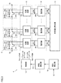
- FIG. 3 is a circuit block diagram showing a configuration of a portion related to control of the switch 2 in the control device 4 shown in FIG.
- the control device 4 includes a voltage detector 10, a power failure detector 11, a control unit 12, optical fibers FA1 to FAN, FB1 to FBN, an AC voltage generator 13, a DC voltage generator 14, and a driver 15. ..
- the voltage detector 10 detects the instantaneous value of the AC voltage VI supplied from the commercial AC power supply 5 (FIG. 1) and outputs a signal indicating the detected value.
- the power failure detector 11 determines whether or not the commercial AC power supply 5 is normal based on the output signal of the voltage detector 10, and outputs a signal PC indicating the determination result.
- the commercial AC power supply 5 When the AC input voltage VI is higher than the lower limit voltage, the commercial AC power supply 5 is determined to be normal, and the signal PC is set to the “H” level. When AC input voltage VI is lower than the lower limit voltage, it is determined that commercial AC power supply 5 is not normal, and signal PC is set to "L" level.
- the control unit 12 outputs optical signals ⁇ 1 to ⁇ N and ⁇ 1 to ⁇ N in response to the signal PC.
- the optical signals ⁇ 1 to ⁇ N are given to the driver 15 via the optical fibers FA1 to FAN, respectively, and the optical signals ⁇ 1 to ⁇ N are given to the driver 15 via the optical fibers FB1 to FBN, respectively.
- the driver 15 turns on the IGBT units U1 to UN in response to the optical signals ⁇ 1 to ⁇ N, and turns off the IGBT units U1 to UN in response to the optical signals ⁇ 1 to ⁇ N.
- the control unit 12 When the signal PC is at the "H” level, the control unit 12 outputs the optical signals ⁇ 1 to ⁇ N, stops the output of the optical signals ⁇ 1 to ⁇ N, and turns on the IGBT units U1 to UN.
- the control unit 12 stops the output of the optical signals ⁇ 1 to ⁇ n and outputs the optical signals ⁇ 1 to ⁇ n to turn off the IGBT units U1 to Un for a predetermined time. After the elapse of Td, the output of the optical signals ⁇ (n+1) to ⁇ N is stopped and the optical signals ⁇ (n+1) to ⁇ N are output to turn off the IGBT units U(n+1) to UN.
- the predetermined time Td is set to a time necessary and sufficient for turning off the IGBT units U1 to Un in the on state.
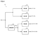
- FIG. 4 is a block diagram showing the configuration of the control unit 12 (FIG. 3).
- the control unit 12 includes a delay circuit 20 and light emitting units 22 to 25.
- the output signal PC of the power failure detector 11 is given to the light emitting units 22 and 24 and the delay circuit 20.
- the delay circuit 20 includes an even number (four stages in FIG. 5) of inverters 26 connected in series, and an OR gate 27.
- the signal PC is applied to one input node of the OR gate 27 through the even numbered inverters 26 and directly to the other input node of the OR gate 27.
- the output signal PC1 of the OR gate 27 is at the “H” level.
- the output signal ⁇ 26 of the final stage inverter 26 is at the "H” level.
- the signal ⁇ 26 goes to the “L” level and the signal PC1 falls to the “L” level after the delay time Td of the even-numbered inverters 26 elapses. Can be lowered.
- the signal PC1 is immediately raised to the "H” level.
- the delay circuit 20 passes the rising edge of the signal PC as it is and delays the falling edge of the signal PC by a predetermined time Td to generate the signal PC1.
- the output signal PC1 of the delay circuit 20 is given to the light emitting units 23 and 25.
- the light emitting unit 22 outputs the optical signals ⁇ 1 to ⁇ n when the signal PC is at “H” level, and stops the output of the optical signals ⁇ 1 to ⁇ n when the signal PC is at “L” level.
- the light emitting unit 23 outputs the optical signals ⁇ (n+1) to ⁇ N when the output signal PC1 of the delay circuit 20 is at the “H” level, and outputs the optical signal ⁇ ( when the signal PC1 is at the “L” level.
- the output of n + 1) to ⁇ N is stopped.
- the light emitting unit 24 outputs the optical signals ⁇ 1 to ⁇ n when the signal PC is at “L” level, and stops the output of the optical signals ⁇ 1 to ⁇ n when the signal PC is at “H” level.
- the light emitting unit 25 outputs the optical signals ⁇ (n+1) to ⁇ N when the output signal PC1 of the delay circuit 20 is at the “L” level, and outputs the optical signal ⁇ ( when the signal PC1 is at the “H” level.
- the output of n + 1) to ⁇ N is stopped.
- FIG. 6A shows the waveform of the output signal PC of the power failure detector 11 (FIG. 3)
- FIG. 6B shows the waveform of the output signal PC1 of the delay circuit 20 (FIG. 4).
- FIG. 6C shows the waveforms of the output signals ⁇ 1 to ⁇ n of the light emitting unit 22 (FIG. 4), and FIG. 6D shows the waveforms of the output signals ⁇ (n + 1) to ⁇ N of the light emitting unit 23 (FIG. 4).
- 6 (E) shows the waveforms of the output signals ⁇ 1 to ⁇ n of the light emitting unit 24 (FIG. 4), and FIG. 6 (F) shows the output signals ⁇ (n + 1) to ⁇ N of the light emitting unit 25 (FIG. 4). The waveform is shown.
- the AC voltage VI is normally supplied from the commercial AC power supply 5, and the signal PC is set to the “H” level.
- the optical signals ⁇ 1 to ⁇ N are output from the light emitting units 22 and 23, the output of the optical signals ⁇ 1 to ⁇ N from the light emitting units 24 and 25 is stopped, and the IGBT units U1 to UN are turned on.
- the signal PC is shut down from the "H” level to the "L” level, the output of the optical signals ⁇ 1 to ⁇ n is stopped from the light emitting unit 22, and the optical signal ⁇ 1 is stopped from the light emitting unit 24. To ⁇ n are output, and the IGBT units U1 to Un are turned off.
- both signals PC1 and PC2 fall from “H” level to “L” level.
- the output of the optical signals ⁇ (n + 1) to ⁇ N is stopped from the light emitting unit 23, the optical signals ⁇ (n + 1) to ⁇ N are output from the light emitting unit 25, and the IGBT units U (n + 1) to UN are turned off.
- both the signals PC and PC1 are raised from the “L” level to the “H” level.
- the light emitting units 22 and 23 output the optical signals ⁇ 1 to ⁇ N
- the light emitting units 24 and 25 stop the output of the optical signals ⁇ 1 to ⁇ N
- the IGBT units U1 to UN are turned on.
- the AC voltage generator 13 outputs N AC voltages VA1 to VAN.
- the magnitudes (for example, effective values) of the AC voltages VA1 to VAN are the same, for example, 200V.
- the DC voltage generator 14 converts the AC voltages VA1 to VAN into DC voltages VD1 to VDN, respectively.
- the DC voltages VD1 to VDN have the same magnitude.
- FIG. 7 is a circuit block diagram showing the configuration of the AC voltage generator 13 shown in FIG.
- the AC voltage generator 13 includes an AC power supply 28 and N isolation transformers T1 to TN.
- the AC power supply 28 generates an AC power supply voltage V0 having a predetermined frequency f0.
- the frequency f0 is set to a frequency (for example, 10 kHz) that can be transmitted by a relatively small isolation transformer.
- the AC output voltage VA0 of the AC power supply 28 is applied to the primary winding W1 of the isolation transformer T1, and the secondary windings W2 of the isolation transformers T1 to T (N-1) are the primary windings of the isolation transformers T2 to TN, respectively.
- AC voltages VA1 to VAN are output from the secondary windings W2 of the insulating transformers T1 to TN, which are connected to W1.
- the ratio of the number of turns of the secondary winding W2 to the number of turns of the primary winding W1 is 1 in each of the isolation transformers T0 to TN, and the transformation ratio of each of the isolation transformers T1 to T0 is 1. Therefore, the magnitudes of the AC power supply voltage VA0 and the AC voltages VA1 to VAN are the same.
- the DC voltage generator 14 includes N rectifiers R1 to RN.
- the rectifiers R1 to RN respectively receive the AC voltages VA1 to VAN and output the DC voltages VD1 to VDN, respectively.
- the rectifier R1 rectifies the AC voltage VA1 to generate the DC voltage VD1.
- Each of the other rectifiers R2 to RN is similar to the rectifier R1.
- the driver 15 includes N switching circuits S1 to SN.
- Switching circuits S1 to SN receive DC voltages VD1 to VDN, respectively, and are connected between the gates and emitters of IGBTs Q1 to QN, respectively.
- the switching circuits S1 to SN are connected to the control unit 12 via the optical fibers FA1 to FAN, respectively, and are connected to the control unit 12 via the optical fibers FB1 to FBN, respectively.
- the switching circuit S1 responds to the optical signal ⁇ 1 from the optical fiber FA1 and applies a DC voltage VD1 between the gate and the emitter of the IGBT Q1 to turn on the IGBT unit U1.
- the switching circuit S1 connects the gate and the emitter of the IGBTQ1 and turns off the IGBT unit U1 in response to the optical signal ⁇ 1 from the optical fiber FB1.
- Each of the other switching circuits S2 to SN is similar to switching circuit S1.
- the switch 2 (IGBT units U1 to UN) is turned on, and when the optical signals ⁇ 1 to ⁇ N are output from the control unit 12, the switch 2 (IGBT units U1 to UN) is turned on. UN) turns off.
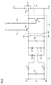
- FIG. 8 is a circuit diagram showing the configuration of the rectifier R1 and the switching circuit S1 shown in FIG.
- the rectifier R1 includes input terminals 30a and 30b, output terminals 30c and 30d, capacitors 31,38, resistance elements 32 and 33, and diodes 34 to 37
- the switching circuit S1 includes optical transistors 39 and 40. ..
- the input terminals 30a and 30b of the rectifier R1 receive the AC voltage VA1 from the secondary winding W2 of the corresponding isolation transformer T1.
- the capacitor 31 is called a matching capacitor and is connected between the input terminals 30a and 30b.
- the capacitance value of the capacitor 31 is set so that the AC output voltages VA1 to VAN of the insulating transformers T1 to TN are equal in magnitude.
- One terminals of the resistance elements 32 and 33 are connected to the input terminals 30a and 30b, respectively, and the other terminals thereof are connected to the anodes of the diodes 34 and 35, respectively.
- the resistance elements 32 and 33 adjust the input current of the rectifier R1.
- the cathodes of the diodes 34 and 35 are both connected to the output terminal 30c.
- the anodes of the diodes 36 and 37 are both connected to the output terminal 30d, and their cathodes are connected to the anodes of the diodes 34 and 35, respectively.
- the diodes 34 to 37 form a full-wave rectifier circuit and convert the AC voltage VA1 into the DC voltage VD1.
- Capacitor 38 smoothes and stabilizes DC voltage VD1.
- the collector of the optical transistor 39 is connected to the output terminal 30c of the rectifier R1, its emitter is connected to the gate of the IGBT Q1, and its base is connected to the output end of the optical fiber FA1.
- the optical transistor 39 is turned on when the optical signal ⁇ 1 is output from the control unit 12 (FIG. 3) (when the commercial AC power source 5 is healthy), and when the output of the optical signal ⁇ 1 is stopped (the commercial AC power source 5). Power off).
- the collector of the optical transistor 40 is connected to the gate of the IGBT Q1, its emitter is connected to the emitter of the IGBT Q1, and its base is connected to the output end of the optical fiber FB1.
- the optical transistor 40 is turned on when the optical signal ⁇ 1 is output from the control unit 12 (FIG. 2) (when the commercial AC power supply 5 is out of power), and when the output of the optical signal ⁇ 1 is stopped (the commercial AC power supply 5). Turn off the sound).
- the other rectifiers R2 to RN and the switching circuits S2 to SN are the same as the rectifier R1 and the switching circuit S1.
- the operation of the control device 4 shown in FIGS. 3 to 8 will be described.
- the instantaneous value of the AC voltage VI supplied from the commercial AC power source 5 is detected by the voltage detector 10, and based on the detection result, the power failure detector 11 outputs the AC voltage VI from the commercial AC power source 5. It is determined whether the supply is normal.
- the output signal PC of the power failure detector 11 is set to the “H” level.
- the output signal PC of the power failure detector 11 is set to the “L” level.
- the signal PC is directly applied to the light emitting units 22 and 24 and is also applied to the delay circuit 20.
- the delay circuit 20 delays the falling edge of the signal PC by Td for a predetermined time to generate the signal PC1.
- the signal PC1 is given to the light emitting units 23 and 25.
- the light emitting units 22 and 23 When the signal PC is set to the “H” level, the light emitting units 22 and 23 output the optical signals ⁇ 1 to ⁇ N, and the light emitting units 24 and 25 stop outputting the optical signals ⁇ 1 to ⁇ N.
- the signal PC When the signal PC is lowered from the "H” level to the "L” level, the output of the optical signals ⁇ 1 to ⁇ n from the light emitting unit 22 is stopped, and after a predetermined time Td, the optical signals ⁇ (n + 1) to the light emitting unit 23 are stopped. The output of ⁇ N is stopped.
- the light emitting units 24 output the optical signals ⁇ 1 to ⁇ n, and after a predetermined time Td, the light emitting unit 25 outputs the optical signals ⁇ (n + 1) to ⁇ N. It is output.
- an AC power supply voltage VA0 is generated by the AC power supply 28 and applied to the primary winding W1 of the insulating transformer T1.
- the isolation transformers T1 to TN are sequentially connected, and their secondary windings W2 output AC voltages VA1 to VAN, respectively.
- the AC output voltages VA1 to VAN of the isolation transformers T1 to TN are given to the rectifiers R1 to RN, respectively.
- the AC voltage VA1 is applied between the input terminals 30a and 30b of the rectifier R1 as shown in FIG.
- a DC voltage VD1 is generated between the terminals of the capacitor 38.
- the DC voltage VD1 is given to the switching circuit S1.
- the AC voltages VA2 to VAN are converted into DC voltages VD2 to VDN by the rectifiers R1 to RN and given to the switching circuits S2 to SN.
- the optical signals ⁇ 1 to ⁇ N are output from the control unit 12 (FIG. 4) and the output of the optical signals ⁇ 1 to ⁇ N is stopped, and in each of the switching circuits S1 to SN, The optical transistor 39 turns on and the optical transistor 40 turns off. Thereby, the DC voltages VD1 to VDN are applied between the gates and the emitters of the IGBTs Q1 to QN via the phototransistors 39 of the switching circuits S1 to SN, and the IGBT units U1 to UN (that is, the switch 2) are turned on.
- the control unit 12 stops the output of the optical signals ⁇ 1 to ⁇ n and outputs the optical signals ⁇ 1 to ⁇ n, and after a predetermined time Td, the optical signals ⁇ (n + 1) to ⁇ N The output is stopped and the optical signals ⁇ (n+1) to ⁇ N are output.
- the optical transistor 40 When the output of the optical signals ⁇ 1 to ⁇ n is stopped and the optical signals ⁇ 1 to ⁇ n are output, the optical transistor 40 is turned on and the optical transistor 39 is turned off in each of the switching circuits S1 to Sn. As a result, the gates and emitters of the IGBT Q1 to Qn are connected by the optical transistors 40 of the switching circuits S1 to Sn, and the IGBT units U1 to Un are turned off.
- the optical transistor 40 When the output of the optical signals ⁇ (n + 1) to ⁇ N is stopped after the predetermined time Td and the optical signals ⁇ (n + 1) to ⁇ N are output, the optical transistor 40 is turned on in each of the switching circuits S (n + 1) to SN. At the same time, the phototransistor 39 is turned off. As a result, the gates and emitters of the IGBT Q (n + 1) to QN are connected by the optical transistors 40 of the switching circuits S (n + 1) to SN, the IGBT units U (n + 1) to UN are turned off, and the switch 2 is completely turned off. ..
- the switch 2 when the switch 2 is turned off, the IGBT units U1 to Un are turned off and then the IGTB units U(n+1) to UN are turned off. Therefore, as compared with the case where the IGBT units U1 to UN are turned off at once, the surge voltage generated between the terminals of the switch 2 can be reduced, and the life of the surge absorber 1 can be extended. Further, since it is not necessary to wait until the alternating current flowing through the switch 2 reaches the zero point, the switch 2 can be turned off quickly.
- FIG. 9 is a circuit block diagram showing a main part of the uninterruptible power supply according to the second embodiment of the present invention, and is a diagram to be compared with FIG.
- the uninterruptible power supply device differs from the uninterruptible power supply device of the first embodiment in that the control unit 12 is replaced by the control unit 50.
- the control unit 50 is obtained by replacing the delay circuit 20 of the control unit 12 with a zero point detector 51 and an OR gate 52.
- the zero-point detector 51 is activated when the output signal PC of the power failure detector 11 (FIG. 3) is at “L” level, and the AC output current IO of the AC output current IO is output based on the output signal of the current detector CT (FIG. 1). A zero point is detected and a signal DT indicating the detection result is output. At the zero point of the AC output current IO, the instantaneous value of the AC output current IO becomes 0A.
- the signal DT When the signal PC is at “H” level, the signal DT is fixed at “H” level. When signal PC is at “L” level, signal DT is lowered from “H” level to “L” level in response to detection of the zero point of AC output current IO.
- the OR gate 52 outputs the ethics signal PC5 of the signals PC and DT to the light emitting units 23 and 25.
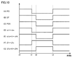
- FIG. 10A to 10G are time charts showing the operation of the control unit 50 shown in FIG.
- FIG. 10A shows the waveform of the output signal PC of the power failure detector 11 (FIG. 3)
- FIG. 10B shows the waveform of the output signal DT of the zero point detector 51 (FIG. 9)
- FIG. (C) shows the waveform of the output signal PC5 of the OR gate 52 (FIG. 9).
- FIG. 10 (D) shows the waveforms of the output signals ⁇ 1 to ⁇ n of the light emitting unit 22 (FIG. 8), and FIG. 10 (E) shows the waveforms of the output signals ⁇ (n + 1) to ⁇ N of the light emitting unit 23 (FIG. 8).
- 10 (F) shows the waveforms of the output signals ⁇ 1 to ⁇ n of the light emitting unit 24 (FIG. 8), and FIG. 10 (G) shows the output signals ⁇ (n + 1) to ⁇ N of the light emitting unit 25 (FIG. 8). The waveform is shown.
- the AC voltage VI is normally supplied from the commercial AC power supply 5
- the signal PC is set to the “H” level
- the output of the zero point detector 51 is output.
- the signal DT and the output signal PC5 of the OR gate 52 are both at "H” level.
- the optical signals ⁇ 1 to ⁇ N are output from the light emitting units 22 and 23
- the output of the optical signals ⁇ 1 to ⁇ N from the light emitting units 24 and 25 is stopped, and the IGBT units U1 to UN are turned on.
- the signal PC is shut down from the "H” level to the "L” level.
- the light emitting unit 22 stops outputting the optical signals ⁇ 1 to ⁇ n
- the light emitting unit 24 outputs the optical signals ⁇ 1 to ⁇ n
- the IGBT units U1 to Un are turned off.
- the light emitting unit 23 stops outputting the optical signals ⁇ (n+1) to ⁇ N, the light emitting unit 25 outputs the optical signals ⁇ (n+1) to ⁇ N, and the IGBT units U(n+1) to UN are turned off.
Landscapes
- Engineering & Computer Science (AREA)
- Power Engineering (AREA)
- Business, Economics & Management (AREA)
- Emergency Management (AREA)
- Power Conversion In General (AREA)
- Stand-By Power Supply Arrangements (AREA)
- Electronic Switches (AREA)
- Inverter Devices (AREA)
Abstract
Description
図1は、実施の形態1による無停電電源装置の構成を示す回路ブロック図である。この無停電電源装置は三相交流電力を負荷に供給するものであるが、図面および説明の簡単化のため、図1では一相に関連する部分のみが示されている。また、このような無停電電源装置は瞬低補償装置とも呼ばれる。
図9は、この発明の実施の形態2による無停電電源装置の要部を示す回路ブロック図であって、図4と対比される図である。図9を参照して、この無停電電源装置が実施の形態1の無停電電源装置と異なる点は、制御部12が制御部50で置換されている点である。制御部50は、制御部12の遅延回路20を零点検出器51およびORゲート52で置換したものである。
Claims (10)
- 第1および第2の端子間に直列接続され、第1および第2のグループに分割された複数のスイッチング素子を含むスイッチと、
前記スイッチをオンさせる場合には、前記複数のスイッチング素子をオンさせ、前記スイッチをオフさせる場合には、前記第1のグループのスイッチング素子をオフさせた後に前記第2のグループのスイッチング素子をオフさせる制御装置とを備える、電源装置。 - 前記第1のグループに属するスイッチング素子の耐圧の総和が前記第1および第2の端子間に発生する電圧よりも大きくなるように、前記第1のグループのスイッチング素子の数が設定されている、請求項1に記載の電源装置。
- 前記スイッチは、さらに、各スイッチング素子に対応して設けられて対応するスイッチング素子に並列接続され、対応するスイッチング素子をサージ電圧から保護するスナバ回路を含む、請求項1に記載の電源装置。
- 前記スナバ回路は、その抵抗値がその端子間電圧に応じて変化する抵抗器を含み、
前記スイッチがオフされている場合に前記抵抗器に流れる電流が予め定められた基準電流以下になるように、前記スナバ回路の数が設定されている、請求項3に記載の電源装置。 - 前記複数のスイッチング素子の各々はトランジスタであり、
前記スイッチは、さらに、それぞれ複数の前記トランジスタに逆並列に接続された複数のダイオードを含む、請求項1に記載の電源装置。 - さらに、前記第1の端子に接続され、前記電源装置をサージ電圧から保護するサージ吸収器を備える、請求項1に記載の電源装置。
- 各スイッチング素子をオフさせると当該スイッチング素子の電極間にサージ電圧が発生し、
前記第1の端子に発生するサージ電圧の大きさに応じて前記サージ吸収器の寿命が短くなり、
前記第1のグループのスイッチング素子をオフさせた後に前記第2のグループのスイッチング素子をオフさせることにより、前記第1の端子に発生するサージ電圧を低減する、請求項6に記載の電源装置。 - 前記制御装置は、前記スイッチをオフさせる場合には、前記第1のグループのスイッチング素子をオフさせてから予め定められた時間が経過した後に前記第2のグループのスイッチング素子をオフさせる、請求項1に記載の電源装置。
- 前記第1の端子は、交流電源から供給される交流電力を受け、
前記第2の端子は、交流電力によって駆動される負荷に接続され、
前記電源装置は、さらに、前記電源装置から前記負荷に流れる交流電流の瞬時値を検出する電流検出器を備え、
前記制御装置は、前記スイッチをオフさせる場合には、前記第1のグループのスイッチング素子をオフさせた後、前記電流検出器の検出値が0Aになるときに前記第2のグループのスイッチング素子をオフさせる、請求項1に記載の電源装置。 - 前記第1の端子は、交流電源から供給される交流電力を受け、
前記第2の端子は、交流電力によって駆動される負荷に接続され、
前記制御装置は、前記交流電源から交流電圧が正常に供給されている第1の場合には前記スイッチをオンさせ、前記交流電源から交流電圧が正常に供給されていない第2の場合には前記スイッチをオフさせ、
前記電源装置は、さらに、前記第2の端子に接続され、前記第1の場合には、前記交流電源から前記スイッチを介して供給される交流電力を直流電力に変換して電力貯蔵装置に蓄え、前記第2の場合には、前記電力貯蔵装置の直流電力を交流電力に変換して前記負荷に供給する双方向コンバータを備える、請求項1に記載の電源装置。
Priority Applications (5)
| Application Number | Priority Date | Filing Date | Title |
|---|---|---|---|
| PCT/JP2019/008534 WO2020178969A1 (ja) | 2019-03-05 | 2019-03-05 | 電源装置 |
| US17/052,711 US11290001B2 (en) | 2019-03-05 | 2019-03-05 | Power supply device |
| JP2019538280A JP6864103B2 (ja) | 2019-03-05 | 2019-03-05 | 電源装置 |
| CN201980040918.XA CN112335162B (zh) | 2019-03-05 | 2019-03-05 | 电源装置 |
| KR1020217000517A KR102547464B1 (ko) | 2019-03-05 | 2019-03-05 | 전원 장치 |
Applications Claiming Priority (1)
| Application Number | Priority Date | Filing Date | Title |
|---|---|---|---|
| PCT/JP2019/008534 WO2020178969A1 (ja) | 2019-03-05 | 2019-03-05 | 電源装置 |
Publications (1)
| Publication Number | Publication Date |
|---|---|
| WO2020178969A1 true WO2020178969A1 (ja) | 2020-09-10 |
Family
ID=72338457
Family Applications (1)
| Application Number | Title | Priority Date | Filing Date |
|---|---|---|---|
| PCT/JP2019/008534 Ceased WO2020178969A1 (ja) | 2019-03-05 | 2019-03-05 | 電源装置 |
Country Status (5)
| Country | Link |
|---|---|
| US (1) | US11290001B2 (ja) |
| JP (1) | JP6864103B2 (ja) |
| KR (1) | KR102547464B1 (ja) |
| CN (1) | CN112335162B (ja) |
| WO (1) | WO2020178969A1 (ja) |
Cited By (5)
| Publication number | Priority date | Publication date | Assignee | Title |
|---|---|---|---|---|
| JP2022098242A (ja) * | 2020-12-21 | 2022-07-01 | パナソニックIpマネジメント株式会社 | 電力変換装置 |
| JP7171946B1 (ja) * | 2021-06-02 | 2022-11-15 | 東芝三菱電機産業システム株式会社 | 電源装置 |
| WO2023233540A1 (ja) * | 2022-05-31 | 2023-12-07 | 東芝三菱電機産業システム株式会社 | 無停電電源装置 |
| WO2024075236A1 (ja) * | 2022-10-06 | 2024-04-11 | 東芝三菱電機産業システム株式会社 | 電源装置 |
| KR102955183B1 (ko) | 2022-05-31 | 2026-04-20 | 가부시키가이샤 티마이크 | 무정전 전원 장치 |
Families Citing this family (9)
| Publication number | Priority date | Publication date | Assignee | Title |
|---|---|---|---|---|
| WO2020105135A1 (ja) * | 2018-11-21 | 2020-05-28 | 東芝三菱電機産業システム株式会社 | 電源装置 |
| JP6666527B1 (ja) * | 2019-03-06 | 2020-03-13 | 東芝三菱電機産業システム株式会社 | 制御装置 |
| US11329642B1 (en) | 2021-03-15 | 2022-05-10 | Psemi Corporation | Bypass circuitry to improve switching speed |
| US11405034B1 (en) | 2021-05-14 | 2022-08-02 | Psemi Corporation | Body resistor bypass for RF FET switch stack |
| US11405031B1 (en) * | 2021-08-16 | 2022-08-02 | Psemi Corporation | Gate resistor bypass for RF FET switch stack |
| US11632107B1 (en) | 2021-10-01 | 2023-04-18 | Psemi Corporation | Gate resistive ladder bypass for RF FET switch stack |
| US11671135B2 (en) | 2021-10-01 | 2023-06-06 | Psemi Corporation | Methods and apparatus for reducing switching time of RF FET switching devices |
| TWI799046B (zh) * | 2021-12-30 | 2023-04-11 | 群光電能科技股份有限公司 | 智慧穩定供電系統 |
| KR102804007B1 (ko) * | 2022-06-27 | 2025-05-09 | 한국수자원공사 | 순시 재폐로에 의해 서지 유입을 방지하는 서지 보호기 |
Citations (4)
| Publication number | Priority date | Publication date | Assignee | Title |
|---|---|---|---|---|
| JPS63194543U (ja) * | 1987-05-29 | 1988-12-14 | ||
| JPH06104712A (ja) * | 1992-09-18 | 1994-04-15 | Hitachi Ltd | 半導体スイッチ |
| JP2000092817A (ja) * | 1998-09-16 | 2000-03-31 | Toshiba Corp | スナバ装置及び電力変換装置 |
| JP2017060317A (ja) * | 2015-09-17 | 2017-03-23 | 住友電気工業株式会社 | 電源装置及びそのスイッチ制御方法 |
Family Cites Families (19)
| Publication number | Priority date | Publication date | Assignee | Title |
|---|---|---|---|---|
| JPH02130901A (ja) * | 1988-11-11 | 1990-05-18 | Matsushita Electric Ind Co Ltd | サージ吸収器の保護装置 |
| JP2536919B2 (ja) | 1989-03-03 | 1996-09-25 | 富士電機株式会社 | 交流スイッチの電流零点遮断制御回路 |
| JPH06112791A (ja) * | 1992-09-28 | 1994-04-22 | Meidensha Corp | 半導体スイッチ回路 |
| JPH06244694A (ja) * | 1993-02-16 | 1994-09-02 | Yokogawa Electric Corp | 半導体スイッチ装置 |
| JPH11178321A (ja) * | 1997-12-12 | 1999-07-02 | Hitachi Ltd | 半導体電力変換装置 |
| JP2000049581A (ja) * | 1998-07-27 | 2000-02-18 | Hitachi Ltd | 半導体電力変換装置 |
| JP4700460B2 (ja) | 2005-09-27 | 2011-06-15 | 東芝三菱電機産業システム株式会社 | 直列半導体スイッチ装置 |
| JP4669860B2 (ja) * | 2007-07-06 | 2011-04-13 | 三菱電機株式会社 | 無停電電源装置 |
| US7508096B1 (en) * | 2007-09-20 | 2009-03-24 | General Electric Company | Switching circuit apparatus having a series conduction path for servicing a load and switching method |
| CN102948075B (zh) * | 2010-06-23 | 2021-01-26 | Abb瑞士股份有限公司 | 用于转换电压的方法和电压转换装置 |
| JP2012115039A (ja) * | 2010-11-24 | 2012-06-14 | Rohm Co Ltd | スイッチング電源の制御回路ならびにそれを用いたスイッチング電源および電子機器 |
| JP5851928B2 (ja) * | 2012-05-07 | 2016-02-03 | 株式会社Nttファシリティーズ | 半導体スイッチ及び半導体スイッチの制御方法 |
| JP2014147189A (ja) * | 2013-01-28 | 2014-08-14 | Fuji Electric Co Ltd | 電力変換装置の駆動回路 |
| US20160142050A1 (en) * | 2013-08-01 | 2016-05-19 | Sharp Kabushiki Kaisha | Multiple-unit semiconductor device and method for controlling the same |
| GB2545445A (en) * | 2015-12-16 | 2017-06-21 | General Electric Technology Gmbh | Voltage balancing of voltage source converters |
| WO2018220777A1 (ja) * | 2017-06-01 | 2018-12-06 | 東芝三菱電機産業システム株式会社 | 電源装置およびそれを用いた電源システム |
| DE102018211896B9 (de) * | 2018-07-17 | 2020-12-31 | Infineon Technologies Ag | HF-Schalter |
| WO2020105135A1 (ja) * | 2018-11-21 | 2020-05-28 | 東芝三菱電機産業システム株式会社 | 電源装置 |
| JP6666527B1 (ja) * | 2019-03-06 | 2020-03-13 | 東芝三菱電機産業システム株式会社 | 制御装置 |
-
2019
- 2019-03-05 US US17/052,711 patent/US11290001B2/en active Active
- 2019-03-05 WO PCT/JP2019/008534 patent/WO2020178969A1/ja not_active Ceased
- 2019-03-05 CN CN201980040918.XA patent/CN112335162B/zh active Active
- 2019-03-05 JP JP2019538280A patent/JP6864103B2/ja active Active
- 2019-03-05 KR KR1020217000517A patent/KR102547464B1/ko active Active
Patent Citations (4)
| Publication number | Priority date | Publication date | Assignee | Title |
|---|---|---|---|---|
| JPS63194543U (ja) * | 1987-05-29 | 1988-12-14 | ||
| JPH06104712A (ja) * | 1992-09-18 | 1994-04-15 | Hitachi Ltd | 半導体スイッチ |
| JP2000092817A (ja) * | 1998-09-16 | 2000-03-31 | Toshiba Corp | スナバ装置及び電力変換装置 |
| JP2017060317A (ja) * | 2015-09-17 | 2017-03-23 | 住友電気工業株式会社 | 電源装置及びそのスイッチ制御方法 |
Cited By (11)
| Publication number | Priority date | Publication date | Assignee | Title |
|---|---|---|---|---|
| JP2022098242A (ja) * | 2020-12-21 | 2022-07-01 | パナソニックIpマネジメント株式会社 | 電力変換装置 |
| JP7599146B2 (ja) | 2020-12-21 | 2024-12-13 | パナソニックIpマネジメント株式会社 | 電力変換装置 |
| JP7171946B1 (ja) * | 2021-06-02 | 2022-11-15 | 東芝三菱電機産業システム株式会社 | 電源装置 |
| WO2022254627A1 (ja) * | 2021-06-02 | 2022-12-08 | 東芝三菱電機産業システム株式会社 | 電源装置 |
| WO2023233540A1 (ja) * | 2022-05-31 | 2023-12-07 | 東芝三菱電機産業システム株式会社 | 無停電電源装置 |
| JP7400124B1 (ja) * | 2022-05-31 | 2023-12-18 | 東芝三菱電機産業システム株式会社 | 無停電電源装置 |
| US20240339862A1 (en) * | 2022-05-31 | 2024-10-10 | Toshiba Mitsubishi-Electric Industrial Systems Corporation | Uninterruptible power supply apparatus |
| US12334774B2 (en) * | 2022-05-31 | 2025-06-17 | Tmeic Corporation | Uninterruptible power supply apparatus |
| KR102955183B1 (ko) | 2022-05-31 | 2026-04-20 | 가부시키가이샤 티마이크 | 무정전 전원 장치 |
| WO2024075236A1 (ja) * | 2022-10-06 | 2024-04-11 | 東芝三菱電機産業システム株式会社 | 電源装置 |
| JP7477941B1 (ja) * | 2022-10-06 | 2024-05-02 | 株式会社Tmeic | 電源装置 |
Also Published As
| Publication number | Publication date |
|---|---|
| KR20210018466A (ko) | 2021-02-17 |
| JPWO2020178969A1 (ja) | 2021-03-11 |
| CN112335162A (zh) | 2021-02-05 |
| US20210242770A1 (en) | 2021-08-05 |
| KR102547464B1 (ko) | 2023-06-23 |
| CN112335162B (zh) | 2024-08-30 |
| US11290001B2 (en) | 2022-03-29 |
| JP6864103B2 (ja) | 2021-04-21 |
Similar Documents
| Publication | Publication Date | Title |
|---|---|---|
| JP6864103B2 (ja) | 電源装置 | |
| US11101740B2 (en) | Modular power supply system | |
| US11139749B2 (en) | Semiconductor device | |
| US8848322B2 (en) | Gate control circuit, power module and associated method | |
| JP6342063B2 (ja) | 電力変換装置 | |
| AU2011362347B2 (en) | Gate control circuit, power module and associated method | |
| WO2019038830A1 (ja) | 電源装置 | |
| EP3813239A1 (en) | Self-feeding circuit and power conversion device | |
| US10951131B2 (en) | Converter and method for driving converter | |
| US11196292B2 (en) | Uninterruptible power supply system | |
| US11233420B2 (en) | Uninterruptible power supply apparatus | |
| JP6666527B1 (ja) | 制御装置 | |
| JPWO2018043226A1 (ja) | スイッチング電源装置および半導体装置 | |
| WO2019155522A1 (ja) | 電力変換装置 | |
| CN113544954B (zh) | 电力变换装置 | |
| JP2019187005A (ja) | 電力変換装置 | |
| JP7108130B1 (ja) | 無停電電源装置 | |
| JP7551043B1 (ja) | 電力変換装置 | |
| JP7271767B1 (ja) | 同期発電機用の自動電圧調整装置 | |
| KR20180101857A (ko) | 전력 변환 장치 및 이를 포함하는 공기 조화기 |
Legal Events
| Date | Code | Title | Description |
|---|---|---|---|
| ENP | Entry into the national phase |
Ref document number: 2019538280 Country of ref document: JP Kind code of ref document: A |
|
| 121 | Ep: the epo has been informed by wipo that ep was designated in this application |
Ref document number: 19917939 Country of ref document: EP Kind code of ref document: A1 |
|
| ENP | Entry into the national phase |
Ref document number: 20217000517 Country of ref document: KR Kind code of ref document: A |
|
| NENP | Non-entry into the national phase |
Ref country code: DE |
|
| 122 | Ep: pct application non-entry in european phase |
Ref document number: 19917939 Country of ref document: EP Kind code of ref document: A1 |