WO2020158130A1 - 半導体装置 - Google Patents
半導体装置 Download PDFInfo
- Publication number
- WO2020158130A1 WO2020158130A1 PCT/JP2019/046004 JP2019046004W WO2020158130A1 WO 2020158130 A1 WO2020158130 A1 WO 2020158130A1 JP 2019046004 W JP2019046004 W JP 2019046004W WO 2020158130 A1 WO2020158130 A1 WO 2020158130A1
- Authority
- WO
- WIPO (PCT)
- Prior art keywords
- substrate
- solid
- semiconductor device
- exposed
- state imaging
- Prior art date
- Legal status (The legal status is an assumption and is not a legal conclusion. Google has not performed a legal analysis and makes no representation as to the accuracy of the status listed.)
- Ceased
Links
Images







Classifications
-
- H—ELECTRICITY
- H10—SEMICONDUCTOR DEVICES; ELECTRIC SOLID-STATE DEVICES NOT OTHERWISE PROVIDED FOR
- H10F—INORGANIC SEMICONDUCTOR DEVICES SENSITIVE TO INFRARED RADIATION, LIGHT, ELECTROMAGNETIC RADIATION OF SHORTER WAVELENGTH OR CORPUSCULAR RADIATION
- H10F39/00—Integrated devices, or assemblies of multiple devices, comprising at least one element covered by group H10F30/00, e.g. radiation detectors comprising photodiode arrays
- H10F39/80—Constructional details of image sensors
- H10F39/804—Containers or encapsulations
-
- H—ELECTRICITY
- H10—SEMICONDUCTOR DEVICES; ELECTRIC SOLID-STATE DEVICES NOT OTHERWISE PROVIDED FOR
- H10F—INORGANIC SEMICONDUCTOR DEVICES SENSITIVE TO INFRARED RADIATION, LIGHT, ELECTROMAGNETIC RADIATION OF SHORTER WAVELENGTH OR CORPUSCULAR RADIATION
- H10F39/00—Integrated devices, or assemblies of multiple devices, comprising at least one element covered by group H10F30/00, e.g. radiation detectors comprising photodiode arrays
- H10F39/80—Constructional details of image sensors
- H10F39/809—Constructional details of image sensors of hybrid image sensors
-
- H—ELECTRICITY
- H10—SEMICONDUCTOR DEVICES; ELECTRIC SOLID-STATE DEVICES NOT OTHERWISE PROVIDED FOR
- H10F—INORGANIC SEMICONDUCTOR DEVICES SENSITIVE TO INFRARED RADIATION, LIGHT, ELECTROMAGNETIC RADIATION OF SHORTER WAVELENGTH OR CORPUSCULAR RADIATION
- H10F77/00—Constructional details of devices covered by this subclass
- H10F77/60—Arrangements for cooling, heating, ventilating or compensating for temperature fluctuations
-
- H—ELECTRICITY
- H10—SEMICONDUCTOR DEVICES; ELECTRIC SOLID-STATE DEVICES NOT OTHERWISE PROVIDED FOR
- H10W—GENERIC PACKAGES, INTERCONNECTIONS, CONNECTORS OR OTHER CONSTRUCTIONAL DETAILS OF DEVICES COVERED BY CLASS H10
- H10W40/00—Arrangements for thermal protection or thermal control
- H10W40/10—Arrangements for heating
-
- H—ELECTRICITY
- H10—SEMICONDUCTOR DEVICES; ELECTRIC SOLID-STATE DEVICES NOT OTHERWISE PROVIDED FOR
- H10W—GENERIC PACKAGES, INTERCONNECTIONS, CONNECTORS OR OTHER CONSTRUCTIONAL DETAILS OF DEVICES COVERED BY CLASS H10
- H10W70/00—Package substrates; Interposers; Redistribution layers [RDL]
- H10W70/60—Insulating or insulated package substrates; Interposers; Redistribution layers
Definitions
- the present technology relates to semiconductor devices. Specifically, it relates to a semiconductor device in which a solid-state image sensor is mounted on a substrate.
- a semiconductor package has been proposed in which a heat generating portion of a semiconductor chip is locally exposed and then cooled by contacting a heat sink member (for example, refer to Patent Document 1).
- a semiconductor device has been proposed in which a housing of a semiconductor chip and a heat radiation fin are bonded with a heat conductive grease (for example, refer to Patent Document 2).
- the heat generated during the operation of the semiconductor chip is exhausted by providing the cooling member on the surface of the semiconductor chip, that is, the surface opposite to the surface facing the substrate.
- the semiconductor chip is a solid-state image sensor
- the temperature distribution in the solid-state image sensor varies due to heat generation, the image quality of the captured image may be locally deteriorated.
- the present technology was created in view of such circumstances, and its purpose is to efficiently discharge heat without impairing the imaging characteristics of the solid-state imaging device.
- the present technology has been made in order to solve the above-mentioned problems, and the first side surface thereof includes a substrate provided with metal wiring, a solid-state imaging device mounted on the surface of the substrate, and a predetermined heat source.
- a semiconductor device comprising: an adhesive portion having electrical conductivity and adhering a predetermined region on one surface of the solid-state imaging device to the substrate. This brings about the effect that the heat generated in the solid-state imaging device is discharged to the metal wiring of the substrate via the adhesive portion.
- the adhesive portion may have a larger area in the high temperature portion than in the low temperature portion, depending on the temperature distribution of the solid-state imaging device. This brings about the effect of exhausting heat in an area corresponding to the temperature distribution.
- the substrate includes an insulating film on the surface
- the insulating film on the substrate includes an exposed portion that opens in the predetermined region to expose the metal wiring
- the part may adhere the predetermined region of the solid-state image sensor and the metal wiring of the substrate.
- the exposed portion has an effect of adhering the adhesive portion to the metal wiring of the substrate to exhaust heat.
- the exposed portion may be arranged in a higher temperature portion more than in a lower temperature portion in accordance with the temperature distribution of the solid-state imaging device. This brings about the effect of exhausting heat through the number of exposed portions corresponding to the temperature distribution.
- the exposed portions may be arranged at a higher density in the high temperature portion than in the low temperature portion, depending on the temperature distribution of the solid-state imaging device. This brings about the effect of exhausting heat through the exposed portion having a density corresponding to the temperature distribution.
- the exposed portion may have a plurality of circular shapes. It may also have other shapes such as elliptical or angular shapes.
- the predetermined region may be a region where the solid-state imaging device has a maximum temperature during operation. This brings about an effect that heat is exhausted toward the metal wiring of the substrate via the adhesive portion in the region set according to the maximum temperature during operation of the solid-state imaging device.
- the predetermined area may be an area occupied by a predetermined circuit in the solid-state imaging device. This brings about an effect that heat is exhausted toward the metal wiring of the substrate through the adhesive in the area occupied by the predetermined circuit.
- the predetermined circuit may be, for example, an analog-digital conversion circuit or a predetermined logic circuit.
- the adhesive section may include a plurality of types of adhesives having different thermoconductivity according to the temperature distribution of the solid-state imaging device. This brings about the effect of adjusting the heat dissipation according to the temperature distribution.
- FIG. 4 is a top view for explaining a structural example of the substrate 100 according to the first embodiment of the present technology. It is a figure showing an example of a process of mounting element 200 in a 1st embodiment of this art on substrate 100. It is a figure showing an example of a manufacturing process of a semiconductor device containing substrate 100 and element 200 in a 1st embodiment of this art. It is a figure showing an example of heat dissipation in a 1st embodiment of this art.
- FIG. 1 shows an example of the solid-state image sensor of the laminated structure in 2nd Embodiment of this technique. It is a top view for explaining the constructional example of substrate 100 in a 2nd embodiment of this art. It is a figure showing the 1st modification of exposed part 110 in an embodiment of this art. It is a figure showing the 2nd modification of exposed part 110 in an embodiment of this art. It is a figure showing the 3rd modification of exposed part 110 in an embodiment of this art. It is a figure showing the 4th modification of exposed part 110 in an embodiment of this art. It is a figure showing the 5th modification of exposed part 110 in an embodiment of this art. It is a figure showing the 6th modification of exposed part 110 in an embodiment of this art.
- First embodiment an example of a solid-state imaging device in which pixels and circuits are formed on the same silicon substrate
- Second embodiment an example of a solid-state image sensor having a laminated structure
- FIG. 1 is a sectional view showing an example of a structure of a semiconductor device according to an embodiment of the present technology.
- the element 200 is mounted on the surface of a base silicon substrate 100.
- the element 200 is a semiconductor chip, and a solid-state image pickup element is assumed in the following embodiments. That is, the device 200 is an example of the solid-state imaging device described in the claims.
- a predetermined area on the surface of the element 200 mounted on the substrate 100 is selectively bonded to the substrate 100 via the bonding portion 190.
- the predetermined region is a region directly below the heat generating portion 201 of the element 200, which is called a hot spot (local high temperature portion).
- a hot spot local high temperature portion.
- it is designed so as not to exceed the heat-resistant guaranteed temperature, so it is difficult to assume that extremely high heat will be generated even in a hot spot.
- a part of the element 200 reaches a temperature close to the guaranteed heat resistance (for example, about 60° C.).
- the substrate 100 is a substrate that serves as a base of a semiconductor device, and a printed circuit board is assumed, for example.
- a solder resist is formed on the surface of the substrate 100 as an insulating film for protection. Then, on the substrate 100 on which the element 200 is mounted, a solder resist is preliminarily opened at a position corresponding to a position directly below the heat generating portion 201 of the element 200. As a result, the metal wiring of the substrate 100 is exposed.
- Adhesive part 190 is applied to the part of the substrate 100 where the metal wiring is exposed.
- the adhesive section 190 is an adhesive having a predetermined thermal conductivity.
- the area directly below the heat generating portion 201 of the element 200 is bonded to the exposed portion of the metal wiring of the substrate 100 via the bonding portion 190. As a result, the heat of the heat generating portion 201 is exhausted toward the metal wiring.
- the input/output terminals of the element 200 are arranged on the peripheral portion of the upper surface, and are electrically connected to the substrate 100 by wire bonding via the wire 300.
- the wire 300 for example, a gold wire is assumed.
- a frame body 400 is provided around the element 200 on the substrate 100.
- a transparent material 500 such as glass is provided on the upper portion of the frame 400.
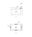
- FIG. 2 is a diagram showing an example of the temperature distribution of the element 200 according to the first embodiment of the present technology.
- a pixel portion 210 serving as a light receiving surface is formed in a substantially central portion of the surface, and the other circuit portion 220 is formed around the pixel portion 210.
- the circuit unit 220 for example, a signal processing circuit such as an AD (Analog-to-Digital) conversion circuit is assumed. That is, the circuit unit 220 is an example of the analog-digital conversion circuit described in the claims. However, this is an example, and other logic circuits may be applicable.
- the circuit section 220 When driving the element 200 as the solid-state image sensor, the circuit section 220 mainly generates heat. However, the amount of heat generation varies depending on the function of the circuit, and for example, as shown in b in the figure, a normal heat generating portion 221 and a high heat generating portion 222 higher than that may occur. When the influence of these heats affects the neighboring pixel portion 210, there is a possibility that image quality deterioration such as increase of noise may occur.
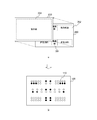
- FIG. 3 is a top view for explaining a structural example of the substrate 100 according to the first embodiment of the present technology.
- the circuit portion 220 around the pixel portion 210 serves as a main heat source as shown in a in the figure. Therefore, as shown by b in the figure, a circular or dot-shaped opening of the solder resist is provided in advance on the substrate 100 at a position directly below the heat generating portions 221 and 222 of the element 200, and It functions as the exposed portion 110 where the metal wiring is exposed.
- the exposed portions 110 be provided with openings at a density higher than that directly below the heat generating portion 221 immediately below the high heat generating portion 222.
- the shape of the opening of the exposed portion 110 is formed of a plurality of circular shapes is shown, but it may have an ellipse or a rectangular shape other than this.
- FIG. 4 is a diagram showing an example of a process of mounting the element 200 on the substrate 100 in the first embodiment of the present technology.
- the substrate 100 at a position directly below the heat generating portions 221 and 222 of the element 200 is provided with an exposed portion 110 where the solder resist is opened and the metal wiring is exposed.
- the element 200 is mounted on the surface of the substrate 100 as shown in b in the figure.
- the adhesive portion 190 is applied to the exposed portion 110 of the substrate 100, as shown in the sectional view of FIG.
- the exposed portion 110 of the substrate 100 and the heat generating portions 221 and 222 of the element 200 are bonded together via the bonding portion 190.
- FIG. 5 is a diagram showing an example of a manufacturing process of a semiconductor device including the substrate 100 and the element 200 according to the first embodiment of the present technology.
- wire bonding is performed with a wire 300 in order to electrically connect the input/output terminal arranged on the peripheral portion of the upper surface of the element 200 and the substrate 100.
- the frame body 400 is bonded to the substrate 100 in the peripheral portion of the element 200. Further, as shown by c in the figure, the transparent material 500 is adhered to the upper portion of the frame body 400. As a result, a semiconductor device is formed.
- FIG. 6 is a diagram showing an example of heat dissipation in the first embodiment of the present technology.
- the structure is such that heat is easily radiated through the metal wiring 150 in the substrate 100. ing.
- the exposed portion 110 where the metal wiring is exposed is provided on the substrate 100 at a position immediately below the heat generating portions 221 and 222 of the element 200, and the exposed portion 110 through which the metal wiring is exposed is provided via the adhesive portion 190. Selectively bond. Thereby, the heat generated in the element 200 can be radiated from the metal wiring 150 in the substrate 100.
- Second Embodiment> In the above-described first embodiment, the case where the solid-state image sensor is formed on the same silicon substrate is assumed, but in recent years, a solid-state image sensor having a laminated structure has been used. Therefore, in the second embodiment, an example assuming a solid-state imaging device having a laminated structure will be described.
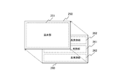
- FIG. 7 is a figure which shows an example of the solid-state image sensor of the laminated structure in 2nd Embodiment of this technique.
- the laminated solid-state imaging device has, for example, a structure in which a layer 250 having a pixel portion 251 serving as a light-receiving surface and a layer 260 having a signal processing circuit portion for AD conversion or the like are laminated.
- the circuit section when driven as a solid-state image sensor, the circuit section mainly generates heat.
- a heat generating portion 261 of a normal degree and a high heat generating portion 262 higher than that may occur.
- image quality deterioration such as increase of noise may occur.
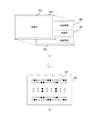
- FIG. 8 is a top view for explaining a structural example of the substrate 100 according to the second embodiment of the present technology.
- the substrate 100 is provided with an opening of a solder resist in a position immediately below the heat generating portions 261 and 262 in advance so that the metal wiring of the substrate 100 is exposed as an exposed portion 110. Make it work.
- the solid-state imaging device having the laminated structure including the layers 250 and 260 is mounted on the substrate 100.
- the adhesive portion 190 having thermal conductivity is applied to the exposed portion 110 of the substrate 100 to adhere the element.
- the portion directly below the heat generating portions 261 and 262 of the element is bonded to the substrate 100 by the bonding portion 190.
- the heat generated by the element has an in-plane distribution
- a larger amount of metal wiring is exposed on the substrate 100 at a position directly below the high heat generating section 262 and heat is radiated through the adhesive section 190, so that the in-plane temperature is increased.
- the distribution can be reduced to make it uniform. It is also possible to adjust the number and area of the exposed portions 110 of the metal wiring according to the heat generation level of the element.
- the exposed portion 110 in which the metal wiring is exposed is provided on the substrate 100 at a position immediately below the heat generating portions 261 and 262 of the element having the laminated structure, and the adhesive portion 190 is interposed therebetween. And glue them together.
- the heat generated in the element having the laminated structure can be radiated from the metal wiring 150 in the substrate 100.
- the solder resist of the substrate 100 is opened in a circular shape or a dot shape to expose the metal wiring 150 to the exposed portion 110.
- a large number of openings are provided immediately below the high heat generation portion and a small number of openings are provided in the low heat generation portion to promote heat dissipation from the high heat generation portion and make the temperature distribution in the element surface uniform.
- various modifications of the opening shape and arrangement of the exposed portion 110 are assumed as follows.
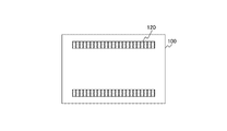
- FIG. 9 is a figure which shows the 1st modification of the exposed part 110 in embodiment of this technique.
- the exposed portion 120 is exposed. That is, the opening shape of the exposed portion 120 is rectangular. In this case, the exposed portion 120 may be coated with a large number of adhesive portions 190 in a linear shape to adhere the element.
- the arrangement of the exposed portion 120 can be applied when there are few restrictions on the wiring on the substrate 100.
- FIG. 10 is a diagram showing a second modified example of the exposed part 110 in the embodiment of the present technology.
- the exposed portions 120 are not provided on both sides of the substrate 100.
- the element 190 may be adhered by applying the adhesive portion 190 thereon. Thereby, the heat dissipation can be adjusted.
- FIG. 11 is a diagram illustrating a third modified example of the exposed portion 110 according to the embodiment of the present technology.
- the density of the exposed portion 110 immediately below them may be changed according to the temperature distribution.
- FIG. 12 is a diagram illustrating a fourth modified example of the exposed portion 110 according to the embodiment of the present technology.
- the exposed portion 110 may be arranged according to the change.
- FIG. 13 is a diagram showing a fifth modified example of the exposed portion 110 according to the embodiment of the present technology.
- the high heat generation portion 202 which is assumed to generate a large amount of heat, as shown in a in FIG. It is desirable to improve the heat dissipation by directly adhering the metal to the metal wiring 150.
- the exposed portion 110 is reduced in number and is connected by the adhesive portion 192 to improve heat dissipation. It may be suppressed. As a result, the heat dissipation can be adjusted to make the temperature distribution in the element plane uniform.
- the low heat generation portion 204 which is assumed to have a low heat generation amount, as shown in c in the figure, the solder resist of the substrate 100 is not opened, and the metal wiring 150 of the substrate 100 is not exposed to the adhesive portion. Bonded by 193. Thereby, the heat dissipation can be further suppressed and the temperature distribution in the element surface can be made more uniform.
- FIG. 14 is a diagram showing a sixth modified example of the exposed portion 110 according to the embodiment of the present technology.
- an adhesive portion 192 where the metal wiring 150 is exposed and an adhesive portion 193 where the metal wiring 150 is not exposed are mixed.
- the adhesive portions 192 and 193 may be provided in combination as shown in FIG. Thereby, the heat dissipation can be adjusted.
- the present technology may have the following configurations.
- a semiconductor device comprising: a bonding portion having a predetermined thermal conductivity and bonding a predetermined region on one surface of the solid-state imaging device to the substrate.
- the substrate has an insulating film on the surface,
- the insulating film on the substrate includes an exposed portion that is opened in the predetermined region to expose the metal wiring
- the said adhesion part is a semiconductor device as described in said (1) or (2) which adhere
- the semiconductor device according to (3) in which the exposed portion is arranged more in the high temperature portion than in the low temperature portion in accordance with the temperature distribution of the solid-state imaging device.
- the semiconductor device according to (3), wherein the exposed portion is arranged with a higher density in a high temperature portion than in a low temperature portion according to the temperature distribution of the solid-state image sensor.
- the predetermined region is a region in which the solid-state imaging device has a maximum temperature during operation.
- the adhesive section includes a plurality of types of adhesives having different thermal conductivities according to the temperature distribution of the solid-state image sensor.
- substrate 110 120 exposed part 150 metal wiring 190-193 adhesive part 200 element 201-204, 221, 222, 261, 262 heating part 210, 251 pixel part 220 circuit part 250, 260 layer 300 wire 400 frame 500 translucent Material
Landscapes
- Solid State Image Pick-Up Elements (AREA)
- Transforming Light Signals Into Electric Signals (AREA)
- Cooling Or The Like Of Semiconductors Or Solid State Devices (AREA)
Abstract
基板に載置された固体撮像素子における撮像特性を損なうことなく、排熱を効率よく行う。 半導体装置は、基板と、固体撮像素子と、基板および固体撮像素子を接着する接着部を備える。基板は、金属配線を備える基板である。固体撮像素子は、基板の表面に載置される。接着部は、固体撮像素子の一方の面における所定の領域を、基板に接着する。接着部は、所定の熱電導性を有して、固体撮像素子において発生した熱を基板に向けて排熱する。
Description
本技術は、半導体装置に関する。詳しくは、固体撮像素子を基板に載置した半導体装置に関する。
従来、半導体チップを基板に載置した半導体装置において、半導体チップからの発熱をいかに排熱するかが問題となっていた。例えば、半導体チップの発熱部分を局的に露出させて、ヒートシンク部材に接触させることにより冷却する半導体パッケージが提案されている(例えば、特許文献1参照。)。また、例えば、半導体チップの筐体と放熱フィンとを、熱伝導グリースにより接着させた半導体装置が提案されている(例えば、特許文献2参照。)。
上述の従来技術では、半導体チップの表面、すなわち基板に対する面とは反対の面において、冷却部材を設けることにより、半導体チップの動作時の発熱を排熱させている。しかしながら、半導体チップが固体撮像素子である場合、画素部に対して外光を入射させる必要があるため、チップ表面を遮光することはできない。また、発熱により固体撮像素子において温度分布にばらつきがあると、撮像される画像の画質に局所的な劣化が生じるおそれがある。
本技術はこのような状況に鑑みて生み出されたものであり、固体撮像素子における撮像特性を損なうことなく、排熱を効率よく行うことを目的とする。
本技術は、上述の問題点を解消するためになされたものであり、その第1の側面は、金属配線を備える基板と、上記基板の表面に載置される固体撮像素子と、所定の熱電導性を有して上記固体撮像素子の一方の面における所定の領域を上記基板に接着する接着部とを具備する半導体装置である。これにより、固体撮像素子において発生した熱を、接着部を介して基板の金属配線に向けて排熱させるという作用をもたらす。
また、この第1の側面において、上記接着部は、上記固体撮像素子の温度分布に応じて低温部よりも高温部の方がより広い面積を有するようにしてもよい。これにより、温度分布に応じた面積により排熱させるという作用をもたらす。
また、この第1の側面において、上記基板は、上記表面において絶縁膜を備え、上記基板における上記絶縁膜は、上記所定の領域において開口して上記金属配線を露出させる露出部を備え、上記接着部は、上記固体撮像素子の上記所定の領域と上記基板の上記金属配線とを接着するようにしてもよい。これにより、露出部において接着部を基板の金属配線に接着させて排熱させるという作用をもたらす。
また、この第1の側面において、上記露出部は、上記固体撮像素子の温度分布に応じて低温部よりも高温部の方がより多く配置されてもよい。これにより、温度分布に応じた数の露出部を介して排熱させるという作用をもたらす。
また、この第1の側面において、上記露出部は、上記固体撮像素子の温度分布に応じて低温部よりも高温部の方がより高い密度で配置されてもよい。これにより、温度分布に応じた密度の露出部を介して排熱させるという作用をもたらす。
また、この第1の側面において、上記露出部は、複数の円形状を備えてもよい。また、楕円または角形状などの他の形状を備えてもよい。
また、この第1の側面において、上記所定の領域は、上記固体撮像素子の動作時最大温度となる領域であってもよい。これにより、固体撮像素子の動作時の最大温度に応じて設定された領域において接着部を介して基板の金属配線に向けて排熱させるという作用をもたらす。
また、この第1の側面において、上記所定の領域は、上記固体撮像素子において所定の回路が占有する領域であってもよい。これにより、所定の回路が占有する領域において接着部を介して基板の金属配線に向けて排熱させるという作用をもたらす。なお、この所定の回路は、例えば、アナログデジタル変換回路や所定の論理回路であってもよい。
また、この第1の側面において、上記接着部は、上記固体撮像素子の温度分布に応じて熱電導性の異なる複数種類の接着剤を備えてもよい。これにより、温度分布に応じて放熱性を調整するという作用をもたらす。
以下、本技術を実施するための形態(以下、実施の形態と称する)について説明する。説明は以下の順序により行う。
1.第1の実施の形態(同一シリコン基板上に画素と回路を形成した固体撮像素子の例)
2.第2の実施の形態(積層構造の固体撮像素子の例)
3.変形例
1.第1の実施の形態(同一シリコン基板上に画素と回路を形成した固体撮像素子の例)
2.第2の実施の形態(積層構造の固体撮像素子の例)
3.変形例
<1.第1の実施の形態>
[半導体装置の構造]
図1は、本技術の実施の形態における半導体装置の構造の一例を示す断面図である。
[半導体装置の構造]
図1は、本技術の実施の形態における半導体装置の構造の一例を示す断面図である。
この半導体装置では、ベースとなるシリコンの基板100の表面に素子200が載置される。素子200は、半導体チップであり、以下の実施の形態においては固体撮像素子を想定する。すなわち、素子200は、特許請求の範囲に記載の固体撮像素子の一例である。
基板100に載置される素子200の面における所定の領域は、接着部190を介して基板100に選択的に接着される。ここで、所定の領域は、ホットスポット(局所高温部)と呼ばれる素子200の発熱部201の直下の領域である。通常の場合、耐熱保証温度を超えないように設計されるため、ホットスポットにおいても極端な高熱が発生することは想定し難い。ただし、素子200の一部において耐熱保証温度に近い温度(例えば、60℃程度)に達することが起こり得る。
基板100は、半導体装置のベースとなる基板であり、例えばプリント基板が想定される。この基板100の表面には保護のための絶縁膜としてソルダーレジストが形成される。そして、素子200が載置される基板100において、素子200の発熱部201の直下に当たる位置に、予めソルダーレジストを開口しておく。これにより、基板100の金属配線が露出する。
基板100の金属配線が露出する部分には、接着部190が塗布される。この接着部190は、所定の熱伝導性を有する接着剤である。この接着部190を介して、基板100の金属配線が露出する部分に、素子200の発熱部201の直下の領域が接着される。これにより、発熱部201の熱は、金属配線に向けて排熱される。
素子200の入出力端子は上面の周辺部に配置されており、ワイヤ300を介したワイヤボンディングにより、基板100に対して電気的に接続される。ワイヤ300としては、例えば金線が想定される。
基板100には、素子200の周囲に枠体400が設けられる。そして、枠体400の上部にはガラスなどの透光材500が設けられる。これらの組立工程により、固体撮像素子としての素子200の撮像面の画素部に対して外光を入射させる中空封止構造が形成される。
[素子の温度分布]
図2は、本技術の第1の実施の形態における素子200の温度分布の一例を示す図である。
図2は、本技術の第1の実施の形態における素子200の温度分布の一例を示す図である。
素子200は、同図におけるaに示すように、表面の略中央部分に受光面となる画素部210が形成され、その画素部210の周囲にそれ以外の回路部220が形成される。回路部220としては、例えば、AD(Analog-to-Digital)変換回路などの信号処理回路が想定される。すなわち、回路部220は、特許請求の範囲に記載のアナログデジタル変換回路の一例である。ただし、これは例示であり、他の論理回路についても対象となり得る。
固体撮像素子としての素子200の駆動時には、主に回路部220が発熱する。ただし、回路の機能によって発熱量が異なり、例えば同図におけるbに示すように、通常程度の発熱部221と、それよりも高い高発熱部222とが生じ得る。これらの熱による影響が近傍の画素部210に及ぶと、ノイズの増加などの画質劣化を引き起こすおそれがある。
図3は、本技術の第1の実施の形態における基板100の構造例を説明するための上面図である。
上述の通り、同図におけるaに示すように、素子200においては画素部210の周囲の回路部220が主な発熱源となる。そこで、基板100には、同図におけるbに示すように、素子200の発熱部221および222の直下に当たる位置に、ソルダーレジストの円形状または点状の開口を予め設けておいて、基板100の金属配線が露出した露出部110として機能させる。
このとき、素子200の発熱が相対的に高い高発熱部222の直下には多くの数の開口を、相対的に発熱が低い発熱部221の直下には少ない数の開口を、露出部110として設けることが望ましい。また、高発熱部222の直下には、発熱部221の直下よりも高い密度で開口を、露出部110として設けることが望ましい。
また、この例では、露出部110の開口の形状が複数の円形状からなる例を示したが、これ以外の楕円または角形状を有していてもよい。
[製造工程]
図4は、本技術の第1の実施の形態における素子200を基板100に搭載する工程例を示す図である。
図4は、本技術の第1の実施の形態における素子200を基板100に搭載する工程例を示す図である。
同図におけるaに示すように、素子200の発熱部221および222の直下に当たる位置の基板100には、ソルダーレジストが開口して金属配線が露出した露出部110が設けられる。
そして、同図におけるbに示すように、基板100の表面に素子200が載置される。その際、同図におけるcに示す断面図のように、基板100の露出部110に接着部190が塗布される。これにより、基板100の露出部110と、素子200の発熱部221および222との間は、接着部190を介して接着される。
図5は、本技術の第1の実施の形態における基板100および素子200を含む半導体装置の製造工程例を示す図である。
同図におけるaに示すように、素子200の上面の周辺部に配置される入出力端子と基板100との間を電気的に接続するために、ワイヤ300によってワイヤボンドする。
そして、同図におけるbに示すように、枠体400が素子200の周辺部の基板100に接着される。さらに、同図におけるcに示すように、枠体400の上部に透光材500が接着される。これにより、半導体装置が形成される。
なお、同図におけるcの点線で囲まれた部分を拡大した図を次図に示す。
図6は、本技術の第1の実施の形態における放熱の例を示す図である。
同図に示すように、素子200の発熱部201の直下が基板100の金属配線150に接着部190を介して接着されているため、基板100内の金属配線150を経て放熱され易い構造となっている。
このように、本技術の第1の実施の形態では、素子200の発熱部221および222の直下に当たる位置の基板100に、金属配線が露出した露出部110を設け、接着部190を介して両者を選択的に接着する。これにより、素子200において発生した熱を基板100内の金属配線150から放熱させることができる。
<2.第2の実施の形態>
上述の第1の実施の形態では固体撮像素子を同一シリコン基板上に形成した場合を想定したが、近年では積層構造により固体撮像素子を形成したものが利用されるようになっている。そこで、この第2の実施の形態では、積層構造の固体撮像素子を想定した例について説明する。
上述の第1の実施の形態では固体撮像素子を同一シリコン基板上に形成した場合を想定したが、近年では積層構造により固体撮像素子を形成したものが利用されるようになっている。そこで、この第2の実施の形態では、積層構造の固体撮像素子を想定した例について説明する。
[半導体装置の構造]
図7は、本技術の第2の実施の形態における積層構造の固体撮像素子の一例を示す図である。
図7は、本技術の第2の実施の形態における積層構造の固体撮像素子の一例を示す図である。
積層構造の固体撮像素子は、例えば、受光面となる画素部251を有する層250と、AD変換などの信号処理回路部を有する層260とを積層した構造を備える。上述のように、固体撮像素子としての駆動時には、主に回路部が発熱する。その際、回路の機能によって、通常程度の発熱部261と、それよりも高い高発熱部262とが生じ得る。これらの熱による影響が他の層250の画素部251に及ぶと、ノイズの増加などの画質劣化を引き起こすおそれがある。
図8は、本技術の第2の実施の形態における基板100の構造例を説明するための上面図である。
上述の通り、層260の回路部が主な発熱源となる。そこで、基板100には、同図におけるaに示すように、発熱部261および262の直下に当たる位置に、ソルダーレジストの開口を予め設けておいて、基板100の金属配線が露出した露出部110として機能させる。
そして、同図におけるbに示すように、基板100に層250および260からなる積層構造の固体撮像素子を載置する。その際、熱伝導性を有する接着部190を基板100の露出部110に塗布し、素子を接着する。これにより、同図におけるcに示すように、素子の発熱部261および262の直下が接着部190により基板100に接着される。
なお、以降の製造工程については、上述の第1の実施の形態と同様であるため、詳細な説明は省略する。
一般に、素子の発熱は面内分布を持つため、高発熱部262の直下に当たる位置の基板100に、より多くの金属配線を露出させて接着部190を介して放熱させることにより、面内の温度分布を減らして均一化することができる。また、素子の発熱レベルに応じて、金属配線の露出部110の数や面積を調整することも可能である。
このように、本技術の第2の実施の形態では、積層構造の素子の発熱部261および262の直下に当たる位置の基板100に、金属配線が露出した露出部110を設け、接着部190を介して両者を接着する。これにより、積層構造の素子において発生した熱を基板100内の金属配線150から放熱させることができる。
<3.変形例>
上述の実施の形態では、基板100のソルダーレジストを円形状または点状に開口して、金属配線150を露出部110に露出させていた。そして、高発熱部の直下には開口を多く設け、低発熱部には開口を少なく設けることで、高発熱部からの放熱を促し、素子面内の温度分布を均一化させるようにしている。これに対し、露出部110の開口形状および配置は、以下のように種々の変形例が想定される。
上述の実施の形態では、基板100のソルダーレジストを円形状または点状に開口して、金属配線150を露出部110に露出させていた。そして、高発熱部の直下には開口を多く設け、低発熱部には開口を少なく設けることで、高発熱部からの放熱を促し、素子面内の温度分布を均一化させるようにしている。これに対し、露出部110の開口形状および配置は、以下のように種々の変形例が想定される。
[開口形状]
図9は、本技術の実施の形態における露出部110の第1の変形例を示す図である。
図9は、本技術の実施の形態における露出部110の第1の変形例を示す図である。
この例では、上述の第1の実施の形態のように、載置される素子の周囲に発熱部が想定される場合に、その直下に当たる位置の基板100のソルダーレジストの面積を大きく開口して露出部120を露出させている。すなわち、露出部120の開口形状は長方形となっている。この場合、露出部120に接着部190を多く線状に塗布して、素子を接着することができる。
このような露出部120の配置は、基板100における配線の制約が少ない場合に適用し得る。
図10は、本技術の実施の形態における露出部110の第2の変形例を示す図である。
この例では、素子の両側の発熱量が小さいものと想定して、基板100の両側には露出部120を設けていない。ただし、その上に接着部190を塗布して、素子を接着するようにしてもよい。これにより、放熱性を調整することができる。
[開口密度]
図11は、本技術の実施の形態における露出部110の第3の変形例を示す図である。
図11は、本技術の実施の形態における露出部110の第3の変形例を示す図である。
同図におけるaに示すように、想定される発熱量の異なる発熱部261および262がある場合、それらの直下の露出部110の密度は温度分布に応じて変化させるようにしてもよい。
すなわち、同図におけるbに示すように、発熱部261よりも高い高発熱部262の直下の露出部110については、より高い密度により配置することが望ましい。このように、露出部110の疎密を変えることにより放熱を調整し、素子面内の温度分布を均一化させることができる。
[開口配置]
図12は、本技術の実施の形態における露出部110の第4の変形例を示す図である。
図12は、本技術の実施の形態における露出部110の第4の変形例を示す図である。
同図におけるaに示すように、固体撮像素子の設計制約などにより素子内での発熱部の位置が変わった場合、それに合わせて露出部110の配置を設けてもよい。
すなわち、同図におけるbに示すように、発熱部261および262の位置に合わせて露出部110の配置を設けることが望ましい。さらに、接着部190の塗布レイアウトも変更することにより、放熱性調整の自由度を向上させることができる。
[開口の有無]
図13は、本技術の実施の形態における露出部110の第5の変形例を示す図である。
図13は、本技術の実施の形態における露出部110の第5の変形例を示す図である。
発熱量が高いことが想定される高発熱部202については、同図におけるaに示すように、基板100のソルダーレジストを開口させた露出部110を多く設け、接着部191によって固体撮像素子の裏面を金属配線150に直接接着することによって、より放熱性を高めることが望ましい。
一方、発熱量が中程度であることが想定される中発熱部203については、同図におけるbに示すように、露出部110を減らして設けて接着部192により接続することによって、放熱性を抑えるようにしてもよい。これにより、放熱性を調整して、素子面内の温度分布の均一化を図ることができる。
また、発熱量が低いことが想定される低発熱部204については、同図におけるcに示すように、基板100のソルダーレジストを開口させず、基板100の金属配線150を露出させることなく接着部193によって接着する。これにより、放熱性をさらに抑えて、素子面内の温度分布をより均一化することができる。
図14は、本技術の実施の形態における露出部110の第6の変形例を示す図である。
この例では、金属配線150が露出している部分の接着部192と、金属配線150が露出していない部分の接着部193とが混在した例を示している。例えば、基板100の金属配線150のデザインによっては、固体撮像素子の高発熱部202の直下に十分な露出部110を設けられない場合も想定される。そのような場合には、同図のように接着部192および193を組み合わせて設けるようにしてもよい。これにより、放熱性を調整することができる。
また、熱伝導性の異なる複数の接着剤を接着部として用意して、上述のような露出部の配置や接着部の塗布レイアウトと組み合わせることによって、素子の温度分布に応じてより細かく放熱性を調整するようにしてもよい。
なお、上述の実施の形態は本技術を具現化するための一例を示したものであり、実施の形態における事項と、特許請求の範囲における発明特定事項とはそれぞれ対応関係を有する。同様に、特許請求の範囲における発明特定事項と、これと同一名称を付した本技術の実施の形態における事項とはそれぞれ対応関係を有する。ただし、本技術は実施の形態に限定されるものではなく、その要旨を逸脱しない範囲において実施の形態に種々の変形を施すことにより具現化することができる。
なお、本明細書に記載された効果はあくまで例示であって、限定されるものではなく、また、他の効果があってもよい。
なお、本技術は以下のような構成もとることができる。
(1)金属配線を備える基板と、
前記基板の表面に載置される固体撮像素子と、
所定の熱電導性を有して前記固体撮像素子の一方の面における所定の領域を前記基板に接着する接着部と
を具備する半導体装置。
(2)前記接着部は、前記固体撮像素子の温度分布に応じて低温部よりも高温部の方がより広い面積を有する
前記(1)に記載の半導体装置。
(3)前記基板は、前記表面において絶縁膜を備え、
前記基板における前記絶縁膜は、前記所定の領域において開口して前記金属配線を露出させる露出部を備え、
前記接着部は、前記固体撮像素子の前記所定の領域と前記基板の前記金属配線とを接着する
前記(1)または(2)に記載の半導体装置。
(4)前記露出部は、前記固体撮像素子の温度分布に応じて低温部よりも高温部の方がより多く配置される
前記(3)に記載の半導体装置。
(5)前記露出部は、前記固体撮像素子の温度分布に応じて低温部よりも高温部の方がより高い密度で配置される
前記(3)に記載の半導体装置。
(6)前記露出部は、複数の円形状を備える
前記(3)に記載の半導体装置。
(7)前記所定の領域は、前記固体撮像素子の動作時最大温度となる領域である
前記(1)から(6)のいずれかに記載の半導体装置。
(8)前記所定の領域は、前記固体撮像素子において所定の回路が占有する領域である
前記(1)から(7)のいずれかに記載の半導体装置。
(9)前記所定の回路は、アナログデジタル変換回路である
前記(8)に記載の半導体装置。
(10)前記接着部は、前記固体撮像素子の温度分布に応じて熱電導性の異なる複数種類の接着剤を備える
前記(1)から(9)のいずれかに記載の半導体装置。
(1)金属配線を備える基板と、
前記基板の表面に載置される固体撮像素子と、
所定の熱電導性を有して前記固体撮像素子の一方の面における所定の領域を前記基板に接着する接着部と
を具備する半導体装置。
(2)前記接着部は、前記固体撮像素子の温度分布に応じて低温部よりも高温部の方がより広い面積を有する
前記(1)に記載の半導体装置。
(3)前記基板は、前記表面において絶縁膜を備え、
前記基板における前記絶縁膜は、前記所定の領域において開口して前記金属配線を露出させる露出部を備え、
前記接着部は、前記固体撮像素子の前記所定の領域と前記基板の前記金属配線とを接着する
前記(1)または(2)に記載の半導体装置。
(4)前記露出部は、前記固体撮像素子の温度分布に応じて低温部よりも高温部の方がより多く配置される
前記(3)に記載の半導体装置。
(5)前記露出部は、前記固体撮像素子の温度分布に応じて低温部よりも高温部の方がより高い密度で配置される
前記(3)に記載の半導体装置。
(6)前記露出部は、複数の円形状を備える
前記(3)に記載の半導体装置。
(7)前記所定の領域は、前記固体撮像素子の動作時最大温度となる領域である
前記(1)から(6)のいずれかに記載の半導体装置。
(8)前記所定の領域は、前記固体撮像素子において所定の回路が占有する領域である
前記(1)から(7)のいずれかに記載の半導体装置。
(9)前記所定の回路は、アナログデジタル変換回路である
前記(8)に記載の半導体装置。
(10)前記接着部は、前記固体撮像素子の温度分布に応じて熱電導性の異なる複数種類の接着剤を備える
前記(1)から(9)のいずれかに記載の半導体装置。
100 基板
110、120 露出部
150 金属配線
190~193 接着部
200 素子
201~204、221、222、261、262 発熱部
210、251 画素部
220 回路部
250、260 層
300 ワイヤ
400 枠体
500 透光材
110、120 露出部
150 金属配線
190~193 接着部
200 素子
201~204、221、222、261、262 発熱部
210、251 画素部
220 回路部
250、260 層
300 ワイヤ
400 枠体
500 透光材
Claims (10)
- 金属配線を備える基板と、
前記基板の表面に載置される固体撮像素子と、
所定の熱電導性を有して前記固体撮像素子の一方の面における所定の領域を前記基板に接着する接着部と
を具備する半導体装置。 - 前記接着部は、前記固体撮像素子の温度分布に応じて低温部よりも高温部の方がより広い面積を有する
請求項1記載の半導体装置。 - 前記基板は、前記表面において絶縁膜を備え、
前記基板における前記絶縁膜は、前記所定の領域において開口して前記金属配線を露出させる露出部を備え、
前記接着部は、前記固体撮像素子の前記所定の領域と前記基板の前記金属配線とを接着する
請求項1記載の半導体装置。 - 前記露出部は、前記固体撮像素子の温度分布に応じて低温部よりも高温部の方がより多く配置される
請求項3記載の半導体装置。 - 前記露出部は、前記固体撮像素子の温度分布に応じて低温部よりも高温部の方がより高い密度で配置される
請求項3記載の半導体装置。 - 前記露出部は、複数の円形状を備える
請求項3記載の半導体装置。 - 前記所定の領域は、前記固体撮像素子の動作時最大温度となる領域である
請求項1記載の半導体装置。 - 前記所定の領域は、前記固体撮像素子において所定の回路が占有する領域である
請求項1記載の半導体装置。 - 前記所定の回路は、アナログデジタル変換回路である
請求項8記載の半導体装置。 - 前記接着部は、前記固体撮像素子の温度分布に応じて熱電導性の異なる複数種類の接着剤を備える
請求項1記載の半導体装置。
Priority Applications (3)
| Application Number | Priority Date | Filing Date | Title |
|---|---|---|---|
| US17/310,146 US12034093B2 (en) | 2019-01-30 | 2019-11-25 | Semiconductor device |
| JP2020569399A JP7335902B2 (ja) | 2019-01-30 | 2019-11-25 | 半導体装置 |
| CN201980090026.0A CN113330558A (zh) | 2019-01-30 | 2019-11-25 | 半导体器件 |
Applications Claiming Priority (2)
| Application Number | Priority Date | Filing Date | Title |
|---|---|---|---|
| JP2019-013978 | 2019-01-30 | ||
| JP2019013978 | 2019-01-30 |
Publications (1)
| Publication Number | Publication Date |
|---|---|
| WO2020158130A1 true WO2020158130A1 (ja) | 2020-08-06 |
Family
ID=71840408
Family Applications (1)
| Application Number | Title | Priority Date | Filing Date |
|---|---|---|---|
| PCT/JP2019/046004 Ceased WO2020158130A1 (ja) | 2019-01-30 | 2019-11-25 | 半導体装置 |
Country Status (4)
| Country | Link |
|---|---|
| US (1) | US12034093B2 (ja) |
| JP (1) | JP7335902B2 (ja) |
| CN (1) | CN113330558A (ja) |
| WO (1) | WO2020158130A1 (ja) |
Citations (4)
| Publication number | Priority date | Publication date | Assignee | Title |
|---|---|---|---|---|
| JPH01303745A (ja) * | 1988-06-01 | 1989-12-07 | Hitachi Ltd | 固体撮像素子のパツケージ |
| JP2004221248A (ja) * | 2003-01-14 | 2004-08-05 | Citizen Electronics Co Ltd | 半導体装置 |
| JP2010263004A (ja) * | 2009-04-30 | 2010-11-18 | Canon Inc | 固体撮像装置 |
| JP2012227270A (ja) * | 2011-04-18 | 2012-11-15 | Kyocera Corp | 撮像素子搭載用部材および撮像装置 |
Family Cites Families (4)
| Publication number | Priority date | Publication date | Assignee | Title |
|---|---|---|---|---|
| JP2008091677A (ja) | 2006-10-03 | 2008-04-17 | Toshiba Corp | 半導体装置 |
| JP2008177241A (ja) | 2007-01-16 | 2008-07-31 | Toshiba Corp | 半導体パッケージ |
| JP5515223B2 (ja) * | 2008-02-12 | 2014-06-11 | ソニー株式会社 | 半導体装置 |
| JP2011198863A (ja) * | 2010-03-17 | 2011-10-06 | Nikon Corp | 固体撮像装置 |
-
2019
- 2019-11-25 WO PCT/JP2019/046004 patent/WO2020158130A1/ja not_active Ceased
- 2019-11-25 US US17/310,146 patent/US12034093B2/en active Active
- 2019-11-25 JP JP2020569399A patent/JP7335902B2/ja active Active
- 2019-11-25 CN CN201980090026.0A patent/CN113330558A/zh not_active Withdrawn
Patent Citations (4)
| Publication number | Priority date | Publication date | Assignee | Title |
|---|---|---|---|---|
| JPH01303745A (ja) * | 1988-06-01 | 1989-12-07 | Hitachi Ltd | 固体撮像素子のパツケージ |
| JP2004221248A (ja) * | 2003-01-14 | 2004-08-05 | Citizen Electronics Co Ltd | 半導体装置 |
| JP2010263004A (ja) * | 2009-04-30 | 2010-11-18 | Canon Inc | 固体撮像装置 |
| JP2012227270A (ja) * | 2011-04-18 | 2012-11-15 | Kyocera Corp | 撮像素子搭載用部材および撮像装置 |
Also Published As
| Publication number | Publication date |
|---|---|
| US12034093B2 (en) | 2024-07-09 |
| CN113330558A (zh) | 2021-08-31 |
| JPWO2020158130A1 (ja) | 2021-12-02 |
| US20220093806A1 (en) | 2022-03-24 |
| JP7335902B2 (ja) | 2023-08-30 |
Similar Documents
| Publication | Publication Date | Title |
|---|---|---|
| JP2881575B2 (ja) | ヒートシンク付着ボールグリッドアレイ半導体パッケージ | |
| JP2974552B2 (ja) | 半導体装置 | |
| US20080211079A1 (en) | Heat dissipation methods and structures for semiconductor device | |
| CN100562999C (zh) | 电路模块 | |
| US4292647A (en) | Semiconductor package and electronic array having improved heat dissipation | |
| JP2022035806A (ja) | 半導体パッケージ、半導体装置、半導体パッケージ搭載機器、及び半導体装置搭載機器 | |
| US10269583B2 (en) | Semiconductor die attachment with embedded stud bumps in attachment material | |
| JP2000323610A (ja) | フィルムキャリア型半導体装置 | |
| TWI449138B (zh) | 封裝載板 | |
| WO2020158130A1 (ja) | 半導体装置 | |
| JPH11214448A (ja) | 半導体装置および半導体装置の製造方法 | |
| JP2936819B2 (ja) | Icチップの実装構造 | |
| JPS63190363A (ja) | パワ−パツケ−ジ | |
| JP3022738B2 (ja) | マルチチップモジュール | |
| JPH07235633A (ja) | マルチチップモジュール | |
| JP2006319124A (ja) | 固体撮像装置 | |
| JPH11121640A (ja) | 素子パッケージ及びそのパッケージの実装構造 | |
| JP2531125B2 (ja) | Icチップキャリアモジュ―ル | |
| JPH0817974A (ja) | 放熱構造を持つbga型lsiパッケージ | |
| JP2746248B2 (ja) | チップキャリア及びチップキャリアの半田付け方法 | |
| KR100481926B1 (ko) | 일반칩형반도체패키지및플립칩형반도체패키지와그제조방법 | |
| KR100320729B1 (ko) | 반도체칩 모듈 및 그 제조방법 | |
| JPH04144162A (ja) | 半導体装置 | |
| JP2712939B2 (ja) | チップキャリア | |
| TW202429654A (zh) | 電子裝置和電子裝置的製造方法 |
Legal Events
| Date | Code | Title | Description |
|---|---|---|---|
| 121 | Ep: the epo has been informed by wipo that ep was designated in this application |
Ref document number: 19912657 Country of ref document: EP Kind code of ref document: A1 |
|
| ENP | Entry into the national phase |
Ref document number: 2020569399 Country of ref document: JP Kind code of ref document: A |
|
| NENP | Non-entry into the national phase |
Ref country code: DE |
|
| 122 | Ep: pct application non-entry in european phase |
Ref document number: 19912657 Country of ref document: EP Kind code of ref document: A1 |