WO2020137878A1 - 電子部品実装用基板および電子装置 - Google Patents
電子部品実装用基板および電子装置 Download PDFInfo
- Publication number
- WO2020137878A1 WO2020137878A1 PCT/JP2019/050085 JP2019050085W WO2020137878A1 WO 2020137878 A1 WO2020137878 A1 WO 2020137878A1 JP 2019050085 W JP2019050085 W JP 2019050085W WO 2020137878 A1 WO2020137878 A1 WO 2020137878A1
- Authority
- WO
- WIPO (PCT)
- Prior art keywords
- electronic component
- substrate
- insulating layer
- component mounting
- via conductors
- Prior art date
- Legal status (The legal status is an assumption and is not a legal conclusion. Google has not performed a legal analysis and makes no representation as to the accuracy of the status listed.)
- Ceased
Links
Images







Classifications
-
- H—ELECTRICITY
- H10—SEMICONDUCTOR DEVICES; ELECTRIC SOLID-STATE DEVICES NOT OTHERWISE PROVIDED FOR
- H10W—GENERIC PACKAGES, INTERCONNECTIONS, CONNECTORS OR OTHER CONSTRUCTIONAL DETAILS OF DEVICES COVERED BY CLASS H10
- H10W70/00—Package substrates; Interposers; Redistribution layers [RDL]
- H10W70/60—Insulating or insulated package substrates; Interposers; Redistribution layers
- H10W70/62—Insulating or insulated package substrates; Interposers; Redistribution layers characterised by their interconnections
- H10W70/65—Shapes or dispositions of interconnections
-
- H—ELECTRICITY
- H05—ELECTRIC TECHNIQUES NOT OTHERWISE PROVIDED FOR
- H05K—PRINTED CIRCUITS; CASINGS OR CONSTRUCTIONAL DETAILS OF ELECTRIC APPARATUS; MANUFACTURE OF ASSEMBLAGES OF ELECTRICAL COMPONENTS
- H05K1/00—Printed circuits
- H05K1/02—Details
- H05K1/03—Use of materials for the substrate
- H05K1/0306—Inorganic insulating substrates, e.g. ceramic, glass
-
- H—ELECTRICITY
- H05—ELECTRIC TECHNIQUES NOT OTHERWISE PROVIDED FOR
- H05K—PRINTED CIRCUITS; CASINGS OR CONSTRUCTIONAL DETAILS OF ELECTRIC APPARATUS; MANUFACTURE OF ASSEMBLAGES OF ELECTRICAL COMPONENTS
- H05K1/00—Printed circuits
- H05K1/02—Details
- H05K1/11—Printed elements for providing electric connections to or between printed circuits
- H05K1/115—Via connections; Lands around holes or via connections
-
- H—ELECTRICITY
- H10—SEMICONDUCTOR DEVICES; ELECTRIC SOLID-STATE DEVICES NOT OTHERWISE PROVIDED FOR
- H10W—GENERIC PACKAGES, INTERCONNECTIONS, CONNECTORS OR OTHER CONSTRUCTIONAL DETAILS OF DEVICES COVERED BY CLASS H10
- H10W70/00—Package substrates; Interposers; Redistribution layers [RDL]
- H10W70/60—Insulating or insulated package substrates; Interposers; Redistribution layers
- H10W70/67—Insulating or insulated package substrates; Interposers; Redistribution layers characterised by their insulating layers or insulating parts
- H10W70/68—Shapes or dispositions thereof
-
- H—ELECTRICITY
- H05—ELECTRIC TECHNIQUES NOT OTHERWISE PROVIDED FOR
- H05K—PRINTED CIRCUITS; CASINGS OR CONSTRUCTIONAL DETAILS OF ELECTRIC APPARATUS; MANUFACTURE OF ASSEMBLAGES OF ELECTRICAL COMPONENTS
- H05K2201/00—Indexing scheme relating to printed circuits covered by H05K1/00
- H05K2201/09—Shape and layout
- H05K2201/09209—Shape and layout details of conductors
- H05K2201/095—Conductive through-holes or vias
- H05K2201/09609—Via grid, i.e. two-dimensional array of vias or holes in a single plane
-
- H—ELECTRICITY
- H05—ELECTRIC TECHNIQUES NOT OTHERWISE PROVIDED FOR
- H05K—PRINTED CIRCUITS; CASINGS OR CONSTRUCTIONAL DETAILS OF ELECTRIC APPARATUS; MANUFACTURE OF ASSEMBLAGES OF ELECTRICAL COMPONENTS
- H05K2201/00—Indexing scheme relating to printed circuits covered by H05K1/00
- H05K2201/09—Shape and layout
- H05K2201/09209—Shape and layout details of conductors
- H05K2201/095—Conductive through-holes or vias
- H05K2201/09636—Details of adjacent, not connected vias
-
- H—ELECTRICITY
- H05—ELECTRIC TECHNIQUES NOT OTHERWISE PROVIDED FOR
- H05K—PRINTED CIRCUITS; CASINGS OR CONSTRUCTIONAL DETAILS OF ELECTRIC APPARATUS; MANUFACTURE OF ASSEMBLAGES OF ELECTRICAL COMPONENTS
- H05K3/00—Apparatus or processes for manufacturing printed circuits
- H05K3/30—Assembling printed circuits with electric components, e.g. with resistors
- H05K3/32—Assembling printed circuits with electric components, e.g. with resistors electrically connecting electric components or wires to printed circuits
- H05K3/34—Assembling printed circuits with electric components, e.g. with resistors electrically connecting electric components or wires to printed circuits by soldering
- H05K3/341—Surface mounted components
- H05K3/3431—Leadless components
- H05K3/3436—Leadless components having an array of bottom contacts, e.g. pad grid array or ball grid array components
-
- H—ELECTRICITY
- H10—SEMICONDUCTOR DEVICES; ELECTRIC SOLID-STATE DEVICES NOT OTHERWISE PROVIDED FOR
- H10W—GENERIC PACKAGES, INTERCONNECTIONS, CONNECTORS OR OTHER CONSTRUCTIONAL DETAILS OF DEVICES COVERED BY CLASS H10
- H10W70/00—Package substrates; Interposers; Redistribution layers [RDL]
- H10W70/60—Insulating or insulated package substrates; Interposers; Redistribution layers
- H10W70/67—Insulating or insulated package substrates; Interposers; Redistribution layers characterised by their insulating layers or insulating parts
- H10W70/68—Shapes or dispositions thereof
- H10W70/685—Shapes or dispositions thereof comprising multiple insulating layers
-
- H—ELECTRICITY
- H10—SEMICONDUCTOR DEVICES; ELECTRIC SOLID-STATE DEVICES NOT OTHERWISE PROVIDED FOR
- H10W—GENERIC PACKAGES, INTERCONNECTIONS, CONNECTORS OR OTHER CONSTRUCTIONAL DETAILS OF DEVICES COVERED BY CLASS H10
- H10W90/00—Package configurations
- H10W90/701—Package configurations characterised by the relative positions of pads or connectors relative to package parts
Definitions
- the present disclosure relates to an electronic component mounting board and an electronic device on which electronic components are mounted.
- a board for mounting electronic components that includes a wiring board including an insulating layer is known.
- an electronic device in which an electronic component is mounted on such an electronic component mounting substrate is known (see Patent Document 1).
- An electronic component mounting board includes a board and a plurality of via conductors.
- the substrate has a mounting region in which electronic components are mounted and one or more insulating layers.
- the plurality of via conductors penetrate the insulating layer in the thickness direction of the substrate.
- the plurality of via conductors are arranged in (m) columns in the X direction and (n) rows (m and n are natural numbers) in the Y direction in a plan view of the insulating layer. It is located only in the even-numbered rows or only in the odd-numbered even-numbered rows and in the even-numbered rows.
- An electronic device includes an electronic component mounting substrate and an electronic component mounted on the electronic component mounting substrate.
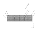
- FIG. 1 is a perspective view of an electronic component mounting board according to an embodiment of the present disclosure.
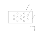
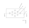
- FIG. 2 is a plan view of an electronic component mounting board according to an embodiment of the present disclosure.
- FIG. 3 is a plan view of an electronic component mounting board according to an embodiment of the present disclosure.
- FIG. 4 is a plan view of an electronic component mounting board according to an embodiment of the present disclosure.
- FIG. 5 is a plan view of an electronic component mounting board according to an embodiment of the present disclosure.
- FIG. 6 is a plan view of an electronic component mounting board according to an embodiment of the present disclosure.
- FIG. 7 is a cross-sectional view taken along the line AA of FIG. 2 of the electronic component mounting board according to the embodiment of the present disclosure.
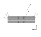
- FIG. 8 is a sectional view taken along line BB of FIG.
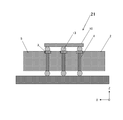
- FIG. 9 is a cross-sectional view of an electronic device according to an embodiment of the present disclosure.
- FIG. 10 is a cross-sectional view of an electronic device according to an embodiment of the present disclosure.
- FIG. 11 is a cross-sectional view of an electronic device according to an embodiment of the present disclosure.
- FIG. 12 is a plan view of an electronic component mounting board according to an embodiment of the present disclosure.
- FIG. 13 is a cross-sectional view of the electronic component mounting board according to the embodiment of the present disclosure, taken along line CC of FIG. 12.
- the electronic device 21 has a configuration in which the electronic component 10 is mounted on the electronic component mounting board 1. Either direction of the electronic component mounting board 1 and the electronic device 21 may be upward or downward, but for convenience, the orthogonal coordinate system xyz is defined and the positive side in the z direction is upward.
- the electronic component 10 is, for example, an optical semiconductor element such as a capacitor, an LD (Laser diode) or a PD (Photo Diode), or an imaging element such as a CCD (Charge Coupled Device) type or a CMOS (Complementary Metal Oxide Semiconductor) type. It may be.
- the electronic component 10 may be a light emitting element such as an LED (Light Emitting Diode) or an integrated circuit such as an LSI (Large Scale Integration).
- the electronic component mounting substrate 1 has a substrate 2.
- the substrate 2 may have a flat plate portion and a frame portion located on the flat plate portion, or may have only the frame portion or only the flat plate portion.
- the electronic component mounting board 1 has a frame portion and a flat plate portion.
- the substrate 2 refers to an insulating base including a frame portion, a flat plate portion, and both.
- the substrate 2 has one or more insulating layers 5.
- Examples of the electrically insulating ceramics used as the material of the insulating layer 5 forming the frame portion and the flat plate portion include, for example, an aluminum oxide sintered body, a mullite sintered body, a silicon carbide sintered body, and an aluminum nitride sintered body. Body, a silicon nitride sintered body, a glass ceramic sintered body, or the like.
- the resin used as the material of the insulating layer 5 forming the frame portion and the flat plate portion may be, for example, a thermoplastic resin, an epoxy resin, a polyimide resin, an acrylic resin, a phenol resin, a fluorine resin, or the like.
- As the fluorine-based resin for example, polyester resin or tetrafluoroethylene resin may be used.
- the substrate 2 may be formed of only the frame portion or only the flat plate portion, or the flat plate portion may be formed on the upper surface of the frame portion or the lower surface of the frame portion, or on the upper surface of the frame portion and the lower surface of the frame portion. It may be formed by stacking.
- the substrate 2 including the frame portion and the flat plate portion may be formed of six insulating layers 5 as shown in FIGS. 1 to 3, or may be formed of five or less insulating layers 5 or seven or more insulating layers 5. May be. When the number of insulating layers 5 is 5 or less, the electronic component mounting substrate 1 can be thinned. Further, when the insulating layer 5 has six or more layers, the rigidity of the electronic component mounting substrate 1 can be increased.
- the size of one side of the outermost periphery of the substrate 2 may be, for example, 0.3 mm to 10 cm.
- the substrate 2 When the substrate 2 has a rectangular shape in a plan view, it may have a square shape or a rectangular shape.
- the thickness of the substrate 2 may be 0.2 mm or more.
- the frame part and the flat plate part may be made of the same material or different materials.
- the frame part and the flat plate part can be fired at the same temperature.
- the obtained frame portion and the flat plate have similar basic physical properties such as a coefficient of thermal expansion, when the electronic component 10 generates heat after mounting the electronic component 10, cracks due to a difference in thermal expansion and the like are generated. Is less likely to occur.
- a material can be selected according to the case.
- the electrode pad 3 may be located on the upper surface of the frame portion, the upper surface of the flat plate portion, or the lower surface of the flat plate portion. Further, on the upper surface or the lower surface of the flat plate portion, the internal wirings 6 formed between the insulating layers 5 and the internal wirings 6 or the plurality of via conductors 4 for vertically connecting the electrode pads 3 and the internal wirings 6 and the like are located. May be The internal wiring 6 or the via conductor 4 may have a part of the internal wiring 6 or the via conductor 4 exposed on the surface of the substrate 2. The via conductor 4 penetrates the insulating layer 5 in the thickness direction of the substrate 2.
- the electrode pad 3, the internal wiring 6 and the via conductor 4 are made of the insulating layer 5 made of tungsten (W), molybdenum (Mo), manganese (Mn), silver (Ag), or copper. (Cu) may be included.
- the electrode pad 3, the internal wiring 6, and the via conductor 4 are made of tungsten (W), molybdenum (Mo), manganese (Mn), silver (Ag), or copper (.
- An alloy containing at least one metal material of Cu may be included.
- the electrode pad 3, the internal wiring 6, and the via conductor 4 have insulating layers 5 made of copper (Cu), gold (Au), aluminum (Al), nickel (Ni), molybdenum (Mo), Alternatively, it may contain titanium (Ti).
- the electrode pad 3, the internal wiring 6, and the via conductor 4 are made of copper (Cu), gold (Au), aluminum (Al), nickel (Ni), molybdenum (Mo), or An alloy containing at least one metal material of titanium (Ti) may be included.
- a plurality of via conductors 4 are arranged in (m) columns in the X direction and (n) rows in the Y direction (m and n are natural numbers). When viewed in a plan view, the via conductors 4 are located only on the odd-numbered rows of the odd-numbered columns and the even-numbered rows of the even-numbered columns, or only on the even-numbered rows of the odd-numbered columns and the odd-numbered rows of the even-numbered columns. ..
- the arrangement of the via conductors 4 described here corresponds to the grid-like grid. At this time, the natural number is a general natural number in mathematics and is a positive integer.
- m and n may be the same natural numbers when the column intervals and the row intervals in which the plurality of via conductors 4 are arranged are the same. If the column intervals and the row intervals in which the plurality of via conductors 4 are arranged are the same and m and n are the same natural numbers, the electrical resistance is applied to the electronic component mounting substrate 1 more uniformly. it can.
- the electronic component mounting substrate 1 according to the embodiment of the present disclosure has the above-described configuration, so that the electrical resistance value of the electronic component mounting substrate 1 is kept low and the flatness of the electronic component mounting substrate 1 is maintained. Can be kept.
- the electronic component mounting board 1 of the present disclosure reduces the resistance value of the electronic component mounting board 1 and maintains the flatness of the electronic component mounting board 1 by the arrangement of the via conductors 4 described above. be able to.
- the board 2 may have a feeding point 7 at the end of the board 2 when seen in a plan view.
- the plurality of via conductors 4 may be more in the second row than in the first row near the feeding point 7.
- the unnecessary via conductors 4 are not provided and the electronic component mounting board 1 is not provided.
- the electric resistance value can be lowered.
- the substrate 2 may have a first insulating layer 5a and a second insulating layer 5b.
- the first insulating layer 5a and the second insulating layer 5b have a plurality of via conductors 4, and, when seen through in a plan view, the plurality of via conductors 4 of the first insulating layer 5a and the plurality of second insulating layers 5b.
- the via conductor 4 may be located so as to at least partially overlap.
- the plurality of via conductors 4 of the first insulating layer 5a and the plurality of via conductors 4 of the second insulating layer 5b are located at least partially overlapped with each other, the plurality of via conductors 4 of the first insulating layer 5a
- the process of manufacturing the plurality of via conductors 4 of the second insulating layer 5b can be simplified.
- the plane see-through in the present disclosure refers to see-through to the negative side in the z direction shown in FIG. 1.
- first insulating layer 5a and the second insulating layer 5b have a plurality of via conductors 4, and, when seen through in a plan view, the plurality of via conductors 4 of the first insulating layer 5a and the second insulating layer 5b.
- the plurality of via conductors 4 may be located apart from each other. In other words, the plurality of via conductors 4 of the first insulating layer 5a and the plurality of via conductors 4 of the second insulating layer 5b do not have to be overlapped with each other when seen in a plan view.
- the plurality of via conductors 4 of the first insulating layer 5a and the plurality of via conductors 4 of the second insulating layer 5b are located apart from each other, it is possible to reduce the number of via conductors 4 in each layer of the insulating layer 5. In addition, the electric resistance value of the entire electronic component mounting board 1 can be reduced.
- three adjacent via conductors 4 may be positioned in an equilateral triangle.
- the electronic component mounting board 1 can have a uniform electric resistance value.
- a plating layer may be provided on the exposed surfaces of the electrode pad 3, the internal wiring 6, and the via conductor 4.
- the exposed surface of the electrode pad 3, the internal wiring 6, and the via conductor 4 for external circuit connection can be reduced in oxidation by the plating layer.
- the electronic device 21 includes the electronic component mounting board 1 and the electronic component 10 mounted on the electronic component mounting board 1.
- the electronic device 21 includes the electronic component mounting board 1 and the electronic component 10 mounted on the electronic component mounting board 1.
- the electronic component 10 may be an image pickup device such as a CMOS (Complementary Metal Oxide Semiconductor) or a CCD (Charge Coupled Device).
- the electronic component 10 may be a light emitting element such as an LED (Light Emitting Diode) or an integrated circuit such as an LSI (Large Scale Integrated).
- the electronic component 10 may be arranged on the upper surface of the substrate 2 via an adhesive material. When the electronic component 10 is arranged on the upper surface of the substrate 2 via the adhesive material, the upper surface of the substrate 2 functions as a mounting area of the electronic component 10.
- the adhesive material for example, silver epoxy or thermosetting resin can be used.
- the electronic device 21 may have the lid 12.
- the lid 12 may cover the electronic component 10 and be bonded to the upper surface of the electronic component mounting substrate 1.
- the electronic component mounting board 1 may be connected to the lid body 12 on the upper surface of the frame portion, or may be a frame shape provided to support the lid body 12 and to surround the electronic component 10 on the upper surface of the substrate 2.
- a body may be provided.
- the frame-shaped body and the substrate 2 may be made of the same material, or may be made of different materials.
- the substrate 2 and the frame-shaped body may be provided with openings to be integrated with the uppermost insulating layer 5, or the substrate 2 may be formed.
- the frame and the frame-shaped body may be joined with a brazing material or the like.
- the frame-shaped body may be the same material as the lid-body bonding material 14 that joins the lid 12 and the substrate 2.
- the lid joining material 14 may be, for example, a thermosetting resin, low melting point glass, or a brazing material containing a metal component.
- the frame-shaped body and the lid body 12 may be integrally configured.
- the lid 12 may be made of a highly transparent member such as a glass material when the electronic component 10 is an imaging device such as a CMOS or CCD or a light emitting device such as an LED.
- the lid 12 may be made of a metal material or an organic material when the electronic component 10 is an integrated circuit or the like.
- the lid 12 is joined to the electronic component mounting substrate 1 via the lid joining material 14.
- a material forming the lid-bonding material 14 for example, a thermosetting resin, low melting point glass, or a brazing material containing a metal component can be used.
- a ceramic green sheet forming the substrate 2 is formed.
- the substrate 2 which is mainly an aluminum oxide (Al 2 O 3 ) sintered body
- Al 2 O 3 powder is used as a sintering aid in silica (SiO 2 )
- MgO magnesia
- CaO calcia
- a mixture obtained by further adding an appropriate binder, solvent and plasticizer to the Al 2 O 3 powder is kneaded to form a slurry.
- the ceramic green sheet for multi-cavity production can be obtained by subjecting the slurry mixture to a forming method such as a doctor blade method or a calender roll method.
- the substrate 2 mainly contains a resin
- a mold that can be molded into a predetermined shape is used to mold the resin before curing by a transfer molding method or an injection molding method to form the substrate 2. can do.
- the substrate 2 may be formed by impregnating a base material containing glass fibers with a resin, such as glass epoxy resin.
- the substrate 2 can be formed by impregnating a base material containing glass fibers with an epoxy resin precursor and thermally curing the epoxy resin precursor at a predetermined temperature.
- the metal paste will be the electrode pad 3, the electrode pad for external circuit connection, the internal wiring 6, and the via conductor 4 of the ceramic green sheet obtained in the step (1) by the screen printing method or the like. Apply or fill.
- This metal paste is prepared by adding a suitable solvent and a binder to the metal powder containing the above-mentioned metal material and kneading the mixture to adjust the viscosity to an appropriate level.
- the metal paste may contain glass or ceramics in order to increase the bonding strength with the substrate 2.
- the electrode pad 3, the electrode pad for connecting an external circuit, the internal wiring 6 and the via conductor 4 can be manufactured by a sputtering method, a vapor deposition method or the like.
- the concave portion may be provided at a predetermined position of the green sheet to be the substrate 2 by using a die, punching, laser, or the like.
- the ceramic green sheet laminate to be the insulating layer 5 substrate 2 (electronic component mounting substrate 1) may be manufactured by the steps (1) to (4) described above. Further, the recess may be provided at a predetermined position of the ceramic green sheet laminate. The recess may be provided by stacking a plurality of ceramic green sheets, and a metal mold, punching, laser, or the like is used for the ceramic green sheet when forming the through hole at the position to be the recess after firing. May be.
- the ceramic green sheet laminate is fired at a temperature of about 1500° C. to 1800° C. to obtain a multi-cavity wiring board in which a plurality of boards 2 (electronic component mounting board 1) are arranged.
- the above-mentioned metal paste is fired at the same time as the ceramic green sheet that becomes the substrate 2 (electronic component mounting substrate 1), and becomes the electrode pad 3, the internal wiring 6, and the via conductor 4.
- a method can be used in which a dividing groove is formed in the multi-cavity wiring board along the outer edge of the board 2 (electronic component mounting board 1) and the dividing groove is broken and divided. ..
- a method such as cutting along the outer edge of the substrate 2 (electronic component mounting substrate 1) by a slicing method or the like.
- the dividing groove may be formed by cutting the divided groove with a slicing device to have a thickness smaller than that of the multi-piece wiring board after firing.
- the dividing groove may be formed by pressing a cutter blade against the ceramic green sheet laminate for a multi-cavity wiring board, or by cutting with a slicing device to a thickness smaller than the thickness of the ceramic green sheet laminate.
- the above-described multi-cavity wiring board uses electrolysis to divide the electrode pads 3, the electrode pads for external circuit connection, and the exposed wiring conductors before division into a plurality of boards 2 (electronic component mounting board 1). Plating may be applied.
- the electrode pad 3, the electrode pad for external circuit connection, and the exposed wiring conductor are plated with an electric field after dividing the multi-cavity wiring board into a plurality of boards 2 (electronic component mounting board 1). You may.
- the substrate 2 is a resin, it can be cut using, for example, a slicing method, a laser cutting method, or the like.
- the electronic component 10 is mounted on the upper surface or the lower surface of the electronic component mounting board 1.
- a region of the surface of the electronic component mounting substrate 1 on which the electronic component 10 is mounted is defined as a mounting region.
- the electronic component 10 is electrically joined to the electronic component mounting substrate 1 by an electronic component connecting material 13 such as wire bonding.
- the electronic component 10 may be fixed to the electronic component mounting substrate 1 by providing an adhesive or the like on the electronic component 10 or the electronic component mounting substrate 1.
- the electronic component mounting board 1 and the lid 12 may be joined using the lid joining material 14 after the electronic component 10 is mounted in the mounting region of the electronic component mounting substrate 1.
- An electronic device 21 is manufactured by manufacturing the electronic component mounting substrate 1 as in the above steps (1) to (8) and mounting the electronic component 10 in the mounting region of the electronic component mounting substrate 1. You can The order of the steps (1) to (8) and the number of steps are not specified. Further, it is not necessary to go through all the steps (1) to (8) described above.
- the present disclosure is not limited to the example of the above-described embodiment. Further, each configuration can be modified in various ways such as numerical values. Further, for example, in the example shown in FIGS. 1 to 11, the shape of the electrode pad 3 is rectangular when viewed in cross section, but may be circular or other polygonal shape. Further, the arrangement, the number, the shape, the mounting method of the electronic component 10 and the like of the electrode pads 3 according to the embodiment of the present disclosure are not specified. It should be noted that various combinations in the embodiment of the present disclosure are not limited to the examples of the above embodiment.
- Electrode pad 4 Via conductor 5... Insulating layer 5a... First insulating layer 5b... 2 Insulating layer 6... Internal wiring 7... Feed point 10... Electronic component 12... Lid 13... Electronic component bonding material 21... Electronic device
Landscapes
- Engineering & Computer Science (AREA)
- Microelectronics & Electronic Packaging (AREA)
- Chemical & Material Sciences (AREA)
- Ceramic Engineering (AREA)
- Inorganic Chemistry (AREA)
- Structure Of Printed Boards (AREA)
- Production Of Multi-Layered Print Wiring Board (AREA)
Abstract
本開示の一実施形態に係る電子部品実装用基板は、基板と、複数のビア導体とを備える。基板は、電子部品が実装される実装領域と、絶縁層を1層以上有する。複数のビア導体は、基板の厚み方向に絶縁層を貫通する。複数のビア導体は、絶縁層を平面視した場合に、X方向に(m)列、Y方向に(n)行(m,nは自然数)に並び、奇数列の奇数行目かつ偶数列の偶数行目のみ、または、奇数列の偶数行目かつ偶数列の奇数行目のみのどちらかに位置する。
Description
本開示は、電子部品が実装される電子部品実装用基板および電子装置に関する。
絶縁層を含む配線基板を備えた電子部品実装用基板が知られている。また、このような電子部品実装用基板に電子部品が実装された電子装置が知られている(特許文献1参照)。
本開示の一実施形態に係る電子部品実装用基板は、基板と、複数のビア導体とを備える。基板は、電子部品が実装される実装領域と、絶縁層を1層以上有する。複数のビア導体は、基板の厚み方向に絶縁層を貫通する。複数のビア導体は、絶縁層を平面視した場合に、X方向に(m)列、Y方向に(n)行(m,nは自然数)に並び、奇数列の奇数行目かつ偶数列の偶数行目のみ、または、奇数列の偶数行目かつ偶数列の奇数行目のみのどちらかに位置する。
本開示の一実施形態に係る電子装置は、電子部品実装用基板と、電子部品実装用基板に実装された電子部品とを備えている。
<電子部品実装用基板1および電子装置21の構成>
図面を参照し、本開示のいくつかの例示的な実施形態を説明する。なお、以下の説明では、電子部品実装用基板1に電子部品10が実装された構成を電子装置21とする。電子部品実装用基板1および電子装置21は、いずれの方向が上方若しくは下方とされてもよいが、便宜的に、直交座標系xyzを定義するとともに、z方向の正側を上方とする。また、電子部品10は、例えば、コンデンサ、LD(Laser diode)またはPD(Photo Diode)等の光半導体素子あるいは、CCD(Charge Coupled Device)型またはCMOS(Complementary Metal Oxide Semiconductor)型等の撮像素子であってもよい。また、電子部品10は、LED(Light Emitting Diode)等の発光素子またはLSI(Large Scale Integration)等の集積回路等であってもよい。
図面を参照し、本開示のいくつかの例示的な実施形態を説明する。なお、以下の説明では、電子部品実装用基板1に電子部品10が実装された構成を電子装置21とする。電子部品実装用基板1および電子装置21は、いずれの方向が上方若しくは下方とされてもよいが、便宜的に、直交座標系xyzを定義するとともに、z方向の正側を上方とする。また、電子部品10は、例えば、コンデンサ、LD(Laser diode)またはPD(Photo Diode)等の光半導体素子あるいは、CCD(Charge Coupled Device)型またはCMOS(Complementary Metal Oxide Semiconductor)型等の撮像素子であってもよい。また、電子部品10は、LED(Light Emitting Diode)等の発光素子またはLSI(Large Scale Integration)等の集積回路等であってもよい。
電子部品実装用基板1は、基板2を有する。基板2は、平板部と平板部上に位置した枠部とを有してもよいし、枠部のみ、または、平板部のみを有しても良い。なお、図1~図3に示す例では、電子部品実装用基板1は、枠部と、平板部とを有している。
枠部および平板部を構成する絶縁層5の材料は例えば、電気絶縁性セラミックスまたは樹脂(例えば、プラスティックス、熱可塑性樹脂)等が使用される。なお、本明細書において、基板2は、枠部、平板部、およびその両方を含む絶縁基体のことを指す。基板2は、絶縁層5を1層以上有している。
枠部および平板部を形成する絶縁層5の材料として使用される電気絶縁性セラミックスとしては例えば、酸化アルミニウム質焼結体、ムライト質焼結体、炭化珪素質焼結体、窒化アルミニウム質焼結体、窒化珪素質焼結体またはガラスセラミック焼結体等である。枠部、平板部を形成する絶縁層5の材料として使用される樹脂としては例えば、熱可塑性の樹脂、エポキシ樹脂、ポリイミド樹脂、アクリル樹脂、フェノール樹脂またはフッ素系樹脂等を用いてもよい。フッ素系樹脂としては例えば、ポリエステル樹脂または四フッ化エチレン樹脂等を用いてもよい。
基板2は、前述したように、枠部のみ、平板部のみで形成されていてもよいし、枠部の上面または枠部の下面、または、枠部の上面および枠部の下面に平板部を積層して形成されていてもよい。
枠部、平板部を含む基板2は、図1~図3に示すように6層の絶縁層5から形成されていてもよいし、5層以下または7層以上の絶縁層5から形成されていてもよい。絶縁層5が5層以下の場合には、電子部品実装用基板1の薄型化を図ることができる。また、絶縁層5が6層以上の場合には、電子部品実装用基板1の剛性を高めることができる。
基板2は例えば、最外周の1辺の大きさは0.3mm~10cmであってもよい。基板2は、平面視した場合に、基板2が矩形状であるとき、正方形であってもよいし長方形であってもよい。また基板2の厚みは0.2mm以上であってもよい。
枠部と平板部は、同一の材料であっても良いし、異なる材料であっても良い。枠部と平板部とが同一の材料であるときには、枠部と平板部とを同じ温度で焼成することができる。また、得られた枠部および平板は、熱膨張率等の基本的な物性が近似したものとなるため、電子部品10を実装した後に電子部品10が発熱した場合に、熱膨張差によるクラック等の発生が少ない。また、枠部と平板部とが異なる材料であるときには、場合に応じた素材を選択することができる。
枠部、平板部の上面または平板部の下面には、電極パッド3が位置していてもよい。また、平板部の上面または下面には、絶縁層5間に形成される内部配線6および内部配線6同士あるいは、電極パッド3と内部配線6等を上下に接続する複数のビア導体4が位置していてもよい。これら内部配線6またはビア導体4は、基板2の表面に内部配線6またはビア導体4の一部が露出していてもよい。ビア導体4は、基板2の厚み方向に絶縁層5を貫通している。
絶縁層5が電気絶縁性セラミックスを含む場合、電極パッド3、内部配線6およびビア導体4は、絶縁層5タングステン(W)、モリブデン(Mo)、マンガン(Mn)、銀(Ag)、若しくは銅(Cu)を含んでいてもよい。また、絶縁層5が電気絶縁性セラミックスを含む場合、電極パッド3、内部配線6およびビア導体4は、タングステン(W)、モリブデン(Mo)、マンガン(Mn)、銀(Ag)、若しくは銅(Cu)のうち少なくとも1種以上の金属材料を含有する合金等を含んでいてもよい。
絶縁層5が樹脂を含む場合、電極パッド3、内部配線6およびビア導体4は、絶縁層5銅(Cu)、金(Au)、アルミニウム(Al)、ニッケル(Ni)、モリブデン(Mo)、若しくはチタン(Ti)を含んでいてもよい。また、絶縁層5が樹脂を含む場合、電極パッド3、内部配線6およびビア導体4は、銅(Cu)、金(Au)、アルミニウム(Al)、ニッケル(Ni)、モリブデン(Mo)、若しくはチタン(Ti)のうち少なくとも1種以上の金属材料を含有する合金等を含んでいてもよい。
複数のビア導体4は、X方向に(m)列、Y方向に(n)行(m,nは自然数)並んで配置されている。ビア導体4は、平面視した場合に、奇数列の奇数行目かつ偶数列の偶数行目のみ、または、奇数列の偶数行目かつ偶数列の奇数行目のみのどちらかに位置している。ここに記載のビア導体4の配置は、格子状のマス目に応じたものである。このとき、自然数は数学の一般的な自然数のことであり、正の整数である。ビア導体4は格子状に位置していることによって、電子部品実装用基板1に対して均一に電気抵抗がかかるようにできる。また、複数のビア導体4が配置される列の間隔および行の間隔が同じ場合において、mとnは、同じ自然数であってもよい。複数のビア導体4が配置される列の間隔および行の間隔が同じであるとともに、mとnが同じ自然数であれば、電子部品実装用基板1に対して一層均一に電気抵抗がかかるようにできる。
本開示の一実施形態に係る電子部品実装用基板1は、上述した構成であることによって、電子部品実装用基板1の電気抵抗値を低く保ち、かつ、電子部品実装用基板1の平坦性を保つことができる。
なお、ビア導体が密集している電子部品実装用基板である場合、電気抵抗値を下げることができたとしても熱変形等によって基板の平坦性が損なわれるおそれがある。これに対し、本開示の電子部品実装用基板1は、上述したビア導体4の配置により、電子部品実装用基板1の抵抗値を低くし、かつ、電子部品実装用基板1の平坦性を保つことができる。
基板2は、平面視した場合に、基板2の端部に給電点7を有していてもよい。基板2が給電点7を有しているとき、複数のビア導体4は、給電点7に近い第1列より、第2列の数が多くなっていてもよい。給電点7に近い第1列のビア導体4の数よりも、第2列のビア導体4の数が多くなっているときには、不要なビア導体4を設けることなく、電子部品実装用基板1の電気抵抗値を下げることができる。
基板2は、第1絶縁層5aおよび第2絶縁層5bを有していてもよい。第1絶縁層5aおよび第2絶縁層5bは、複数のビア導体4を有しているとともに、平面透視した場合、第1絶縁層5aの複数のビア導体4と、第2絶縁層5bの複数のビア導体4とが少なくとも一部が重なって位置していてもよい。第1絶縁層5aの複数のビア導体4と、第2絶縁層5bの複数のビア導体4とが少なくとも一部が重なって位置している場合、第1絶縁層5aの複数のビア導体4と、第2絶縁層5bの複数のビア導体4とを作製する工程を簡略化できる。なお、本開示での平面透視とは、図1に示すz方向の負側に透視することを指す。
また、第1絶縁層5aおよび第2絶縁層5bは、複数のビア導体4を有しているとともに、平面透視した場合、第1絶縁層5aの複数のビア導体4と、第2絶縁層5bの複数のビア導体4とが離れて位置していてもよい。言い換えれば、平面透視した場合、第1絶縁層5aの複数のビア導体4と、第2絶縁層5bの複数のビア導体4とが重なって位置しいなくてもよい。第1絶縁層5aの複数のビア導体4と、第2絶縁層5bの複数のビア導体4とが離れて位置しているときには、絶縁層5の各層で、ビア導体4の数を減らすことができるとともに、電子部品実装用基板1全体の電気抵抗値を低くできる。
基板2を平面視した場合、複数のビア導体4は、複数のビア導体4のうち近接している3つのビア導体4が正三角形に位置していていてもよい。近接している3つのビア導体4が平面視した場合に正三角形に位置しているときには、電子部品実装用基板1が均一な電気抵抗値を生じるようにできる。
電極パッド3、内部配線6およびビア導体4の露出表面に、めっき層が設けられてもよい。外部回路接続用の電極パッド3、内部配線6およびビア導体4の露出表面は、めっき層によって酸化を低減できる。
<電子装置21の構成>
電子装置21の例を図1~図3に示す。電子装置21は、電子部品実装用基板1と、電子部品実装用基板1に実装された電子部品10を備えている。
電子装置21の例を図1~図3に示す。電子装置21は、電子部品実装用基板1と、電子部品実装用基板1に実装された電子部品10を備えている。
電子装置21は、電子部品実装用基板1と、電子部品実装用基板1に実装された電子部品10を有している。電子部品10は、例えばCMOS(Complementary Metal Oxide Semiconductor)、CCD(Charge Coupled Device)等の撮像素子であってもよい。または、電子部品10は、LED(Light Emitting Diode)等の発光素子、あるいは、LSI(Large Scale Integrated)等の集積回路等であってもよい。なお、電子部品10は、接着材を介して、基板2の上面に配置されていてもよい。電子部品10が、接着材を介して、基板2の上面に配置されるとき、基板2の上面は電子部品10の実装領域として機能する。接着材は、例えば、銀エポキシまたは熱硬化性樹脂等を用いることができる。
電子装置21は、蓋体12を有していてもよい。蓋体12は、電子部品10を覆うとともに、電子部品実装用基板1の上面に接合されていてもよい。ここで、電子部品実装用基板1は枠部の上面で蓋体12と接続してもよいし、蓋体12支え、基板2の上面であって電子部品10を取り囲むように設けられた枠状体を設けてもよい。また、枠状体と基板2とは同じ材料から構成されていてもよいし、別の材料で構成されていてもよい。
枠状体と基板2と、が同じ材料である場合、基板2と枠状体とは開口部を設けて最上層の絶縁層5と一体化するように作られていてもよいし、基板2と枠状体とを、ろう材等でそれぞれ接合してもよい。
また、基板2と枠状体とが別の材料である例として枠状体が蓋体12と基板2とを接合する蓋体接合材14と同じ材料である場合がある。このとき、蓋体接合材14を厚く設けることで、蓋体12および基板2を接着するとともに、蓋体12を支えることができる。蓋体接合材14は例えば熱硬化性樹脂または低融点ガラスまたは金属成分を含むろう材等が挙げられる。また、枠状体と蓋体12とが同じ材料である場合は、枠状体と蓋体12とが一体として構成されていてもよい。
蓋体12は、例えば電子部品10がCMOS、CCD等の撮像素子、またはLED等の発光素子である場合、ガラス材料等の透明度の高い部材が用いてもよい。また蓋体12は例えば、電子部品10が集積回路等であるとき、金属製材料または有機材料が用いられてもよい。
蓋体12は、蓋体接合材14を介して電子部品実装用基板1と接合している。蓋体接合材14を構成する材料として例えば、熱硬化性樹脂または低融点ガラスまたは金属成分を含むろう材等を用いることができる。
<電子部品実装用基板1および電子装置21の製造方法>
次に、本開示の一実施形態の電子部品実装用基板1および電子装置21の製造方法の一例を説明する。なお、下記で示す本開示の一実施形態の電子部品実装用基板1および電子装置21の製造方法の一例は、多数個取り配線基板を用いた基板2の製造方法である。
次に、本開示の一実施形態の電子部品実装用基板1および電子装置21の製造方法の一例を説明する。なお、下記で示す本開示の一実施形態の電子部品実装用基板1および電子装置21の製造方法の一例は、多数個取り配線基板を用いた基板2の製造方法である。
(1)まず、基板2を構成するセラミックグリーンシートを形成する。例えば、主に酸化アルミニウム(Al2O3)質焼結体である基板2を得る場合は、Al2O3の粉末に焼結助材としてシリカ(SiO2)、マグネシア(MgO)またはカルシア(CaO)等の粉末を添加する。そしてAl2O3の粉末に、適当なバインダー、溶剤および可塑剤を更に添加した混合物は、混錬することでスラリー状となる。多数個取り用のセラミックグリーンシートは、スラリー状の混合物に、ドクターブレード法またはカレンダーロール法等の成形方法を施すことで得ることができる。
なお、基板2が例えば主に樹脂を含む場合は、所定の形状に成形できるような金型を用いて、トランスファーモールド法またはインジェクションモールド法等で硬化前の樹脂を成形することによって基板2を形成することができる。また、基板2は、例えばガラスエポキシ樹脂のように、ガラス繊維を含む基材に樹脂を含浸させたものであってもよい。この場合には、ガラス繊維からを含む基材にエポキシ樹脂の前駆体を含浸させ、このエポキシ樹脂前駆体を所定の温度で熱硬化させることによって基板2を形成できる。
(2)次に、スクリーン印刷法等によって、金属ペーストが(1)の工程で得られたセラミックグリーンシートの電極パッド3、外部回路接続用の電極パッド、内部配線6およびビア導体4となる部分に塗布または充填する。この金属ペーストは、前述した金属材料を含む金属粉末に適当な溶剤およびバインダーを加えて混練することによって、適度な粘度に調整して作製する。なお、金属ペーストは、基板2との接合強度を高めるために、ガラスまたはセラミックスを含んでいても構わない。
また、基板2が樹脂を含む場合には、電極パッド3、外部回路接続用の電極パッド、内部配線6およびビア導体4は、スパッタ法、蒸着法等によって作製することができる。
(3)次に、前述のグリーンシートを金型等によって加工する。ここで凹部は、基板2となるグリーンシートの所定の箇所に、金型、パンチング、またはレーザー等を用いて設けてもよい。
(4)次に、各絶縁層5となるセラミックグリーンシートを積層し、加圧する。絶縁層5基板2(電子部品実装用基板1)となるセラミックグリーンシート積層体は、上述の(1)から(4)の工程により作製してもよい。また凹部は、セラミックグリーンシート積層体の所定の位置に設けてもよい。また、凹部は、複数のセラミックグリーンシート積層することで設けてもよく、焼成後に凹部となる位置に対して貫通孔を作製するにあたり、セラミックグリーンシートに、金型、パンチング、またはレーザー等を用いてもよい。
(5)次に、このセラミックグリーンシート積層体を約1500℃~1800℃の温度で焼成することで、基板2(電子部品実装用基板1)が複数配列された多数個取り配線基板を得る。なお、(5)の工程によって、前述した金属ペーストは、基板2(電子部品実装用基板1)となるセラミックグリーンシートと同時に焼成され、電極パッド3、内部配線6およびビア導体4となる。
(6)次に、基板2(電子部品実装用基板1)が複数配列された多数個取り配線基板の表面に、めっき等の表面処理を行う。
(7)次に、複数の基板2(電子部品実装用基板1)を、焼成して得られた多数個取り配線基板を分断することで得られる。分断では、基板2(電子部品実装用基板1)の外縁となる箇所に沿って多数個取り配線基板に分割溝を形成し、この分割溝に沿って破断させて分割する方法を用いることができる。あるいは、スライシング法等により基板2(電子部品実装用基板1)の外縁となる箇所に沿って切断する方法等を用いることができる。なお、分割溝は、焼成後にスライシング装置により多数個取り配線基板の厚みより小さく切り込むことによって形成してもよい。あるいは、分割溝は、多数個取り配線基板用のセラミックグリーンシート積層体にカッター刃を押し当てたり、スライシング装置によりセラミックグリーンシート積層体の厚みより小さく切り込んだりすることで形成してもよい。なお、上述した多数個取り配線基板は、複数の基板2(電子部品実装用基板1)に分割する前に電解を用いて、電極パッド3、外部回路接続用の電極パッドおよび露出した配線導体にめっきを被着させてもよい。または、電極パッド3、外部回路接続用の電極パッドおよび露出した配線導体は、多数個取り配線基板を複数の基板2(電子部品実装用基板1)分割した後に、電界を用いてめっきを被着してもよい。
基板2が樹脂の場合には、例えばスライシング法、レーザーカッティング法等を用いて分断することができる。
(8)次に、電子部品10を、電子部品実装用基板1の上面または下面に実装する。なお、電子部品実装用基板1の面のうち、電子部品10が実装される領域を実装領域とする。電子部品10はワイヤボンディング等の電子部品接続材13で電子部品実装用基板1と電気的に接合させる。またこのとき、電子部品10は、電子部品10または電子部品実装用基板1に接着剤等を設けることで、電子部品実装用基板1に固定してもよい。また、電子部品実装用基板1と蓋体12とは、電子部品10を電子部品実装用基板1の実装領域に実装した後に、蓋体接合材14を用いて接合してもよい。
以上(1)~(8)の工程のようにして電子部品実装用基板1を作製し、電子部品実装用基板1の実装領域に電子部品10を実装することで、電子装置21を作製することができる。なお、上記(1)~(8)の工程順番および、工程の回数等は指定されない。また、上述した(1)~(8)の工程の全てを経る必要はない。
なお、本開示は上述の実施形態の例に限定されるものではない。また、各構成は数値等の種々の変形が可能である。また、例えば、図1~図11に示す例では、電極パッド3の形状は、断面視した場合に、矩形状であるが、円形状あるいはその他の多角形状であってもかまわない。また、本開示の一実施形態における電極パッド3の配置、数、形状および電子部品10の実装方法等は指定されない。なお、本開示の一実施形態における種々の組み合わせは上述の実施形態の例に限定されるものでない。
1・・・・電子部品実装用基板
2・・・・基板
3・・・・電極パッド
4・・・・ビア導体
5・・・・絶縁層
5a・・・第1絶縁層
5b・・・第2絶縁層
6・・・・内部配線
7・・・・給電点
10・・・電子部品
12・・・蓋体
13・・・電子部品接合材
21・・・電子装置
2・・・・基板
3・・・・電極パッド
4・・・・ビア導体
5・・・・絶縁層
5a・・・第1絶縁層
5b・・・第2絶縁層
6・・・・内部配線
7・・・・給電点
10・・・電子部品
12・・・蓋体
13・・・電子部品接合材
21・・・電子装置
Claims (7)
- 電子部品が実装される実装領域と絶縁層を1層以上有する基板と、前記基板の厚み方向に前記絶縁層を貫通する、複数のビア導体と、を備え、
前記複数のビア導体は、前記絶縁層を平面視した場合に、X方向に(m)列、Y方向に(n)行(m,nは自然数)に並び、奇数列の奇数行目かつ偶数列の偶数行目のみ、または、奇数列の偶数行目かつ偶数列の奇数行目のみのどちらかに位置する、電子部品実装用基板。 - mとnは同じ自然数である、請求項1に記載の電子部品実装用基板。
- 前記基板は、平面視した場合に、端部に給電点を有し、
前記複数のビア導体は、前記給電点に近い第1列より、第2列の数が多い、請求項1または請求項2に記載の電子部品実装用基板。 - 前記基板は、第1絶縁層および第2絶縁層を有し、
前記第1絶縁層および前記第2絶縁層は、それぞれ前記複数のビア導体を有し、平面透視した場合に、前記第1絶縁層の前記複数のビア導体と、前記第2絶縁層の前記複数のビア導体とが少なくとも一部が重なって位置している、請求項1~3のいずれか1つに記載の電子部品実装用基板。 - 前記基板は、第1絶縁層および第2絶縁層を有し、
前記第1絶縁層および前記第2絶縁層は、それぞれ前記複数のビア導体を有し、平面透視した場合に、前記第1絶縁層の前記複数のビア導体と、前記第2絶縁層の前記複数のビア導体とが離れて位置している、請求項1~3のいずれか1つに記載の電子部品実装用基板。 - 平面視した場合、前記複数のビア導体のうち近接している3つのビア導体は正三角形に位置している、請求項1~5のいずれか1つに記載の電子部品実装用基板。
- 請求項1~6のいずれか1つに記載の電子部品実装用基板と、
前記実装領域に実装された電子部品と、を備える電子装置。
Priority Applications (3)
| Application Number | Priority Date | Filing Date | Title |
|---|---|---|---|
| CN201980085212.5A CN113272950A (zh) | 2018-12-25 | 2019-12-20 | 电子部件安装用基板以及电子装置 |
| US17/417,796 US20220078909A1 (en) | 2018-12-25 | 2019-12-20 | Electronic component mounting substrate and electronic device |
| JP2020563198A JP7209740B2 (ja) | 2018-12-25 | 2019-12-20 | 電子部品実装用基板および電子装置 |
Applications Claiming Priority (2)
| Application Number | Priority Date | Filing Date | Title |
|---|---|---|---|
| JP2018240989 | 2018-12-25 | ||
| JP2018-240989 | 2018-12-25 |
Publications (1)
| Publication Number | Publication Date |
|---|---|
| WO2020137878A1 true WO2020137878A1 (ja) | 2020-07-02 |
Family
ID=71128680
Family Applications (1)
| Application Number | Title | Priority Date | Filing Date |
|---|---|---|---|
| PCT/JP2019/050085 Ceased WO2020137878A1 (ja) | 2018-12-25 | 2019-12-20 | 電子部品実装用基板および電子装置 |
Country Status (4)
| Country | Link |
|---|---|
| US (1) | US20220078909A1 (ja) |
| JP (1) | JP7209740B2 (ja) |
| CN (1) | CN113272950A (ja) |
| WO (1) | WO2020137878A1 (ja) |
Families Citing this family (1)
| Publication number | Priority date | Publication date | Assignee | Title |
|---|---|---|---|---|
| JP2022185903A (ja) * | 2021-06-03 | 2022-12-15 | 株式会社村田製作所 | 高周波モジュール及び通信装置 |
Citations (4)
| Publication number | Priority date | Publication date | Assignee | Title |
|---|---|---|---|---|
| JPH09153679A (ja) * | 1995-11-30 | 1997-06-10 | Kyocera Corp | 積層ガラスセラミック回路基板 |
| WO2005029581A1 (ja) * | 2003-09-24 | 2005-03-31 | Ibiden Co.,Ltd. | インターポーザ、多層プリント配線板 |
| JP2018152508A (ja) * | 2017-03-14 | 2018-09-27 | イビデン株式会社 | プリント配線板 |
| JP2019079969A (ja) * | 2017-10-26 | 2019-05-23 | 京セラ株式会社 | 配線基板 |
Family Cites Families (13)
| Publication number | Priority date | Publication date | Assignee | Title |
|---|---|---|---|---|
| JP2503725B2 (ja) * | 1990-05-18 | 1996-06-05 | 日本電気株式会社 | 多層配線基板 |
| JP2551221B2 (ja) * | 1990-10-05 | 1996-11-06 | 日本電気株式会社 | セラミック多層配線基板のスルーホール構造 |
| JP2001044591A (ja) * | 1999-08-03 | 2001-02-16 | Ngk Spark Plug Co Ltd | 配線基板 |
| JP4564342B2 (ja) * | 2004-11-24 | 2010-10-20 | 大日本印刷株式会社 | 多層配線基板およびその製造方法 |
| US7081672B1 (en) * | 2005-03-07 | 2006-07-25 | Lsi Logic Corporation | Substrate via layout to improve bias humidity testing reliability |
| US7405473B1 (en) * | 2005-11-23 | 2008-07-29 | Altera Corporation | Techniques for optimizing electrical performance and layout efficiency in connectors with via placement and routing |
| JP4824397B2 (ja) * | 2005-12-27 | 2011-11-30 | イビデン株式会社 | 多層プリント配線板 |
| JP2010263056A (ja) * | 2009-05-07 | 2010-11-18 | Kyocera Corp | 回路基板およびバンプ付き回路基板ならびに電子装置 |
| US20110048775A1 (en) * | 2009-08-31 | 2011-03-03 | Ibiden Co., Ltd. | Printed wiring board and method for manufacturing the same |
| KR101161971B1 (ko) * | 2010-07-21 | 2012-07-04 | 삼성전기주식회사 | 다층 회로 기판 및 다층 회로 기판의 제조 방법 |
| US9565762B1 (en) * | 2013-12-06 | 2017-02-07 | Marvell Israel (M.I.S.L) Ltd. | Power delivery network in a printed circuit board structure |
| JP2017050391A (ja) * | 2015-09-01 | 2017-03-09 | 株式会社デンソー | 多層基板およびその製造方法 |
| JP6730960B2 (ja) * | 2017-05-24 | 2020-07-29 | 日本特殊陶業株式会社 | 配線基板 |
-
2019
- 2019-12-20 CN CN201980085212.5A patent/CN113272950A/zh active Pending
- 2019-12-20 US US17/417,796 patent/US20220078909A1/en not_active Abandoned
- 2019-12-20 WO PCT/JP2019/050085 patent/WO2020137878A1/ja not_active Ceased
- 2019-12-20 JP JP2020563198A patent/JP7209740B2/ja active Active
Patent Citations (4)
| Publication number | Priority date | Publication date | Assignee | Title |
|---|---|---|---|---|
| JPH09153679A (ja) * | 1995-11-30 | 1997-06-10 | Kyocera Corp | 積層ガラスセラミック回路基板 |
| WO2005029581A1 (ja) * | 2003-09-24 | 2005-03-31 | Ibiden Co.,Ltd. | インターポーザ、多層プリント配線板 |
| JP2018152508A (ja) * | 2017-03-14 | 2018-09-27 | イビデン株式会社 | プリント配線板 |
| JP2019079969A (ja) * | 2017-10-26 | 2019-05-23 | 京セラ株式会社 | 配線基板 |
Also Published As
| Publication number | Publication date |
|---|---|
| JPWO2020137878A1 (ja) | 2021-10-28 |
| US20220078909A1 (en) | 2022-03-10 |
| CN113272950A (zh) | 2021-08-17 |
| JP7209740B2 (ja) | 2023-01-20 |
Similar Documents
| Publication | Publication Date | Title |
|---|---|---|
| JP6496026B2 (ja) | 配線基板および電子装置 | |
| WO2019207884A1 (ja) | 電子素子実装用基板、電子装置、および電子モジュール | |
| JP2018121005A (ja) | 電子素子実装用基板、電子装置および電子モジュール | |
| JP7610654B2 (ja) | 電子素子実装用基板、電子装置、および電子モジュール | |
| JP7569885B2 (ja) | 電子素子実装用基板、電子装置および電子モジュール | |
| JP7210191B2 (ja) | 電子素子実装用基板、電子装置、および電子モジュール | |
| JP7209740B2 (ja) | 電子部品実装用基板および電子装置 | |
| JP6068157B2 (ja) | 多数個取り配線基板 | |
| JP7242870B2 (ja) | 実装基板および電子装置 | |
| JP6408341B2 (ja) | 撮像素子実装用基板、撮像装置および撮像モジュール | |
| JP2013077739A (ja) | 配線基板ならびにその配線基板を備えた電子装置および電子モジュール装置 | |
| JP2013207204A (ja) | 配線母基板 | |
| JP7209749B2 (ja) | 電子部品実装用基体および電子装置 | |
| JP2014045012A (ja) | 多数個取り配線基板 | |
| JP7565700B2 (ja) | 実装基板、電子装置、および電子モジュール | |
| US20240088011A1 (en) | Electronic element mounting substrate | |
| US20240282651A1 (en) | Electronic element mounting substrate | |
| JP7212783B2 (ja) | 電子素子実装用基板、電子装置、電子モジュールおよび電子素子実装用基板の製造方法 | |
| JP7227019B2 (ja) | 電子素子実装用基板、電子装置、および電子モジュール | |
| JP6955460B2 (ja) | 電子素子実装用基板、電子素子実装用母基板、電子装置および電子モジュール | |
| JP6017994B2 (ja) | 電子素子搭載用基板および電子装置 | |
| JP5653323B2 (ja) | 成形体および多数個取り配線基板 | |
| JP2014165315A (ja) | 電子素子搭載用基板および電子装置 |
Legal Events
| Date | Code | Title | Description |
|---|---|---|---|
| 121 | Ep: the epo has been informed by wipo that ep was designated in this application |
Ref document number: 19906108 Country of ref document: EP Kind code of ref document: A1 |
|
| ENP | Entry into the national phase |
Ref document number: 2020563198 Country of ref document: JP Kind code of ref document: A |
|
| NENP | Non-entry into the national phase |
Ref country code: DE |
|
| 122 | Ep: pct application non-entry in european phase |
Ref document number: 19906108 Country of ref document: EP Kind code of ref document: A1 |