WO2020110987A1 - 平面コイルおよびこれを備える変圧器、無線送電器、電磁石 - Google Patents
平面コイルおよびこれを備える変圧器、無線送電器、電磁石 Download PDFInfo
- Publication number
- WO2020110987A1 WO2020110987A1 PCT/JP2019/045939 JP2019045939W WO2020110987A1 WO 2020110987 A1 WO2020110987 A1 WO 2020110987A1 JP 2019045939 W JP2019045939 W JP 2019045939W WO 2020110987 A1 WO2020110987 A1 WO 2020110987A1
- Authority
- WO
- WIPO (PCT)
- Prior art keywords
- metal layer
- metal
- metal particles
- planar coil
- coil according
- Prior art date
- Legal status (The legal status is an assumption and is not a legal conclusion. Google has not performed a legal analysis and makes no representation as to the accuracy of the status listed.)
- Ceased
Links
Images




Classifications
-
- H—ELECTRICITY
- H01—ELECTRIC ELEMENTS
- H01F—MAGNETS; INDUCTANCES; TRANSFORMERS; SELECTION OF MATERIALS FOR THEIR MAGNETIC PROPERTIES
- H01F17/00—Fixed inductances of the signal type
- H01F17/0006—Printed inductances
-
- H—ELECTRICITY
- H01—ELECTRIC ELEMENTS
- H01B—CABLES; CONDUCTORS; INSULATORS; SELECTION OF MATERIALS FOR THEIR CONDUCTIVE, INSULATING OR DIELECTRIC PROPERTIES
- H01B1/00—Conductors or conductive bodies characterised by the conductive materials; Selection of materials as conductors
- H01B1/20—Conductive material dispersed in non-conductive organic material
- H01B1/22—Conductive material dispersed in non-conductive organic material the conductive material comprising metals or alloys
-
- H—ELECTRICITY
- H01—ELECTRIC ELEMENTS
- H01F—MAGNETS; INDUCTANCES; TRANSFORMERS; SELECTION OF MATERIALS FOR THEIR MAGNETIC PROPERTIES
- H01F27/00—Details of transformers or inductances, in general
- H01F27/28—Coils; Windings; Conductive connections
- H01F27/2847—Sheets; Strips
-
- H—ELECTRICITY
- H01—ELECTRIC ELEMENTS
- H01F—MAGNETS; INDUCTANCES; TRANSFORMERS; SELECTION OF MATERIALS FOR THEIR MAGNETIC PROPERTIES
- H01F38/00—Adaptations of transformers or inductances for specific applications or functions
- H01F38/14—Inductive couplings
-
- H—ELECTRICITY
- H01—ELECTRIC ELEMENTS
- H01F—MAGNETS; INDUCTANCES; TRANSFORMERS; SELECTION OF MATERIALS FOR THEIR MAGNETIC PROPERTIES
- H01F5/00—Coils
- H01F5/003—Printed circuit coils
-
- H—ELECTRICITY
- H01—ELECTRIC ELEMENTS
- H01F—MAGNETS; INDUCTANCES; TRANSFORMERS; SELECTION OF MATERIALS FOR THEIR MAGNETIC PROPERTIES
- H01F7/00—Magnets
- H01F7/06—Electromagnets; Actuators including electromagnets
- H01F2007/068—Electromagnets; Actuators including electromagnets using printed circuit coils
-
- H—ELECTRICITY
- H01—ELECTRIC ELEMENTS
- H01F—MAGNETS; INDUCTANCES; TRANSFORMERS; SELECTION OF MATERIALS FOR THEIR MAGNETIC PROPERTIES
- H01F17/00—Fixed inductances of the signal type
- H01F17/0006—Printed inductances
- H01F2017/0073—Printed inductances with a special conductive pattern, e.g. flat spiral
-
- H—ELECTRICITY
- H01—ELECTRIC ELEMENTS
- H01F—MAGNETS; INDUCTANCES; TRANSFORMERS; SELECTION OF MATERIALS FOR THEIR MAGNETIC PROPERTIES
- H01F27/00—Details of transformers or inductances, in general
- H01F27/24—Magnetic cores
-
- H—ELECTRICITY
- H01—ELECTRIC ELEMENTS
- H01F—MAGNETS; INDUCTANCES; TRANSFORMERS; SELECTION OF MATERIALS FOR THEIR MAGNETIC PROPERTIES
- H01F27/00—Details of transformers or inductances, in general
- H01F27/28—Coils; Windings; Conductive connections
- H01F27/2804—Printed windings
-
- H—ELECTRICITY
- H01—ELECTRIC ELEMENTS
- H01F—MAGNETS; INDUCTANCES; TRANSFORMERS; SELECTION OF MATERIALS FOR THEIR MAGNETIC PROPERTIES
- H01F41/00—Apparatus or processes specially adapted for manufacturing or assembling magnets, inductances or transformers; Apparatus or processes specially adapted for manufacturing materials characterised by their magnetic properties
- H01F41/02—Apparatus or processes specially adapted for manufacturing or assembling magnets, inductances or transformers; Apparatus or processes specially adapted for manufacturing materials characterised by their magnetic properties for manufacturing cores, coils, or magnets
- H01F41/04—Apparatus or processes specially adapted for manufacturing or assembling magnets, inductances or transformers; Apparatus or processes specially adapted for manufacturing materials characterised by their magnetic properties for manufacturing cores, coils, or magnets for manufacturing coils
- H01F41/041—Printed circuit coils
- H01F41/043—Printed circuit coils by thick film techniques
Definitions
- the present disclosure relates to a planar coil, a transformer including the planar coil, a wireless power transmitter, and an electromagnet.
- Laminar coil can be obtained by preparing a plurality of flat coils with a spiral metal layer formed on an insulating base and stacking these.
- Patent Document 1 discloses a laminated coil in which a coil pattern is formed on an insulating substrate by electroforming plating.
- the plane coil of the present disclosure is made of ceramics and has a base body having a first surface and a first metal layer having a void and located on the first surface.
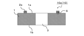
- FIG. 2 is an example of a cross-sectional view taken along the line A-A′ in FIG. 1. It is an example of the enlarged view in the S section shown in FIG. It is the top view which looked at other examples of the plane coil of this indication from the 1st surface side.
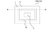
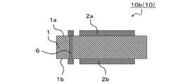
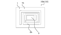
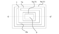
- FIG. 5 is a sectional view taken along line B-B′ of FIG. 4. It is the top view which looked at the plane coil of FIG. 4 from the 2nd surface side. It is the top view which looked at other examples of the plane coil of this indication from the 1st surface side.
- FIG. 8 is an example of a cross-sectional view taken along the line C-C′ of FIG. 7.
- FIG. 9 is another example of a cross-sectional view taken along the line C-C′ of FIG. 7. It is an example of the enlarged view in the S section shown in FIG.
- FIG. 2 is an example of a cross-sectional view taken along the line A-A′ in FIG. 1.
- A is a perspective view of the transformer of this indication.
- B is a sectional view taken along the line B-B′ of (a).
- C And
- (d) is the top view which looked at the 1st surface of a plane coil.
- A) is a perspective view of the wireless power transmitter of this indication.
- (B) is a sectional view taken along the line C-C′ of (a).
- (C) is the top view which looked at the 1st surface of a plane coil. It is a perspective view of the electromagnet of this indication.
- planar coil of the present disclosure and a transformer, a wireless power transmitter, and an electromagnet including the planar coil will be described below in detail with reference to the drawings.
- the planar coil 10 of the present disclosure has a base 1 having a first surface 1a, as shown in FIGS. 1 and 2.
- the planar coil 10 also includes a first metal layer 2a located on the first surface 1a.
- the first metal layer 2a has a plurality of voids 9.
- the substrate 1 in the planar coil 10 of the present disclosure is made of ceramics.
- ceramics include aluminum oxide ceramics, silicon carbide ceramics, cordierite ceramics, silicon nitride ceramics, aluminum nitride ceramics, and mullite ceramics.
- the substrate 1 is made of aluminum oxide ceramics, it is excellent in workability and inexpensive.
- the aluminum oxide ceramics are those containing 70% by mass or more of aluminum oxide based on 100% by mass of all components constituting the ceramics.
- the material of the substrate 1 in the planar coil 10 of the present disclosure can be confirmed by the following method. First, the substrate 1 is measured using an X-ray diffractometer (XRD), and identification is performed using a JCPDS card from the value of 2 ⁇ (2 ⁇ is the diffraction angle) obtained. Next, the contained components are quantitatively analyzed using a fluorescent X-ray analyzer (XRF).
- XRD X-ray diffractometer
- XRF fluorescent X-ray analyzer
- the thermal expansion coefficient of ceramics is generally about 7.2 ppm for aluminum oxide ceramics, about 3.7 ppm for silicon carbide ceramics, about 1.5 ppm for cordierite ceramics, and 2. 5 for silicon nitride ceramics. About 8 ppm, aluminum nitride ceramics is about 4.6 ppm, and mullite ceramics is about 5.0 ppm.
- the base 1 may be plate-shaped.
- the base 1 may have a first surface 1a and a second surface 1b located on the opposite side of the first surface 1a.
- the first metal layer 2a may be located on the first surface 1a of the base 1 in any arrangement.
- the base 1 has a through hole 3 penetrating from the first surface 1a side to the second surface 1b side, but the through hole 3 is not an essential configuration.
- the through hole 3 is a hole for inserting a magnetic material.
- the first metal layer 2 a has a void 9. Therefore, the surface area of the first metal layer 2a is larger than that of the metal layer having no void 9. Therefore, the planar coil 10 has high heat dissipation.
- the first metal layer 2a may include first metal particles 4a and second metal particles 4b.
- the voids 9 may be located between the first metal particles 4a and the second metal particles 4b. In the case of having such a configuration, the heat generated in the first metal particles 4a and the second metal particles 4b is absorbed in the voids 9, so that the planar coil 10 has high heat dissipation.
- the material of the first metal particles 4a and the second metal particles 4b forming the first metal layer 2a may be, for example, stainless steel or copper.
- the shapes of the first metal particles 4a and the second metal particles 4b may be, for example, spherical, granular, whisker-shaped or needle-shaped.
- the first metal particles 4a and the second metal particles 4b may be bent.
- the first metal particles 4a and the second metal particles 4b may have corners.
- the length of the first metal particles 4a and the second metal particles 4b in the longitudinal direction may be 0.5 ⁇ m or more and 200 ⁇ m or less. ..
- the diameter may be 1 ⁇ m or more and 100 ⁇ m or less, and the length may be 100 ⁇ m or more and 5 mm or less.
- the first metal particles 4a and the second metal particles 4b are granular.
- the first metal particles 4a and the second metal particles 4b are whisker-shaped.
- the average thickness of the first metal layer 2a may be 1 ⁇ m or more and 5 mm or less.
- the porosity of the first metal layer 2a may be, for example, 10% or more and 90% or less.
- the porosity is an index indicating the proportion of the voids 9 in the first metal layer 2a.
- the porosity of the first metal layer 2a may be calculated, for example, by measuring using the Archimedes method.
- the first metal layer 2a may have third metal particles 4c.
- the first metal layer 2a may have a welded portion between the first metal particles 4a and the third metal particles 4c. Since the first metal particles 4a and the third metal particles 4c are not merely in contact with each other but are welded to each other, heat is easily transferred between the first metal particles 4a and the third metal particles 4c. Therefore, the first metal layer 2a as a whole has high heat conduction efficiency. Therefore, the planar coil 10 has high reliability.
- the first metal layer 2a in the planar coil 10 of the present disclosure may have a resin between the first metal particles 4a and the second metal particles 4b. If such a structure is satisfied, the stress when the first metal particles 4a and the second metal particles 4b expand can be absorbed by the resin.
- the material of the resin may be, for example, a silicone resin. If the resin is a silicone resin, it is more elastic than other resins (epoxy resin, etc.) and can effectively absorb the stress when the first metal particles 4a and the second metal particles 4b expand. Even if it is used for a long period of time, the base body 1 is less likely to crack.
- a silicone resin If the resin is a silicone resin, it is more elastic than other resins (epoxy resin, etc.) and can effectively absorb the stress when the first metal particles 4a and the second metal particles 4b expand. Even if it is used for a long period of time, the base body 1 is less likely to crack.
- the planar coil 10 of the present disclosure may include a bonding layer 5 located between the first metal layer 2a and the first surface 1a, as shown in FIG. If such a configuration is satisfied, the first metal layer 2a is less likely to be peeled from the base body 1, and the stress generated due to the difference in thermal expansion is relieved by the bonding layer 5 so that the base body 1 is less likely to be cracked. .. Therefore, it can be used for a longer period of time.
- the average thickness of the bonding layer 5 may be, for example, 1 ⁇ m or more and 0.5 mm or less.
- the bonding layer 5 in the planar coil 10 of the present disclosure may be made of one selected from resin, metal and glass.
- the resin include silicone and imidoamide.
- the metal include nickel, platinum, copper and the like.
- the glass include borosilicate glass and silicate glass.
- the bonding layer 5 is made of glass
- the coefficient of thermal expansion of glass is between that of metal and ceramics, so that the stress caused by the difference in thermal expansion between the first metal layer 2a and the base 1 is the bonding layer.
- the crack is effectively relaxed, and the base 1 is less likely to crack.
- the relative dielectric constant of the glass forming the bonding layer 5 is 2 or more and 10 or less, the electric field concentration can be relaxed.
- the bonding layer 5 in the planar coil 10 of the present disclosure may be made of porous ceramics.
- the porous ceramics for example, those having the same components as the ceramics constituting the substrate 1 may be used. If such a structure is satisfied, the first metal layer 4a and the second metal particle 4b forming the first metal layer 2a enter the inside of the bonding layer 5 that is porous, so that the first metal layer 2a The bonding layer 5 is firmly bonded, and since both the base 1 and the bonding layer 5 are ceramics, the base 1 and the bonding layer 5 are firmly bonded. Therefore, the first metal layer 2a is less likely to peel off from the base body 1.
- FIG. 11 is an example of a cross-sectional view taken along the line AA′ of FIG.
- the substrate 1 in the planar coil 10 of the present disclosure may have the flow channel 11 inside. If such a configuration is satisfied, the temperature of the first metal layer 2a can be adjusted by flowing the fluid through the flow path 11 of the substrate 1.
- planar coil 10 of the present disclosure further includes a second metal layer 2b and a connection conductor 6, as shown in FIGS. 4 to 6, the second metal layer 2b being located on the second surface 1b,
- the metal layer 2a and the second metal layer 2b may be electrically connected via the connection conductor 6. If such a configuration is satisfied, the first metal layer 2a, the connecting conductor 6 and the second metal layer 2b form one metal layer, and the length of the metal layer is extended on the limited surface of the substrate 1. be able to.
- the second metal layer 2b may have a plurality of voids 9, like the first metal layer 2a.
- the first metal layer 2a may include first metal particles 4a and second metal particles 4b.
- the voids 9 may be located between the first metal particles 4a and the second metal particles 4b.
- the bonding layer 5 described above may be located between the second metal layer 2b and the second surface 1b.
- the material forming the connecting conductor 6 may be a metal, but may be the same metal as the first metal particles 4a and the second metal particles 4b forming the first metal layer 2a and the second metal layer 2b. Good. Further, the connection conductor 6 may have a plurality of voids 9 like the first metal layer 2a and the second metal layer 2b. Moreover, the first metal layer 2a may include first metal particles 4a and second metal particles 4b. The voids 9 may be located between the first metal particles 4a and the second metal particles 4b.
- the connecting conductor 6 may have any shape, but if the connecting conductor 6 has a cylindrical shape, its diameter may be 0.3 mm or more and 2 mm or less. Further, the number of the connecting conductors 6 may be one or more, but the number of the connecting conductors 6 may be increased according to the magnitude of the current used.
- FIG. 5 shows an example in which the connecting conductor 6 is located inside the base body 1.
- the connecting conductor 6 is formed. There is no risk of damaging 6.
- the base body 1 in the planar coil 10 of the present disclosure may have a protruding portion 7 protruding from the first surface 1a, as shown in FIGS. 7 and 8.
- the height of the protrusion 7 is higher than the height of the first metal layer 2a, as shown in FIG. If such a configuration is satisfied, when a plurality of planar coils 10 are stacked to form a laminated coil, the protrusion 7 comes into contact with the base 1 of another stacked planar coil 10 and the first metal layer 2a is formed. Can be stacked without damage.
- the base 1 may have a protruding portion 7 protruding from the second surface 1b when the second metal layer 2b is present.
- the protruding portion 7 in the planar coil 10 of the present disclosure may be located around the first metal layer 2a located on the first surface 1a, as shown in FIG.
- the base body 1 has a frame-shaped projecting portion 7a and a projecting portion 7b in a plan view, and the first metal layer 2a is provided in an area surrounded by the projecting portion 7a and the projecting portion 7b.
- the example is located. If such a configuration is satisfied, it is possible to stably stack the plurality of planar coils 10 without damaging the first metal layer 2a.
- the protrusion 7 in the planar coil 10 of the present disclosure may have a hole 8 penetrating in the thickness direction of the protrusion 7. If such a configuration is satisfied, the gas can be flown through the hole of the protruding portion 7, so that the first metal layer 2a can be easily cooled.
- the planar coil 10 of the present disclosure may be included in the transformer 100.
- the transformer 100 includes one or more planar coils 10 on the power supply side or the power supply/demand side, and a current can flow in the first metal layer 2a to convert the voltage into a transformer 100.
- the transformer 100 may include the planar coil 10 on the power supply side.
- the transformer 100 may include the planar coil 20 on the power supply and demand side. Electromagnetic induction occurs by connecting an external power source to the planar coil 10 and passing a current through the first metal layer 2a. Therefore, a current flows through the first metal layer 2a of the planar coil 20. As shown in FIGS.
- the number of turns of the first metal layer 2 a in the planar coil 10 may be different from the number of turns of the first metal layer 2 a in the planar coil 20.
- the voltage can be changed by adjusting the number of turns in the planar coil 10 and the planar coil 20.
- the planar coil 10 of the present disclosure may be included in the wireless power transmitter 200.
- the wireless power transmitter 200 may include one or more planar coils 10 on the power supply side or the power supply/demand side. In this case, electric current can be transmitted by the current flowing through the first metal layer 2a. Therefore, the planar coil 10 and the planar coil 20 of the present disclosure can be used as the wireless power transmitter 200.
- the wireless power transmitter 200 of FIGS. 13A and 13B may include the plane coil 20 on the power supply side and the plane coil 20 on the power supply/demand side. Electromagnetic induction occurs by connecting an external power source to the planar coil 20 and passing a current through the first metal layer 2a. Therefore, a current flows through the first metal layer 2a of the planar coil 20. In this way, the planar coil 20 of the present disclosure can be used as the wireless power transmitter 200 that transfers electric power.
- the planar coil 10 of the present disclosure may be included in the electromagnet 300.
- the electromagnet 300 may have the through hole 3.
- the electromagnet 300 may have the magnetic core 13 in the through hole 3.
- the electromagnet 300 includes one or more planar coils 10, and a magnetic force is generated in the magnetic core 13 by applying electricity to the first metal layer 2a. Therefore, the planar coil 10 of the present disclosure can be used as an electromagnet.
- the material of the magnetic core may be any magnetic material, and examples thereof include ferrite, iron, silicon iron, iron-nickel alloys, and iron-cobalt alloys. Permalloy is an example of the iron-nickel alloy. Further, as an example of the iron-cobalt-based alloy, permendeur can be mentioned.
- a sintering aid, a binder, a solvent, etc. are added to the powder of the raw material (aluminum oxide, silicon nitride, etc.) as the main component, and they are appropriately mixed to prepare a slurry.
- a green sheet is formed by a doctor blade method and punched by a die or laser processed to obtain a green sheet having a desired shape.
- this slurry is spray-dried to obtain granulated granules. Thereafter, the granules are rolled to form a green sheet, which is punched by a die or laser-processed to obtain a green sheet having a desired shape.
- holes or the like to be flow channels may be formed in the green sheet.
- a green body is obtained by stacking multiple green sheets.
- a flow path may be formed, or a portion that becomes a protrusion may be formed.
- a metal paste to be a connection conductor may be embedded in the molded body.
- the molded body is fired to obtain a base body made of ceramics and having a first surface.
- a first metal layer is formed on the first surface of the base.
- a mask having a desired shape made of porous resin is formed on the first surface.
- a mixed liquid in which a plurality of metal particles including the first metal particles 4a and the second metal particles 4b made of stainless steel or copper are mixed with a liquid such as water is prepared and poured into the space formed by this mask. ..
- the liquid mixture is evaporated to evaporate the liquid.
- the mask is removed by burning or using a solvent, and after applying a predetermined pressure, the substrate is heated or ultrasonic vibration is applied. Thereby, the 1st metal particle 4a and the 2nd metal particle 4b can be welded. As a result, the first metal layer having voids is obtained. Further, a welded portion can be formed between the first metal particles and the third metal particles.
- the bonding layer may be formed on the first surface, and then the first metal layer may be formed on the bonding layer.
- the bonding layer is resin, metal, glass, or porous ceramics.
- the bonding layer may be formed by sputtering after forming the mask, or by electroless plating or metallization.
- the bonding layer is resin, glass or porous ceramics
- the bonding layer may be formed before forming the mask.
- the resin, glass, and porous ceramics may be formed by applying a paste containing each of them as a main component on the first surface and heat-treating the paste.
- the resin, glass, and porous ceramics are insulative, they may be formed so as to cover the entire first surface of the base.
- the porous ceramics can be easily bonded to the base as long as it has the same composition as that of the ceramics forming the base.
- the bonding layer is resin, metal or glass
- the bonding layer is bonded to the first metal layer by wetting. ..
- the bonding layer is porous ceramics
- the metal particles forming the first metal layer enter the porous ceramics to be bonded.
- the bonding layer is a metal
- electric current is applied to the bonding layer and the first metal layer to bond the metal of the bonding layer and the metal particles forming the first metal layer to each other. Can also be joined.
- the first metal layer is prepared in advance by the following method. First, for example, a mixed liquid obtained by mixing a plurality of metal particles made of stainless steel or copper with a liquid such as water is prepared and poured into a mold having the shape of the first metal layer. Next, the liquid is evaporated by drying it.
- the first metal particles and the second metal particles are bonded by applying a predetermined pressure, heating, or applying ultrasonic vibration. Then, when taken out from the mold, a plurality of metal particles including the first metal particles and the second metal particles are bonded to each other to obtain a first metal layer having a void.
- the first metal layer may be manufactured by the following method. First, a plurality of metal particles including the first metal particles and the second metal particles are mixed with a binder, and then a molded body is manufactured by a mechanical press method. Next, the binder is evaporated by drying this molded body. Then, it heats or gives ultrasonic vibration. Thereby, the plurality of metal particles including the first metal particles and the second metal particles can be welded to each other. Thereby, a welded portion can be formed between the first metal particles and the third metal particles. As a result, a first metal layer having voids is obtained.
- the second metal layer may be formed on the second surface of the substrate by the same method as the above-mentioned first metal layer.
- Base 1a First surface 1b: Second surface 2a: First metal layer 2b: Second metal layer 3: Through hole 4a: First metal particle 4b: Second metal particle 4c: Third metal particle 5: Bonding Layer 6: Connection conductor 7: Projection 8: Hole 9: Void 10: Planar coil 11: Flow path 12: Welded portion 13: Magnetic core
Landscapes
- Engineering & Computer Science (AREA)
- Power Engineering (AREA)
- Physics & Mathematics (AREA)
- Chemical & Material Sciences (AREA)
- Dispersion Chemistry (AREA)
- Spectroscopy & Molecular Physics (AREA)
- Microelectronics & Electronic Packaging (AREA)
- Coils Or Transformers For Communication (AREA)
Abstract
本開示の平面コイルは、セラミックスからなり、第1面を有する基体と、前記第1面の上に位置する、空隙を有する第1金属層と、を備える。
Description
本開示は、平面コイルおよびこれを備える変圧器、無線送電器、電磁石に関する。
絶縁性の基体上に、渦巻状の金属層を形成した平面コイルを複数枚用意し、これらを積層することで、積層コイルが得られる。
例えば、特許文献1には、絶縁基板上に電鋳メッキによってコイルパターンを形成した積層コイルが開示されている。
本開示の平面コイルは、セラミックスからなり、第1面を有する基体と、前記第1面上に位置する、空隙を有する第1金属層と、を有している。
本開示の平面コイルおよびこれを備える変圧器、無線送電器、電磁石について、図面を参照しながら、以下に詳細に説明する。
本開示の平面コイル10は、図1および図2に示すように、第1面1aを有する基体1を有する。また、平面コイル10は、第1面1a上に位置する第1金属層2aを備える。また、第1金属層2aは、複数の空隙9を有する。
ここで、本開示の平面コイル10における基体1は、セラミックスからなる。セラミックスとしては、例えば、酸化アルミニウム質セラミックス、炭化珪素質セラミックス、コージェライト質セラミックス、窒化珪素質セラミックス、窒化アルミニウム質セラミックスまたはムライト質セラミックス等が挙げられる。ここで、基体1が酸化アルミニウム質セラミックスからなるならば、加工性に優れ、かつ安価である。
ここで、例えば、酸化アルミニウム質セラミックスとは、セラミックスを構成する全成分100質量%のうち、酸化アルミニウムを70質量%以上含有するものである。そして、本開示の平面コイル10における基体1の材質は、以下の方法により確認することができる。まず、X線回折装置(XRD)を用いて、基体1を測定し、得られた2θ(2θは、回折角度である。)の値よりJCPDSカードを用いて同定を行なう。次に、蛍光X線分析装置(XRF)を用いて、含有成分の定量分析を行なう。そして、例えば、上記同定により酸化アルミニウムの存在が確認され、XRFで測定したアルミニウム(Al)の含有量から酸化アルミニウム(Al2O3)に換算した含有量が70質量%以上であれば、酸化アルミニウム質セラミックスである。なお、他のセラミックスに関しても、同じ方法で確認できる。
また、セラミックスの熱膨張係数は、一般的に、酸化アルミニウム質セラミックスが7.2ppm程度、炭化珪素質セラミックスが3.7ppm程度、コージェライト質セラミックスが1.5ppm程度、窒化珪素質セラミックスが2.8ppm程度、窒化アルミニウム質セラミックスが4.6ppm程度、ムライト質セラミックスが5.0ppm程度である。
また、図1に示すように、基体1は、板状であってもよい。基体1は、第1面1aと、第1面1aの反対側に位置する第2面1bと、を有していてもよい。また、第1金属層2aは、基体1の第1面1a上に、どのような配置で位置していてもよい。また、図1では、基体1が、第1面1a側から第2面1b側にかけて貫通する貫通穴3を有しているが、貫通穴3は必須の構成ではない。なお、この貫通穴3は、磁性材料を挿入するための穴である。
図3および図10に示すように、第1金属層2aは、空隙9を有している。そのため、第1金属層2aは、空隙9のない金属層に比べ表面積が大きい。したがって、平面コイル10は高い放熱性を有する。
また、図3及び図10に示すように、第1金属層2aは、第1金属粒子4aと、第2金属粒子4bと、を有していてもよい。空隙9は、第1金属粒子4aと第2金属粒子4bとの間に位置していてもよい。このような構成を有する場合、第1金属粒子4aおよび第2金属粒子4bで生じた熱が空隙9に吸収されるため、平面コイル10は高い放熱性を有する。
ここで、第1金属層2aを構成する第1金属粒子4aおよび第2金属粒子4bの材質は、例えば、ステンレスまたは銅であってもよい。
また、図3および図10に示すように、第1金属粒子4aおよび第2金属粒子4bの形状は、例えば、球状、粒状、ウィスカ状または針状であってもよい。第1金属粒子4aおよび第2金属粒子4bがウィスカ状または針状である場合は、第1金属粒子4aおよび第2金属粒子4bは屈曲していてもよい。第1金属粒子4aおよび第2金属粒子4bは角部を有していてもよい。また、第1金属粒子4aおよび第2金属粒子4bが球状または粒状である場合、第1金属粒子4aおよび第2金属粒子4bの長手方向の長さは0.5μm以上200μm以下であってもよい。第1金属粒子4aおよび第2金属粒子4bがウィスカ状または針状である場合、直径は1μm以上100μm以下であってもよく、長さが100μm以上5mm以下であってもよい。
図3においては、第1金属粒子4aおよび第2金属粒子4bが粒状である。図10においては、第1金属粒子4aおよび第2金属粒子4bがウィスカ状である。また、第1金属層2aの平均厚みは、1μm以上5mm以下であってもよい。
また、第1金属層2aの気孔率は、例えば、10%以上90%以下であってもよい。気孔率は、第1金属層2aにおいて空隙9が占める割合を表す指標となる。ここで、第1金属層2aの気孔率は、例えば、アルキメデス法を用いて測定することで算出すればよい。
また、図3および図10に示すように、第1金属層2aは、第3金属粒子4cを有していてもよい。第1金属層2aは、第1金属粒子4aと、第3金属粒子4cとの間に溶着部を有していてもよい。第1金属粒子4aと第3金属粒子4cとが単に接するのではなく、溶着しているため、第1金属粒子4aと第3金属粒子4cとの間で熱が伝わりやすい。そのため、第1金属層2a全体として高い熱伝導効率を有する。したがって平面コイル10は、高い信頼性を有する。
また、本開示の平面コイル10における第1金属層2aは、第1金属粒子4aおよび第2金属粒子4bの間に樹脂を有していてもよい。このような構成を満足するならば、第1金属粒子4aおよび第2金属粒子4bが膨張する際の応力を樹脂により吸収することができる。
ここで、樹脂の材質は、例えば、シリコーン樹脂であってもよい。樹脂がシリコーン樹脂であるならば、他の樹脂(エポキシ樹脂等)に比べて弾力性があり、第1金属粒子4aおよび第2金属粒子4bが膨張する際の応力を効果的に吸収することができ、長期間に亘って使用しても、基体1に亀裂が生じにくくなる。
また、本開示の平面コイル10は、図3に示すように、第1金属層2aおよび第1面1aの間に位置する接合層5を備えていてもよい。このような構成を満足するならば、第1金属層2aが基体1から剥がれにくくなるとともに、熱膨張差に起因して発生する応力を接合層5が緩和し、基体1に亀裂が生じにくくなる。よって、より長期間に亘って使用することが可能となる。なお、接合層5の平均厚みは、例えば、1μm以上0.5mm以下であってもよい。
また、本開示の平面コイル10における接合層5は、樹脂、金属およびガラスから選択される一つからなってもよい。ここで、樹脂としては、例えば、シリコーンまたはイミドアミド等が挙げられる。金属としては、例えば、ニッケル、白金または銅等が挙げられる。ガラスとしては、例えば、ホウ硅酸系ガラスまたは珪酸系ガラス等が挙げられる。接合層6が上記の材料を含む場合、第1金属層2aと基体1とが強固に接合され、第1金属層2aが基体1から剥がれにくくなる。
ここで、接合層5がガラスからなるならば、ガラスの熱膨張係数は、金属とセラミックスとの中間であるため、第1金属層2aと基体1との熱膨張差に起因する応力が接合層5で効果的に緩和され、基体1に亀裂が生じにくくなる。さらに、接合層5を構成するガラスの比誘電率が2以上10以下であるならば、電界集中を緩和することもできる。
または、本開示の平面コイル10における接合層5は、多孔質セラミックスからなってもよい。ここで、多孔質セラミックスとしては、例えば、基体1を構成するセラミックスと同じ成分のものであればよい。このような構成を満足するならば、多孔質である接合層5の内部に第1金属層2aを構成する第1金属粒子4aおよび第2金属粒子4bが入り込むことで、第1金属層2aと接合層5とが強固に接合されるとともに、基体1と接合層5とはどちらもセラミックスであることから、基体1と接合層5とが強固に接合される。よって、第1金属層2aが基体1から剥がれにくくなる。
また、図11は、図1のA-A’線における断面図の一例である。本開示の平面コイル10における基体1は、内部に流路11を有してもよい。このような構成を満足するならば、基板1の流路11に流体を流すことで、第1金属層2aの温度調整が可能となる。
また、本開示の平面コイル10は、図4~図6に示すように、さらに第2金属層2bおよび接続導体6を備え、第2金属層2bは第2面1b上に位置し、第1金属層2aおよび第2金属層2bは、接続導体6を介して電気的に接続されていてもよい。このような構成を満足するならば、第1金属層2a、接続導体6および第2金属層2bで1つの金属層となり、限られた基体1の表面上において、金属層の長さを延伸することができる。
ここで、第2金属層2bは、第1金属層2aと同じように、複数の空隙9を有していてもよい。また、第1金属層2aは、第1金属粒子4aと、第2金属粒子4bと、を有していてもよい。空隙9は、第1金属粒子4aと第2金属粒子4bとの間に位置していてもよい。また、第2金属層2bおよび第2面1bの間には、上述した接合層5が位置していてもよい。
また、接続導体6を構成する材質は、金属であればよいが、第1金属層2aおよび第2金属層2bを構成する第1金属粒子4aおよび第2金属粒子4bと同じ金属であってもよい。また、接続導体6は、第1金属層2aおよび第2金属層2bと同じように、複数の空隙9を有していてもよい。また、第1金属層2aは、第1金属粒子4aと、第2金属粒子4bと、を有していてもよい。空隙9は、第1金属粒子4aと第2金属粒子4bとの間に位置していてもよい。
なお、接続導体6は、どのような形状であっても構わないが、円柱状であるならば、その直径は、0.3mm以上2mm以下であってもよい。また、接続導体6の本数は1本以上であればよいが、使用する電流の大きさに応じて、接続導体6の本数を増やしても構わない。
また、図5では、接続導体6が基体1の内部に位置している例を示しているが、このような構成であれば、複数の平面コイル10を積み重ねて積層コイルとする場合、接続導体6が損傷するおそれがない。
また、本開示の平面コイル10における基体1は、図7、図8に示すように、第1面1aから突出した突出部7を有していてもよい。ここで、突出部7の高さは、図7に示すように、第1金属層2aの高さよりも高いものである。このような構成を満足するならば、複数の平面コイル10を積み重ねて積層コイルとする場合、突出部7が積み重ねた他の平面コイル10の基体1と接触することとなり、第1金属層2aを損傷させることなく、積み重ねることができる。
なお、基体1は、第2金属層2bが存在する場合、第2面1bから突出した突出部7を有していてもよい。
また、本開示の平面コイル10における突出部7は、図7に示すように、第1面1a上に位置する第1金属層2aの周囲に位置していてもよい。ここで、図7では、基体1が、平面視で枠形状の突出部7aおよび突出部7bを有し、第1金属層2aが、この突出部7aおよび突出部7bに囲まれた領域内に位置している例を示している。このような構成を満足するならば、第1金属層2aを損傷させることなく、安定して、複数の平面コイル10を積み重ねることができる。
また、本開示の平面コイル10における突出部7は、図9に示すように、突出部7の厚み方向に貫通する穴8を有していてもよい。このような構成を満足するならば、突出部7の穴から気体を流し込むことができるので、第1金属層2aを容易に冷却することができる。
また、図12に示すように、本開示の平面コイル10は、変圧器100に備えられていてもよい。変圧器100が、1個以上の平面コイル10を電力供給側または電力需給側に備えており、第1金属層2aに電流が流れることで、電圧を変換する変圧器100とすることができる。図12(a)および図12(b)に示すように、変圧器100は、電力供給側に平面コイル10を備えていてもよい。また、変圧器100は、電力需給側に平面コイル20を備えていてもよい。外部電源を平面コイル10に接続し、第1金属層2aに電流を流すことで電磁誘導が生じる。そのため、平面コイル20の第1金属層2aに電流が流れる。図12(c)および図12(d)に示すように、平面コイル10における第1金属層2aの巻き数は、平面コイル20における第1金属層2aの巻き数と異なっていてもよい。平面コイル10および平面コイル20における巻き数を調整することで、電圧を変化させることができる。
また、図13に示すように、本開示の平面コイル10は、無線送電器200に備えられていてもよい。無線送電器200が、1個以上の平面コイル10を電力供給側または電力需給側に備えていてもよい。この場合、第1金属層2aに電流が流れることで、電力を送電することができる。そのため、本開示の平面コイル10および平面コイル20は、無線送電器200として使用することができる。図13(a)および図13(b)の無線送電器200は、電力供給側に平面コイル20を、電力需給側に平面コイル20を備えていてもよい。外部電源を平面コイル20に接続し、第1金属層2aに電流を流すことで、電磁誘導が生じる。そのため、平面コイル20の第1金属層2aに電流が流れる。このようにして、本開示の平面コイル20は、電力の受け渡しを行う無線送電器200として使用できる。
また、図14に示すように、本開示の平面コイル10は、電磁石300に備えられてもよい。電磁石300は、貫通穴3を有していてもよい。電磁石300は、貫通穴3に磁心13を有していてもよい。電磁石300が、1個以上の平面コイル10を備えており、第1金属層2aに電気を流すことで、磁心13に磁力が発生する。そのため、本開示の平面コイル10は、電磁石として使用することができる。なお、磁心の材質は、磁性材料であればよく、例えば、例えば、フェライト、鉄、ケイ素鉄、鉄-ニッケル系合金および鉄-コバルト系合金が挙げられる。鉄-ニッケル系合金の例としてはパーマロイが挙げられる。また、鉄-コバルト系合金の例としてはパーメンデユールが挙げられる。
次に、本開示の平面コイルの製造方法の一例について説明する。
まず、主成分となる原料(酸化アルミニウム、窒化珪素等)の粉末に、焼結助剤、バインダおよび溶媒等を添加して適宜混合して、スラリーを作製する。次に、このスラリーを用いて、ドクターブレード法によりグリーンシートを形成し、金型による打ち抜きやレーザー加工を施し、所望形状のグリーンシートとする。または、このスラリーを噴霧乾燥して、造粒された顆粒を得る。その後、この顆粒を圧延することでグリーンシートを形成し、金型による打ち抜きやレーザー加工を施し、所望形状のグリーンシートとする。
ここで、金型による打ち抜きやレーザー加工を施す際には、流路となる孔等をグリーンシートに形成しておいてもよい。
次に、複数枚のグリーンシートを積層することで、成形体を得る。ここで、流路を形成してもよく、突出部となる箇所を形成してもよい。また、成形体に接続導体となる金属ペーストを埋め込んでおいてもよい。
次に、この成形体を焼成することによって、セラミックスからなり、第1面を有する基体を得る。
次に、基体の第1面に第1金属層を形成する。まず、第1面に多孔質の樹脂からなる所望形状のマスクを形成する。次に、例えば、ステンレスまたは銅からなる第1金属粒子4aおよび第2金属粒子4bを含む複数の金属粒子を水等の液体に混合した混合液を用意し、このマスクによって形成された空間に流し込む。次に、混合液を乾燥させることで液体を蒸発させる。その後、焼失または溶剤の使用によりマスクを除去し、所定の圧力で加圧した後、基体を加熱するか、超音波振動を与える。これにより、第1金属粒子4aおよび第2金属粒子4bを溶着させることができる。これにより、空隙を有する第1金属層を得る。また、第1金属粒子および第3金属粒子との間に溶着部を形成することができる。
なお、基体の第1面に第1金属層を直接形成するのではなく、まず、第1面に接合層を形成した後、この接合層上に第1金属層を形成してもよい。ここで、接合層は、樹脂、金属、ガラスまたは多孔質セラミックスである。接合層が金属である場合、上記マスク形成後にスパッタ法を用いて形成するか、無電解めっき法やメタライズ法で形成すればよい。一方、接合層が、樹脂、ガラスまたは多孔質セラミックスである場合、上記マスク形成前に接合層を形成すればよい。この場合、樹脂、ガラス、多孔質セラミックスは、それぞれを主成分としたペーストを第1面に塗布し、熱処理することで形成すればよい。また、樹脂、ガラス、多孔質セラミックスは絶縁性であるため、基体の第1面全てを覆うように形成しても構わない。なお、多孔質セラミックスは、基体を構成するセラミックスと同じ成分のものであれば、容易に基体と接合される。
そして、接合層上に第1金属層を形成した後、基体を加熱することによって、接合層が、樹脂、金属またはガラスならば、第1金属層に対して接合層が濡れることで接合される。また、接合層が多孔質セラミックスならば、第1金属層を構成する金属粒子が多孔質セラミックス内に入り込むことで接合される。なお、接合層が金属ならば、接合層および第1金属層に電気を流すことで、接合層の金属と第1金属層を構成する金属粒子とを接合し、接合層と第1金属層とを接合させることもできる。
なお、第1金属層を別途準備し、第1面上に予め形成しておいた接合層上に第1金属層を載置するか、第1金属層に接合層となるペーストを塗布した後に第1面上に載置し、基体を加熱することで第1金属層を有する基体を得てもよい。この場合、第1金属層は、以下の方法で予め作製しておく。まず、例えば、ステンレスまたは銅からなる複数の金属粒子を水等の液体に混合した混合液を用意し、第1金属層の形状をした型に流し込む。次に、これを乾燥ささることで、液体を蒸発させる。次に、所定の圧力で加圧し、加熱するか、超音波振動を与えることにより、第1金属粒子および第2金属粒子を接合させる。そして、型から取り出せば、第1金属粒子および第2金属粒子を含む複数の金属粒子が接合され、空隙をする第1金属層を得る。
なお、第1金属層は、以下の方法で作製してもよい。まず、第1金属粒子および第2金属粒子を含む複数の金属粒子とバインダとを混ぜ合わせた後に、メカプレス法により成型体を作製する。次に、この成形体を乾燥させることでバインダを蒸発させる。その後、加熱するか、超音波振動を与える。これにより、第1金属粒子および第2金属粒子を含む複数の金属粒子同士を溶着させることができる。これにより、第1金属粒子および第3金属粒子との間に溶着部を形成することができる。これにより、空隙をする第1金属層を得る。
また、上述した第1金属層と同じ方法で、基体の第2面上に第2金属層を形成しても構わない。
なお、本開示は上述の実施形態に限定されるものではなく、本開示の要旨を逸脱しない範囲において種々の変更、改良等が可能である。
1:基体
1a:第1面
1b:第2面
2a:第1金属層
2b:第2金属層
3:貫通穴
4a:第1金属粒子
4b:第2金属粒子
4c:第3金属粒子
5:接合層
6:接続導体
7:突出部
8:穴
9:空隙
10:平面コイル
11:流路
12:溶着部
13:磁心
1a:第1面
1b:第2面
2a:第1金属層
2b:第2金属層
3:貫通穴
4a:第1金属粒子
4b:第2金属粒子
4c:第3金属粒子
5:接合層
6:接続導体
7:突出部
8:穴
9:空隙
10:平面コイル
11:流路
12:溶着部
13:磁心
Claims (14)
- セラミックスからなり、第1面を有する基体と、
前記第1面の上に位置する、空隙を有する第1金属層と、を有している、平面コイル。 - 前記第1金属層は、第1金属粒子と、第2金属粒子と、を有しており、
前記空隙は、前記第1金属粒子と前記第2金属粒子との間に位置する、請求項1に記載の平面コイル。 - 前記第1金属層は、さらに第3金属粒子を有しており、
前記第1金属層は、前記第1金属粒子と、前記第3金属粒子との間に溶着部を有している、請求項2に記載の平面コイル。 - 前記第1金属層および前記第1面の間に位置する接合層を有する、請求項1乃至3のいずれかに記載の平面コイル。
- 前記接合層は、樹脂、金属およびガラスから選択される一つからなる、請求項4に記載の平面コイル。
- 前記接合層は、多孔質セラミックスからなる、請求項4に記載の平面コイル。
- 前記基体は、内部に流路を有する、請求項1乃至請求項6のいずれかに記載の平面コイル。
- さらに第2金属層および接続導体を備え、
前記基体は、前記第1面に対向する第2面を有し、
前記第2金属層は、前記第2面上に位置し、
前記第1金属層および前記第2金属層は、前記接続導体を介して電気的に接続されている、請求項1乃至請求項7のいずれかに記載の平面コイル。 - 前記基体は、前記第1面から突出した突出部を有し、該突出部の高さは、前記第1金属層の高さよりも高い、請求項1乃至請求項8のいずれかに記載の平面コイル。
- 前記突出部は、前記第1面上に位置する前記第1金属層の周囲に位置する、請求項9に記載の平面コイル。
- 前記突出部は、該突出部の厚み方向に貫通する穴を有する、請求項9または請求項10に記載の平面コイル。
- 請求項1乃至請求項11のいずれかに記載の平面コイルを備える、変圧器。
- 請求項1乃至請求項11のいずれかに記載の平面コイルを備える、無線送電器。
- 請求項1乃至請求項11のいずれかに記載の平面コイルを備える、電磁石。
Priority Applications (2)
| Application Number | Priority Date | Filing Date | Title |
|---|---|---|---|
| US17/293,437 US12205740B2 (en) | 2018-11-28 | 2019-11-25 | Planar coil and transformer, wireless electric power transmission device, and electromagnet that include it |
| JP2020557699A JP7210610B2 (ja) | 2018-11-28 | 2019-11-25 | 平面コイルおよびこれを備える変圧器、無線送電器、電磁石 |
Applications Claiming Priority (2)
| Application Number | Priority Date | Filing Date | Title |
|---|---|---|---|
| JP2018-222543 | 2018-11-28 | ||
| JP2018222543 | 2018-11-28 |
Publications (1)
| Publication Number | Publication Date |
|---|---|
| WO2020110987A1 true WO2020110987A1 (ja) | 2020-06-04 |
Family
ID=70853461
Family Applications (1)
| Application Number | Title | Priority Date | Filing Date |
|---|---|---|---|
| PCT/JP2019/045939 Ceased WO2020110987A1 (ja) | 2018-11-28 | 2019-11-25 | 平面コイルおよびこれを備える変圧器、無線送電器、電磁石 |
Country Status (3)
| Country | Link |
|---|---|
| US (1) | US12205740B2 (ja) |
| JP (1) | JP7210610B2 (ja) |
| WO (1) | WO2020110987A1 (ja) |
Cited By (1)
| Publication number | Priority date | Publication date | Assignee | Title |
|---|---|---|---|---|
| JP2021072342A (ja) * | 2019-10-30 | 2021-05-06 | 京セラ株式会社 | コイル装置 |
Citations (6)
| Publication number | Priority date | Publication date | Assignee | Title |
|---|---|---|---|---|
| JPH0465011A (ja) * | 1990-07-04 | 1992-03-02 | Sumitomo Metal Ind Ltd | 銅導体ペースト |
| JPH06151183A (ja) * | 1992-11-04 | 1994-05-31 | Tdk Corp | セラミック電子部品 |
| JPH08279574A (ja) * | 1995-02-09 | 1996-10-22 | Kyocera Corp | 半導体素子収納用パッケージの実装構造 |
| JP2002280246A (ja) * | 2001-03-22 | 2002-09-27 | Cyntec Co Ltd | バイアプラグの製作方法 |
| JP2005159301A (ja) * | 2003-10-31 | 2005-06-16 | Murata Mfg Co Ltd | セラミック電子部品およびその製造方法 |
| JP2015207709A (ja) * | 2014-04-22 | 2015-11-19 | 新電元工業株式会社 | 磁性部品 |
Family Cites Families (17)
| Publication number | Priority date | Publication date | Assignee | Title |
|---|---|---|---|---|
| JPH05174613A (ja) | 1991-12-26 | 1993-07-13 | Matsushita Electric Ind Co Ltd | 配線用電極、セラミック回路基板及び電極ペースト |
| JPH06125029A (ja) * | 1992-10-12 | 1994-05-06 | Toshiba Corp | 半導体装置用リ−ドフレ−ム、樹脂封止型半導体装置及び樹脂封止型半導体装置の製造方法 |
| JP2933463B2 (ja) * | 1993-05-27 | 1999-08-16 | 日本電気株式会社 | セラミック多層配線基板及びその製造方法 |
| JP3551876B2 (ja) * | 2000-01-12 | 2004-08-11 | 株式会社村田製作所 | 積層セラミック電子部品の製造方法 |
| JP2002299924A (ja) * | 2001-03-30 | 2002-10-11 | Kyocera Corp | 積層型ストリップライン共振器 |
| US6696910B2 (en) * | 2001-07-12 | 2004-02-24 | Custom One Design, Inc. | Planar inductors and method of manufacturing thereof |
| JP2004140174A (ja) * | 2002-10-17 | 2004-05-13 | Matsushita Electric Ind Co Ltd | 電子部品とその製造方法及びそれらに用いる導電性ペースト |
| JP2006033953A (ja) | 2004-07-14 | 2006-02-02 | Matsushita Electric Ind Co Ltd | 積層コイル及びこれを用いたモータ |
| JP5065603B2 (ja) * | 2005-03-29 | 2012-11-07 | 京セラ株式会社 | コイル内蔵基板および電子装置 |
| JP5290826B2 (ja) * | 2008-03-28 | 2013-09-18 | 古河電気工業株式会社 | 多孔質銅焼結膜の製造方法、及び多孔質銅焼結膜 |
| US9113570B2 (en) * | 2012-10-31 | 2015-08-18 | Tyco Electronics Services Gmbh | Planar electronic device having a magnetic component |
| KR101462806B1 (ko) * | 2013-10-11 | 2014-11-20 | 삼성전기주식회사 | 인덕터 및 그 제조 방법 |
| US10515910B2 (en) * | 2014-11-07 | 2019-12-24 | Infineon Technologies Ag | Semiconductor device having a porous metal layer and an electronic device having the same |
| GB2535761B (en) * | 2015-02-26 | 2019-08-07 | Murata Manufacturing Co | An embedded magnetic component device |
| JP2017107731A (ja) * | 2015-12-09 | 2017-06-15 | 日立化成株式会社 | 導電性シート、その製造方法、及びそれを用いて得られる半導体装置及び電子部品 |
| CN108369931B (zh) * | 2015-12-18 | 2021-06-18 | 京瓷株式会社 | 流路构件以及半导体模块 |
| US20170287626A1 (en) * | 2016-03-31 | 2017-10-05 | Tyco Electronics Corporation | Coil assembly for wireless power transfer having a shaped flux-control body |
-
2019
- 2019-11-25 WO PCT/JP2019/045939 patent/WO2020110987A1/ja not_active Ceased
- 2019-11-25 US US17/293,437 patent/US12205740B2/en active Active
- 2019-11-25 JP JP2020557699A patent/JP7210610B2/ja active Active
Patent Citations (6)
| Publication number | Priority date | Publication date | Assignee | Title |
|---|---|---|---|---|
| JPH0465011A (ja) * | 1990-07-04 | 1992-03-02 | Sumitomo Metal Ind Ltd | 銅導体ペースト |
| JPH06151183A (ja) * | 1992-11-04 | 1994-05-31 | Tdk Corp | セラミック電子部品 |
| JPH08279574A (ja) * | 1995-02-09 | 1996-10-22 | Kyocera Corp | 半導体素子収納用パッケージの実装構造 |
| JP2002280246A (ja) * | 2001-03-22 | 2002-09-27 | Cyntec Co Ltd | バイアプラグの製作方法 |
| JP2005159301A (ja) * | 2003-10-31 | 2005-06-16 | Murata Mfg Co Ltd | セラミック電子部品およびその製造方法 |
| JP2015207709A (ja) * | 2014-04-22 | 2015-11-19 | 新電元工業株式会社 | 磁性部品 |
Cited By (2)
| Publication number | Priority date | Publication date | Assignee | Title |
|---|---|---|---|---|
| JP2021072342A (ja) * | 2019-10-30 | 2021-05-06 | 京セラ株式会社 | コイル装置 |
| JP7357509B2 (ja) | 2019-10-30 | 2023-10-06 | 京セラ株式会社 | コイル装置 |
Also Published As
| Publication number | Publication date |
|---|---|
| JP7210610B2 (ja) | 2023-01-23 |
| US12205740B2 (en) | 2025-01-21 |
| US20210407720A1 (en) | 2021-12-30 |
| JPWO2020110987A1 (ja) | 2021-09-27 |
Similar Documents
| Publication | Publication Date | Title |
|---|---|---|
| KR102052770B1 (ko) | 파워인덕터 및 그 제조방법 | |
| CN103688598A (zh) | 布线基板以及电子装置 | |
| US20220070978A1 (en) | Heater | |
| CN111133548A (zh) | 片式熔断器 | |
| JP7154319B2 (ja) | 放熱部材およびこれを備える電子装置 | |
| WO2007004483A1 (ja) | 積層コイルの製造方法及び積層コイル | |
| JP7210610B2 (ja) | 平面コイルおよびこれを備える変圧器、無線送電器、電磁石 | |
| JP2019117928A (ja) | 電極内蔵構造体およびこれを備える静電チャック | |
| JP3932933B2 (ja) | 磁性素子の製造方法 | |
| JP7404400B2 (ja) | 平面コイルおよびこれを備える半導体製造装置 | |
| EP4030446B1 (en) | Planar coil, and transformer, wireless transmitter, and electromagnet provided with planar coil | |
| JP2021163944A (ja) | 平面コイルおよびこれを備える変圧器、無線送電器、電磁石 | |
| US10657337B2 (en) | RFID tag and RFID system | |
| US10462899B2 (en) | Ceramic substrate and electronic device | |
| KR20210038085A (ko) | 전자 부품 | |
| JP2003163110A (ja) | 複合フェライトコアとその製造方法およびその複合フェライトコアを用いた磁界発生装置 | |
| JP7357509B2 (ja) | コイル装置 | |
| JP7312905B2 (ja) | 構造体の製造方法、構造体および構造体を備える装置 | |
| JP7550527B2 (ja) | リアクトル | |
| JP5908792B2 (ja) | コイル内蔵配線基板および電子装置 | |
| JPH05198449A (ja) | 薄形インダクタ/トランスおよびその製造方法 | |
| JP2013074014A (ja) | リードフレーム |
Legal Events
| Date | Code | Title | Description |
|---|---|---|---|
| 121 | Ep: the epo has been informed by wipo that ep was designated in this application |
Ref document number: 19888630 Country of ref document: EP Kind code of ref document: A1 |
|
| ENP | Entry into the national phase |
Ref document number: 2020557699 Country of ref document: JP Kind code of ref document: A |
|
| NENP | Non-entry into the national phase |
Ref country code: DE |
|
| 122 | Ep: pct application non-entry in european phase |
Ref document number: 19888630 Country of ref document: EP Kind code of ref document: A1 |