WO2020080526A1 - 電源装置 - Google Patents
電源装置 Download PDFInfo
- Publication number
- WO2020080526A1 WO2020080526A1 PCT/JP2019/041098 JP2019041098W WO2020080526A1 WO 2020080526 A1 WO2020080526 A1 WO 2020080526A1 JP 2019041098 W JP2019041098 W JP 2019041098W WO 2020080526 A1 WO2020080526 A1 WO 2020080526A1
- Authority
- WO
- WIPO (PCT)
- Prior art keywords
- mounting surface
- sub
- power modules
- inductor
- pad
- Prior art date
- Legal status (The legal status is an assumption and is not a legal conclusion. Google has not performed a legal analysis and makes no representation as to the accuracy of the status listed.)
- Ceased
Links
Images







Classifications
-
- H—ELECTRICITY
- H02—GENERATION; CONVERSION OR DISTRIBUTION OF ELECTRIC POWER
- H02M—APPARATUS FOR CONVERSION BETWEEN AC AND AC, BETWEEN AC AND DC, OR BETWEEN DC AND DC, AND FOR USE WITH MAINS OR SIMILAR POWER SUPPLY SYSTEMS; CONVERSION OF DC OR AC INPUT POWER INTO SURGE OUTPUT POWER; CONTROL OR REGULATION THEREOF
- H02M3/00—Conversion of DC power input into DC power output
- H02M3/003—Constructional details, e.g. physical layout, assembly, wiring or busbar connections
-
- H—ELECTRICITY
- H02—GENERATION; CONVERSION OR DISTRIBUTION OF ELECTRIC POWER
- H02M—APPARATUS FOR CONVERSION BETWEEN AC AND AC, BETWEEN AC AND DC, OR BETWEEN DC AND DC, AND FOR USE WITH MAINS OR SIMILAR POWER SUPPLY SYSTEMS; CONVERSION OF DC OR AC INPUT POWER INTO SURGE OUTPUT POWER; CONTROL OR REGULATION THEREOF
- H02M3/00—Conversion of DC power input into DC power output
- H02M3/02—Conversion of DC power input into DC power output without intermediate conversion into AC
- H02M3/04—Conversion of DC power input into DC power output without intermediate conversion into AC by static converters
- H02M3/10—Conversion of DC power input into DC power output without intermediate conversion into AC by static converters using discharge tubes with control electrode or semiconductor devices with control electrode
- H02M3/145—Conversion of DC power input into DC power output without intermediate conversion into AC by static converters using discharge tubes with control electrode or semiconductor devices with control electrode using devices of a triode or transistor type requiring continuous application of a control signal
- H02M3/155—Conversion of DC power input into DC power output without intermediate conversion into AC by static converters using discharge tubes with control electrode or semiconductor devices with control electrode using devices of a triode or transistor type requiring continuous application of a control signal using semiconductor devices only
- H02M3/156—Conversion of DC power input into DC power output without intermediate conversion into AC by static converters using discharge tubes with control electrode or semiconductor devices with control electrode using devices of a triode or transistor type requiring continuous application of a control signal using semiconductor devices only with automatic control of output voltage or current, e.g. switching regulators
- H02M3/158—Conversion of DC power input into DC power output without intermediate conversion into AC by static converters using discharge tubes with control electrode or semiconductor devices with control electrode using devices of a triode or transistor type requiring continuous application of a control signal using semiconductor devices only with automatic control of output voltage or current, e.g. switching regulators including plural semiconductor devices as final control devices for a single load
- H02M3/1588—Conversion of DC power input into DC power output without intermediate conversion into AC by static converters using discharge tubes with control electrode or semiconductor devices with control electrode using devices of a triode or transistor type requiring continuous application of a control signal using semiconductor devices only with automatic control of output voltage or current, e.g. switching regulators including plural semiconductor devices as final control devices for a single load comprising at least one synchronous rectifier element
-
- H—ELECTRICITY
- H02—GENERATION; CONVERSION OR DISTRIBUTION OF ELECTRIC POWER
- H02M—APPARATUS FOR CONVERSION BETWEEN AC AND AC, BETWEEN AC AND DC, OR BETWEEN DC AND DC, AND FOR USE WITH MAINS OR SIMILAR POWER SUPPLY SYSTEMS; CONVERSION OF DC OR AC INPUT POWER INTO SURGE OUTPUT POWER; CONTROL OR REGULATION THEREOF
- H02M3/00—Conversion of DC power input into DC power output
- H02M3/02—Conversion of DC power input into DC power output without intermediate conversion into AC
- H02M3/04—Conversion of DC power input into DC power output without intermediate conversion into AC by static converters
- H02M3/10—Conversion of DC power input into DC power output without intermediate conversion into AC by static converters using discharge tubes with control electrode or semiconductor devices with control electrode
- H02M3/145—Conversion of DC power input into DC power output without intermediate conversion into AC by static converters using discharge tubes with control electrode or semiconductor devices with control electrode using devices of a triode or transistor type requiring continuous application of a control signal
- H02M3/155—Conversion of DC power input into DC power output without intermediate conversion into AC by static converters using discharge tubes with control electrode or semiconductor devices with control electrode using devices of a triode or transistor type requiring continuous application of a control signal using semiconductor devices only
- H02M3/156—Conversion of DC power input into DC power output without intermediate conversion into AC by static converters using discharge tubes with control electrode or semiconductor devices with control electrode using devices of a triode or transistor type requiring continuous application of a control signal using semiconductor devices only with automatic control of output voltage or current, e.g. switching regulators
- H02M3/158—Conversion of DC power input into DC power output without intermediate conversion into AC by static converters using discharge tubes with control electrode or semiconductor devices with control electrode using devices of a triode or transistor type requiring continuous application of a control signal using semiconductor devices only with automatic control of output voltage or current, e.g. switching regulators including plural semiconductor devices as final control devices for a single load
- H02M3/1584—Conversion of DC power input into DC power output without intermediate conversion into AC by static converters using discharge tubes with control electrode or semiconductor devices with control electrode using devices of a triode or transistor type requiring continuous application of a control signal using semiconductor devices only with automatic control of output voltage or current, e.g. switching regulators including plural semiconductor devices as final control devices for a single load with a plurality of power processing stages connected in parallel
- H02M3/1586—Conversion of DC power input into DC power output without intermediate conversion into AC by static converters using discharge tubes with control electrode or semiconductor devices with control electrode using devices of a triode or transistor type requiring continuous application of a control signal using semiconductor devices only with automatic control of output voltage or current, e.g. switching regulators including plural semiconductor devices as final control devices for a single load with a plurality of power processing stages connected in parallel switched with a phase shift, i.e. interleaved
-
- H—ELECTRICITY
- H05—ELECTRIC TECHNIQUES NOT OTHERWISE PROVIDED FOR
- H05K—PRINTED CIRCUITS; CASINGS OR CONSTRUCTIONAL DETAILS OF ELECTRIC APPARATUS; MANUFACTURE OF ASSEMBLAGES OF ELECTRICAL COMPONENTS
- H05K1/00—Printed circuits
- H05K1/18—Printed circuits structurally associated with non-printed electric components
- H05K1/181—Printed circuits structurally associated with non-printed electric components associated with surface mounted components
-
- H—ELECTRICITY
- H05—ELECTRIC TECHNIQUES NOT OTHERWISE PROVIDED FOR
- H05K—PRINTED CIRCUITS; CASINGS OR CONSTRUCTIONAL DETAILS OF ELECTRIC APPARATUS; MANUFACTURE OF ASSEMBLAGES OF ELECTRICAL COMPONENTS
- H05K3/00—Apparatus or processes for manufacturing printed circuits
- H05K3/30—Assembling printed circuits with electric components, e.g. with resistors
- H05K3/32—Assembling printed circuits with electric components, e.g. with resistors electrically connecting electric components or wires to printed circuits
- H05K3/34—Assembling printed circuits with electric components, e.g. with resistors electrically connecting electric components or wires to printed circuits by soldering
- H05K3/341—Surface mounted components
- H05K3/3415—Surface mounted components on both sides of the substrate or combined with lead-in-hole components
-
- Y—GENERAL TAGGING OF NEW TECHNOLOGICAL DEVELOPMENTS; GENERAL TAGGING OF CROSS-SECTIONAL TECHNOLOGIES SPANNING OVER SEVERAL SECTIONS OF THE IPC; TECHNICAL SUBJECTS COVERED BY FORMER USPC CROSS-REFERENCE ART COLLECTIONS [XRACs] AND DIGESTS
- Y02—TECHNOLOGIES OR APPLICATIONS FOR MITIGATION OR ADAPTATION AGAINST CLIMATE CHANGE
- Y02B—CLIMATE CHANGE MITIGATION TECHNOLOGIES RELATED TO BUILDINGS, e.g. HOUSING, HOUSE APPLIANCES OR RELATED END-USER APPLICATIONS
- Y02B70/00—Technologies for an efficient end-user side electric power management and consumption
- Y02B70/10—Technologies improving the efficiency by using switched-mode power supplies [SMPS], i.e. efficient power electronics conversion e.g. power factor correction or reduction of losses in power supplies or efficient standby modes
Definitions
- the present invention relates to a power supply device.
- DC / DC converters switching regulators
- switching regulators are used to reduce the DC voltage supplied from a battery or inverter to a voltage level optimal for the load.
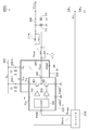
- FIG. 1 is a circuit diagram showing a configuration example of a multi-phase step-down DC / DC converter.
- the DC / DC converter 200 is composed of N phases (N ⁇ 2), and has an input line 202, an output line 204, N inductors L1_1 to L1_N, an input capacitor Ci, an output capacitor Co, a controller 210, and N power modules. 220_1 to 220_N.
- a load (not shown) whose power consumption (load current I OUT ) dynamically changes is connected to the output line 204.
- the DC / DC converter 200 receives the input voltage V IN of the input line 202, generates an output voltage V OUT stabilized at a predetermined level, and supplies the output voltage V OUT to a load.
- An input capacitor Ci for stabilizing the input voltage V IN is connected to the input line 202, and an output capacitor Co for smoothing the output voltage V OUT is connected to the output line 204.
- the power module 220 mainly includes a VIN pin, a PGND pin, a SW pin, a VCC pin, an AGND pin, and a PWM pin.
- the power module 220 includes a high side switch (switching transistor) M1 provided between the VIN pin and the SW pin, a low side switch (synchronous rectification transistor transistor) M2 provided between the SW pin and the PGND pin, and a high side driver 222. , A low side driver 224 and a logic circuit 226.
- the controller 210 receives the feedback signal V FB according to the output voltage V OUT , and generates the pulse signal S PWM whose duty ratio is adjusted so that the feedback signal V FB approaches the predetermined target voltage V REF , and N
- the power modules 220_1 to 220_N are distributed to K power modules.
- the pulse signals S PWM1 to S PWMK having a phase difference of (360 / K) degrees are distributed to the K power modules 220_1 to 220_K.
- the components of the DC / DC converter 200 are mounted on a printed circuit board.
- the inductors L1_1 to L1_N and the power modules 220_1 to 220_N which are the main components, are mounted on the same mounting surface.
- the main constituent parts mentioned here are parts having a large occupied area and large current flows.
- the area occupied by the DC / DC converter 200 increases. This means that the area of the printed circuit board becomes large, which may be a factor in increasing the cost.
- the heat generation of the power modules 220_1 to 220_N is large, it is necessary to cool the power modules 220_1 to 220_N with a heat sink.
- the plurality of power modules 220_1 to 220_N are arranged close to other components such as the plurality of inductors L1_1 to L1_N, the shape of the heat sink may be restricted by the other components and the cooling effect may be sacrificed.
- the present invention has been made in view of the above problems, and one of exemplary purposes of a certain aspect thereof is to provide a power supply device capable of solving at least one of the above problems.
- the power supply device includes an input line to which a DC input voltage is supplied, an output line to which a load is connected, an output capacitor connected to the output line, and N inductors associated with N phases, Of N inductors, one end of which is connected to the output line, and N power modules (also referred to as power stage modules) associated with N phases, each of which is an input pin connected to the input line, N power modules each having a switching pin connected to the other end of the corresponding inductor and a ground pin grounded. At least one of the N power modules is mounted on the sub-mounting surface of the printed circuit board opposite to the main mounting surface.
- FIG. 3A is a layout diagram of the back surface electrode of the power module
- FIG. 3B is a layout diagram of the back surface electrode of the inductor.
- FIGS. 6A and 6B are layout diagrams of the DC / DC converter according to the example 1-1.
- FIG. 6A and 6B are layout diagrams of the DC / DC converter according to the example 1-1.
- FIG. 6 is a diagram showing a wiring pattern of a DC / DC converter according to an example 1-1. It is the perspective view which looked at a DC / DC converter from the sub-mounting surface SB side.
- 9A and 9B are cross-sectional views of the heat sink according to the first configuration example.
- 10A and 10B are cross-sectional views of the heat sink according to the second configuration example.
- 11A and 11B are layout diagrams of the DC / DC converter according to the embodiment 1-2.
- FIG. 6 is a diagram showing a wiring pattern of a DC / DC converter according to Example 1-2.
- FIGS. 13A and 13B are layout diagrams of the DC / DC converter according to the example 1-3.
- 14A and 14B are layout diagrams of the DC / DC converter according to the example 1-4.
- FIG. 7 is an equivalent circuit diagram of a DC / DC converter according to a second embodiment.
- 16A and 16B are layout diagrams of the DC / DC converter according to the embodiment 2-1.
- FIG. 6 is a diagram showing a wiring pattern of a DC / DC converter according to an example 2-1.
- 18A and 18B are layout diagrams of the DC / DC converter according to the embodiment 2-2.
- 19A and 19B are layout diagrams of the DC / DC converter according to the example 2-3.
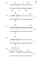
- 20A to 20E are cross-sectional views illustrating the assembly process of the electronic device.
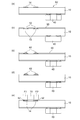
- 21A to 21E are cross-sectional views illustrating the assembly process of the electronic device.
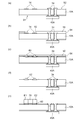
- 22 (a) to 22 (e) are diagrams for explaining component mounting on the first surface S1, and FIGS.
- FIGS. 23A to 23E are views for explaining component mounting on the second surface S2. is there.
- FIGS. 23A to 23E are views for explaining component mounting on the second surface S2.
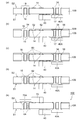
- 24A to 24E are views for explaining the method for manufacturing the electronic device according to the embodiment.
- 25A to 25E are views for explaining the method for manufacturing the electronic device according to the embodiment.
- the power supply device includes an input line to which a DC input voltage is supplied, an output line to which a load is connected, an output capacitor connected to the output line, N inductors associated with N phases, and N inductors. And a power module.
- each of the N inductors is connected to the output line.
- the N power modules are associated with the N inductors, and each has an input pin connected to the input line, a switching pin connected to the other end of the corresponding inductor, and a ground pin grounded. . At least one of the N power modules is mounted on the sub-mounting surface of the printed circuit board opposite to the main mounting surface.
- All N power modules may be mounted on the sub-mounting surface.
- the power supply device may include a heat sink that commonly contacts the upper surfaces of the N power modules.
- the N power modules may be mounted alternately on the main mounting surface and the sub mounting surface. Thereby, the heat generated by the plurality of power modules can be dispersed on both sides of the printed circuit board. In addition, since the space between adjacent power modules on the same mounting surface doubles, thermal concentration can be relaxed.
- the N power modules are paired with the first, second, third, fourth, ..., And the two power modules forming a pair may be connected to a common input line.
- the capacitors connected to the input lines can be shared in two phases, and the number of parts can be reduced. Alternatively, if the same number of capacitors are used, the effect of the capacitors can be doubled.
- the state in which the member A is connected to the member B means that the members A and B are electrically connected in addition to the case where the members A and B are physically directly connected. It also includes the case of being indirectly connected via another member that does not substantially affect the general connection state or does not impair the function or effect achieved by their connection.
- the state in which the member C is provided between the member A and the member B means that the members A and C or the members B and C are directly connected to each other and their electrical It also includes the case of being indirectly connected via another member that does not substantially affect the general connection state or does not impair the function or effect achieved by their connection.
- One aspect of the present invention is understood as a layout or mounting technique of a DC / DC converter.
- the function or equivalent circuit of the DC / DC converter is the same as in FIG.
- a power module 220 common to some embodiments will be described.
- the power module 220 itself is publicly known and is manufactured and sold by various IC makers.
- the circuit configuration of the power module 220 is similar to that of FIG. 1, and includes a high side transistor M1, a low side transistor M2, a high side driver 222, a low side driver 224, and a logic circuit 226.
- the power module 220 also includes an input (VIN) pin, a switching pin (SW), a ground pin (PGND, AGND), a power supply (VCC) pin, a control (PWM) pin, and the like.
- the power module 220 includes a bootstrap circuit, various protection circuits, and a plurality of pins related to the bootstrap circuit and the like.
- the power supply voltage V CC is supplied to each circuit block including the logic circuit 226 via the VCC pin.
- the AGND pin is the ground for the high side driver 222, the low side driver 224, the logic circuit 226, and the like.
- the direct current input voltage V IN is supplied to the VIN pin, and the PGND pin is the ground of the output stage.
- the logic circuit 226 generates a high side pulse and a low side pulse according to the PWM signal S PWM input to the PWM pin.
- the high-side driver 222 drives the high-side transistor M1 based on the high-side pulse
- the low-side driver 224 drives the low-side transistor M2 based on the low-side pulse.
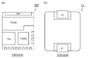
- FIG. 3A is a layout diagram of the back surface electrode of the power module 220.
- the power module 220 includes the VIN pin, the PGND pin, the SW pin, the VCC pin, and the AGND pin.
- the VIN pin and the GND pin are relatively larger in area than other pads.
- the PGND pin and the AGND pin also have a function as a thermal pad, they have a large area.
- the PWM pin and other control pins are assigned to the remaining pins.
- the layout of the back surface electrode in FIG. 3 is merely an example, and it goes without saying that it differs depending on the chip vendor and the product.
- FIG. 3B is a layout diagram of the back surface electrode of the inductor L1.
- the inductor L1 has a first electrode E1 and a second electrode E2 arranged in the center of two opposite sides.
- One of the problems to be solved in this embodiment is improvement of layout. Therefore, first, a layout serving as a reference for comparison (hereinafter referred to as a comparison technique) will be described.
- Recent electronic circuits are mounted using surface mounting technology (SDT: Surface Mount Technology).
- SDT Surface Mount Technology
- cream solder is applied to pads (lands) formed on a printed circuit board, components are mounted using a mounter, and reflow processing is performed.
- the DC / DC converter is no exception, and therefore, in the comparative technique, basically all components are mounted on the main mounting surface.
- FIG. 4 is a layout diagram of a DC / DC converter according to the comparative technique.
- N 3.
- the controller 210, the power modules 220_1 to 220_N, the input capacitor Ci, and the output capacitor Co (referred to as main components) are all laid out on the main mounting surface SA of the printed circuit board 300R.
- the plurality of inductors L1_1 to L1_N are arranged side by side in the first direction (x direction) on the printed circuit board.
- FIG. 5 is a diagram showing a wiring pattern of a printed circuit board 300R according to the comparative technique.
- circles indicate via holes.
- a plurality of pattern wirings (printed wirings) PTN1_1 to PTN1_3, PTN_2, PTN3_1 to PTN3_3, PTN4 are formed on the printed circuit board 300.
- the first pattern wirings PTN1_1 to PTN1_3 correspond to the input lines 202_1 to 202_3 of FIG.
- the second pattern wiring PTN2 is a ground plane and is formed commonly for all phases in order to minimize impedance.
- An input capacitor Ci_ # is provided between the first pattern wiring PTN1_ # and the second pattern wiring PTN2.
- the input capacitor Ci_ # may be an MLCC (multilayer ceramic capacitor), an electrolytic capacitor, or a combination thereof.
- Third pattern wirings PTN3_1 to PTN3_3 are wirings that connect the SW pin of the power module 220 and one end of the inductor L1 in FIG.
- the fourth pattern wiring PTN4 corresponds to the output line 204 in FIG.
- the output capacitor Co (not shown in FIG. 5) of FIG. 1 is connected between the fourth pattern wiring PTN4 and the ground plane.
- each of these pattern wirings PTN1 to PTN4 forms a multilayer wiring and is connected to a wiring of another wiring layer not shown in FIG. 5 via a via hole.
- the layout according to the embodiment will be described.
- at least one of the N power modules 220 is mounted on the sub-mounting surface SB of the printed circuit board 300 opposite to the main mounting surface SA.
- some examples will be described.
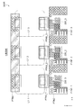
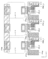
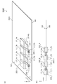
- Example 1-1) 6A and 6B are layout diagrams of the DC / DC converter 200A according to the embodiment 1-1.
- FIG. 6A is a perspective view and FIG. 6B is a sectional view.
- all the power modules 220_1 to 220_3 are mounted on the sub mounting surface SB.
- the input capacitor Ci_ # is preferably connected in the immediate vicinity of the VIN pin of the power module 220_ #. Therefore, in the example 1-1, the input capacitor Ci_ # is also mounted on the sub mounting surface SB.
- FIG. 7 is a diagram showing a wiring pattern of the DC / DC converter 200A according to the embodiment 1-1.
- components mounted on the main mounting surface SA side are indicated by broken lines, and components mounted on the sub mounting surface SB side are indicated by chain double-dashed lines.
- the functions of the pattern wirings PTN1 to PTN4 are the same as in FIG.
- the pattern wirings PTN1 to PTN4 are multilayer wirings and are formed so as to overlap both surfaces (and intermediate wiring layers) of the main mounting surface SA and the sub mounting surface SB, and they are electrically connected to each other by via holes. .
- the above is the configuration of the DC / DC converter 200A according to the embodiment 1-1.
- a space margin is generated on the main mounting surface SA or the sub-mounting surface SB. The advantage of this will be described.
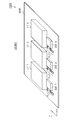
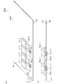
- FIG. 8 is a perspective view of the DC / DC converter 200A as viewed from the sub-mounting surface SB side.
- the DC / DC converter 200A includes a heat sink 240.
- the heat sink 240 is in contact with the upper surfaces of the plurality of power modules 220_1 to 220_3 in common.
- On the side of the sub-mounting surface SB since there are no components taller than the power module 220 around the power modules 220_1 to 220_N, a large heat sink 240 can be provided and cooling efficiency can be improved.
- FIG. 9A and 9B are cross-sectional views of the heat sink 240A according to the first configuration example.
- FIG. 9A shows a state where the heat sink 240A is applied to the example 1-1
- FIG. 9B shows a state where the same heat sink 240A is applied to the comparative technique of FIG.
- the heat sink 240A has a heat radiating portion 242 and a contact portion 244. An opening is provided in the heat dissipation portion 242, and a contact portion 244 is fitted in this opening. The contact portion 244 contacts the power module 220 to be cooled.
- Example 1-1 in which the power module 220 is mounted on the sub-mounting surface SB, there is no tall component around the power module 220 as shown in FIG.
- the portion 242 can be brought closer to the printed circuit board surface.
- the height of the contact portion 244 in the Z direction can be reduced. This can reduce the thermal resistance and improve the cooling performance.
- FIGS. 10A and 10B are cross-sectional views of the heat sink 240B according to the second configuration example.
- the heat sink 240B is composed of a single heat radiating plate 246 and is provided with a convex portion 248 by drawing.
- the heat radiating plate 246 is in contact with the surface of the power module 220 at the convex portion 248.
- the heat sink 240B in FIG. 10 has a simplified structure as compared with the heat sink 240A in FIG. 9, so the cost can be reduced. Further, since no opening is required, the electromagnetic noise shielding performance is high and the EMC (Electro Magnetic Compatibility) can be improved.
- EMC Electro Magnetic Compatibility
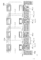
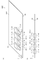
- 11A and 11B are layout diagrams of the DC / DC converter 200B according to the embodiment 1-2.
- 11A is a perspective view and FIG. 11B is a sectional view.
- the N power modules 220_1 to 220_N are mounted alternately on the main mounting surface SA and the sub mounting surface SB.
- FIG. 12 is a diagram showing a wiring pattern of the DC / DC converter 200B according to the embodiment 1-2.
- components mounted on the main mounting surface SA side are indicated by broken lines, and components mounted on the sub mounting surface SB side are indicated by chain double-dashed lines.
- the functions of the pattern wirings PTN1 to PTN4 are as described above.
- the pattern wirings PTN1 to PTN4 are multilayer wirings and are formed so as to overlap both surfaces (and intermediate wiring layers) of the main mounting surface SA and the sub mounting surface SB, and they are electrically connected to each other by via holes. .
- Example 1-2 the N power modules are paired with the first, second, third, fourth, ...
- the two power modules 220_i and 220_j forming a pair are connected to a common input line (that is, a common first pattern wiring PTN1_i, j).
- the input capacitors Ci_i, j can also be made common. That is, the input capacitor Ci_i, j on the main mounting surface SA side functions as an input capacitor of the power module 220_i, and at the same time, functions as an input capacitor of the power module 220_j on the sub mounting surface SB side, so that the effect of the input capacitor is doubled. can do. Alternatively, the number of capacitors required to obtain the same effect of the input capacitors can be reduced, and the cost can be reduced.
- Example 1-3 13A and 13B are layout diagrams of the DC / DC converter 200D according to the example 1-3.
- the chip size of the inductor of Example 1-2 is reduced.
- a component with a small allowable current, that is, a small chip size can be selected, and the occupied area can be reduced.
- Example 1-4 14A and 14B are layout diagrams of the DC / DC converter 200G according to the first to fourth embodiments.
- Example 1-4 is a modification of Example 1-3 in the layout of the inductors. Specifically, each inductor L1_i is mounted on the same surface as the corresponding power module 220_i. As a result, the corresponding inductor L1_i and power module 220_i can be connected with low impedance.
- the pair of inductors L1_1 and L1_2 is mounted so as to overlap both surfaces SA and SB of the printed circuit board 300G.
- the pair of inductors L1_3 and L1_4 is mounted so as to overlap both surfaces SA and SB of the printed circuit board 300G.
- the chip size can be reduced in an application in which the coil current flowing through the inductor L1 is small.
- the coil current flowing through the inductor L1 is large, it is inevitable to select a component having a large allowable current and thus a large chip size, and the occupied size of the DC / DC converter is restricted by the chip size of the inductor.
- the second embodiment will explain a technique of reducing the occupied size of the DC / DC converter in an application where the coil current is large.
- FIG. 15 is an equivalent circuit diagram of the DC / DC converter 200C according to the second embodiment.
- the inductance value of the inductor chip in the case of two parallels is 1/2 times that in the case of a single inductor chip.
- the amount of current flowing through the inductor chip is 1/2 times that in the case of a single inductor chip.
- the second embodiment by reducing the amount of current per chip, it is possible to select an inductor chip with a small current capacity and therefore a small package size. For example, in the case of adopting a 10 mm square inductor chip in the case of a single inductor chip, the technical idea of the second embodiment is introduced, and by adopting two parallels, a 6 mm square inductor chip is adopted. You can
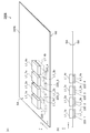
- Example 2-1 16A and 16B are layout diagrams of the DC / DC converter 200C according to the embodiment 2-1. 16 (a) is a perspective view and FIG. 16 (b) is a sectional view.
- the two inductor chips L1_ # a and L1_ # b electrically connected in parallel are mounted on the main mounting surface SA and the sub mounting surface SB of the printed circuit board 300C so as to overlap each other.
- Example 2-1 the N power modules 220_1 to 220_N are mounted on the main mounting surface SA and the sub mounting surface SB alternately, as in Example 1-2 of the first embodiment.
- FIG. 17 is a diagram showing a wiring pattern of the DC / DC converter 200C according to the embodiment 2-1.
- Example 2-1 the same effect as that of Example 1-2 can be obtained. That is, the input lines can be shared by the adjacent two phases, and the input capacitors Ci_i, j can also be shared.
- Example 2-2 18A and 18B are layout diagrams of the DC / DC converter 200E according to the embodiment 2-2.
- 18A is a perspective view and FIG. 18B is a sectional view.
- the example 2-2 is common to the example 1-1 of FIG. 6 in that a plurality of power modules 220_1 to 220_4 are mounted on the sub mounting surface SB.
- the input capacitor Ci is omitted in FIG. 18, it may be mounted on the sub-mounting surface SB as in Example 1-1.
- the area occupied by the DC / DC converter 200E can be reduced, as in the embodiment 2-1.
- FIG. 19A and 19B are layout diagrams of the DC / DC converter 200F according to the embodiment 2-3.
- 19 (a) is a perspective view
- FIG. 19 (b) is a sectional view.
- the plurality of power modules 220_1 to 220_4 are all mounted on the main mounting surface SA side.
- the area occupied by the DC / DC converter 200F can be reduced.
- the inductor L1 for each phase is formed by connecting two inductor chips in parallel, but the number of chips is not limited to two, and may be three or more.
- the inductor component and the resistance component of the input line 202 are as small as possible. Further, it is desirable that the PGND pin is also grounded with the smallest possible impedance.
- a pad (land) for soldering the VIN pin is formed on the first pattern wiring PTN1, and a PGND pin is soldered on the second pattern wiring PTN2. Pad (land) is formed.
- a multilayer wiring is adopted and a large number of via holes are provided. To reduce the impedance as much as possible, it is necessary to form the via holes inside the pads (lands). To be done. Such a via hole is called an in-pad via.
- Electronic equipment includes a printed circuit board and electronic components mounted on the printed circuit board.
- surface mount devices SMD: Surface Mount Device
- chip inductors, chip resistors, chip capacitors, and transistors have become mainstream.
- FIG. 20A shows the printed circuit board 10 before components are mounted.
- Printed wiring (not shown) and pads (lands) 12 and 14 are formed on the first surface (leading mounting surface) S1 and the second surface S2 (backward mounting surface) of the printed circuit board 10.
- the pads 12 and 14 are arranged at locations corresponding to the electrodes of the component, and the portions other than the pads 12 and 14 are covered with the resist 11.
- a screen also referred to as a metal mask or a solder mask
- An opening 22 is provided in the screen 20 at a position overlapping the pad 12 on the first surface S1 side.
- cream solder (solder paste) 30 is applied from above the screen 20.
- the screen 20 is removed as shown in FIG. 20D, the cream solder 32 remains only on the pad 12.
- the component 40 is mounted on the first surface S1 by the mounter.
- the cream solder 32 is sandwiched between the pads 12 and the electrodes E1 and E2 of the component 40.
- the reflow process is performed to electrically and mechanically connect the component 40 and the substrate 10.
- the printed circuit board 10 is inverted so that the second surface S2 is on the upper side.
- the screen 50 is placed on the second surface S2.
- An opening 52 is provided in the screen 50 at a position overlapping the pad 14 on the second surface S2 side.
- cream solder 60 is applied from above the screen 50.
- the screen 50 is removed as shown in FIG. 21D, the cream solder 62 remains only on the pad 14.
- the component 70 is mounted on the second surface S2 by the mounter.
- the cream solder 62 is sandwiched between the electrodes E1 and E2 of the component 70 and the pad 14.
- the reflow process is performed to electrically and mechanically connect the component 70 and the substrate 10.
- the printed circuit board 10 includes a plurality of wiring layers, and the different wiring layers are connected via vias.
- the vias are usually arranged so as to avoid the positions of the pads, but they may be arranged in the pads when it is desired to enhance heat dissipation or reduce parasitic impedance.
- the via arranged in the pad is called an in-pad via.
- FIGS. 23 (a) to 23 (e) are diagrams for explaining component mounting on the second surface S2. is there.
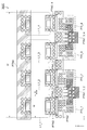
- a pad (land) 16 and a via 17 in the pad are formed on the first surface (preceding mounting surface) S1 of the printed circuit board 10A.
- the screen 20 is placed on the first surface S1 (FIG. 22 (b)), and then the cream solder 30 is applied from above the screen 20 (FIG. 22 (c)). When the screen 20 is removed, the cream solder 32 remains on the pad 16 (FIG. 22 (d)).
- the component 40A is mounted on the first surface S1 by the mounter (FIG. 22 (e)).
- the component 40A has a back surface electrode E3, and the cream solder 32 is sandwiched between the back surface electrode E3 and the pad 16.
- reflow processing is performed, and the component 40A and the substrate 10 are electrically and mechanically connected.
- part of the cream solder 32 penetrates the via 17 in the pad (through hole) and leaks from the second surface S2 side.
- the solder leak 34 causes a mounting failure as described below.
- FIGS. 23 (a) to 23 (e) the printed circuit board 10A is inverted so that the second surface S2 is on the upper side. Subsequently, as shown in FIG. 23B, the screen 50 is placed on the second surface S2. The screen 50 has an opening 52 where it overlaps with the pad 14.
- FIG. 23C shows a state in which the screen 50 is removed.
- the cream solder 62 is applied to an unintended area other than the pad 14.
- Another approach is to fill the inside of the via hole with metal or resin in advance in the manufacturing process of the printed circuit board 10A to close the hole. According to this measure, it is possible to prevent the cream solder 30 from leaking to the second surface S2 side in the process of FIG. However, in this solution, the number of manufacturing steps of the printed circuit board 10A increases, so that the cost of the printed circuit board 10A increases.
- FIGS. 24 (a) to (e) and FIGS. 25 (a) to (e) are diagrams for explaining the method for manufacturing the electronic device according to the embodiment. 24 (a) to (e) and FIGS. 25 (a) to (e) show an assembly process by surface mounting.
- the component mounting on the first surface S1 will be described with reference to FIGS. 24 (a) to 24 (e).
- the mounting on the first surface S1 is substantially the same as that of FIG. 22 as described below.
- FIG. 24A shows the printed circuit board 10B before components are mounted.
- Several pads (lands) 12 and 16 are formed on the first surface (preceding mounting surface) S1 of the printed circuit board 10B.
- An in-pad via 17 is formed in the pad 16.
- Several pads 14 and 18 are similarly formed on the second surface (subsequent mounting surface) S2 of the printed circuit board 10B. Vias 19 in the pad are formed in the pad 18.
- the screen 20 is placed on the first surface S1.
- the screen 20 is provided with openings 22 and 24 at positions corresponding to the pads 12 and 16. Subsequently, the cream solder 30 is applied from above the screen 20 (FIG. 24C).
- the components 40 and 40A are mounted on the first surface S1 by the mounter (FIG. 24 (e)).
- the cream solder 32 is sandwiched between the pads 12 and the electrodes E1 and E2 of the component 40.
- the component 40A has a back surface electrode E3, and the cream solder 32 is sandwiched between the back surface electrode E3 and the pad 16. In this state, reflow processing is performed, and the component 40A and the substrate 10 are electrically and mechanically connected.
- part of the cream solder 32 penetrates the pad via 17 (through hole) and leaks from the second surface S2 side.
- FIGS. 25 (a) to 25 (e) component mounting on the second surface S2 will be described with reference to FIGS. 25 (a) to 25 (e).
- the printed circuit board 10B is inverted so that the second surface S2 is on the upper side.
- the screen 50B is placed on the second surface S2.
- the screen 50B has an opening 52 at a position overlapping the pad 14.
- the screen 50 ⁇ / b> B is provided with a recess 56 at a position overlapping the via 19 in the pad. The recess 56 prevents the screen 50B from interfering with the solder leak 34, and allows the screen 50B to be in close contact with the second surface S2.
- FIG. 25D shows a state in which the screen 50B is removed.
- the cream solder 62 is applied only on the pads 14 and 18, and an excessive protrusion is suppressed.
- the components 70 and 70A are mounted on the second surface S2 and subjected to reflow processing.
- the electrodes E1 and E2 are electrically and mechanically connected to the pad 14.
- the back surface electrode E3 and the pad 18 are electrically and mechanically connected to each other, and the semiconductor device 100 is assembled.
- the above is the method for manufacturing the semiconductor device according to the embodiment.
- the screen 50 used for applying the cream solder to the second surface S2 is provided with the concave portion 56 for avoiding interference with the solder leak 34. This can prevent the screen 50B from being displaced due to the solder leak 34, and can prevent the cream solder 60 from entering the gap between the screen 50B and the second surface S2.
- solder leakage 64 may occur from the via 19 in the pad to the first surface S1 side, but the mounting of the component on the first surface S1 side is completed. Therefore, there is no adverse effect.
- the present invention relates to a power supply device.
Landscapes
- Engineering & Computer Science (AREA)
- Power Engineering (AREA)
- Dc-Dc Converters (AREA)
Priority Applications (3)
| Application Number | Priority Date | Filing Date | Title |
|---|---|---|---|
| EP19872843.8A EP3869678A4 (en) | 2018-10-19 | 2019-10-18 | POWER SOURCE DEVICE |
| CN201980067237.2A CN112868170A (zh) | 2018-10-19 | 2019-10-18 | 电源装置 |
| US17/283,723 US12009750B2 (en) | 2018-10-19 | 2019-10-18 | Power source device |
Applications Claiming Priority (2)
| Application Number | Priority Date | Filing Date | Title |
|---|---|---|---|
| JP2018-197715 | 2018-10-19 | ||
| JP2018197715A JP7250474B2 (ja) | 2018-10-19 | 2018-10-19 | 電源装置 |
Publications (1)
| Publication Number | Publication Date |
|---|---|
| WO2020080526A1 true WO2020080526A1 (ja) | 2020-04-23 |
Family
ID=70283040
Family Applications (1)
| Application Number | Title | Priority Date | Filing Date |
|---|---|---|---|
| PCT/JP2019/041098 Ceased WO2020080526A1 (ja) | 2018-10-19 | 2019-10-18 | 電源装置 |
Country Status (5)
| Country | Link |
|---|---|
| US (1) | US12009750B2 (enExample) |
| EP (1) | EP3869678A4 (enExample) |
| JP (2) | JP7250474B2 (enExample) |
| CN (1) | CN112868170A (enExample) |
| WO (1) | WO2020080526A1 (enExample) |
Families Citing this family (2)
| Publication number | Priority date | Publication date | Assignee | Title |
|---|---|---|---|---|
| CN116471807A (zh) * | 2022-08-01 | 2023-07-21 | 成都芯源系统有限公司 | 一种具有夹层结构的电源模块 |
| CN119653587B (zh) * | 2024-12-17 | 2026-06-16 | 蔚来汽车科技(安徽)有限公司 | 嵌入式印刷电路板布局结构以及电子设备 |
Citations (6)
| Publication number | Priority date | Publication date | Assignee | Title |
|---|---|---|---|---|
| US20090108821A1 (en) * | 2007-03-07 | 2009-04-30 | Martin Standing | Multi-phase voltage regulation module |
| JP2009159704A (ja) * | 2007-12-26 | 2009-07-16 | Keihin Corp | パワードライブユニット |
| JP2010124570A (ja) * | 2008-11-18 | 2010-06-03 | Toshiba Carrier Corp | 電力変換装置 |
| JP2016067164A (ja) * | 2014-09-25 | 2016-04-28 | 株式会社ノーリツ | パワーコンディショナ |
| JP2017112147A (ja) * | 2015-12-14 | 2017-06-22 | 株式会社小糸製作所 | 発光モジュール、灯具および発光素子用回路基板 |
| CN207573821U (zh) * | 2017-12-14 | 2018-07-03 | 苏州众能医疗科技有限公司 | 一种双面水冷板散热装置 |
Family Cites Families (36)
| Publication number | Priority date | Publication date | Assignee | Title |
|---|---|---|---|---|
| US4761881A (en) | 1986-09-15 | 1988-08-09 | International Business Machines Corporation | Single step solder process |
| US4739919A (en) | 1987-06-15 | 1988-04-26 | Northern Telecom Limited | Masking of circuit boards for wave soldering |
| JP2502663B2 (ja) | 1988-03-17 | 1996-05-29 | 松下電器産業株式会社 | プリント配線板の製造方法 |
| US5144535A (en) * | 1989-04-20 | 1992-09-01 | U.S. Philips Corporation | Method of mounting electrical and/or electronic components of a printed circuit board |
| JPH0357295A (ja) | 1989-07-26 | 1991-03-12 | Fujitsu Ltd | 両面実装プリント板への電子部品実装方法 |
| US5155904A (en) * | 1991-04-03 | 1992-10-20 | Compaq Computer Corporation | Reflow and wave soldering techniques for bottom side components |
| JPH06334323A (ja) | 1993-05-25 | 1994-12-02 | Sony Corp | はんだプリコート方法 |
| JPH0794619A (ja) * | 1993-09-20 | 1995-04-07 | Hitachi Ltd | 混成集積回路装置 |
| US5373984A (en) | 1993-09-27 | 1994-12-20 | Sundstrand Corporation | Reflow process for mixed technology on a printed wiring board |
| JP2001068833A (ja) | 1999-08-27 | 2001-03-16 | Minami Kk | 部品実装済基板への接着剤の塗布方法 |
| CN1250056C (zh) | 2002-12-05 | 2006-04-05 | 华为技术有限公司 | 一种加工印制电路板的方法 |
| US7350175B2 (en) * | 2004-09-29 | 2008-03-25 | Matsushita Electric Industrial Co., Ltd. | Circuit board design system, design data analysis method and recording medium with analysis program recorded thereon |
| JP5142119B2 (ja) * | 2006-09-20 | 2013-02-13 | 住友電装株式会社 | 放熱構造を備えたプリント基板の製造方法および該方法で製造されたプリント基板の放熱構造 |
| TW200906254A (en) | 2007-07-18 | 2009-02-01 | Universal Scient Ind Co Ltd | Method for a unitary plate coated with different solder-pastes and its mold-plate set |
| JP5420433B2 (ja) * | 2010-01-14 | 2014-02-19 | ルネサスエレクトロニクス株式会社 | 半導体装置および電源装置 |
| JP2013162585A (ja) * | 2012-02-02 | 2013-08-19 | Sony Computer Entertainment Inc | Dc/dcコンバータ |
| JP5974603B2 (ja) * | 2012-04-17 | 2016-08-23 | 株式会社村田製作所 | インダクタアレイチップ及びdc−dcコンバータ |
| JP6034132B2 (ja) * | 2012-10-24 | 2016-11-30 | 株式会社ソニー・インタラクティブエンタテインメント | Dc/dcコンバータおよびそれを用いたゲーム機器 |
| JP6162510B2 (ja) | 2013-07-03 | 2017-07-12 | 株式会社ソニー・インタラクティブエンタテインメント | 降圧dc/dcコンバータ、そのコントローラおよび制御方法、ならびにそれを用いた電子機器 |
| JP6261071B2 (ja) | 2013-10-15 | 2018-01-17 | オムロンオートモーティブエレクトロニクス株式会社 | コイル一体型プリント基板、磁気デバイス |
| US9564389B2 (en) * | 2014-03-18 | 2017-02-07 | Infineon Technologies Americas Corp. | Semiconductor package with integrated die paddles for power stage |
| JP6106127B2 (ja) * | 2014-05-29 | 2017-03-29 | 株式会社ソニー・インタラクティブエンタテインメント | スイッチングコンバータおよびそれを用いた電子機器 |
| US20160105983A1 (en) * | 2014-10-09 | 2016-04-14 | International Rectifier Corporation | Insertable Power Unit with Mounting Contacts for Plugging into a Mother Board |
| DE102015200716A1 (de) * | 2015-01-19 | 2016-07-21 | Efficient Energy Gmbh | Schaltnetzteil |
| CN111952293B (zh) * | 2019-05-15 | 2022-07-01 | 台达电子企业管理(上海)有限公司 | 功率模块及其制造方法 |
| US12058814B2 (en) * | 2016-03-03 | 2024-08-06 | Delta Electronics (Shanghai) Co., Ltd. | Power module and manufacturing method thereof |
| JP6603411B2 (ja) * | 2016-06-07 | 2019-11-06 | 株式会社ソニー・インタラクティブエンタテインメント | Dc/dcコンバータおよび電子機器 |
| US10063149B2 (en) * | 2016-11-23 | 2018-08-28 | Apple Inc. | Multi-phase switching power converter module stack |
| US10671009B2 (en) | 2017-02-13 | 2020-06-02 | Canon Kabushiki Kaisha | Printed circuit board mounting piezoelectric transformer |
| US10361631B2 (en) | 2017-10-05 | 2019-07-23 | Monolithic Power Systems, Inc. | Symmetrical power stages for high power integrated circuits |
| US10505456B1 (en) * | 2018-09-07 | 2019-12-10 | International Business Machines Corporation | Fully integrated multi-phase buck converter with coupled air core inductors |
| JP6835788B2 (ja) * | 2018-10-19 | 2021-02-24 | 株式会社ソニー・インタラクティブエンタテインメント | 電源装置 |
| JP7107810B2 (ja) * | 2018-10-19 | 2022-07-27 | 株式会社ソニー・インタラクティブエンタテインメント | 半導体装置の製造方法およびスクリーン |
| CN209517580U (zh) * | 2018-12-21 | 2019-10-18 | 苏州纽克斯电源技术股份有限公司 | 一种电源 |
| CN112448561B (zh) * | 2019-08-30 | 2022-04-15 | 台达电子企业管理(上海)有限公司 | 电源模块及电源模块的制备方法 |
| CN112788842B (zh) * | 2019-11-08 | 2025-04-08 | 华为技术有限公司 | 一种芯片供电系统、芯片、pcb和计算机设备 |
-
2018
- 2018-10-19 JP JP2018197715A patent/JP7250474B2/ja active Active
-
2019
- 2019-10-18 CN CN201980067237.2A patent/CN112868170A/zh active Pending
- 2019-10-18 WO PCT/JP2019/041098 patent/WO2020080526A1/ja not_active Ceased
- 2019-10-18 EP EP19872843.8A patent/EP3869678A4/en active Pending
- 2019-10-18 US US17/283,723 patent/US12009750B2/en active Active
-
2021
- 2021-08-30 JP JP2021139859A patent/JP7250866B2/ja active Active
Patent Citations (6)
| Publication number | Priority date | Publication date | Assignee | Title |
|---|---|---|---|---|
| US20090108821A1 (en) * | 2007-03-07 | 2009-04-30 | Martin Standing | Multi-phase voltage regulation module |
| JP2009159704A (ja) * | 2007-12-26 | 2009-07-16 | Keihin Corp | パワードライブユニット |
| JP2010124570A (ja) * | 2008-11-18 | 2010-06-03 | Toshiba Carrier Corp | 電力変換装置 |
| JP2016067164A (ja) * | 2014-09-25 | 2016-04-28 | 株式会社ノーリツ | パワーコンディショナ |
| JP2017112147A (ja) * | 2015-12-14 | 2017-06-22 | 株式会社小糸製作所 | 発光モジュール、灯具および発光素子用回路基板 |
| CN207573821U (zh) * | 2017-12-14 | 2018-07-03 | 苏州众能医疗科技有限公司 | 一种双面水冷板散热装置 |
Non-Patent Citations (1)
| Title |
|---|
| See also references of EP3869678A4 * |
Also Published As
| Publication number | Publication date |
|---|---|
| JP2021185740A (ja) | 2021-12-09 |
| JP7250866B2 (ja) | 2023-04-03 |
| US12009750B2 (en) | 2024-06-11 |
| US20210328515A1 (en) | 2021-10-21 |
| JP2020065427A (ja) | 2020-04-23 |
| JP7250474B2 (ja) | 2023-04-03 |
| EP3869678A4 (en) | 2022-07-06 |
| EP3869678A1 (en) | 2021-08-25 |
| CN112868170A (zh) | 2021-05-28 |
Similar Documents
| Publication | Publication Date | Title |
|---|---|---|
| JP6835788B2 (ja) | 電源装置 | |
| JP7107810B2 (ja) | 半導体装置の製造方法およびスクリーン | |
| US20230230749A1 (en) | Power system | |
| JP4953034B2 (ja) | 電圧変換器 | |
| US6940724B2 (en) | DC-DC converter implemented in a land grid array package | |
| KR101301476B1 (ko) | 집적 인덕터를 포함하는 장치, 시스템 및 파워 컨버터 | |
| US20230282569A1 (en) | Power supply circuit module | |
| KR20080087161A (ko) | 오픈 프레임 패키지를 가지는 하이 파워 모듈 | |
| CN112788842A (zh) | 一种芯片供电系统、芯片、pcb和计算机设备 | |
| TW201728240A (zh) | 堆疊電子結構 | |
| TWI893418B (zh) | 印刷電路板和包括印刷電路板的電子設備 | |
| US7721232B2 (en) | Designated MOSFET and driver design to achieve lowest parasitics in discrete circuits | |
| JP7250866B2 (ja) | 電源装置 | |
| JP5190811B2 (ja) | 電源モジュール | |
| JP6759874B2 (ja) | 電力変換装置 | |
| US20090154112A1 (en) | Packaging structure of power module | |
| US20220336138A1 (en) | Magnetic device and power conversion module | |
| JP2009044029A (ja) | 複数マイコン実装回路装置 | |
| JP2024180042A (ja) | 電力変換装置 | |
| JP2024117301A (ja) | 電力変換装置 | |
| CN120568582A (zh) | 一种电路板 |
Legal Events
| Date | Code | Title | Description |
|---|---|---|---|
| 121 | Ep: the epo has been informed by wipo that ep was designated in this application |
Ref document number: 19872843 Country of ref document: EP Kind code of ref document: A1 |
|
| NENP | Non-entry into the national phase |
Ref country code: DE |
|
| ENP | Entry into the national phase |
Ref document number: 2019872843 Country of ref document: EP Effective date: 20210519 |