WO2020059751A1 - 半導体装置 - Google Patents
半導体装置 Download PDFInfo
- Publication number
- WO2020059751A1 WO2020059751A1 PCT/JP2019/036556 JP2019036556W WO2020059751A1 WO 2020059751 A1 WO2020059751 A1 WO 2020059751A1 JP 2019036556 W JP2019036556 W JP 2019036556W WO 2020059751 A1 WO2020059751 A1 WO 2020059751A1
- Authority
- WO
- WIPO (PCT)
- Prior art keywords
- resin
- terminal
- semiconductor device
- back surface
- lead
- Prior art date
- Legal status (The legal status is an assumption and is not a legal conclusion. Google has not performed a legal analysis and makes no representation as to the accuracy of the status listed.)
- Ceased
Links
Images











Classifications
-
- H—ELECTRICITY
- H10—SEMICONDUCTOR DEVICES; ELECTRIC SOLID-STATE DEVICES NOT OTHERWISE PROVIDED FOR
- H10W—GENERIC PACKAGES, INTERCONNECTIONS, CONNECTORS OR OTHER CONSTRUCTIONAL DETAILS OF DEVICES COVERED BY CLASS H10
- H10W74/00—Encapsulations, e.g. protective coatings
- H10W74/10—Encapsulations, e.g. protective coatings characterised by their shape or disposition
- H10W74/111—Encapsulations, e.g. protective coatings characterised by their shape or disposition the semiconductor body being completely enclosed
- H10W74/114—Encapsulations, e.g. protective coatings characterised by their shape or disposition the semiconductor body being completely enclosed by a substrate and the encapsulations
-
- H—ELECTRICITY
- H10—SEMICONDUCTOR DEVICES; ELECTRIC SOLID-STATE DEVICES NOT OTHERWISE PROVIDED FOR
- H10W—GENERIC PACKAGES, INTERCONNECTIONS, CONNECTORS OR OTHER CONSTRUCTIONAL DETAILS OF DEVICES COVERED BY CLASS H10
- H10W72/00—Interconnections or connectors in packages
-
- H—ELECTRICITY
- H10—SEMICONDUCTOR DEVICES; ELECTRIC SOLID-STATE DEVICES NOT OTHERWISE PROVIDED FOR
- H10W—GENERIC PACKAGES, INTERCONNECTIONS, CONNECTORS OR OTHER CONSTRUCTIONAL DETAILS OF DEVICES COVERED BY CLASS H10
- H10W74/00—Encapsulations, e.g. protective coatings
- H10W74/10—Encapsulations, e.g. protective coatings characterised by their shape or disposition
- H10W74/111—Encapsulations, e.g. protective coatings characterised by their shape or disposition the semiconductor body being completely enclosed
-
- H—ELECTRICITY
- H10—SEMICONDUCTOR DEVICES; ELECTRIC SOLID-STATE DEVICES NOT OTHERWISE PROVIDED FOR
- H10W—GENERIC PACKAGES, INTERCONNECTIONS, CONNECTORS OR OTHER CONSTRUCTIONAL DETAILS OF DEVICES COVERED BY CLASS H10
- H10W74/00—Encapsulations, e.g. protective coatings
- H10W74/10—Encapsulations, e.g. protective coatings characterised by their shape or disposition
- H10W74/111—Encapsulations, e.g. protective coatings characterised by their shape or disposition the semiconductor body being completely enclosed
- H10W74/124—Encapsulations, e.g. protective coatings characterised by their shape or disposition the semiconductor body being completely enclosed the encapsulations having cavities other than that occupied by chips
-
- H—ELECTRICITY
- H10—SEMICONDUCTOR DEVICES; ELECTRIC SOLID-STATE DEVICES NOT OTHERWISE PROVIDED FOR
- H10W—GENERIC PACKAGES, INTERCONNECTIONS, CONNECTORS OR OTHER CONSTRUCTIONAL DETAILS OF DEVICES COVERED BY CLASS H10
- H10W70/00—Package substrates; Interposers; Redistribution layers [RDL]
- H10W70/40—Leadframes
- H10W70/411—Chip-supporting parts, e.g. die pads
- H10W70/417—Bonding materials between chips and die pads
-
- H—ELECTRICITY
- H10—SEMICONDUCTOR DEVICES; ELECTRIC SOLID-STATE DEVICES NOT OTHERWISE PROVIDED FOR
- H10W—GENERIC PACKAGES, INTERCONNECTIONS, CONNECTORS OR OTHER CONSTRUCTIONAL DETAILS OF DEVICES COVERED BY CLASS H10
- H10W70/00—Package substrates; Interposers; Redistribution layers [RDL]
- H10W70/40—Leadframes
- H10W70/481—Leadframes for devices being provided for in groups H10D8/00 - H10D48/00
-
- H—ELECTRICITY
- H10—SEMICONDUCTOR DEVICES; ELECTRIC SOLID-STATE DEVICES NOT OTHERWISE PROVIDED FOR
- H10W—GENERIC PACKAGES, INTERCONNECTIONS, CONNECTORS OR OTHER CONSTRUCTIONAL DETAILS OF DEVICES COVERED BY CLASS H10
- H10W72/00—Interconnections or connectors in packages
- H10W72/071—Connecting or disconnecting
- H10W72/073—Connecting or disconnecting of die-attach connectors
- H10W72/07331—Connecting techniques
-
- H—ELECTRICITY
- H10—SEMICONDUCTOR DEVICES; ELECTRIC SOLID-STATE DEVICES NOT OTHERWISE PROVIDED FOR
- H10W—GENERIC PACKAGES, INTERCONNECTIONS, CONNECTORS OR OTHER CONSTRUCTIONAL DETAILS OF DEVICES COVERED BY CLASS H10
- H10W72/00—Interconnections or connectors in packages
- H10W72/30—Die-attach connectors
- H10W72/321—Structures or relative sizes of die-attach connectors
- H10W72/325—Die-attach connectors having a filler embedded in a matrix
-
- H—ELECTRICITY
- H10—SEMICONDUCTOR DEVICES; ELECTRIC SOLID-STATE DEVICES NOT OTHERWISE PROVIDED FOR
- H10W—GENERIC PACKAGES, INTERCONNECTIONS, CONNECTORS OR OTHER CONSTRUCTIONAL DETAILS OF DEVICES COVERED BY CLASS H10
- H10W72/00—Interconnections or connectors in packages
- H10W72/30—Die-attach connectors
- H10W72/351—Materials of die-attach connectors
- H10W72/352—Materials of die-attach connectors comprising metals or metalloids, e.g. solders
-
- H—ELECTRICITY
- H10—SEMICONDUCTOR DEVICES; ELECTRIC SOLID-STATE DEVICES NOT OTHERWISE PROVIDED FOR
- H10W—GENERIC PACKAGES, INTERCONNECTIONS, CONNECTORS OR OTHER CONSTRUCTIONAL DETAILS OF DEVICES COVERED BY CLASS H10
- H10W72/00—Interconnections or connectors in packages
- H10W72/50—Bond wires
- H10W72/541—Dispositions of bond wires
- H10W72/5449—Dispositions of bond wires not being orthogonal to a side surface of the chip, e.g. fan-out arrangements
-
- H—ELECTRICITY
- H10—SEMICONDUCTOR DEVICES; ELECTRIC SOLID-STATE DEVICES NOT OTHERWISE PROVIDED FOR
- H10W—GENERIC PACKAGES, INTERCONNECTIONS, CONNECTORS OR OTHER CONSTRUCTIONAL DETAILS OF DEVICES COVERED BY CLASS H10
- H10W72/00—Interconnections or connectors in packages
- H10W72/50—Bond wires
- H10W72/551—Materials of bond wires
- H10W72/552—Materials of bond wires comprising metals or metalloids, e.g. silver
- H10W72/5524—Materials of bond wires comprising metals or metalloids, e.g. silver comprising aluminium [Al]
-
- H—ELECTRICITY
- H10—SEMICONDUCTOR DEVICES; ELECTRIC SOLID-STATE DEVICES NOT OTHERWISE PROVIDED FOR
- H10W—GENERIC PACKAGES, INTERCONNECTIONS, CONNECTORS OR OTHER CONSTRUCTIONAL DETAILS OF DEVICES COVERED BY CLASS H10
- H10W72/00—Interconnections or connectors in packages
- H10W72/50—Bond wires
- H10W72/59—Bond pads specially adapted therefor
-
- H—ELECTRICITY
- H10—SEMICONDUCTOR DEVICES; ELECTRIC SOLID-STATE DEVICES NOT OTHERWISE PROVIDED FOR
- H10W—GENERIC PACKAGES, INTERCONNECTIONS, CONNECTORS OR OTHER CONSTRUCTIONAL DETAILS OF DEVICES COVERED BY CLASS H10
- H10W72/00—Interconnections or connectors in packages
- H10W72/851—Dispositions of multiple connectors or interconnections
- H10W72/874—On different surfaces
- H10W72/884—Die-attach connectors and bond wires
-
- H—ELECTRICITY
- H10—SEMICONDUCTOR DEVICES; ELECTRIC SOLID-STATE DEVICES NOT OTHERWISE PROVIDED FOR
- H10W—GENERIC PACKAGES, INTERCONNECTIONS, CONNECTORS OR OTHER CONSTRUCTIONAL DETAILS OF DEVICES COVERED BY CLASS H10
- H10W72/00—Interconnections or connectors in packages
- H10W72/90—Bond pads, in general
- H10W72/921—Structures or relative sizes of bond pads
- H10W72/926—Multiple bond pads having different sizes
-
- H—ELECTRICITY
- H10—SEMICONDUCTOR DEVICES; ELECTRIC SOLID-STATE DEVICES NOT OTHERWISE PROVIDED FOR
- H10W—GENERIC PACKAGES, INTERCONNECTIONS, CONNECTORS OR OTHER CONSTRUCTIONAL DETAILS OF DEVICES COVERED BY CLASS H10
- H10W72/00—Interconnections or connectors in packages
- H10W72/90—Bond pads, in general
- H10W72/931—Shapes of bond pads
- H10W72/932—Plan-view shape, i.e. in top view
-
- H—ELECTRICITY
- H10—SEMICONDUCTOR DEVICES; ELECTRIC SOLID-STATE DEVICES NOT OTHERWISE PROVIDED FOR
- H10W—GENERIC PACKAGES, INTERCONNECTIONS, CONNECTORS OR OTHER CONSTRUCTIONAL DETAILS OF DEVICES COVERED BY CLASS H10
- H10W74/00—Encapsulations, e.g. protective coatings
-
- H—ELECTRICITY
- H10—SEMICONDUCTOR DEVICES; ELECTRIC SOLID-STATE DEVICES NOT OTHERWISE PROVIDED FOR
- H10W—GENERIC PACKAGES, INTERCONNECTIONS, CONNECTORS OR OTHER CONSTRUCTIONAL DETAILS OF DEVICES COVERED BY CLASS H10
- H10W90/00—Package configurations
- H10W90/701—Package configurations characterised by the relative positions of pads or connectors relative to package parts
- H10W90/731—Package configurations characterised by the relative positions of pads or connectors relative to package parts of die-attach connectors
- H10W90/736—Package configurations characterised by the relative positions of pads or connectors relative to package parts of die-attach connectors between a chip and a stacked lead frame, conducting package substrate or heat sink
-
- H—ELECTRICITY
- H10—SEMICONDUCTOR DEVICES; ELECTRIC SOLID-STATE DEVICES NOT OTHERWISE PROVIDED FOR
- H10W—GENERIC PACKAGES, INTERCONNECTIONS, CONNECTORS OR OTHER CONSTRUCTIONAL DETAILS OF DEVICES COVERED BY CLASS H10
- H10W90/00—Package configurations
- H10W90/701—Package configurations characterised by the relative positions of pads or connectors relative to package parts
- H10W90/751—Package configurations characterised by the relative positions of pads or connectors relative to package parts of bond wires
- H10W90/755—Package configurations characterised by the relative positions of pads or connectors relative to package parts of bond wires between a chip and a laterally-adjacent insulating package substrate, interpose or RDL
-
- H—ELECTRICITY
- H10—SEMICONDUCTOR DEVICES; ELECTRIC SOLID-STATE DEVICES NOT OTHERWISE PROVIDED FOR
- H10W—GENERIC PACKAGES, INTERCONNECTIONS, CONNECTORS OR OTHER CONSTRUCTIONAL DETAILS OF DEVICES COVERED BY CLASS H10
- H10W90/00—Package configurations
- H10W90/701—Package configurations characterised by the relative positions of pads or connectors relative to package parts
- H10W90/751—Package configurations characterised by the relative positions of pads or connectors relative to package parts of bond wires
- H10W90/756—Package configurations characterised by the relative positions of pads or connectors relative to package parts of bond wires between a chip and a stacked lead frame, conducting package substrate or heat sink
Definitions
- the present disclosure relates to a semiconductor device.
- Patent Document 1 discloses an example of a conventional semiconductor device.
- the semiconductor device disclosed in the document includes a semiconductor element, a die pad (Ni plating film on the surface), a plurality of leads (drain lead, source lead, gate lead) and a sealing resin.
- a source electrode and a gate electrode are formed on the main surface of the semiconductor element, and a drain electrode is formed on the back surface.
- the semiconductor element is mounted on the main surface of the die pad in a state where the drain electrode is electrically connected to the die pad.
- the drain lead is formed integrally with the die pad, and is electrically connected to the drain electrode.
- the source lead and the gate lead are connected to the source electrode and the gate electrode, respectively, via wires.
- the sealing resin covers a part of each lead and the semiconductor element. The back surface of the die pad is exposed from the sealing resin.
- the high voltage for example, several thousand volts
- the high voltage for example, several thousand volts
- discharge occurs between the drain leads and the drain leads and the source leads are short-circuited. Therefore, there is still room for improvement in the conventional semiconductor device in terms of increasing the withstand voltage.
- a semiconductor device provided by the present disclosure includes a semiconductor element, a first lead, a second lead, and a sealing resin.
- the semiconductor element has an element main surface and an element back surface facing each other in a thickness direction, a first electrode arranged on the element back surface, and a second electrode arranged on the element main surface.
- the second lead has a second terminal electrically connected to the second electrode.
- the sealing resin covers a part of each of the first lead and the second lead and the semiconductor element.
- the first terminal and the second terminal protrude from the sealing resin.
- the sealing resin is a direction in which the resin main surface and the resin back surface facing each other in the thickness direction and the resin main surface and the resin back surface are connected, and the first terminal and the second terminal protrude. And a pair of resin side surfaces connected to the resin main surface and the resin back surface and connected to the resin end surface. The back surface of the mounting portion is exposed from the back surface of the resin.
- the sealing resin has a rear surface displacement having a portion separated from the resin rear surface in the thickness direction between a boundary between the second terminal and the resin end surface and the mounting portion rear surface on the resin rear surface side. It has a unit.
- the sealing resin is separated from the resin rear surface in the thickness direction between the boundary between the second terminal and the resin end surface and the mounting portion rear surface on the resin rear surface side.
- a back surface displacement portion having a portion is provided.
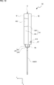
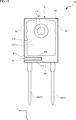
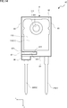
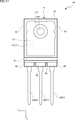
- FIG. 2 is a perspective view illustrating the semiconductor device according to the first embodiment.
- FIG. 2 is a perspective view showing the opposite side of the semiconductor device shown in FIG. 1.
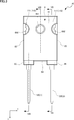
- FIG. 2 is a plan view of the semiconductor device shown in FIG. 1.
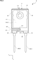
- FIG. 2 is a plan view of the semiconductor device shown in FIG. 1, which is transparent to a sealing resin.
- FIG. 2 is a bottom view of the semiconductor device shown in FIG. 1.
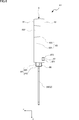
- FIG. 2 is a right side view of the semiconductor device shown in FIG. 1.
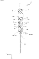
- FIG. 7 is a sectional view taken along the line VII-VII in FIG. 3.
- FIG. 8 is a cross-sectional view along the line VIII-VIII in FIG. 3. It is a bottom view showing the semiconductor device concerning a 2nd embodiment.
- FIG. 1 is a perspective view showing the opposite side of the semiconductor device shown in FIG. 1.
- FIG. 2 is a plan view of the semiconductor device shown in FIG. 1.
- FIG. 2 is a plan view of the semiconductor device shown in FIG. 1, which
- FIG. 13 is a right side view illustrating the semiconductor device according to the third embodiment. It is a bottom view showing the semiconductor device concerning a 4th embodiment. It is a right view showing the semiconductor device concerning a 5th embodiment. It is a bottom view showing the semiconductor device concerning a 6th embodiment. It is a bottom view showing the semiconductor device concerning a 7th embodiment. It is a top view showing the semiconductor device concerning an 8th embodiment, and has penetrated sealing resin. It is a bottom view showing the semiconductor device concerning an 8th embodiment. It is a bottom view showing a modification of the semiconductor device concerning an 8th embodiment. It is a top view showing the semiconductor device concerning a 9th embodiment, and has permeated sealing resin. It is a bottom view showing the semiconductor device concerning a 9th embodiment.
- FIG. 21 is a bottom view showing a modification of the semiconductor device according to the ninth embodiment. It is a bottom view showing the semiconductor device concerning a 10th embodiment.
- the semiconductor device A1 includes a plurality of leads, a semiconductor element 5, a bonding wire 71, and a sealing resin 8.
- the plurality of leads are two leads, that is, the first lead 1 and the second lead 2, but the present disclosure is not limited thereto.
- the number of leads is determined by, for example, the type of semiconductor element 5 (specifically, for example, the number of electrodes), and the number of leads can be 3 or 4, or 5 or more.
- FIG. 1 is a perspective view showing the semiconductor device A1.
- FIG. 2 is a perspective view showing the semiconductor device A1, showing the bottom side.
- FIG. 3 is a plan view showing the semiconductor device A1.
- FIG. 4 is a plan view showing the semiconductor device A1, and is transparent to the sealing resin 8 (see a two-dot chain line) for convenience of understanding.
- FIG. 5 is a bottom view showing the semiconductor device A1.
- FIG. 6 is a right side view showing the semiconductor device A1.
- FIG. 7 is a sectional view taken along the line VII-VII in FIG.
- FIG. 8 is a sectional view taken along line VIII-VIII in FIG.
- the semiconductor device A1 is, for example, a device mounted on a circuit board constituting an electronic device, but the present disclosure is not limited to this.
- three directions orthogonal to each other, that is, the x direction, the y direction, and the z direction are referred to.
- the z direction corresponds to the thickness direction of the semiconductor device A1.
- the y direction corresponds to the direction in which the terminals (120, 220) of the semiconductor device A1 extend.
- the shape of the sealing resin 8 as viewed in the z direction is substantially rectangular.
- the size of the semiconductor device A1 is not particularly limited.
- the dimension of the sealing resin 8 in the x direction is about 15 mm
- the dimension in the y direction is about 20 mm
- the dimension in the z direction is about 5 mm.
- the length of each terminal protruding from the sealing resin 8 is about 20 mm.
- the first lead 1 and the second lead 2 are electrically connected to the semiconductor element 5, and constitute a conduction path between the semiconductor element 5 and the circuit wiring when the semiconductor device A1 is mounted on the circuit board.
- the first lead 1 and the second lead 2 are formed, for example, by punching or bending a metal plate.
- the leads 1 to 3 are made of metal, preferably one of Cu and Ni, or an alloy or 42 alloy thereof. In the present embodiment, a case where the first lead 1 and the second lead 2 are made of Cu will be described as an example.
- the thickness of the first lead 1 and the second lead 2 is, for example, about 0.5 to 1 mm.
- the first lead 1 supports the semiconductor element 5 and is electrically connected to the semiconductor element 5.
- the first lead 1 includes a mounting part 110, a first terminal 120, and a connecting part 130.
- the mounting portion 110 is a portion on which the semiconductor element 5 is mounted, and has a substantially rectangular shape as viewed in the z direction.
- the mounting section 110 has a mounting section main surface 111 and a mounting section back surface 112.
- the mounting portion main surface 111 and the mounting portion back surface 112 face opposite sides in the z direction.
- the mounting portion main surface 111 is a surface facing the left side in FIGS.
- the mounting portion main surface 111 is a surface on which the semiconductor element 5 is mounted.
- the mounting portion rear surface 112 is a surface facing the right side in FIGS.
- the mounting portion rear surface 112 is exposed from the sealing resin 8 and becomes a rear surface terminal.
- the mounting portion 110 has a mounting portion through hole 113 penetrating in parallel from the mounting portion main surface 111 to the mounting portion back surface 112 in the z direction.
- the mounting portion through hole 113 is disposed at the center of the mounting portion 110 in the x direction and near one end in the y direction (upward in FIG. 4), and has a circular shape as viewed in the z direction.
- the position and shape of the mounting portion through-hole 113 are not limited to the illustrated example.
- the first terminal 120 extends in the y-direction, and a part thereof is exposed from the sealing resin 8.
- the first terminal 120 is electrically connected to the semiconductor element 5 via the connecting part 130 and the mounting part 110.
- the connecting part 130 is connected to the mounting part 110 and the first terminal 120, and connects the mounting part 110 and the first terminal 120. As shown in FIG. 8, the mounting section 110 and the first terminal 120 are different in the position in the z direction, and the first terminal 120 is located on the left side in FIG. Therefore, the connecting part 130 is inclined with respect to the mounting part 110 and the first terminal 120. If the position in the z direction is the same between the mounting portion main surface 111 and the surface of the first terminal 120 on the same side as the mounting portion main surface 111, the connecting portion 130 does not need to be inclined.
- the connecting portion 130 is entirely covered with the sealing resin 8.
- the thickness (dimension in the z direction) of the first terminal 120 and the connecting portion 130 is the same, and is smaller than the thickness of the mounting portion 110.
- the first terminal 120 and the connecting portion 130 are formed by, for example, a half etching process.
- the thickness of the mounting part 110 may be the same as the thickness of the first terminal 120 and the connecting part 130.
- the connecting portion 130 and the first terminal 120 are arranged below the mounting portion 110 in the y direction and to the left in the x direction.
- a virtual line C ⁇ b> 1 (dashed line) obtained by extending the center line of the first terminal 120 in the y direction does not intersect with the semiconductor element 5 and the mounting portion through hole 113.
- the position of the first terminal 120 in the x direction is not limited to the illustrated example.
- the second lead 2 is electrically connected to the semiconductor element 5.
- the second lead 2 is disposed apart from the first lead 1, and as shown in FIG. 4, is disposed below the mounting portion 110 of the first lead 1 in the y direction and to the right in the x direction.
- the second lead 2 includes a wire bonding unit 210 and a second terminal 220.
- the wire bonding portion 210 is a portion to which the bonding wire 71 is bonded, and has a rectangular shape long in the x direction when viewed in the z direction. As shown in FIG. 7, the wire bonding unit 210 has a wire bonding unit main surface 211 and a wire bonding unit back surface 212. The wire bonding portion main surface 211 and the wire bonding portion back surface 212 face opposite sides in the z direction.
- the wire bonding portion main surface 211 is a surface facing the left side in FIGS.
- the wire bonding portion main surface 211 is a surface to which the bonding wire 71 is bonded (see FIG. 4).
- the wire bonding portion back surface 212 is a surface facing the right side in FIGS.
- the wire bonding section 210 is entirely covered with the sealing resin 8.
- the second terminal 220 is connected to the wire bonding portion 210, extends in the y direction, and partially exposes from the sealing resin 8.
- the second terminal 220 is electrically connected to the semiconductor element 5 via the wire bonding part 210 and the bonding wire 71.
- the thickness (dimension in the z direction) of the wire bonding portion 210 and the second terminal 220 is the same, and is the same as the thickness of the first terminal 120 and the connecting portion 130 of the first lead 1.
- the portion of the first terminal 120 exposed from the sealing resin 8 and the portion of the second terminal 220 exposed from the sealing resin 8 have the same shape, and have the tip of the first terminal 120 (connected to the connecting portion 130).
- the end of the second terminal 220 (the end opposite to the portion connected to the wire bonding portion 210) and the tip of the second terminal 220 (the end opposite to the portion connected to the wire bonding portion 210) are at the same position in the y direction. As shown in FIG.
- a virtual line C ⁇ b> 2 (dashed line) obtained by extending the center line of the second terminal 220 in the y direction does not intersect with the semiconductor element 5 and the mounting portion through hole 113.
- the position of the second terminal 220 in the x direction is not limited to the illustrated example. It is desirable that the first terminal 120 and the second terminal 220 are separated in the x direction.
- the semiconductor element 5 is an element that exhibits the electrical function of the semiconductor device A1.
- the semiconductor element 5 is a diode.
- the semiconductor element 5 includes an element main body 50, an element main surface 51, an element back surface 52, a first electrode 53, and a second electrode 54.
- the element main surface 51 and the element back surface 52 face opposite sides in the z direction.
- the element main surface 51 is a surface facing the left side in FIGS.
- the element back surface 52 is a surface facing the right side in FIGS.
- the first electrode 53 is arranged on the back surface 52 of the element.
- the second electrode 54 is arranged on the element main surface 51.
- the first electrode 53 is a cathode electrode
- the second electrode 54 is an anode electrode.
- the semiconductor element 5 is mounted at the center of the mounting portion main surface 111 in the x direction and at a position that does not cover the mounting portion through hole 113 when viewed in the z direction.
- the semiconductor element 5 is mounted on the mounting portion main surface 111 via the conductive bonding material 59 with the element back surface 52 facing the mounting portion main surface 111.
- the first electrode 53 of the semiconductor element 5 is joined to the mounting portion main surface 111 by the joining material 59 and is electrically connected to the first lead 1.
- the bonding material 59 include a TiNiAg-based solder, a SnAgCu-based solder, and a conductive bonding material formed using baked Ag. As shown in FIG.
- the bonding wire 71 is connected to the second electrode 54 of the semiconductor element 5 and the wire bonding portion 210 of the second lead 2. Thereby, the second electrode 54 of the semiconductor element 5 is electrically connected to the second lead 2.
- the material of the bonding wire 71 is not particularly limited. In the present embodiment, a wire made of, for example, Al is used. Further, the number of bonding wires 71 is not limited.
- the first terminal 120 of the first lead 1 conducting to the first electrode 53 functions as the cathode terminal of the semiconductor device A1
- the second terminal 220 of the second lead 2 conducting to the second electrode 54 is the anode terminal of the semiconductor device A1. Function as
- the sealing resin 8 covers a part of each of the first lead 1 and the second lead 2, the semiconductor element 5, and the bonding wire 71.
- the sealing resin 8 is made of, for example, a black epoxy resin.
- the sealing resin 8 has a resin main surface 81, a resin back surface 82, a resin side surface 83, and a resin end surface 84.
- the resin main surface 81 and the resin back surface 82 face opposite sides in the z direction.
- the resin main surface 81 is a surface facing the left side in FIGS. 6 to 8
- the resin back surface 82 is a surface facing the right side in FIGS.
- the mounting portion back surface 112 of the first lead 1 is entirely exposed from the resin back surface 82, and the resin back surface 82 and the mounting portion back surface 112 face each other. Are one.
- the resin side surface 83 is a surface connecting the resin main surface 81 and the resin back surface 82, and is a pair of surfaces facing the x direction.
- the pair of resin side surfaces 83 face opposite sides.
- Each resin side surface 83 includes a first side surface 831 and a second side surface 832. As shown in FIGS. 1 and 2, each first side surface 831 is connected to the resin main surface 81, and is inclined so as to approach each other toward the resin main surface 81.
- Each second side surface 832 is connected to the resin back surface 82, and is inclined so as to approach each other toward the resin back surface 82. In the present embodiment, the boundary between the first side surface 831 and the second side surface 832 is closer to the resin back surface 82.
- the resin end surface 84 is a surface that connects the resin main surface 81 and the resin back surface 82, and is a surface that faces the direction in which the first terminal 120 and the second terminal 220 protrude (a surface that faces downward in the y direction in FIG. 3). .
- the resin end faces 84 are respectively connected to the pair of resin side faces 83.
- the resin end surface 84 includes a first end surface 841 and a second end surface 842. As shown in FIGS. 1, 2, and 6, the first end surface 841 of the resin end surface 84 is connected to the resin main surface 81, and is inclined so as to approach the center of the sealing resin 8 toward the resin main surface 81. doing.
- the second end surface 842 is connected to the resin back surface 82, and is inclined so as to approach the center of the sealing resin 8 toward the resin back surface 82.
- a portion of the sealing resin 8 surrounded by the pair of first side surfaces 831 and the first end surfaces 841 has a tapered shape in which the cross-sectional area on the xy plane decreases toward the resin main surface 81
- the portion surrounded by the second side surface 832 and the second end surface 842 has a tapered shape in which the cross-sectional area in the xy plane decreases toward the resin back surface 82.
- the sealing resin 8 includes a resin through hole 891, a side recess 892, end protrusions 85 and 86, and a back groove 87.
- the resin through hole 891 is a through hole penetrating from the resin main surface 81 to the resin back surface 82 in parallel in the z direction.
- the resin through hole 891 is disposed at the center in the x direction of the sealing resin 8 and near one end in the y direction (upward in FIG. 3), and has a circular shape as viewed in the z direction.
- the center of the resin through hole 891 is the same as the center of the mounting portion through hole 113.
- the diameter of the resin through hole 891 is smaller than the diameter of the mounting portion through hole 113. Therefore, as shown in FIGS. 2 and 5, the resin through hole 891 is located inside the mounting portion through hole 113, and the entire wall of the resin through hole 891 is formed by the sealing resin 8.
- the mounting portion 110 is not exposed from the hole wall of the resin through hole 891.
- the resin through hole 891 is used for inserting a fastening member such as a screw and attaching a heat radiating member to the semiconductor device A1.
- a fastening member such as a screw
- a heat radiating member to the semiconductor device A1.
- the side recess 892 is a recess recessed from the first side surface 831 of the resin side surface 83 and the resin main surface 81, and is formed on each of the first side surfaces 831.
- each side recess 892 has a semicircular shape as viewed in the z direction, and is formed so as to sandwich the resin through hole 891.
- a part of the mounting portion main surface 111 of the first lead 1 is exposed from the sealing resin 8 by a side recess 892.
- each side recess 892 has a shape such that the cross-sectional area on the xy plane increases toward the resin main surface 81.
- the shape and arrangement position of the side recess 892 are not limited to the illustrated example.
- the end face convex portions 85 and 86 are portions projecting from the resin end face 84 in the y direction, and have a substantially rectangular parallelepiped shape.
- the shape of the end face convex portions 85 and 86 is not particularly limited, and may be, for example, a columnar shape.
- the end face protrusion 85 and the end face protrusion 86 are arranged apart from each other in the x direction.
- the first terminal 120 of the first lead 1 protrudes from the end surface protrusion 85, and the second terminal 220 of the second lead 2 protrudes from the end surface protrusion 86.
- the end surface protrusion 86 is an example of the “end surface protrusion” of the present disclosure
- the end surface protrusion 85 is an example of the “second end surface protrusion” of the present disclosure.
- the back surface groove 87 is a groove formed so as to be recessed from the resin back surface 82 and extending along the x direction, and has a square cross section in the yz plane.
- the cross section parallel to the first side surface 831 or the second side surface 832 is also rectangular.
- the back surface groove portion 87 includes a groove bottom surface 871 and a pair of groove side surfaces 872.
- the groove bottom surface 871 is a surface parallel to the resin back surface 82 and is located closer to the resin main surface 81 than the resin back surface 82.
- the pair of groove side surfaces 872 are connected to the groove bottom surface 871 and the resin back surface 82, respectively, and are surfaces facing each other.
- the back surface groove 87 is shaped such that the cross-sectional area in the xy plane increases toward the resin back surface 82.
- Each of the pair of groove side surfaces 872 is inclined by about 3 to 5 ° with respect to the xz plane.
- the inclination degree of the groove side surface 872 is not limited to the illustrated example, and may not be inclined.
- the depth (dimension in the z direction) of the back surface groove 87 is, for example, about 1 mm, and the width (dimension in the y direction) of the back surface groove 87 is, for example, about 1 mm.
- the back surface groove portion 87 is disposed between one end (the lower end in FIG. 5) of the resin back surface 82 in the y direction and the mounting portion back surface 112 when viewed in the z direction.
- One end of the back surface groove portion 87 extends to the resin side surface 83 on the second terminal 220 side, and is open to the resin side surface 83.
- the other end of the back surface groove 87 extends to near the center of the resin back surface 82 in the x direction.
- the back surface groove portion 87 is elongated along the x direction, but ends before the first lead 1.
- the back surface groove portion 87 is disposed between the boundary between the second terminal 220 and the resin end surface 84 and the mounting portion back surface 112.
- the back surface groove portion 87 does not overlap the first lead 1 when viewed in the z direction.
- the back surface groove portion 87 has a groove bottom surface 871 whose position in the z direction is separated from the resin back surface 82 toward the resin main surface 81 side.
- the back surface groove portion 87 is an example of the “back surface displacement portion” of the present disclosure.
- the sealing resin 8 includes the back surface groove 87 recessed from the resin back surface 82.
- the creepage distance (the distance measured along the surface of the sealing resin 8) between the exposed portion of the second terminal 220 from the sealing resin 8 and the back surface 112 of the mounting portion is smaller than the case where the back surface groove 87 is not provided. Can also be longer. The longer the creepage distance, the higher the withstand voltage between the second terminal 220 and the mounting portion rear surface 112 can be increased. Therefore, the semiconductor device A1 can achieve high withstand voltage.
- the sealing resin 8 includes the end surface protrusion 86 protruding from the resin end surface 84, and the second terminal 220 protrudes from the end surface protrusion 86.
- the creepage distance between the exposed portion of the second terminal 220 from the sealing resin 8 and the back surface 112 of the mounting portion can be extended by the dimension of the end surface convex portion 86 in the y direction. Therefore, the withstand voltage between the second terminal 220 and the mounting portion rear surface 112 can be further increased.
- the end surface convex portion 86 can also increase the creeping distance between the first terminal 120 and the second terminal 220. Thereby, the withstand voltage between the first terminal 120 and the second terminal 220 can be increased.
- the sealing resin 8 includes the end surface protrusion 85 protruding from the resin end surface 84, and the first terminal 120 protrudes from the end surface protrusion 85.
- the creeping distance between the first terminal 120 and the second terminal 220 can be further extended by the dimension of the end face protrusion 85 in the y direction. Therefore, the withstand voltage between the first terminal 120 and the second terminal 220 can be further increased.
- FIG. 9 is a bottom view showing the semiconductor device A2, and corresponds to FIG. 5 of the semiconductor device A1 according to the first embodiment.
- the semiconductor device A2 is different from the semiconductor device A1 in the shape of the back surface groove 87.
- the dimension of the back surface groove 87 in the x direction is small.
- One end of the back surface groove 87 does not extend to the resin side surface 83 on the second terminal 220 side, and the back surface groove 87 does not open to the resin side surface 83.
- the other end of the back surface groove 87 does not extend to the vicinity of the center of the resin back surface 82 in the x direction, and extends only to a position closer to the resin side surface 83 on the second terminal 220 side as compared with the first embodiment.
- the back surface groove portion 87 is formed when the creeping distance from the second terminal 220 to the mounting portion back surface 112 bypassing the back surface groove portion 87 (shown by a broken line in FIG. 9) crosses the back surface groove portion 87 (shown by a dashed line in FIG. 9). ) Is formed to be longer than the creepage distance.
- the creepage distance between the exposed portion of the second terminal 220 from the sealing resin 8 and the mounting portion rear surface 112 can be extended. Therefore, also in the present embodiment, the same effects as in the first embodiment can be obtained.
- the creepage distance from the second terminal 220 to the mounting portion back surface 112 bypassing the back surface groove 87 is shorter than the creepage distance when crossing the back surface groove 87, the case where the back surface groove 87 is not formed is the same as the case where the back surface groove 87 is not formed.
- the creepage distance between the exposed portion of the second terminal 220 from the sealing resin 8 and the back surface 112 of the mounting portion can be extended. Therefore, even in such a case, the back surface groove portion 87 contributes to a higher withstand voltage of the semiconductor device A2.
- FIG. 10 is a right side view illustrating the semiconductor device A3, and corresponds to FIG. 6 of the semiconductor device A1 according to the first embodiment.
- the semiconductor device A3 is different from the semiconductor device A1 in the shape of the back surface groove 87.
- the cross section of the back surface groove 87 in the yz plane is triangular.
- the creepage distance between the exposed portion of the second terminal 220 from the sealing resin 8 and the mounting portion rear surface 112 can be extended. Therefore, also in the present embodiment, the same effects as in the first embodiment can be obtained.
- the cross-sectional shape of the back surface groove 87 in the yz plane is not limited to the illustrated example, and may be another shape. For example, the shape may be semicircular.
- FIG. 11 is a bottom view showing the semiconductor device A4, and corresponds to FIG. 5 of the semiconductor device A1 according to the first embodiment.
- the semiconductor device A4 differs from the semiconductor device A1 in that it has two back surface grooves 87.
- the sealing resin 8 includes two back surface groove portions 87 arranged so as to be arranged in the y direction. According to the present embodiment, the creepage distance between the exposed portion of the second terminal 220 from the sealing resin 8 and the back surface 112 of the mounting portion can be further extended as compared with the case where only one back surface groove 87 is provided. Therefore, also in the present embodiment, the same effects as in the first embodiment can be obtained.
- the number of the back surface groove portions 87 is not limited, and may be three or more.
- FIG. 12 is a right side view illustrating the semiconductor device A5, and corresponds to FIG. 6 of the semiconductor device A1 according to the first embodiment.
- the semiconductor device A5 is different from the semiconductor device A1 in that the semiconductor device A5 includes a rear surface convex portion 88 instead of the rear surface groove portion 87.
- the back surface convex portion 88 is formed so as to protrude from the resin back surface 82 and has a shape extending long in the x direction.
- the back surface projection 88 has a square cross section in the yz plane.
- the cross-sectional shape of the back surface protruding portion 88 parallel to the first side surface 831 or the second side surface 832 is a quadrangle.
- the rear surface convex portion 88 includes a convex main surface 881 and a pair of convex side surfaces 882.
- the convex main surface 881 is a surface parallel to the resin back surface 82, and is located on the opposite side of the resin main surface 81 with respect to the resin back surface 82.
- the pair of convex side surfaces 882 are connected to the convex main surface 881 and the resin back surface 82, respectively, and are surfaces facing each other.
- the rear surface convex portion 88 has a tapered shape in which the cross-sectional area in the xy plane decreases as the distance from the resin rear surface 82 increases.
- Each of the pair of convex side surfaces 882 is inclined by about 3 to 5 ° with respect to the xz plane.
- the degree of inclination of the convex side surface 882 is not limited to the illustrated example, and may not be inclined.
- the height (dimension in the z direction) of the back surface protrusion 88 is, for example, about 1 mm, and the width (for example, the average value, the maximum value, or the minimum value of the size in the y direction) of the back surface protrusion 88 is, for example, about 1 mm. is there.
- the size of the rear surface projection 88 in the x direction and the arrangement position in the z direction are the same as those of the rear surface groove 87 of the first embodiment. That is, the rear surface protrusion 88 is disposed between one end of the resin rear surface 82 in the y direction and the mounting portion rear surface 112 when viewed in the z direction. One end of the back surface protruding portion 88 extends to the resin side surface 83 on the second terminal 220 side, and the other end extends to near the center of the resin back surface 82 in the x direction. That is, the back surface protruding portion 88 is disposed between the boundary between the second terminal 220 and the resin end surface 84 and the mounting portion back surface 112.
- the rear surface projection 88 does not overlap the first lead 1 when viewed in the z direction.
- the rear surface convex portion 88 has a convex main surface 881 whose position in the z direction is separated from the resin rear surface 82 on the side opposite to the resin main surface 81.
- the back surface convex portion 88 is an example of the “back surface displacement portion” of the present disclosure.
- the sealing resin 8 has the back surface convex portion 88 formed so as to protrude from the resin back surface 82. Therefore, the creepage distance between the exposed portion of the second terminal 220 from the sealing resin 8 and the mounting portion rear surface 112 can be extended. Therefore, also in the present embodiment, the same effects as in the first embodiment can be obtained.
- the cross-sectional shape of the rear surface projection 88 on the yz plane is not limited, and may be another shape. For example, it may be triangular or semicircular.
- the sealing resin 8 may include a plurality of back surface protrusions 88 arranged so as to be arranged in the y direction.
- FIG. 13 is a bottom view showing the semiconductor device A6, and corresponds to FIG. 5 of the semiconductor device A1.
- the semiconductor device A6 is different from the semiconductor device A1 in that the semiconductor device A6 does not include the end surface protrusions 85 and 86.
- the first terminal 120 and the second terminal 220 protrude from the resin end surface 84.
- the sealing resin 8 since the sealing resin 8 includes the back surface groove 87, the creepage distance between the exposed portion of the second terminal 220 from the sealing resin 8 and the mounting portion back surface 112 can be extended. Accordingly, the withstand voltage of the semiconductor device A6 can also be increased.
- FIG. 14 is a bottom view showing the semiconductor device A7, and corresponds to FIG. 5 of the semiconductor device A1.
- the semiconductor device A7 is different from the semiconductor device A1 in that the semiconductor device A7 does not include the end surface protrusion 85.
- the first terminal 120 protrudes from the resin end surface 84.
- the sealing resin 8 since the sealing resin 8 includes the back surface groove 87, the creepage distance between the exposed portion of the second terminal 220 from the sealing resin 8 and the mounting portion back surface 112 can be extended. Accordingly, the withstand voltage of the semiconductor device A6 can also be increased. Also in the present embodiment, since the sealing resin 8 has the end surface convex portion 86, the creepage distance between the exposed portion of the second terminal 220 from the sealing resin 8 and the mounting portion back surface 112 can be extended. Can be. Therefore, the withstand voltage between the second terminal 220 and the mounting portion rear surface 112 can be further increased. The end surface protrusion 86 can also increase the creeping distance between the first terminal 120 and the second terminal 220. Thereby, the withstand voltage between the first terminal 120 and the second terminal 220 can be increased.
- FIG. 15 is a plan view of relevant parts showing the semiconductor device A8, and corresponds to FIG. 4 of the semiconductor device A1 according to the first embodiment.
- FIG. 16 is a bottom view showing the semiconductor device A8, and corresponds to FIG. 5 of the semiconductor device A1.
- the semiconductor device A8 differs from the semiconductor device A1 in that the semiconductor device A8 includes a semiconductor element 6 instead of the semiconductor element 5.
- the semiconductor device A8 has three terminals according to the number of electrodes of the semiconductor element 6.
- the semiconductor device A8 includes a first lead 1, a second lead 2, a third lead 3, a semiconductor element 6, bonding wires 71 and 72, and a sealing resin 8.
- the first lead 1 and the second lead 2 are similar to the first lead 1 and the second lead 2 according to the first embodiment, and are electrically connected to the semiconductor element 6, and the semiconductor device A8 is mounted on a circuit board. Sometimes, a conduction path between the semiconductor element 6 and the circuit wiring is formed.
- the connecting portion 130 and the first terminal 120 of the first lead 1 according to the present embodiment are arranged below the mounting portion 110 in the y direction and at the center in the x direction.
- an imaginary line C ⁇ b> 1 (dashed line) obtained by extending the center line of the first terminal 120 in the y direction intersects the semiconductor element 5 and the mounting portion through-hole 113. Further, as shown in FIG.
- the second lead 2 is disposed below the mounting portion 110 of the first lead 1 in the y direction and to the right in the x direction.
- An imaginary line C2 (dashed line) obtained by extending the center line of the second terminal 220 in the y direction does not intersect with the semiconductor element 5 and the mounting portion through-hole 113.
- the third lead 3 is also electrically connected to the semiconductor element 6, and forms a conduction path between the semiconductor element 6 and the circuit wiring when the semiconductor device A8 is mounted on the circuit board. I do.
- the material, dimensions and shape of the third lead 3 are the same as those of the second lead 2.
- the third lead 3 is disposed apart from the first lead 1 and the second lead 2, and is disposed below the mounting portion 110 of the first lead 1 in the y direction and to the left in the x direction, as shown in FIG. ing.
- the third lead 3 includes a wire bonding section 310 and a third terminal 320.
- the wire bonding portion 310 is a portion to which the bonding wire 72 is bonded, and has a rectangular shape long in the x direction when viewed in the z direction.
- the wire bonding portion 310 has a wire bonding portion main surface 311 and a wire bonding portion back surface 312.
- the wire bonding portion main surface 311 and the wire bonding portion back surface 312 face opposite sides in the z direction.
- the wire bonding portion main surface 311 is a surface facing the near side in FIG.
- the wire bonding portion main surface 311 is a surface to which the bonding wire 72 is bonded.
- the wire bonding portion back surface 312 is a surface facing the back side in FIG.
- the wire bonding portion 310 is entirely covered with the sealing resin 8.
- the third terminal 320 is connected to the wire bonding portion 310, extends in the y direction, and partially exposes from the sealing resin 8.
- the third terminal 320 is electrically connected to the semiconductor element 5 via the wire bonding portion 310 and the bonding wire 72.
- the thickness (dimension in the z direction) of the wire bonding portion 310 and the third terminal 320 is the same, and is the same as the wire bonding portion 210 and the second terminal 220 of the second lead 2.
- the part of the third terminal 320 exposed from the sealing resin 8 has the same shape as the part of the first terminal 120 and the second terminal 220 exposed from the sealing resin 8.
- the tip of the third terminal 320 (the end opposite to the portion connected to the wire bonding portion 310) is located at the same position as the tip of the first terminal 120 and the second terminal 220 in the y direction.
- a virtual line C ⁇ b> 3 (dashed line) obtained by extending the center line of the third terminal 320 in the y direction does not intersect with the semiconductor element 5 and the mounting portion through hole 113.
- the semiconductor element 6 is an element that exhibits the electrical function of the semiconductor device A8.
- the semiconductor element 6 is a transistor such as a MOSFET (metal-oxide-semiconductor field-effect transistor).
- the semiconductor element 6 includes an element body 60, an element main surface 61, an element back surface (corresponding to the element back surface 52 in FIG. 8), a first electrode (corresponding to the first electrode 53 in FIG. 8), a second electrode 64, and a third electrode. 65.
- the element main surface 61 and the element back surface face each other in the z direction.
- the element main surface 61 is a surface facing the near side in FIG.
- the back surface of the element is a surface facing the back side in FIG.
- the first electrode is arranged on the back surface of the device.
- the second electrode 64 and the third electrode 65 are arranged on the element main surface 61.
- the first electrode is a drain electrode
- the second electrode 64 is a source electrode
- the third electrode 65 is a gate electrode.
- the semiconductor element 6 is mounted at the center of the mounting portion main surface 111 in the x direction and at a position that does not cover the mounting portion through hole 113 when viewed in the z direction.
- the semiconductor element 6 is mounted on the mounting portion main surface 111 via the conductive bonding material 59 with the element back surface facing the mounting portion main surface 111.
- the first electrode of the semiconductor element 6 is joined to the mounting portion main surface 111 by the joining material 59 and is electrically connected to the first lead 1.
- the bonding wire 71 is connected to the second electrode 64 of the semiconductor element 6 and the wire bonding portion main surface 211 of the second lead 2.
- the second electrode 64 of the semiconductor element 6 is electrically connected to the second lead 2.
- the bonding wire 72 is connected to the third electrode 65 of the semiconductor element 6 and the wire bonding portion main surface 311 of the third lead 3.
- the third electrode 65 of the semiconductor element 6 is electrically connected to the third lead 3.
- the material, thickness and number of the bonding wires 71 and 72 are not limited.
- the first terminal 120 of the first lead 1 conducting to the first electrode 1 functions as a drain terminal of the semiconductor device A8, and the second terminal 220 of the second lead 2 conducting to the second electrode 64 serves as a source terminal of the semiconductor device A8.
- the third terminal 320 of the third lead 3 that functions and conducts to the third electrode 65 functions as the gate terminal of the semiconductor device A8.
- the sealing resin 8 according to the present embodiment is the same as the sealing resin 8 according to the first embodiment, and further includes an end surface convex portion 86 ′ and a back surface groove portion 87 ′.
- the end surface convex portion 86 ’ is a portion that protrudes in the y direction from the resin end surface 84, like the end surface convex portions 85, 86, and has a substantially rectangular parallelepiped shape.
- the end surface convex portion 85 is arranged at the center in the x direction according to the arrangement of the first terminal 120, the second terminal 220, and the third terminal 320, and the end surface convex portion 86 is
- the end face protrusion 86 ′ is arranged away from the protrusion 85 and to the left in the x direction, and the end face protrusion 86 ′ is arranged away from the end face to the right in the x direction.
- the third terminal 320 of the third lead 3 protrudes from the end surface convex portion 86 '.
- the “back surface groove portion 87” is a groove formed in the resin back surface 82 and extending in the x direction, similarly to the back surface groove portion 87.
- the shape and configuration of the back surface groove 87 ′ are the same as those of the back surface groove 87.
- the back surface groove portion 87 ′ is arranged between one end (the lower end in FIG. 16) of the resin back surface 82 in the y direction and the mounting portion back surface 112 when viewed in the z direction.
- One end of the back surface groove portion 87 ′ extends to the resin side surface 83 on the third terminal 320 side, and is open to the resin side surface 83.
- the other end of the back surface groove 87 ′ extends to a position just before the center in the x direction of the resin back surface 82.
- the other end of the back surface groove portion 87 also extends to a position just before the center in the x direction of the resin back surface 82. That is, the back surface groove portion 87 ′ is disposed between the boundary between the third terminal 320 and the resin end surface 84 and the mounting portion back surface 112. Further, the back surface groove portion 87 'does not overlap with the first lead 1 as viewed in the z direction.
- the back surface groove portion 87 ' has a groove bottom surface whose position in the z direction has moved away from the resin back surface 82 toward the resin main surface 81, and is an example of the "second back surface displacement portion" of the present disclosure.
- the sealing resin 8 further includes a back surface groove 87 ′ formed so as to be recessed from the resin back surface 82.
- the creepage distance between the exposed portion of the third terminal 320 from the sealing resin 8 and the mounting portion rear surface 112 can be extended. Therefore, the withstand voltage between the third terminal 320 and the mounting portion rear surface 112 can be increased.
- the sealing resin 8 further includes an end surface protrusion 86 ′ protruding from the resin end surface 84, and the third terminal 320 protrudes from the end surface protrusion 86 ′.
- the creepage distance between the exposed portion of the third terminal 320 from the sealing resin 8 and the mounting portion rear surface 112 can be extended by the dimension of the end surface convex portion 86 in the y direction. Therefore, the withstand voltage between the third terminal 320 and the mounting portion rear surface 112 can be further increased.
- the end surface convex portion 86 ′ can also increase the creeping distance between the first terminal 120 and the third terminal 320. Thereby, the withstand voltage between the first terminal 120 and the third terminal 320 can be increased.
- the other end of the back surface groove 87 may be extended to extend to the resin side surface 83 on the third terminal 320 side.
- FIG. 18 is a plan view of relevant parts showing the semiconductor device A9, and corresponds to FIG. 4 of the semiconductor device A1 according to the first embodiment.
- FIG. 19 is a bottom view showing the semiconductor device A9, and corresponds to FIG. 5 of the semiconductor device A1 according to the first embodiment.
- the semiconductor device A9 according to the present embodiment is different from the semiconductor device A8 according to the eighth embodiment in the arrangement of the first terminal 120 and the third terminal 320.
- connection portion 130 and the first terminal 120 of the first lead 1 and the arrangement of the second lead 2 according to the present embodiment are the same as those of the semiconductor device A1 according to the first embodiment. That is, the connecting portion 130 and the first terminal 120 of the first lead 1 are arranged below the mounting portion 110 in the y direction and to the left in the x direction, as shown in FIG. An imaginary line C ⁇ b> 1 (dashed line) obtained by extending the center line of the first terminal 120 in the y direction does not intersect with the semiconductor element 5 and the mounting portion through hole 113. Further, as shown in FIG. 18, the second lead 2 is disposed below the mounting portion 110 of the first lead 1 in the y direction and to the right in the x direction.
- An imaginary line C2 (dashed line) obtained by extending the center line of the second terminal 220 in the y direction does not intersect with the semiconductor element 5 and the mounting portion through-hole 113.
- the third lead 3 according to the present embodiment is disposed apart from the first lead 1 and the second lead 2, and as shown in FIG. It is arranged at the center in the direction.
- the sealing resin 8 according to the present embodiment is different from the eighth embodiment in that the shape of the end face protrusion 86 is not provided with the end face protrusion 86 ′. Further, the arrangement of the end surface convex portions 85 and 86 is also different from the case of the eighth embodiment. As shown in FIG. 19, in the present embodiment, the end surface protrusion 85 is arranged on the right side in the x direction in accordance with the arrangement of the first terminal 120, the second terminal 220, and the third terminal 320, and the end surface protrusion 86 is formed on the end surface. It is arranged on the left side in the x direction away from the protrusion 85.
- the end face protrusion 86 has a larger dimension in the x direction than in the eighth embodiment, and extends from the left end in the x direction to near the end face protrusion 85.
- the second terminal 220 of the second lead 2 and the third terminal 320 of the third lead 3 protrude from the end surface convex portion 86.
- the sealing resin 8 according to the present embodiment does not include the back surface groove 87 ′.
- the dimension of the back surface groove 87 in the x direction is larger than that in the eighth embodiment, and the other end of the back surface groove 87 extends between the end face protrusion 85 and the end face protrusion 86. That is, the back surface groove 87 extends between the boundary between the third terminal 320 and the resin end surface 84 and the mounting portion back surface 112. Further, the back surface groove portion 87 does not overlap with the first lead 1 as viewed in the z direction.
- the same effects as in the first embodiment can be obtained.
- the back surface groove 87 extends to between the end surface convex portion 85 and the end surface convex portion 86. Therefore, the creepage distance between the exposed portion of the third terminal 320 from the sealing resin 8 and the mounting portion rear surface 112 can be extended. Therefore, the withstand voltage between the third terminal 320 and the mounting portion rear surface 112 can be increased.
- the third terminal 320 protrudes from the end surface convex portion 86.
- the creepage distance between the exposed portion of the third terminal 320 from the sealing resin 8 and the mounting portion rear surface 112 can be extended by the dimension of the end surface convex portion 86 in the y direction. Therefore, the withstand voltage between the third terminal 320 and the mounting portion rear surface 112 can be further increased.
- the end surface protrusion 86 can also increase the creeping distance between the first terminal 120 and the third terminal 320. Thereby, the withstand voltage between the first terminal 120 and the third terminal 320 can be increased.
- the back surface groove portion 87 is not extended, but the back surface groove portion 87 is disposed between the boundary between the second terminal 220 and the resin end surface 84 and the mounting portion back surface 112.
- the groove 87 ′ may be arranged between the boundary between the third terminal 320 and the resin end surface 84 and the mounting portion rear surface 112.
- the back surface groove portion 87 ′ has a groove bottom surface whose position in the z direction is separated from the resin back surface 82 toward the resin main surface 81.
- the back surface groove portion 87 ' is an example of the "second back surface displacement portion" of the present disclosure.
- FIG. 21 is a bottom view showing the semiconductor device A10, and corresponds to FIG. 5 of the semiconductor device A1 according to the first embodiment.
- the semiconductor device A10 of the present embodiment is different from the semiconductor device A9 of the ninth embodiment in the following points. That is, the semiconductor device A10 includes the semiconductor element 7 having four electrodes. In addition, the semiconductor device A10 includes four leads that are electrically connected to the four electrodes. Specifically, the semiconductor element 7 includes a drain electrode D, a gate electrode G, a driver source electrode DS, and a power source electrode PS. As shown in FIG. 21, the drain electrode D conducts to the lead 1. Similarly, the gate electrode G is electrically connected to the lead 2, the driver source electrode DS is electrically connected to the lead 3, and the power source electrode PS is electrically connected to the lead 4. The leads 1 to 3 have terminals 120, 220, and 320, respectively.
- the lead 4 has a terminal 420.
- the terminals 220, 320, and 420 are equally spaced from each other in the x direction.
- the distance between the terminal 120 (drain terminal) and the terminal 420 (power source terminal) is larger than the distance between the terminal 320 (driver source terminal) and the terminal 420 (power source terminal).
- the present disclosure is not limited to this.
- the sealing resin 8 has the back surface groove 87 extending in the x direction.
- the back surface groove portion 87 continuously extends from the left edge portion of the sealing resin 8 and terminates before the drain terminal 120 (between the end surface convex portion 85 and the end surface convex portion 86). I have.
- the present disclosure is not limited to this example.
- the back surface groove 87 may extend from the left edge to the right edge of the sealing resin 8, or as shown in FIG. 87, 87 ′).
- an additional back surface groove may be formed in the sealing resin 8.
- a back surface protrusion (see reference numeral 88 in FIG. 12) that protrudes from the resin back surface 82 in the z direction may be provided.
- a back surface protrusion (see reference numeral 88 in FIG. 12) that protrudes from the resin back surface 82 in the z direction may be provided.
- the semiconductor device according to the present disclosure is not limited to the embodiments described above.
- the specific configuration of each part of the semiconductor device according to the present disclosure can be variously changed in design.
- Appendix 1 A semiconductor element having an element main surface and an element back surface facing each other in the thickness direction, a first electrode disposed on the element back surface, and a second electrode disposed on the element main surface; A mounting portion main surface to which the first electrode of the semiconductor element is bonded, and a mounting portion having a mounting portion rear surface facing the opposite side to the mounting portion main surface in the thickness direction, and via the mounting portion.
- a first lead having a first terminal electrically connected to the first electrode;
- a second lead having a second terminal electrically connected to the second electrode;
- a sealing resin that covers a part of each of the first lead and the second lead and the semiconductor element; The first terminal and the second terminal protrude from the sealing resin,
- the sealing resin connects the resin main surface and the resin back surface facing the opposite sides in the thickness direction with the resin main surface and the resin back surface, and has a direction in which the first terminal and the second terminal protrude.
- the sealing resin has a rear surface displacement having a portion separated from the resin rear surface in the thickness direction between a boundary between the second terminal and the resin end surface and the mounting portion rear surface on the resin rear surface side.
- a semiconductor device comprising a unit. Appendix 2 The semiconductor device according to claim 1, wherein the rear surface displacement portion does not overlap with the first lead when viewed in the thickness direction. Appendix 3 The semiconductor device according to claim 1 or 2, wherein the rear surface displacement portion extends to the resin side surface on the second terminal side.
- Appendix 4 The semiconductor device according to any one of supplementary notes 1 to 3, wherein the rear surface displacement portion has a rectangular groove in a cross section parallel to the resin side surface.
- Appendix 5 4. The semiconductor device according to claim 1, wherein the rear surface displacement portion protrudes from the resin rear surface, and a cross section parallel to the resin side surface has a quadrangular shape.
- Appendix 6 6. The semiconductor device according to any one of supplementary notes 1 to 5, wherein the back surface displacement portion includes a plurality of back surface displacement portions.
- Appendix 7 The first lead may further include a connecting portion connected to the mounting portion and the first terminal, wherein the connecting portion is inclined with respect to the mounting portion and the first terminal. The semiconductor device according to any one of the above.
- the sealing resin includes a resin through hole penetrating from the resin main surface to the resin back surface, the mounting portion includes a mounting portion through hole penetrating from the mounting portion main surface to the mounting portion back surface, 8.
- Appendix 9 The semiconductor device according to any one of Supplementary Notes 1 to 8, wherein the sealing resin includes an end surface protrusion projecting from the resin end surface, and the second terminal projects from the end surface protrusion.
- Appendix 10 Supplementary note 9, wherein the sealing resin includes a second end surface protrusion that is separated from the end surface protrusion and protrudes from the resin end surface, and the first terminal protrudes from the second end surface protrusion. 3.
- Appendix 11 The semiconductor device according to any one of supplementary notes 1 to 10, wherein the semiconductor element is a diode.
- Appendix 12 In a configuration further including a third lead, The semiconductor device according to any one of Supplementary notes 1 to 10, wherein the semiconductor device includes a third electrode disposed on the main surface of the device, and the third lead includes a third terminal electrically connected to the third electrode. 5.
- the sealing resin has a portion on the resin back surface side, between the boundary between the third terminal and the resin end surface and the mounting portion back surface, a portion separated from the resin back surface in the thickness direction.
- the semiconductor device according to supplementary note 12 comprising: Appendix 14 13.
- Appendix 15 15.
- Appendix 16 In a configuration further including a fourth lead, 13.
Landscapes
- Structures Or Materials For Encapsulating Or Coating Semiconductor Devices Or Solid State Devices (AREA)
- Engineering & Computer Science (AREA)
- Microelectronics & Electronic Packaging (AREA)
Abstract
半導体装置は、半導体素子、第1リード、第2リードおよび封止樹脂を備える。半導体素子は、第1電極および第2電極を備える。第1リードは、第1電極が接合される搭載部主面および搭載部裏面を有する搭載部と、第1電極と導通する第1端子とを有する。第2リードは、第2電極と導通する第2端子を有する。封止樹脂は、互いに反対側を向く樹脂主面および樹脂裏面と、各端子が突出する方向を向く樹脂端面とを備える。搭載部裏面は樹脂裏面から露出する。封止樹脂は、樹脂裏面側において、第2端子と樹脂端面との境界と、搭載部裏面との間に、樹脂裏面から凹む裏面溝部を備える。
Description
本開示は、半導体装置に関する。
従来、半導体装置は、様々な構成が提案されている。たとえば特許文献1には、従来の半導体装置の一例が開示されている。同文献に開示された半導体装置は、半導体素子、ダイパッド(表面にNiめっき膜)、複数のリード(ドレインリード、ソースリード、ゲートリード)および封止樹脂を備えている。半導体素子の主面にはソース電極およびゲート電極が形成されており、裏面にはドレイン電極が形成されている。半導体素子は、ドレイン電極がダイパッドと導通した状態で、当該ダイパッドの主面に搭載されている。ドレインリードは、ダイパッドと一体形成されており、ドレイン電極に導通している。ソースリードおよびゲートリードは、それぞれソース電極およびゲート電極に対しワイヤを介して接続されている。封止樹脂は、各リードの一部および半導体素子を覆っている。ダイパッドの裏面は、封止樹脂から露出している。
上述したような構成を有する半導体装置において、ドレインリードとソースリードとの間に高電圧(たとえば数千V)が印加されると、封止樹脂の表面で且つダイパッドの露出裏面とソースリードとの間において放電が起こり、ドレインリードとソースリードとが短絡する場合がある。そのため従来の半導体装置は、高耐電圧化を図るという側面において、未だ改善の余地があった。
上記した事情のもとにおいて、本開示は、高耐電圧化を図ることができる半導体装置を提供することをその課題とする。
本開示によって提供される半導体装置は、半導体素子、第1リード、第2リード、および封止樹脂を備える。前記半導体素子は、厚さ方向において互いに反対側を向く素子主面および素子裏面と、前記素子裏面に配置された第1電極と、前記素子主面に配置された第2電極とを有する。前記第1リードは、前記半導体素子の前記第1電極が接合される搭載部主面、および、前記厚さ方向において前記搭載部主面とは反対側を向く搭載部裏面を有する搭載部と、前記搭載部を介して前記第1電極と導通する第1端子とを有する。前記第2リードは、前記第2電極と導通する第2端子を有する。前記封止樹脂は、前記第1リードおよび前記第2リードの各々の一部と、前記半導体素子とを覆う。前記第1端子および前記第2端子は、前記封止樹脂から突出している。前記封止樹脂は、前記厚さ方向において互いに反対側を向く樹脂主面および樹脂裏面と、前記樹脂主面および前記樹脂裏面を繋ぎ、かつ、前記第1端子および前記第2端子が突出する方向を向く樹脂端面と、前記樹脂主面および前記樹脂裏面を繋ぎ、かつ、前記樹脂端面に繋がる1対の樹脂側面とを備える。前記搭載部裏面は前記樹脂裏面から露出する。前記封止樹脂は、前記樹脂裏面側において、前記第2端子と前記樹脂端面との境界と、前記搭載部裏面との間に、前記樹脂裏面から前記厚さ方向に離れた部分を有する裏面変位部を備える。
上記半導体装置において、前記封止樹脂は、前記樹脂裏面側において、前記第2端子と前記樹脂端面との境界と、前記搭載部裏面との間に、前記樹脂裏面から前記厚さ方向に離れた部分を有する裏面変位部を備える。これにより、前記第2端子の前記封止樹脂からの露出部分と前記搭載部裏面とを前記封止樹脂の表面に沿って結んだ距離である沿面距離を延長させることができる。この沿面距離が長いほど、耐電圧を高めることが可能である。したがって、本開示にかかる半導体装置は、高耐電圧化を図ることができる。
本開示のその他の特徴および利点は、添付図面を参照して以下に行う詳細な説明によって、より明らかとなろう。
以下、本開示の好ましい実施形態につき、添付図面を参照して具体的に説明する。まず、図1~図8に基づき、本開示の第1実施形態にかかる半導体装置A1について説明する。図4に示すように、半導体装置A1は、複数のリード、半導体素子5、ボンディングワイヤ71、および封止樹脂8を備える。本実施形態において、複数のリードは、2つのリード、すなわち、第1リード1および第2リード2であるが、本開示がこれに限定されるわけではない。リードの本数は、たとえば、半導体素子5の種類(具体的にはたとえば電極の数)によって定まり、本数を3または4、あるいは5以上とすることも可能である。
図1は、半導体装置A1を示す斜視図である。図2は、半導体装置A1を示す斜視図であり、底面側を示している。図3は、半導体装置A1を示す平面図である。図4は、半導体装置A1を示す平面図であり、理解の便宜上、封止樹脂8(二点鎖線参照)を透過している。図5は、半導体装置A1を示す底面図である。図6は、半導体装置A1を示す右側面図である。図7は、図3のVII-VII線に沿う断面図である。図8は、図3のVIII-VIII線に沿う断面図である。
半導体装置A1は、たとえば、電子機器を構成する回路基板に実装される装置であるが、本開示がこれに限定されるわけではない。説明の便宜上、互いに直交する3つの方向、すなわちx方向、y方向およびz方向を参照する。z方向は、半導体装置A1の厚さ方向に対応する。y方向は、半導体装置A1の各端子(120、220)が延びる方向に対応する。封止樹脂8のz方向視の形状は略矩形状である。半導体装置A1の大きさは特に限定されない。一例として、本実施形態においては、封止樹脂8のx方向寸法が15mm程度、y方向寸法が20mm程度、z方向寸法が5mm程度である。封止樹脂8から突出した各端子の長さは20mm程度である。
第1リード1および第2リード2は、半導体素子5と導通し、半導体装置A1が回路基板に実装されたときに、半導体素子5と回路配線との導通経路を構成する。第1リード1および第2リード2は、たとえば、金属板に打ち抜き加工や折り曲げ加工等を施すことにより形成されている。リード1~3は、金属からなり、好ましくはCuおよびNiのいずれか、またはこれらの合金や42アロイなどからなる。本実施形態においては、第1リード1および第2リード2が、Cuからなる場合を例に説明する。本実施形態においては、第1リード1および第2リード2の厚さは、たとえば0.5~1mm程度である。
第1リード1は、半導体素子5を支持するとともに、半導体素子5と導通している。第1リード1は、搭載部110、第1端子120、および連結部130を備える。
搭載部110は、半導体素子5を搭載する部分であり、z方向視略矩形状である。搭載部110は、搭載部主面111および搭載部裏面112を有する。搭載部主面111および搭載部裏面112は、z方向において互いに反対側を向いている。搭載部主面111は、図6~図8の左側を向く面である。搭載部主面111は、半導体素子5が搭載される面である。搭載部裏面112は、図6~図8の右側を向く面である。搭載部裏面112は、封止樹脂8から露出して、裏面端子になる。また、搭載部110は、搭載部主面111から搭載部裏面112までz方向に平行に貫通する搭載部貫通孔113を有する。搭載部貫通孔113は、搭載部110のx方向中央で、かつ、y方向の一方端寄り(図4においては上側寄り)に配置され、z方向視円形状である。搭載部貫通孔113の位置および形状は、図示の例には限定されない。
第1端子120は、y方向に延び、一部が封止樹脂8から露出する。第1端子120は、連結部130および搭載部110を介して半導体素子5に導通している。
連結部130は、搭載部110および第1端子120に繋がっており、搭載部110と第1端子120とを連結する。図8に示すように、搭載部110と第1端子120とはz方向での位置が異なり、第1端子120は搭載部110より、図8における左側に位置する。したがって、連結部130は、搭載部110および第1端子120に対して傾斜している。搭載部主面111と、第1端子120の搭載部主面111と同じ側の面とで、z方向での位置が同じであれば、連結部130は傾斜する必要はない。連結部130は、全体にわたって封止樹脂8に覆われている。
第1端子120および連結部130の厚さ(z方向の寸法)は同じであり、搭載部110の厚さより薄い。第1端子120および連結部130は、たとえばハーフエッチング処理により形成される。搭載部110の厚さは、第1端子120および連結部130の厚さと同じであってもよい。図4に示すように、連結部130および第1端子120は、搭載部110のy方向下側で、x方向左寄りに配置されている。図4に示すように、本実施形態においては、第1端子120の中心線をy方向に延長した仮想線C1(一点鎖線)は、半導体素子5および搭載部貫通孔113とは交差しない。第1端子120のx方向での位置は、図示の例に限定されない。
第2リード2は、半導体素子5と導通している。第2リード2は、第1リード1から離間して配置され、図4に示すように、第1リード1の搭載部110のy方向下側で、x方向右寄りに配置されている。第2リード2は、ワイヤボンディング部210および第2端子220を備える。
ワイヤボンディング部210は、ボンディングワイヤ71がボンディングされる部分であり、z方向視においてx方向に長い矩形状である。図7に示すように、ワイヤボンディング部210は、ワイヤボンディング部主面211およびワイヤボンディング部裏面212を有する。ワイヤボンディング部主面211およびワイヤボンディング部裏面212は、z方向において互いに反対側を向いている。ワイヤボンディング部主面211は、図6~図8の左側を向く面である。ワイヤボンディング部主面211は、ボンディングワイヤ71がボンディングされる面である(図4参照)。ワイヤボンディング部裏面212は、図6~図8の右側を向く面である。ワイヤボンディング部210は、全体にわたって封止樹脂8に覆われている。
第2端子220は、ワイヤボンディング部210に繋がっており、y方向に延びて一部が封止樹脂8から露出する。第2端子220は、ワイヤボンディング部210およびボンディングワイヤ71を介して半導体素子5に導通している。
ワイヤボンディング部210および第2端子220の厚さ(z方向の寸法)は同じであり、第1リード1の第1端子120および連結部130の厚さと同じである。第1端子120の封止樹脂8から露出した部分と、第2端子220の封止樹脂8から露出した部分とは同様の形状になっており、第1端子120の先端(連結部130に繋がる部分とは反対側の端部)と、第2端子220の先端(ワイヤボンディング部210に繋がる部分とは反対側の端部)とは、y方向において同様の位置にある。図4に示すように、本実施形態においては、第2端子220の中心線をy方向に延長した仮想線C2(一点鎖線)は、半導体素子5および搭載部貫通孔113とは交差しない。第2端子220のx方向での位置は、図示の例に限定されない。第1端子120と第2端子220とは、x方向において離れている方が望ましい。
半導体素子5は、半導体装置A1の電気的機能を発揮する要素である。本実施形態では、半導体素子5は、ダイオードである。半導体素子5は、素子本体50、素子主面51、素子裏面52、第1電極53および第2電極54を備える。
図8に示すように、素子主面51および素子裏面52は、z方向において互いに反対側を向いている。素子主面51は、図6~図8の左側を向く面である。素子裏面52は、図6~図8の右側を向く面である。第1電極53は、素子裏面52に配置されている。第2電極54は、素子主面51に配置されている。本実施形態においては、第1電極53はカソード電極であり、第2電極54はアノード電極である。
図4に示すように、半導体素子5は、搭載部主面111のx方向中央で、かつ、z方向視において搭載部貫通孔113にかからない位置に搭載されている。図8に示すように、半導体素子5は、素子裏面52を搭載部主面111に向けて、導電性の接合材59を介して、搭載部主面111に搭載される。これにより、半導体素子5の第1電極53は、接合材59によって搭載部主面111に接合され、第1リード1に電気的に接続されている。接合材59としては、たとえばTiNiAg系はんだやSnAgCu系はんだ、焼成Agを用いて形成された導電性接合材などがあげられる。図4に示すように、ボンディングワイヤ71は、半導体素子5の第2電極54と、第2リード2のワイヤボンディング部210とに接続されている。これにより、半導体素子5の第2電極54は、第2リード2に電気的に接続されている。ボンディングワイヤ71の材質は特に限定されず、本実施形態においては、たとえばAlからなるワイヤが用いられている。また、ボンディングワイヤ71の数は限定されない。第1電極53に導通する第1リード1の第1端子120が半導体装置A1のカソード端子として機能し、第2電極54に導通する第2リード2の第2端子220が半導体装置A1のアノード端子として機能する。
封止樹脂8は、第1リード1および第2リード2の一部ずつと、半導体素子5と、ボン ディングワイヤ71とを覆っている。封止樹脂8は、たとえば黒色のエポキシ樹脂からなる。
封止樹脂8は、樹脂主面81、樹脂裏面82、樹脂側面83、および樹脂端面84を有する。樹脂主面81と樹脂裏面82とは、z方向において互いに反対側を向いている。樹脂主面81は、図6~図8の左側を向く面であり、樹脂裏面82は、図6~図8の右側を向く面である。図2、図5、図7および図8に示すように、第1リード1の搭載部裏面112は、全体にわたって樹脂裏面82から露出しており、樹脂裏面82と搭載部裏面112とは互いに面一になっている。
樹脂側面83は、樹脂主面81および樹脂裏面82を繋ぐ面であり、x方向を向く一対の面である。一対の樹脂側面83は互いに反対側を向いている。各樹脂側面83は、第1側面831および第2側面832を備える。図1および図2に示すように、各第1側面831は、樹脂主面81に繋がっており、樹脂主面81に向かうほど互いに近づくように傾斜している。各第2側面832は、樹脂裏面82に繋がっており、樹脂裏面82に向かうほど互いに近づくように傾斜している。本実施形態では、第1側面831と第2側面832との境界は、樹脂裏面82寄りである。
樹脂端面84は、樹脂主面81および樹脂裏面82を繋ぐ面であり、第1端子120および第2端子220が突出する方向を向く面(図3においてはy方向下側を向く面)である。樹脂端面84は、一対の樹脂側面83にそれぞれ繋がっている。樹脂端面84は、第1端面841および第2端面842を備える。図1、図2および図6に示すように、樹脂端面84の第1端面841は、樹脂主面81に繋がっており、樹脂主面81に向かうほど封止樹脂8の中心に近づくように傾斜している。また、第2端面842は、樹脂裏面82に繋がっており、樹脂裏面82に向かうほど封止樹脂8の中心に近づくように傾斜している。つまり、封止樹脂8のうち1対の第1側面831および第1端面841に囲まれる部分は、xy平面での断面積が樹脂主面81に向かうほど小さくなるテーパ形状であり、1対の第2側面832および第2端面842に囲まれる部分は、xy平面での断面積が樹脂裏面82に向かうほど小さくなるテーパ形状である。
本実施形態では、封止樹脂8は、樹脂貫通孔891、側面凹部892、端面凸部85,86、および裏面溝部87を備える。
樹脂貫通孔891は、樹脂主面81から樹脂裏面82までz方向に平行に貫通する貫通孔である。樹脂貫通孔891は、封止樹脂8のx方向中央で、かつ、y方向の一方端寄り(図3においては上側寄り)に配置され、z方向視円形状である。本実施形態においては、樹脂貫通孔891の中心は、搭載部貫通孔113の中心と同一である。樹脂貫通孔891の直径は、搭載部貫通孔113の直径よりも小さい。したがって、図2および図5に示すように、樹脂貫通孔891は搭載部貫通孔113の内側に位置し、樹脂貫通孔891の孔壁は、全て封止樹脂8によって形成されている。つまり、樹脂貫通孔891の孔壁からは搭載部110が露出しない。樹脂貫通孔891は、ねじなどの締結部材を挿通させて、半導体装置A1に放熱部材を取り付けるためなどに用いられる。搭載部裏面112が、電気絶縁シートなどを介して、放熱部材に接続されることで、半導体素子5から発生した熱が搭載部110および放熱部材を介して放出される。
側面凹部892は、樹脂側面83の第1側面831および樹脂主面81から凹む凹部であり、各第1側面831にそれぞれ形成されている。本実施形態では、各側面凹部892は、z方向視半円形状であり、樹脂貫通孔891を挟むように形成されている。図1および図3に示すように、第1リード1の搭載部主面111の一部は、側面凹部892によって、封止樹脂8から露出している。図6および図7に示すように、各側面凹部892は、 xy平面での断面積が樹脂主面81に向かうほど大きくなる形状である。側面凹部892の形状および配置位置は、図示の例に限定されない。
端面凸部85,86は、樹脂端面84からy方向に突出した部位であり、略直方体形状である。端面凸部85,86の形状は特に限定されず、たとえば円柱形状などであってもよい。端面凸部85と端面凸部86とは、x方向に互いに離間して配置されている。端面凸部85からは第1リード1の第1端子120が突出し、端面凸部86からは、第2リード2の第2端子220が突出している。端面凸部86が本開示の「端面凸部」の一例であり、端面凸部85が本開示の「第2の端面凸部」の一例である。
裏面溝部87は、樹脂裏面82から凹むように形成された、x方向に沿って延びる溝であり、yz平面での断面は四角形状である。第1側面831または第2側面832に平行な断面も四角形状である。図2、図5および図6に示すように、裏面溝部87は、溝部底面871および一対の溝部側面872を備える。溝部底面871は、樹脂裏面82に平行な面であり、樹脂裏面82より樹脂主面81側に位置している。一対の溝部側面872は、それぞれ溝部底面871および樹脂裏面82に繋がっており、互いに向かい合う面である。裏面溝部87は、xy平面での断面積が樹脂裏面82に向かうほど大きくなる形状である。一対の溝部側面872は、それぞれ、xz平面に対して3~5°程度傾斜している。溝部側面872の傾斜度合いは図示の例に限定されず、傾斜していなくてもよい。裏面溝部87の深さ(z方向の寸法)はたとえば1mm程度であり、裏面溝部87の幅(y方向の寸法)はたとえば1mm程度である。
裏面溝部87は、z方向視において、樹脂裏面82のy方向の一方端縁(図5においては下方端縁)と搭載部裏面112との間に配置されている。裏面溝部87は、一方端が第2端子220側の樹脂側面83まで延びており、当該樹脂側面83に開口している。裏面溝部87の他方端は、樹脂裏面82のx方向中央付近まで延びている。図示の例では、裏面溝部87は、x方向にそって長状であるが、第1リード1の手前で終端している。本実施形態において、裏面溝部87は、第2端子220と樹脂端面84との境界と、搭載部裏面112との間に配置されている。裏面溝部87は、z方向視において、第1リード1に重ならない。裏面溝部87は、z方向の位置が樹脂裏面82から樹脂主面81側に離間した溝部底面871を有している。裏面溝部87は、本開示の「裏面変位部」の一例である。
次に、半導体装置A1の作用効果について説明する。
本実施形態によると、封止樹脂8は、樹脂裏面82から凹む裏面溝部87を備えている。これにより、第2端子220の封止樹脂8からの露出部分と搭載部裏面112との間の沿面距離(封止樹脂8の表面に沿って測った距離)を、裏面溝部87が無い場合よりも長くすることができる。この沿面距離が長いほど、第2端子220と搭載部裏面112との間の耐電圧を高めることが可能である。したがって、半導体装置A1は、高耐電圧化を図ることができる。
本実施形態によると、封止樹脂8は樹脂端面84から突出した端面凸部86を備え、第2端子220は端面凸部86から突出している。これにより、第2端子220の封止樹脂8からの露出部分と搭載部裏面112との沿面距離を、端面凸部86のy方向の寸法だけ延長させることができる。したがって、第2端子220と搭載部裏面112との間の耐電圧をさらに高めることが可能である。また、端面凸部86は、第1端子120と第2端子220との沿面距離も延長させることができる。これにより、第1端子120と第2端子220との間の耐電圧を高めることが可能である。さらに、本実施形態によると、封止樹脂8は樹脂端面84から突出した端面凸部85を備え、第1端子120は端面凸部85から突出している。これにより、第1端子120と第2端子220との沿面距離を、端面凸部85のy方向の寸法だけさらに延長させることができる。したがって、第1端 子120と第2端子220との間の耐電圧をさらに高めることが可能である。
図9に基づき、第2実施形態にかかる半導体装置A2について説明する。図9において、先述した半導体装置A1と同一または類似の要素には同一の符号を付して、重複する説明を省略する。図9は、半導体装置A2を示す底面図であり、第1実施形態にかかる半導体装置A1の図5に対応する。
半導体装置A2は、裏面溝部87の形状が半導体装置A1と異なる。本実施形態では、裏面溝部87のx方向の寸法が小さい。裏面溝部87の一方端は、第2端子220側の樹脂側面83まで延びておらず、裏面溝部87は当該樹脂側面83に開口していない。裏面溝部87の他方端は、樹脂裏面82のx方向中央付近まで延びておらず、第1実施形態と比べて、第2端子220側の樹脂側面83寄りの位置までしか伸びていない。裏面溝部87は、第2端子220から裏面溝部87を迂回して搭載部裏面112に至る(図9において破線で示す)沿面距離が、裏面溝部87を横断した場合(図9において一点鎖線で示す)の沿面距離より長くなるように形成されている。
本実施形態においても、第2端子220の封止樹脂8からの露出部分と、搭載部裏面112との沿面距離を延長させることができる。したがって、本実施形態においても、第1実施形態と同様の効果を奏することができる。なお、第2端子220から裏面溝部87を迂回して搭載部裏面112に至る沿面距離が、裏面溝部87を横断した場合の沿面距離より短くなる場合でも、裏面溝部87が形成されていない場合と比べて、第2端子220の封止樹脂8からの露出部分と、搭載部裏面112との沿面距離を延長させることができる。したがって、このような場合でも、裏面溝部87は、半導体装置A2の高耐電圧化に寄与する。
図10に基づき、第3実施形態にかかる半導体装置A3について説明する。図10において、先述した半導体装置A1と同一または類似の要素には同一の符号を付して、重複する説明を省略する。図10は、半導体装置A3を示す右側面図であり、第1実施形態にかかる半導体装置A1の図6に対応する。
半導体装置A3は、裏面溝部87の形状が半導体装置A1と異なる。本実施形態では、裏面溝部87のyz平面での断面は三角形状である。本実施形態においても、第2端子220の封止樹脂8からの露出部分と、搭載部裏面112との沿面距離を延長させることができる。したがって、本実施形態においても、第1実施形態と同様の効果を奏することができる。裏面溝部87のyz平面での断面形状は図示の例に限定されず、他の形状であってもよい。例えば半円形状であってもよい。
図11に基づき、本開示の第4実施形態にかかる半導体装置A4について説明する。図11において、先述した半導体装置A1と同一または類似の要素には同一の符号を付して、重複する説明を省略する。図11は、半導体装置A4を示す底面図であり、第1実施形態にかかる半導体装置A1の図5に対応する。
半導体装置A4は、裏面溝部87を2個備えている点で半導体装置A1と異なる。本実施形態では、封止樹脂8が、y方向に並ぶように配置された2個の裏面溝部87を備えている。本実施形態によると、第2端子220の封止樹脂8からの露出部分と、搭載部裏面112との沿面距離を、裏面溝部87が1個の場合よりさらに延長させることができる。したがって、本実施形態においても、第1実施形態と同様の効果を奏 することができる。裏面溝部87の数は限定されず、3個以上であってもよい。
図12に基づき、第5実施形態にかかる半導体装置A5について説明する。図12において、先述した半導体装置A1と同一または類似の要素には同一の符号を付して、重複する説明を省略する。図12は、半導体装置A5を示す右側面図であり、第1実施形態にかかる半導体装置A1の図6に対応する。
半導体装置A5は、裏面溝部87に代えて、裏面凸部88を備えている点で半導体装置A1と異なる。
裏面凸部88は、樹脂裏面82から突出するように形成されており、x方向に長く延びる形状である。裏面凸部88は、yz平面での断面が四角形状である。また、裏面凸部88は、第1側面831または第2側面832に平行な断面形状も四角形である。裏面凸部88は、凸部主面881および一対の凸部側面882を備える。凸部主面881は、樹脂裏面82に平行な面であり、樹脂裏面82を基準として樹脂主面81の反対側に位置している。一対の凸部側面882は、それぞれ凸部主面881および樹脂裏面82に繋がっており、互いに反対側を向く面である。裏面凸部88は、xy平面での断面積が樹脂裏面82から離れるほど小さくなるテーパ形状である。一対の凸部側面882は、それぞれ、xz平面に対して3~5°程度傾斜している。凸部側面882の傾斜度合いは、図示の例に限定されず、傾斜していなくてもよい。裏面凸部88の高さ(z方向の寸法)はたとえば1mm程度であり、裏面凸部88の幅(たとえば、y方向の寸法の平均値、最大値、または最小値)は、たとえば1mm程度である。
裏面凸部88のx方向の寸法およびz方向視における配置位置は、第1実施形態の裏面溝部87と同様である。すなわち、裏面凸部88は、z方向視において、樹脂裏面82のy方向の一方端縁と搭載部裏面112との間に配置されている。裏面凸部88は、一方端が第2端子220側の樹脂側面83まで延びており、他方端が樹脂裏面82のx方向中央付近まで延びている。すなわち、裏面凸部88は、第2端子220と樹脂端面84との境界と、搭載部裏面112との間に配置されている。裏面凸部88は、z方向視において第1リード1に重ならない。裏面凸部88は、z方向の位置が樹脂裏面82から樹脂主面81とは反対側に離間した凸部主面881を有している。裏面凸部88は、本開示の「裏面変位部」の一例である。
本実施形態によると、封止樹脂8は、樹脂裏面82から突出するように形成された裏面凸部88を備えている。これにより、第2端子220の封止樹脂8からの露出部分と、搭載部裏面112との沿面距離を延長させることができる。したがって、本実施形態においても、第1実施形態と同様の効果を奏することができる。
裏面凸部88のyz平面での断面形状は限定されず、他の形状であってもよい。例えば、三角形状であってもよいし、半円形状であってもよい。封止樹脂8は、y方向に並ぶように配置された複数の裏面凸部88を備えていてもよい。
図13に基づき、本開示の第6実施形態にかかる半導体装置A6について説明する。図13において、半導体装置A1と同一または類似の要素には同一の符号を付して、重複する説明を省略する。図13は、半導体装置A6を示す底面図であり、半導体装置A1の図5に対応する。
半導体装置A6は、端面凸部85,86を備えていない点で、半導体装置A1と異なる。本実施形態において、第1端子120および第2端子220は、樹脂端面84から突出している。
本実施形態においても、封止樹脂8は裏面溝部87を備えているので、第2端子220の封止樹脂8からの露出部分と、搭載部裏面112との沿面距離を延長させることができる。したがって、半導体装置A6も、高耐電圧化を図ることができる。
図14に基づき、第7実施形態にかかる半導体装置A7について説明する。図14において、半導体装置A1と同一または類似の要素には同一の符号を付して、重複する説明を省略する。図14は、半導体装置A7を示す底面図であり、半導体装置A1の図5に対応する。
半導体装置A7は、端面凸部85を備えていない点で、半導体装置A1と異なる。本実施形態において、第1端子120は、樹脂端面84から突出している。
本実施形態においても、封止樹脂8は裏面溝部87を備えているので、第2端子220の封止樹脂8からの露出部分と、搭載部裏面112との沿面距離を延長させることができる。したがって、半導体装置A6も、高耐電圧化を図ることができる。また、本実施形態においても、封止樹脂8は端面凸部86を備えているので、第2端子220の封止樹脂8からの露出部分と、搭載部裏面112との沿面距離を延長させることができる。したがって、第2端子220と搭載部裏面112との間の耐電圧をさらに高めることが可能である。端面凸部86は、第1端子120と第2端子220との沿面距離も延長させることができる。これにより、第1端子120と第2端子220との間の耐電圧を高めることが可能である。
図15および図16に基づき、第8実施形態にかかる半導体装置A8について説明する。図15および図16において、半導体装置A1と同一または類似の要素には同一の符号を付して、重複する説明を省略する。図15は、半導体装置A8を示す要部平面図であり、第1実施形態にかかる半導体装置A1の図4に対応する。図16は、半導体装置A8を示す底面図であり、半導体装置A1の図5に対応する。
半導体装置A8は、半導体素子5に代えて、半導体素子6を備えている点で、半導体装置A1と異なる。また、半導体装置A8は、半導体素子6の電極の数に合わせて、3つの端子を備えている。半導体装置A8は、第1リード1、第2リード2、第3リード3、半導体素子6、ボンディングワイヤ71,72、および封止樹脂8を備える。
第1リード1および第2リード2は、第1実施形態にかかる第1リード1および第2リード2と同様のものであり、半導体素子6と導通し、半導体装置A8が回路基板に実装されたときに、半導体素子6と回路配線との導通経路を構成する。本実施形態にかかる第1リード1の連結部130および第1端子120は、図15に示すように、搭載部110のy方向下側で、x方向中央に配置されている。本実施形態においては、第1端子120の中心線をy方向に延長した仮想線C1(一点鎖線)は、半導体素子5および搭載部貫通孔113と交差する。また、本実施形態にかかる第2リード2は、図15に示すように、第1リード1の搭載部110のy方向下側で、x方向右寄りに配置されている。第2端子220の中心線をy方向に延長した仮想線C2(一点鎖線)は、半導体素子5および搭載部貫通孔113とは交差しない。
第3リード3も、第1リード1および第2リード2と同様、半導体素子6と導通し、半導体装置A8が回路基板に実装されたときに、半導体素子6と回路配線との導通経路を構成する。第3リード3の材質、寸法および形状は、第2リード2と同様である。
第3リード3は、第1リード1および第2リード2から離間して配置され、図15に示すように、第1リード1の搭載部110のy方向下側で、x方向左寄りに配置されている。第3リード3は、ワイヤボンディング部310および第3端子320を備える。
ワイヤボンディング部310は、ボンディングワイヤ72がボンディングされる部分であり、z方向視においてx方向に長い矩形状である。ワイヤボンディング部310は、ワイヤボンディング部主面311およびワイヤボンディング部裏面312を有する。ワイヤボンディング部主面311およびワイヤボンディング部裏面312は、z方向において互いに反対側を向いている。ワイヤボンディング部主面311は、図15の手前側を向く面である。ワイヤボンディング部主面311は、ボンディングワイヤ72がボンディングされる面である。ワイヤボンディング部裏面312は、図15の奥側を向く面である。ワイヤボンディング部310は、全体にわたって封止樹脂8に覆われている。
第3端子320は、ワイヤボンディング部310に繋がっており、y方向に延びて一部が封止樹脂8から露出する。第3端子320は、ワイヤボンディング部310およびボンディングワイヤ72を介して半導体素子5に導通している。
ワイヤボンディング部310および第3端子320の厚さ(z方向の寸法)は同じであり、第2リード2のワイヤボンディング部210および第2端子220と同じである。第3端子320の封止樹脂8から露出した部分は、第1端子120および第2端子220の封止樹脂8から露出した部分と同様の形状になっている。第3端子320の先端(ワイヤボンディング部310に繋がる部分とは反対側の端部)は、y方向において、第1端子120および第2端子220の先端と同様の位置にある。図15に示すように、本実施形態においては、第3端子320の中心線をy方向に延長した仮想線C3(一点鎖線)は、半導体素子5および搭載部貫通孔113とは交差しない。
半導体素子6は、半導体装置A8の電気的機能を発揮する要素である。本実施形態では、半導体素子6は、MOSFET(metal-oxide-semiconductor field-effect transistor)などのトランジスタである。半導体素子6は、素子本体60、素子主面61、素子裏面(図8における素子裏面52に対応)、第1電極(図8における第1電極53に対応)、第2電極64および第3電極65を有する。
素子主面61および素子裏面は、z方向において互いに反対側を向いている。素子主面61は、図15の手前側を向く面である。素子裏面は、図15の奥側を向く面である。第1電極は、素子裏面に配置されている。第2電極64および第3電極65は、素子主面61に配置されている。本実施形態においては、第1電極はドレイン電極であり、第2電極64はソース電極であり、第3電極65はゲート電極である。
図15に示すように、半導体素子6は、搭載部主面111のx方向中央で、かつ、z方向視において搭載部貫通孔113にかからない位置に搭載されている。半導体素子6は、素子裏面を搭載部主面111に向けて、導電性の接合材59を介して、搭載部主面111に搭載される。これにより、半導体素子6の第1電極は、接合材59によって搭載部主面111に接合され、第1リード1に電気的に接続されている。ボンディングワイヤ71は、半導体素子6の第2電極64と、第2リード2のワイヤボンディング部主面211とに接続されている。これにより、半導体素子6の第2電極64は、第2リード2に電気的に接続されている。ボンディングワイヤ72は、半導体素子6の第3電極65と、第3リード3のワイヤボンディング部主面311とに接続されている。これにより、半導体素子6の第3電極65は、第3リード3に電気的に接続されている。ボンディングワイヤ71,72の材質や太さ、数は限定されない。第1電極に導通する第1リード1の第1端子120が半導体装置A8のドレイン端子として機能し、第2電極64に導通する第2リード2の第2端子220が半導体装置A8のソース端子として機能し、第3電極65に導通する第3リード3の第3端子320が半導体装置A8のゲート端子として機能する。
本実施形態にかかる封止樹脂8は、第1実施形態にかかる封止樹脂8と同様であり、さらに端面凸部86’および裏面溝部87’を備える。
端面凸部86’は、端面凸部85,86と同様、樹脂端面84からy方向に突出した部位であり、略直方体形状である。図16に示すように、本実施形態では、第1端子120、第2端子220および第3端子320の配置に合わせて、端面凸部85がx方向中央に配置され、端面凸部86が端面凸部85から離間してx方向左寄りに配置され、端面凸部86’が端面凸部85から離間してx方向右寄りに配置されている。端面凸部86’からは第3リード3の第3端子320が突出している。
裏面溝部87’は、裏面溝部87と同様、樹脂裏面82から凹むように形成された、x方向に延びる溝である。裏面溝部87’の形状および構成は、裏面溝部87と同様である。裏面溝部87’は、z方向視において、樹脂裏面82のy方向の一方端縁(図16においては下方端縁)と搭載部裏面112との間に配置されている。裏面溝部87’は、一方端が第3端子320側の樹脂側面83まで延びており、当該樹脂側面83に開口している。また、裏面溝部87’の他方端は、樹脂裏面82のx方向中央手前まで延びている。なお、本実施形態では、裏面溝部87の他方端も、樹脂裏面82のx方向中央手前までになっている。すなわち、裏面溝部87’は、第3端子320と樹脂端面84との境界と、搭載部裏面112との間に配置されている。また、裏面溝部87’は、z方向視において、第1リード1に重ならない。裏面溝部87’は、z方向の位置が樹脂裏面82から樹脂主面81側に離れるように移動した溝部底面を有しており、本開示の「第2の裏面変位部」の一例である。
本実施形態においても、第1実施形態と同様の効果を奏することができる。また、本実施形態によると、封止樹脂8は、樹脂裏面82から凹むように形成された裏面溝部87’をさらに備えている。これにより、第3端子320の封止樹脂8からの露出部分と、搭載部裏面112との沿面距離を延長させることができる。したがって、第3端子320と搭載部裏面112との間の耐電圧を高めることが可能である。
また、本実施形態によると、封止樹脂8は樹脂端面84から突出した端面凸部86’をさらに備え、第3端子320は端面凸部86’から突出している。これにより、第3端子320の封止樹脂8からの露出部分と、搭載部裏面112との沿面距離を、端面凸部86のy方向の寸法だけ延長させることができる。したがって、第3端子320と搭載部裏面112との間の耐電圧をさらに高めることが可能である。また、端面凸部86’は、第1端子120と第3端子320との沿面距離も延長させることができる。これにより、第1端子120と第3端子320との間の耐電圧を高めることが可能である。
図17に示す変形例のように、裏面溝部87’が設けられるのではなく、裏面溝部87の他方端が延長されて、第3端子320側の樹脂側面83まで延びていてもよい。
図18および図19に基づき、第9実施形態にかかる半導体装置A9について説明する。図18および図19において、先述した半導体装置A1と同一または類似の要素には同一の符号を付して、重複する説明を省略する。図18は、半導体装置A9を示す要部平面図であり、第1実施形態にかかる半導体装置A1の図4に対応する。図19は、半導体装置A9を示す底面図であり、第1実施形態にかかる半導体装置A1の図5に対応する。
本実施形態にかかる半導体装置A9は、第1端子120および第3端子320の配置が、第8実施形態にかかる半導体装置A8と異なる。
本実施形態にかかる第1リード1の連結部130および第1端子120の配置と、第2リード2の配置とは、第1実施形態にかかる半導体装置A1と同様である。すなわち、第1リード1の連結部130および第1端子120は、図18に示すように、搭載部110のy方向下側で、x方向左寄りに配置されている。第1端子120の中心線をy方向に延長した仮想線C1(一点鎖線)は、半導体素子5および搭載部貫通孔113と交差しない。また、第2リード2は、図18に示すように、第1リード1の搭載部110のy方向下側で、x方向右寄りに配置されている。第2端子220の中心線をy方向に延長した仮想線C2(一点鎖線)は、半導体素子5および搭載部貫通孔113とは交差しない。本実施形態にかかる第3リード3は、第1リード1および第2リード2から離間して配置され、図18に示すように、第1リード1の搭載部110のy方向下側で、x方向中央に配置されている。
本実施形態にかかる封止樹脂8は、端面凸部86の形状が第8実施形態の場合と異なり、端面凸部86’を備えていない。また、端面凸部85,86の配置も第8実施形態の場合と異なっている。図19に示すように、本実施形態では、第1端子120、第2端子220および第3端子320の配置に合わせて、端面凸部85がx方向右側に配置され、端面凸部86が端面凸部85から離間してx方向左側に配置されている。端面凸部86は、x方向の寸法が第8実施形態の場合より大きく、x方向左端から端面凸部85の近くまで延びている。端面凸部86からは第2リード2の第2端子220および第3リード3の第3端子320が突出している。
本実施形態にかかる封止樹脂8は、裏面溝部87’を備えていない。裏面溝部87のx方向の寸法は、第8実施形態の場合より大きく、裏面溝部87の他方端は、端面凸部85と端面凸部86との間まで延びている。すなわち、裏面溝部87は、第3端子320と樹脂端面84との境界と、搭載部裏面112との間まで延びている。また、裏面溝部87は、z方向視において、第1リード1に重ならない。
本実施形態においても、第1実施形態と同様の効果を奏することができる。また、本実施形態によると、裏面溝部87が端面凸部85と端面凸部86との間まで延びている。これにより、第3端子320の封止樹脂8からの露出部分と、搭載部裏面112との沿面距離を延長させることができる。したがって、第3端子320と搭載部裏面112との間の耐電圧を高めることが可能である。
本実施形態によると、第3端子320が端面凸部86から突出している。これにより、第3端子320の封止樹脂8からの露出部分と、搭載部裏面112との沿面距離を、端面凸部86のy方向の寸法だけ延長させることができる。したがって、第3端子320と搭載部裏面112との間の耐電圧をさらに高めることが可能である。端面凸部86は、第1端子120と第3端子320との沿面距離も延長させることができる。これにより、第1端子120と第3端子320との間の耐電圧を高めることが可能である。
図20に示す変形例のように、裏面溝部87が延長されるのではなく、裏面溝部87が第2端子220と樹脂端面84との境界と、搭載部裏面112との間に配置され、裏面溝部87’が第3端子320と樹脂端面84との境界と、搭載部裏面112との間に配置されてもよい。この場合、裏面溝部87’は、z方向の位置が樹脂裏面82から樹脂主面81側に離間した溝部底面を有している。裏面溝部87’は、本開示の「第2の裏面変位部」の一例である。
図21に基づき、第10実施形態にかかる半導体装置A10について説明する。図21において、先述した半導体装置A1と同一または類似の要素には同一の符号を付して、重複する説明を省略する。図21は、半導体装置A10を示す底面図であり、第1実施形態にかかる半導体装置A1の図5に対応する。
本実施形態の半導体装置A10は、第9実施形態の半導体装置A9に対し、以下の点が異なっている。すなわち、半導体装置A10は、4つの電極を有する半導体素子7を備えている。また、半導体装置A10は、これら4つの電極とそれぞれ導通する4つのリードを備えている。具体的には、半導体素子7は、ドレイン電極D、ゲート電極G、ドライバソース電極DSおよびパワーソース電極PSを備えている。図21に示すように、ドレイン電極Dは、リード1に導通する。同様に、ゲート電極Gはリード2に、ドライバソース電極DSはリード3に、パワーソース電極PSはリード4にそれぞれ導通している。リード1~3は、それぞれ端子120、220、320を有している。同様に、リード4は、端子420を有している。図示の例では、端子220、320、420は、x方向において互いに等間隔に離間している。一方、端子120(ドレイン端子)と端子420(パワーソース端子)との離間距離は、端子320(ドライバソース端子)と端子420(パワーソース端子)との離間距離よりも大きい。もちろんこのような配置は一例であり、本開示がこれに限定されるわけではない。
半導体装置A10においても、半導体装置A9(図19参照)と同様に、封止樹脂8には、x方向に延びる裏面溝部87が形成されている。図に示す例では、裏面溝部87は、封止樹脂8の左側の縁部から連続的に延び、ドレイン端子120の手前で(端面凸部85と端面凸部86との間で)終端している。もちろん、本開示がこの例に限定されるわけではない。たとえば、図17に示すように、裏面溝部87は、封止樹脂8の左側縁部から右側縁部まで延びていてもよいし、図20に示すように、互いに離間した複数の部分(図20の符号87、87’参照)からなるように構成されていてもよい。また、図21に示す裏面溝部87に加えて、追加の裏面溝部(図11参照)を封止樹脂8に形成してもよい。あるいは、裏面溝部87に代えて、樹脂裏面82からz方向に突出する裏面凸部(図12の符号88参照)を設けてもよい。いずれにせよ、4つのリードを有する半導体装置A10においても、封止樹脂8の所定箇所に少なくとも1つの溝部あるいは凸部を設けることにより、上述した各実施形態と同様の効果を奏することができる。
本開示にかかる半導体装置は、上述した実施形態に限定されるものではない。本開示にかかる半導体装置の各部の具体的な構成は、種々に設計変更自在である。
付記1.
厚さ方向において互いに反対側を向く素子主面および素子裏面と、前記素子裏面に配置された第1電極と、前記素子主面に配置された第2電極とを有する半導体素子と、
前記半導体素子の前記第1電極が接合される搭載部主面、および、前記厚さ方向において前記搭載部主面とは反対側を向く搭載部裏面を有する搭載部と、前記搭載部を介して前記第1電極と導通する第1端子とを有する第1リードと、
前記第2電極と導通する第2端子を有する第2リードと、
前記第1リードおよび前記第2リードの一部ずつと、前記半導体素子とを覆う封止樹脂と、を備え、
前記第1端子および前記第2端子は、前記封止樹脂から突出し、
前記封止樹脂は、厚さ方向において互いに反対側を向く樹脂主面および樹脂裏面と、前記樹脂主面および前記樹脂裏面を繋ぎ、かつ、前記第1端子および前記第2端子が突出する方向を向く樹脂端面と、前記樹脂主面および前記樹脂裏面を繋ぎ、かつ、前記樹脂端面に繋がる1対の樹脂側面とを備え、
前記搭載部裏面は前記樹脂裏面から露出し、
前記封止樹脂は、前記樹脂裏面側において、前記第2端子と前記樹脂端面との境界と、前記搭載部裏面との間に、前記樹脂裏面から前記厚さ方向に離れた部分を有する裏面変位部を備える、半導体装置。
付記2.
前記裏面変位部は、前記厚さ方向視において、前記第1リードに重ならない、付記1に記載の半導体装置。
付記3.
前記裏面変位部は、前記第2端子側の前記樹脂側面まで延びている、付記1または2に記載の半導体装置。
付記4.
前記裏面変位部は、前記樹脂側面に平行な断面が四角形状の溝である、付記1ないし3のいずれか1つに記載の半導体装置。
付記5.
前記裏面変位部は、前記樹脂裏面から突出しており、前記樹脂側面に平行な断面が四角形状である、付記1ないし3のいずれか1つに記載の半導体装置。
付記6.
前記裏面変位部は複数の裏面変位部を含む、付記1ないし5のいずれか1つに記載の半導体装置。
付記7.
前記第1リードは、前記搭載部と前記第1端子とに繋がる連結部をさらに備え、前記連結部は、前記搭載部および前記第1端子に対して傾斜している、付記1ないし6のいずれか1つに記載の半導体装置。
付記8.
前記封止樹脂は、前記樹脂主面から前記樹脂裏面まで貫通する樹脂貫通孔を備え、前記搭載部は、前記搭載部主面から前記搭載部裏面まで貫通する搭載部貫通孔を備え、前記樹脂貫通孔は前記搭載部貫通孔の内側に位置する、付記1ないし7のいずれか1つに記載の半導体装置。
付記9.
前記封止樹脂は、前記樹脂端面から突出する端面凸部を備え、前記第2端子は、前記端面凸部から突出する、付記1ないし8のいずれか1つに記載の半導体装置。
付記10.
前記封止樹脂は、前記端面凸部から離間し、かつ、前記樹脂端面から突出する第2の端面凸部を備え、前記第1端子は、前記第2の端面凸部から突出する、付記9に記載の半導体装置。
付記11.
前記半導体素子は、ダイオードである、付記1ないし10のいずれか1つに記載の半導体装置。
付記12.
第3リードをさらに備える構成において、
前記半導体素子は、前記素子主面に配置された第3電極を備えており、前記第3リードは、前記第3電極と導通する第3端子を備えている、付記1ないし10のいずれか1つに記載の半導体装置。
付記13.
前記封止樹脂は、前記樹脂裏面側において、前記第3端子と前記樹脂端面との境界と、前記搭載部裏面との間に、前記樹脂裏面から前記厚さ方向に離れた部分を有する第2の裏面変位部を備える、付記12に記載の半導体装置。
付記14.
前記裏面変位部は、前記第3端子と前記樹脂端面との境界と、前記搭載部裏面との間まで延びる、付記12に記載の半導体装置。
付記15.
前記半導体素子は、トランジスタである、付記11ないし14のいずれか1つに記載の半導体装置。
付記16.
第4リードをさらに備える構成において、
前記半導体素子は、第4電極を備え、前記第4リードは、前記第4電極と導通する第4端子を備える、付記12に記載の半導体装置。
厚さ方向において互いに反対側を向く素子主面および素子裏面と、前記素子裏面に配置された第1電極と、前記素子主面に配置された第2電極とを有する半導体素子と、
前記半導体素子の前記第1電極が接合される搭載部主面、および、前記厚さ方向において前記搭載部主面とは反対側を向く搭載部裏面を有する搭載部と、前記搭載部を介して前記第1電極と導通する第1端子とを有する第1リードと、
前記第2電極と導通する第2端子を有する第2リードと、
前記第1リードおよび前記第2リードの一部ずつと、前記半導体素子とを覆う封止樹脂と、を備え、
前記第1端子および前記第2端子は、前記封止樹脂から突出し、
前記封止樹脂は、厚さ方向において互いに反対側を向く樹脂主面および樹脂裏面と、前記樹脂主面および前記樹脂裏面を繋ぎ、かつ、前記第1端子および前記第2端子が突出する方向を向く樹脂端面と、前記樹脂主面および前記樹脂裏面を繋ぎ、かつ、前記樹脂端面に繋がる1対の樹脂側面とを備え、
前記搭載部裏面は前記樹脂裏面から露出し、
前記封止樹脂は、前記樹脂裏面側において、前記第2端子と前記樹脂端面との境界と、前記搭載部裏面との間に、前記樹脂裏面から前記厚さ方向に離れた部分を有する裏面変位部を備える、半導体装置。
付記2.
前記裏面変位部は、前記厚さ方向視において、前記第1リードに重ならない、付記1に記載の半導体装置。
付記3.
前記裏面変位部は、前記第2端子側の前記樹脂側面まで延びている、付記1または2に記載の半導体装置。
付記4.
前記裏面変位部は、前記樹脂側面に平行な断面が四角形状の溝である、付記1ないし3のいずれか1つに記載の半導体装置。
付記5.
前記裏面変位部は、前記樹脂裏面から突出しており、前記樹脂側面に平行な断面が四角形状である、付記1ないし3のいずれか1つに記載の半導体装置。
付記6.
前記裏面変位部は複数の裏面変位部を含む、付記1ないし5のいずれか1つに記載の半導体装置。
付記7.
前記第1リードは、前記搭載部と前記第1端子とに繋がる連結部をさらに備え、前記連結部は、前記搭載部および前記第1端子に対して傾斜している、付記1ないし6のいずれか1つに記載の半導体装置。
付記8.
前記封止樹脂は、前記樹脂主面から前記樹脂裏面まで貫通する樹脂貫通孔を備え、前記搭載部は、前記搭載部主面から前記搭載部裏面まで貫通する搭載部貫通孔を備え、前記樹脂貫通孔は前記搭載部貫通孔の内側に位置する、付記1ないし7のいずれか1つに記載の半導体装置。
付記9.
前記封止樹脂は、前記樹脂端面から突出する端面凸部を備え、前記第2端子は、前記端面凸部から突出する、付記1ないし8のいずれか1つに記載の半導体装置。
付記10.
前記封止樹脂は、前記端面凸部から離間し、かつ、前記樹脂端面から突出する第2の端面凸部を備え、前記第1端子は、前記第2の端面凸部から突出する、付記9に記載の半導体装置。
付記11.
前記半導体素子は、ダイオードである、付記1ないし10のいずれか1つに記載の半導体装置。
付記12.
第3リードをさらに備える構成において、
前記半導体素子は、前記素子主面に配置された第3電極を備えており、前記第3リードは、前記第3電極と導通する第3端子を備えている、付記1ないし10のいずれか1つに記載の半導体装置。
付記13.
前記封止樹脂は、前記樹脂裏面側において、前記第3端子と前記樹脂端面との境界と、前記搭載部裏面との間に、前記樹脂裏面から前記厚さ方向に離れた部分を有する第2の裏面変位部を備える、付記12に記載の半導体装置。
付記14.
前記裏面変位部は、前記第3端子と前記樹脂端面との境界と、前記搭載部裏面との間まで延びる、付記12に記載の半導体装置。
付記15.
前記半導体素子は、トランジスタである、付記11ないし14のいずれか1つに記載の半導体装置。
付記16.
第4リードをさらに備える構成において、
前記半導体素子は、第4電極を備え、前記第4リードは、前記第4電極と導通する第4端子を備える、付記12に記載の半導体装置。
Claims (16)
- 厚さ方向において互いに反対側を向く素子主面および素子裏面と、前記素子裏面に配置された第1電極と、前記素子主面に配置された第2電極とを有する半導体素子と、
前記半導体素子の前記第1電極が接合される搭載部主面、および、前記厚さ方向において前記搭載部主面とは反対側を向く搭載部裏面を有する搭載部と、前記搭載部を介して前記第1電極と導通する第1端子とを有する第1リードと、
前記第2電極と導通する第2端子を有する第2リードと、
前記第1リードおよび前記第2リードの各々の一部と、前記半導体素子とを覆う封止樹脂と、
を備え、
前記第1端子および前記第2端子は、前記封止樹脂から突出し、
前記封止樹脂は、前記厚さ方向において互いに反対側を向く樹脂主面および樹脂裏面と、前記樹脂主面および前記樹脂裏面を繋ぎ、かつ、前記第1端子および前記第2端子が突出する方向を向く樹脂端面と、前記樹脂主面および前記樹脂裏面を繋ぎ、かつ、前記樹脂端面に繋がる1対の樹脂側面とを備え、
前記搭載部裏面は前記樹脂裏面から露出し、
前記封止樹脂は、前記樹脂裏面側において、前記第2端子と前記樹脂端面との境界と、前記搭載部裏面との間に、前記樹脂裏面から前記厚さ方向に離れた部分を有する裏面変位部を備える、半導体装置。 - 前記裏面変位部は、前記厚さ方向視において、前記第1リードに重ならない、請求項1に記載の半導体装置。
- 前記裏面変位部は、前記第2端子側の前記樹脂側面まで延びている、請求項1または2に記載の半導体装置。
- 前記裏面変位部は、前記樹脂側面に平行な断面が四角形状の溝である、請求項1ないし3のいずれか1つに記載の半導体装置。
- 前記裏面変位部は、前記樹脂裏面から突出しており、前記樹脂側面に平行な断面が四角形状である、請求項1ないし3のいずれか1つに記載の半導体装置。
- 前記裏面変位部は複数の裏面変位部を含む、請求項1ないし5のいずれか1つに記載の半導体装置。
- 前記第1リードは、前記搭載部と前記第1端子とに繋がる連結部を備え、前記連結部は、前記搭載部および前記第1端子に対して傾斜している、請求項1ないし6のいずれか1つに記載の半導体装置。
- 前記封止樹脂は、前記樹脂主面から前記樹脂裏面まで貫通する樹脂貫通孔を備え、前記搭載部は、前記搭載部主面から前記搭載部裏面まで貫通する搭載部貫通孔を備え、前記樹脂貫通孔は前記搭載部貫通孔の内側に位置する、請求項1ないし7のいずれか1つに記載の半導体装置。
- 前記封止樹脂は、前記樹脂端面から突出する端面凸部を備え、前記第2端子は、前記端面凸部から突出する、請求項1ないし8のいずれか1つに記載の半導体装置。
- 前記封止樹脂は、前記端面凸部から離間し、かつ、前記樹脂端面から突出する第2の端面凸部を備え、前記第1端子は、前記第2の端面凸部から突出する、請求項9に記載の半導体装置。
- 前記半導体素子は、ダイオードである、請求項1ないし10のいずれか1つに記載の半導体装置。
- 第3リードをさらに備える構成において、
前記半導体素子は、前記素子主面に配置された第3電極を備え、前記第3リードは、前記第3電極と導通する第3端子を備える、請求項1ないし10のいずれか1つに記載の半導体装置。 - 前記封止樹脂は、前記樹脂裏面側において、前記第3端子と前記樹脂端面との境界と、前記搭載部裏面との間に、前記樹脂裏面から前記厚さ方向に離れた部分を有する第2の裏面変位部を備える、請求項12に記載の半導体装置。
- 前記裏面変位部は、前記第3端子と前記樹脂端面との境界と、前記搭載部裏面との間まで延びる、請求項12に記載の半導体装置。
- 前記半導体素子は、トランジスタである、請求項11ないし14のいずれか1つに記載の半導体装置。
- 第4リードをさらに備える構成において、
前記半導体素子は、第4電極を備え、前記第4リードは、前記第4電極と導通する第4端子を備える、請求項12に記載の半導体装置。
Priority Applications (11)
| Application Number | Priority Date | Filing Date | Title |
|---|---|---|---|
| CN201980059614.8A CN112703594A (zh) | 2018-09-19 | 2019-09-18 | 半导体装置 |
| US17/268,277 US11502014B2 (en) | 2018-09-19 | 2019-09-18 | Semiconductor device |
| JP2020548551A JPWO2020059751A1 (ja) | 2018-09-19 | 2019-09-18 | 半導体装置 |
| DE112019005278.0T DE112019005278T5 (de) | 2018-09-19 | 2019-09-18 | Halbleiterbauteil |
| DE212019000110.6U DE212019000110U1 (de) | 2018-09-19 | 2019-09-18 | Halbleiterbauteil |
| US17/960,632 US11854923B2 (en) | 2018-09-19 | 2022-10-05 | Semiconductor device |
| JP2022181139A JP7450006B2 (ja) | 2018-09-19 | 2022-11-11 | 半導体装置 |
| US18/317,699 US12051633B2 (en) | 2018-09-19 | 2023-05-15 | Semiconductor device |
| JP2024032255A JP7754968B2 (ja) | 2018-09-19 | 2024-03-04 | 半導体装置 |
| US18/752,182 US20240347405A1 (en) | 2018-09-19 | 2024-06-24 | Semiconductor device |
| JP2025166669A JP2025186549A (ja) | 2018-09-19 | 2025-10-02 | 半導体装置 |
Applications Claiming Priority (2)
| Application Number | Priority Date | Filing Date | Title |
|---|---|---|---|
| JP2018174815 | 2018-09-19 | ||
| JP2018-174815 | 2018-09-19 |
Related Child Applications (2)
| Application Number | Title | Priority Date | Filing Date |
|---|---|---|---|
| US17/268,277 A-371-Of-International US11502014B2 (en) | 2018-09-19 | 2019-09-18 | Semiconductor device |
| US17/960,632 Continuation US11854923B2 (en) | 2018-09-19 | 2022-10-05 | Semiconductor device |
Publications (1)
| Publication Number | Publication Date |
|---|---|
| WO2020059751A1 true WO2020059751A1 (ja) | 2020-03-26 |
Family
ID=69887237
Family Applications (1)
| Application Number | Title | Priority Date | Filing Date |
|---|---|---|---|
| PCT/JP2019/036556 Ceased WO2020059751A1 (ja) | 2018-09-19 | 2019-09-18 | 半導体装置 |
Country Status (5)
| Country | Link |
|---|---|
| US (4) | US11502014B2 (ja) |
| JP (4) | JPWO2020059751A1 (ja) |
| CN (1) | CN112703594A (ja) |
| DE (2) | DE212019000110U1 (ja) |
| WO (1) | WO2020059751A1 (ja) |
Cited By (5)
| Publication number | Priority date | Publication date | Assignee | Title |
|---|---|---|---|---|
| WO2023100659A1 (ja) * | 2021-12-01 | 2023-06-08 | ローム株式会社 | 半導体装置 |
| WO2023100759A1 (ja) * | 2021-12-01 | 2023-06-08 | ローム株式会社 | 半導体装置 |
| WO2024029235A1 (ja) * | 2022-08-01 | 2024-02-08 | ローム株式会社 | 半導体装置 |
| WO2024154566A1 (ja) * | 2023-01-16 | 2024-07-25 | ローム株式会社 | 半導体装置 |
| WO2024219244A1 (ja) * | 2023-04-21 | 2024-10-24 | ローム株式会社 | 半導体装置 |
Families Citing this family (1)
| Publication number | Priority date | Publication date | Assignee | Title |
|---|---|---|---|---|
| US12224218B2 (en) * | 2022-02-11 | 2025-02-11 | Wolfspeed, Inc. | Semiconductor packages with increased power handling |
Citations (5)
| Publication number | Priority date | Publication date | Assignee | Title |
|---|---|---|---|---|
| JP2007073743A (ja) * | 2005-09-07 | 2007-03-22 | Denso Corp | 半導体装置 |
| JP2015130465A (ja) * | 2013-12-06 | 2015-07-16 | トヨタ自動車株式会社 | 半導体装置 |
| JP2017112279A (ja) * | 2015-12-17 | 2017-06-22 | トヨタ自動車株式会社 | 半導体装置 |
| JP2017147433A (ja) * | 2015-12-16 | 2017-08-24 | ローム株式会社 | 半導体装置 |
| JP2018014490A (ja) * | 2016-07-08 | 2018-01-25 | ローム株式会社 | 半導体装置の製造方法および半導体装置 |
Family Cites Families (21)
| Publication number | Priority date | Publication date | Assignee | Title |
|---|---|---|---|---|
| JP2708191B2 (ja) * | 1988-09-20 | 1998-02-04 | 株式会社日立製作所 | 半導体装置 |
| JP2567961B2 (ja) * | 1989-12-01 | 1996-12-25 | 株式会社日立製作所 | 半導体装置及びリ−ドフレ−ム |
| US5200364A (en) * | 1990-01-26 | 1993-04-06 | Texas Instruments Incorporated | Packaged integrated circuit with encapsulated electronic devices |
| JP2932785B2 (ja) * | 1991-09-20 | 1999-08-09 | 富士通株式会社 | 半導体装置 |
| JPH0897333A (ja) * | 1994-09-29 | 1996-04-12 | Tokin Corp | 半導体モールドパッケージ |
| US6277225B1 (en) * | 1996-03-13 | 2001-08-21 | Micron Technology, Inc. | Stress reduction feature for LOC lead frame |
| DE69627643D1 (de) * | 1996-06-28 | 2003-05-28 | St Microelectronics Srl | Verfahren zur Herstellung einer Plastikpackung für eine elektronische Anordnung mit vollständig isolierter Wärmesenke |
| US6208020B1 (en) * | 1999-02-24 | 2001-03-27 | Matsushita Electronics Corporation | Leadframe for use in manufacturing a resin-molded semiconductor device |
| JP4248953B2 (ja) | 2003-06-30 | 2009-04-02 | 株式会社ルネサステクノロジ | 半導体装置およびその製造方法 |
| WO2011122665A1 (ja) * | 2010-03-30 | 2011-10-06 | 大日本印刷株式会社 | Led用リードフレームまたは基板、半導体装置、およびled用リードフレームまたは基板の製造方法 |
| US8933548B2 (en) * | 2010-11-02 | 2015-01-13 | Dai Nippon Printing Co., Ltd. | Lead frame for mounting LED elements, lead frame with resin, method for manufacturing semiconductor devices, and lead frame for mounting semiconductor elements |
| JP5975911B2 (ja) | 2013-03-15 | 2016-08-23 | ルネサスエレクトロニクス株式会社 | 半導体装置 |
| US10263612B2 (en) | 2013-11-20 | 2019-04-16 | Rohm Co., Ltd. | Switching device and electronic circuit |
| US9601415B2 (en) * | 2014-03-27 | 2017-03-21 | Renesas Electronics Corporation | Method of manufacturing semiconductor device and semiconductor device |
| JP6483498B2 (ja) * | 2014-07-07 | 2019-03-13 | ローム株式会社 | 電子装置およびその実装構造 |
| US9711700B2 (en) * | 2014-12-26 | 2017-07-18 | Nichia Corporation | Light emitting device and method for producing the same |
| DE102015104990B4 (de) | 2015-03-31 | 2020-06-04 | Infineon Technologies Austria Ag | Verbindungshalbleitervorrichtung mit einem Abtastlead |
| JP6600172B2 (ja) | 2015-06-08 | 2019-10-30 | ローム株式会社 | パワーモジュール半導体装置およびその製造方法、およびインバータ装置 |
| DE102015109073B4 (de) | 2015-06-09 | 2023-08-10 | Infineon Technologies Ag | Elektronische Vorrichtungen mit erhöhten Kriechstrecken |
| JP6595325B2 (ja) * | 2015-12-04 | 2019-10-23 | トヨタ自動車株式会社 | 半導体装置 |
| US10535812B2 (en) * | 2017-09-04 | 2020-01-14 | Rohm Co., Ltd. | Semiconductor device |
-
2019
- 2019-09-18 US US17/268,277 patent/US11502014B2/en active Active
- 2019-09-18 JP JP2020548551A patent/JPWO2020059751A1/ja active Pending
- 2019-09-18 WO PCT/JP2019/036556 patent/WO2020059751A1/ja not_active Ceased
- 2019-09-18 DE DE212019000110.6U patent/DE212019000110U1/de active Active
- 2019-09-18 CN CN201980059614.8A patent/CN112703594A/zh active Pending
- 2019-09-18 DE DE112019005278.0T patent/DE112019005278T5/de active Pending
-
2022
- 2022-10-05 US US17/960,632 patent/US11854923B2/en active Active
- 2022-11-11 JP JP2022181139A patent/JP7450006B2/ja active Active
-
2023
- 2023-05-15 US US18/317,699 patent/US12051633B2/en active Active
-
2024
- 2024-03-04 JP JP2024032255A patent/JP7754968B2/ja active Active
- 2024-06-24 US US18/752,182 patent/US20240347405A1/en active Pending
-
2025
- 2025-10-02 JP JP2025166669A patent/JP2025186549A/ja active Pending
Patent Citations (5)
| Publication number | Priority date | Publication date | Assignee | Title |
|---|---|---|---|---|
| JP2007073743A (ja) * | 2005-09-07 | 2007-03-22 | Denso Corp | 半導体装置 |
| JP2015130465A (ja) * | 2013-12-06 | 2015-07-16 | トヨタ自動車株式会社 | 半導体装置 |
| JP2017147433A (ja) * | 2015-12-16 | 2017-08-24 | ローム株式会社 | 半導体装置 |
| JP2017112279A (ja) * | 2015-12-17 | 2017-06-22 | トヨタ自動車株式会社 | 半導体装置 |
| JP2018014490A (ja) * | 2016-07-08 | 2018-01-25 | ローム株式会社 | 半導体装置の製造方法および半導体装置 |
Cited By (5)
| Publication number | Priority date | Publication date | Assignee | Title |
|---|---|---|---|---|
| WO2023100659A1 (ja) * | 2021-12-01 | 2023-06-08 | ローム株式会社 | 半導体装置 |
| WO2023100759A1 (ja) * | 2021-12-01 | 2023-06-08 | ローム株式会社 | 半導体装置 |
| WO2024029235A1 (ja) * | 2022-08-01 | 2024-02-08 | ローム株式会社 | 半導体装置 |
| WO2024154566A1 (ja) * | 2023-01-16 | 2024-07-25 | ローム株式会社 | 半導体装置 |
| WO2024219244A1 (ja) * | 2023-04-21 | 2024-10-24 | ローム株式会社 | 半導体装置 |
Also Published As
| Publication number | Publication date |
|---|---|
| JP7450006B2 (ja) | 2024-03-14 |
| JP2024059956A (ja) | 2024-05-01 |
| US11854923B2 (en) | 2023-12-26 |
| US20240347405A1 (en) | 2024-10-17 |
| JP2025186549A (ja) | 2025-12-23 |
| CN112703594A (zh) | 2021-04-23 |
| JPWO2020059751A1 (ja) | 2021-08-30 |
| DE112019005278T5 (de) | 2021-07-29 |
| US11502014B2 (en) | 2022-11-15 |
| US12051633B2 (en) | 2024-07-30 |
| US20230030063A1 (en) | 2023-02-02 |
| US20230282535A1 (en) | 2023-09-07 |
| US20210320044A1 (en) | 2021-10-14 |
| JP2023015278A (ja) | 2023-01-31 |
| JP7754968B2 (ja) | 2025-10-15 |
| DE212019000110U1 (de) | 2020-03-05 |
Similar Documents
| Publication | Publication Date | Title |
|---|---|---|
| JP7450006B2 (ja) | 半導体装置 | |
| JP7441287B2 (ja) | 半導体装置 | |
| JP7137558B2 (ja) | 半導体装置 | |
| CN107251669A (zh) | 基板单元 | |
| US20240203808A1 (en) | Semiconductor device | |
| JP2019186321A (ja) | 半導体装置 | |
| CN107251670A (zh) | 基板单元 | |
| WO2023100659A1 (ja) | 半導体装置 | |
| US20230011627A1 (en) | Semiconductor device | |
| JP2002043779A (ja) | 電子部品の組み付け構造 | |
| WO2023100663A1 (ja) | 半導体装置 | |
| JP6292066B2 (ja) | 電力用半導体装置 | |
| US10917972B2 (en) | Switching device and electronic device | |
| JP2023042910A (ja) | 電子装置 | |
| JP2021106195A (ja) | 電子装置及びその絶縁部材 | |
| TWI920675B (zh) | 功率模組 | |
| WO2024154566A1 (ja) | 半導体装置 | |
| TWI914265B (zh) | 功率模組 | |
| JP4096831B2 (ja) | 半導体装置の実装構造 | |
| JP7299751B2 (ja) | 半導体装置 | |
| WO2023136074A1 (ja) | 半導体装置 | |
| TW202607924A (zh) | 功率模組 | |
| TW202607921A (zh) | 功率模組 | |
| WO2024252830A1 (ja) | 半導体装置および車両 | |
| JP2026035927A (ja) | 半導体装置 |
Legal Events
| Date | Code | Title | Description |
|---|---|---|---|
| 121 | Ep: the epo has been informed by wipo that ep was designated in this application |
Ref document number: 19863844 Country of ref document: EP Kind code of ref document: A1 |
|
| ENP | Entry into the national phase |
Ref document number: 2020548551 Country of ref document: JP Kind code of ref document: A |
|
| 122 | Ep: pct application non-entry in european phase |
Ref document number: 19863844 Country of ref document: EP Kind code of ref document: A1 |