WO2019180539A1 - 半導体装置 - Google Patents
半導体装置 Download PDFInfo
- Publication number
- WO2019180539A1 WO2019180539A1 PCT/IB2019/051968 IB2019051968W WO2019180539A1 WO 2019180539 A1 WO2019180539 A1 WO 2019180539A1 IB 2019051968 W IB2019051968 W IB 2019051968W WO 2019180539 A1 WO2019180539 A1 WO 2019180539A1
- Authority
- WO
- WIPO (PCT)
- Prior art keywords
- insulating layer
- region
- layer
- film
- transistor
- Prior art date
- Legal status (The legal status is an assumption and is not a legal conclusion. Google has not performed a legal analysis and makes no representation as to the accuracy of the status listed.)
- Ceased
Links
Images











Classifications
-
- H—ELECTRICITY
- H10—SEMICONDUCTOR DEVICES; ELECTRIC SOLID-STATE DEVICES NOT OTHERWISE PROVIDED FOR
- H10D—INORGANIC ELECTRIC SEMICONDUCTOR DEVICES
- H10D30/00—Field-effect transistors [FET]
- H10D30/60—Insulated-gate field-effect transistors [IGFET]
- H10D30/67—Thin-film transistors [TFT]
- H10D30/674—Thin-film transistors [TFT] characterised by the active materials
- H10D30/6755—Oxide semiconductors, e.g. zinc oxide, copper aluminium oxide or cadmium stannate
-
- G—PHYSICS
- G01—MEASURING; TESTING
- G01N—INVESTIGATING OR ANALYSING MATERIALS BY DETERMINING THEIR CHEMICAL OR PHYSICAL PROPERTIES
- G01N23/00—Investigating or analysing materials by the use of wave or particle radiation, e.g. X-rays or neutrons, not covered by groups G01N3/00 – G01N17/00, G01N21/00 or G01N22/00
- G01N23/22—Investigating or analysing materials by the use of wave or particle radiation, e.g. X-rays or neutrons, not covered by groups G01N3/00 – G01N17/00, G01N21/00 or G01N22/00 by measuring secondary emission from the material
- G01N23/223—Investigating or analysing materials by the use of wave or particle radiation, e.g. X-rays or neutrons, not covered by groups G01N3/00 – G01N17/00, G01N21/00 or G01N22/00 by measuring secondary emission from the material by irradiating the sample with X-rays or gamma-rays and by measuring X-ray fluorescence
-
- G—PHYSICS
- G01—MEASURING; TESTING
- G01N—INVESTIGATING OR ANALYSING MATERIALS BY DETERMINING THEIR CHEMICAL OR PHYSICAL PROPERTIES
- G01N23/00—Investigating or analysing materials by the use of wave or particle radiation, e.g. X-rays or neutrons, not covered by groups G01N3/00 – G01N17/00, G01N21/00 or G01N22/00
- G01N23/22—Investigating or analysing materials by the use of wave or particle radiation, e.g. X-rays or neutrons, not covered by groups G01N3/00 – G01N17/00, G01N21/00 or G01N22/00 by measuring secondary emission from the material
- G01N23/227—Measuring photoelectric effect, e.g. photoelectron emission microscopy [PEEM]
- G01N23/2273—Measuring photoelectron spectrum, e.g. electron spectroscopy for chemical analysis [ESCA] or X-ray photoelectron spectroscopy [XPS]
-
- G—PHYSICS
- G02—OPTICS
- G02F—OPTICAL DEVICES OR ARRANGEMENTS FOR THE CONTROL OF LIGHT BY MODIFICATION OF THE OPTICAL PROPERTIES OF THE MEDIA OF THE ELEMENTS INVOLVED THEREIN; NON-LINEAR OPTICS; FREQUENCY-CHANGING OF LIGHT; OPTICAL LOGIC ELEMENTS; OPTICAL ANALOGUE/DIGITAL CONVERTERS
- G02F1/00—Devices or arrangements for the control of the intensity, colour, phase, polarisation or direction of light arriving from an independent light source, e.g. switching, gating or modulating; Non-linear optics
- G02F1/01—Devices or arrangements for the control of the intensity, colour, phase, polarisation or direction of light arriving from an independent light source, e.g. switching, gating or modulating; Non-linear optics for the control of the intensity, phase, polarisation or colour
- G02F1/13—Devices or arrangements for the control of the intensity, colour, phase, polarisation or direction of light arriving from an independent light source, e.g. switching, gating or modulating; Non-linear optics for the control of the intensity, phase, polarisation or colour based on liquid crystals, e.g. single liquid crystal display cells
- G02F1/133—Constructional arrangements; Operation of liquid crystal cells; Circuit arrangements
- G02F1/136—Liquid crystal cells structurally associated with a semi-conducting layer or substrate, e.g. cells forming part of an integrated circuit
- G02F1/1362—Active matrix addressed cells
- G02F1/1368—Active matrix addressed cells in which the switching element is a three-electrode device
-
- G—PHYSICS
- G09—EDUCATION; CRYPTOGRAPHY; DISPLAY; ADVERTISING; SEALS
- G09F—DISPLAYING; ADVERTISING; SIGNS; LABELS OR NAME-PLATES; SEALS
- G09F9/00—Indicating arrangements for variable information in which the information is built-up on a support by selection or combination of individual elements
- G09F9/30—Indicating arrangements for variable information in which the information is built-up on a support by selection or combination of individual elements in which the desired character or characters are formed by combining individual elements
-
- H—ELECTRICITY
- H10—SEMICONDUCTOR DEVICES; ELECTRIC SOLID-STATE DEVICES NOT OTHERWISE PROVIDED FOR
- H10B—ELECTRONIC MEMORY DEVICES
- H10B12/00—Dynamic random access memory [DRAM] devices
-
- H—ELECTRICITY
- H10—SEMICONDUCTOR DEVICES; ELECTRIC SOLID-STATE DEVICES NOT OTHERWISE PROVIDED FOR
- H10B—ELECTRONIC MEMORY DEVICES
- H10B41/00—Electrically erasable-and-programmable ROM [EEPROM] devices comprising floating gates
- H10B41/70—Electrically erasable-and-programmable ROM [EEPROM] devices comprising floating gates the floating gate being an electrode shared by two or more components
-
- H—ELECTRICITY
- H10—SEMICONDUCTOR DEVICES; ELECTRIC SOLID-STATE DEVICES NOT OTHERWISE PROVIDED FOR
- H10D—INORGANIC ELECTRIC SEMICONDUCTOR DEVICES
- H10D30/00—Field-effect transistors [FET]
- H10D30/60—Insulated-gate field-effect transistors [IGFET]
- H10D30/67—Thin-film transistors [TFT]
- H10D30/6704—Thin-film transistors [TFT] having supplementary regions or layers in the thin films or in the insulated bulk substrates for controlling properties of the device
- H10D30/6713—Thin-film transistors [TFT] having supplementary regions or layers in the thin films or in the insulated bulk substrates for controlling properties of the device characterised by the properties of the source or drain regions, e.g. compositions or sectional shapes
-
- H—ELECTRICITY
- H10—SEMICONDUCTOR DEVICES; ELECTRIC SOLID-STATE DEVICES NOT OTHERWISE PROVIDED FOR
- H10D—INORGANIC ELECTRIC SEMICONDUCTOR DEVICES
- H10D30/00—Field-effect transistors [FET]
- H10D30/60—Insulated-gate field-effect transistors [IGFET]
- H10D30/67—Thin-film transistors [TFT]
- H10D30/6729—Thin-film transistors [TFT] characterised by the electrodes
- H10D30/6737—Thin-film transistors [TFT] characterised by the electrodes characterised by the electrode materials
- H10D30/6739—Conductor-insulator-semiconductor electrodes
-
- H—ELECTRICITY
- H10—SEMICONDUCTOR DEVICES; ELECTRIC SOLID-STATE DEVICES NOT OTHERWISE PROVIDED FOR
- H10D—INORGANIC ELECTRIC SEMICONDUCTOR DEVICES
- H10D30/00—Field-effect transistors [FET]
- H10D30/60—Insulated-gate field-effect transistors [IGFET]
- H10D30/67—Thin-film transistors [TFT]
- H10D30/6757—Thin-film transistors [TFT] characterised by the structure of the channel, e.g. transverse or longitudinal shape or doping profile
-
- H—ELECTRICITY
- H10—SEMICONDUCTOR DEVICES; ELECTRIC SOLID-STATE DEVICES NOT OTHERWISE PROVIDED FOR
- H10D—INORGANIC ELECTRIC SEMICONDUCTOR DEVICES
- H10D62/00—Semiconductor bodies, or regions thereof, of devices having potential barriers
- H10D62/40—Crystalline structures
-
- H—ELECTRICITY
- H10—SEMICONDUCTOR DEVICES; ELECTRIC SOLID-STATE DEVICES NOT OTHERWISE PROVIDED FOR
- H10D—INORGANIC ELECTRIC SEMICONDUCTOR DEVICES
- H10D86/00—Integrated devices formed in or on insulating or conducting substrates, e.g. formed in silicon-on-insulator [SOI] substrates or on stainless steel or glass substrates
- H10D86/40—Integrated devices formed in or on insulating or conducting substrates, e.g. formed in silicon-on-insulator [SOI] substrates or on stainless steel or glass substrates characterised by multiple TFTs
- H10D86/451—Integrated devices formed in or on insulating or conducting substrates, e.g. formed in silicon-on-insulator [SOI] substrates or on stainless steel or glass substrates characterised by multiple TFTs characterised by the compositions or shapes of the interlayer dielectrics
-
- H—ELECTRICITY
- H10—SEMICONDUCTOR DEVICES; ELECTRIC SOLID-STATE DEVICES NOT OTHERWISE PROVIDED FOR
- H10D—INORGANIC ELECTRIC SEMICONDUCTOR DEVICES
- H10D86/00—Integrated devices formed in or on insulating or conducting substrates, e.g. formed in silicon-on-insulator [SOI] substrates or on stainless steel or glass substrates
- H10D86/40—Integrated devices formed in or on insulating or conducting substrates, e.g. formed in silicon-on-insulator [SOI] substrates or on stainless steel or glass substrates characterised by multiple TFTs
- H10D86/60—Integrated devices formed in or on insulating or conducting substrates, e.g. formed in silicon-on-insulator [SOI] substrates or on stainless steel or glass substrates characterised by multiple TFTs wherein the TFTs are in active matrices
-
- H—ELECTRICITY
- H10—SEMICONDUCTOR DEVICES; ELECTRIC SOLID-STATE DEVICES NOT OTHERWISE PROVIDED FOR
- H10H—INORGANIC LIGHT-EMITTING SEMICONDUCTOR DEVICES HAVING POTENTIAL BARRIERS
- H10H29/00—Integrated devices, or assemblies of multiple devices, comprising at least one light-emitting semiconductor element covered by group H10H20/00
- H10H29/30—Active-matrix LED displays
Definitions
- One embodiment of the present invention relates to a semiconductor device.
- One embodiment of the present invention relates to a display device.
- One embodiment of the present invention relates to a method for manufacturing a semiconductor device or a display device.
- one embodiment of the present invention is not limited to the above technical field.
- Technical fields of one embodiment of the present invention disclosed in this specification and the like include semiconductor devices, display devices, light-emitting devices, power storage devices, memory devices, electronic devices, lighting devices, input devices, input / output devices, and driving methods thereof , Or a method for producing them, can be mentioned as an example.
- a semiconductor device refers to any device that can function by utilizing semiconductor characteristics.
- An oxide semiconductor using a metal oxide has attracted attention as a semiconductor material applicable to a transistor.
- a plurality of oxide semiconductor layers are stacked, and among the plurality of oxide semiconductor layers, the oxide semiconductor layer serving as a channel contains indium and gallium, and the proportion of indium is the proportion of gallium.
- a semiconductor device is disclosed in which the field effect mobility (which may be simply referred to as mobility or ⁇ FE) is increased by increasing the field effect mobility.
- a metal oxide that can be used for a semiconductor layer can be formed by a sputtering method or the like, it can be used for a semiconductor layer of a transistor included in a large display device.
- a transistor using a metal oxide has higher field-effect mobility than that of using amorphous silicon, and thus a high-performance display device provided with a driver circuit can be realized.
- Patent Document 2 has a low resistance region including at least one of a group consisting of aluminum, boron, gallium, indium, titanium, silicon, germanium, tin, and lead as a dopant in the source region and the drain region.
- a thin film transistor to which an oxide semiconductor film is applied is disclosed.
- An object of one embodiment of the present invention is to provide a semiconductor device with favorable electrical characteristics. Another object is to provide a semiconductor device with stable electrical characteristics. Another object is to provide a highly reliable semiconductor device.
- One embodiment of the present invention is a semiconductor device including a semiconductor layer, a first insulating layer, a second insulating layer, and a conductive layer.
- the first insulating layer is in contact with part of the upper surface of the semiconductor layer, the conductive layer is located on the first insulating layer, and the second insulating layer is located on the semiconductor layer.
- the semiconductor layer includes a metal oxide, and the semiconductor layer includes a first region that overlaps with the conductive layer and a second region that does not overlap with the conductive layer, and the second region is a second insulating layer. Touch.
- the second insulating layer contains oxygen and the first element, and the first element is one or more of phosphorus, boron, magnesium, aluminum, and silicon. In the film thickness direction of the second insulating layer, the ratio of the maximum value to the minimum value of the concentration of the first element is 1.0 or more and 10.0 or less.
- One embodiment of the present invention is a semiconductor device including a semiconductor layer, a first insulating layer, a second insulating layer, and a conductive layer.
- the first insulating layer is in contact with the upper surface and the side surface of the semiconductor layer, the conductive layer is located on the first insulating layer, and the second insulating layer is located on the semiconductor layer.
- the semiconductor layer includes a metal oxide, and the semiconductor layer includes a first region that overlaps with the conductive layer and a second region that does not overlap with the conductive layer.
- the first insulating layer has a third region that overlaps with the conductive layer and a fourth region that does not overlap with the conductive layer, and the fourth region is in contact with the second insulating layer.
- the second insulating layer contains oxygen and the first element, and the first element is one or more of phosphorus, boron, magnesium, aluminum, and silicon.
- the ratio of the maximum value to the minimum value of the concentration of the first element is 1.0 or more and 10.0 or less.
- the fourth region preferably contains the above-described first element.
- the fourth region is preferably thinner than the third region.
- the second insulating layer preferably has a region where the concentration of the first element is 1 ⁇ 10 20 atoms / cm 3 or more and 1 ⁇ 10 22 atoms / cm 3 or less. .
- the second insulating layer has a peak due to the bond between the first element and oxygen in the X-ray photoelectron spectroscopy analysis.
- the second region preferably includes the above-described first element.
- the second region has a region where the concentration of the first element is 1 ⁇ 10 20 atoms / cm 3 or more and 1 ⁇ 10 22 atoms / cm 3 or less.
- a semiconductor device with favorable electrical characteristics can be provided.
- a semiconductor device with stable electrical characteristics can be provided.
- a highly reliable display device can be provided.
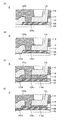
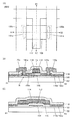
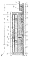
- FIG. 2 shows a structure example of a transistor.
- FIG. 2 shows a structure example of a transistor.
- 2 shows a structure example of a transistor.
- 2 shows a structure example of a transistor.
- 2 shows a structure example of a transistor.
- 2 shows a structure example of a transistor.
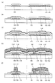
- 10A to 10D illustrate a method for manufacturing a transistor.
- 10A to 10D illustrate a method for manufacturing a transistor.
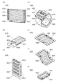
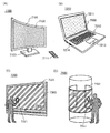
- a configuration example of a display module Configuration example of an electronic device. Configuration example of an electronic device. Configuration example of an electronic device. Configuration example of an electronic device. Calculation result of impurity element concentration.
- Cross-sectional STEM image Cross-sectional STEM image and EDX spectrum.
- Cross-sectional STEM image Cross-sectional STEM image and EDX spectrum.
- the functions of the source and drain of a transistor may be interchanged when the polarity of the transistor or the direction of current changes in circuit operation.
- the terms “source” and “drain” can be used interchangeably.
- the channel length direction of a transistor refers to one of directions parallel to a straight line connecting the source region and the drain region with the shortest distance. That is, the channel length direction corresponds to one of the directions of current flowing through the semiconductor layer when the transistor is on.
- the channel width direction is a direction orthogonal to the channel length direction. Note that depending on the structure and shape of the transistor, the channel length direction and the channel width direction may not be determined as one.
- “electrically connected” includes a case of being connected via “something having an electric action”.
- the “thing having some electric action” is not particularly limited as long as it can exchange electric signals between connection targets.
- “thing having some electric action” includes electrodes, wiring, switching elements such as transistors, resistance elements, inductors, capacitors, and other elements having various functions.
- film and “layer” can be interchanged.
- conductive layer and “insulating layer” may be interchangeable with the terms “conductive film” and “insulating film”.
- off-state current refers to drain current when a transistor is off (also referred to as a non-conduction state or a cutoff state).
- the off state is a state where the voltage V gs between the gate and the source is lower than the threshold voltage V th in the n-channel transistor (in the case of the p-channel transistor, higher than V th ) unless otherwise specified.
- a display panel which is one embodiment of a display device has a function of displaying (outputting) an image or the like on a display surface. Therefore, the display panel is one mode of the output device.
- a display panel substrate is attached with a connector such as FPC (Flexible Printed Circuit) or TCP (Tape Carrier Package), or the substrate is integrated with a COG (Chip On Glass) method.
- a connector such as FPC (Flexible Printed Circuit) or TCP (Tape Carrier Package)
- COG Chip On Glass
- a display panel module is mounted with a connector such as FPC (Flexible Printed Circuit) or TCP (Tape Carrier Package)
- COG Chip On Glass
- the touch panel which is one embodiment of the display device has a function of displaying an image or the like on the display surface, and a touched object such as a finger or a stylus touching, pressing, or approaching the display surface. And a function as a touch sensor to detect. Accordingly, the touch panel is an embodiment of an input / output device.
- the touch panel can also be called, for example, a display panel with a touch sensor (or display device) or a display panel with a touch sensor function (or display device).
- the touch panel can be configured to include a display panel and a touch sensor panel.
- the display panel may have a function as a touch sensor inside or on the surface.
- a connector or IC mounted on a touch panel substrate may be referred to as a touch panel module, a display module, or simply a touch panel.
- a semiconductor layer in which a channel is formed over a formation surface a gate insulating layer (also referred to as a first insulating layer) over the semiconductor layer, and a gate electrode over the gate insulating layer And a conductive layer.
- a protective insulating layer also referred to as a second insulating layer with a high barrier property against oxygen be provided over the semiconductor layer.
- the gate insulating layer is preferably provided in contact with the upper surface of the semiconductor layer processed into an island shape.
- the gate insulating layer preferably contains an oxide.
- the semiconductor layer preferably includes a metal oxide exhibiting semiconductor characteristics (hereinafter also referred to as an oxide semiconductor).
- the semiconductor layer includes a channel formation region where a channel can be formed and a pair of low resistance regions functioning as a source region and a drain region.
- the channel formation region is a region overlapping with the gate electrode in the semiconductor layer.
- the pair of low resistance regions are provided with the channel formation region interposed therebetween and are regions having lower resistance than the channel formation region.
- the low resistance region is preferably in contact with the second insulating layer, and the low resistance region is preferably covered with the second insulating layer.
- the second insulating layer preferably contains an impurity element.
- an impurity element hydrogen, boron, carbon, nitrogen, fluorine, phosphorus, sulfur, arsenic, aluminum, magnesium, silicon, or a rare gas can be given.
- rare gases include helium, neon, argon, krypton, and xenon.
- an impurity element refers to an element other than the main component, and an element contained by 1 atomic% or more is the main component.
- the second insulating layer preferably contains an impurity element that easily binds to oxygen.
- an impurity element that easily binds to oxygen.
- boron, phosphorus, aluminum, magnesium, silicon and the like can be mentioned.
- the second insulating layer is in contact with the low resistance region, and the second insulating layer covers the low resistance region. As a result, supply of oxygen from the second insulating layer to the low resistance region is suppressed, and the low resistance region can maintain a low electrical resistance state. In addition, supply of oxygen from the second insulating layer to the gate electrode is suppressed, and the gate electrode can maintain a low electrical resistance state.
- the second insulating layer is in contact with the side surface of the gate insulating layer, and the second insulating layer covers the gate insulating layer.
- the supply of oxygen from the gate insulating layer to the low resistance region and the gate electrode is suppressed, and the electrical resistance of the low resistance region and the gate electrode can be maintained low.
- desorption of oxygen contained in the gate insulating layer to the second insulating layer side is suppressed, so that oxygen released from the gate insulating layer can be efficiently supplied to the channel formation region of the semiconductor layer. Accordingly, oxygen vacancies in the channel formation region of the semiconductor layer can be compensated, and a highly reliable transistor can be realized.
- FIG. 1A is a top view of the transistor 100
- FIG. 1B corresponds to a cross-sectional view of a cross-sectional view taken along dashed-dotted line A1-A2 in FIG. 1A
- FIG. 1 corresponds to a cross-sectional view of a cut surface taken along one-dot chain line B1-B2 shown in FIG.
- FIG. 1A some components (such as a gate insulating layer) of the transistor 100 are omitted.
- the direction of the alternate long and short dash line A1-A2 corresponds to the channel length direction
- the direction of the alternate long and short dash line B1-B2 corresponds to the channel width direction.
- the top view of the transistor in the subsequent drawings, as in FIG. 1A, some of the components are omitted.
- the transistor 100 is provided over a substrate 102 and includes an insulating layer 103, a semiconductor layer 108, an insulating layer 110, a metal oxide layer 114, a conductive layer 112, an insulating layer 118, and the like.
- the island-shaped semiconductor layer 108 is provided over the insulating layer 103.
- the insulating layer 110 is provided in contact with part of the upper surface of the semiconductor layer 108.
- the metal oxide layer 114 and the conductive layer 112 are provided in this order on the insulating layer 110 and overlap with the semiconductor layer 108.
- the insulating layer 118 is provided to cover a part and side surfaces of the upper surface of the semiconductor layer 108, the side surfaces of the insulating layer 110, the side surfaces of the metal oxide layer 114, and the upper and side surfaces of the conductive layer 112.
- the insulating layer 118 functions as a protective layer that protects the transistor 100.
- Part of the conductive layer 112 functions as a gate electrode.
- a part of the insulating layer 110 functions as a gate insulating layer.
- the transistor 100 is a so-called top gate transistor in which a gate electrode is provided over the semiconductor layer 108.
- the semiconductor layer 108 preferably contains a metal oxide.
- the semiconductor layer 108 includes indium, M (M is gallium, aluminum, silicon, boron, yttrium, tin, copper, vanadium, beryllium, titanium, iron, nickel, germanium, zirconium, molybdenum, lanthanum, cerium, neodymium, One or more selected from hafnium, tantalum, tungsten, or magnesium) and zinc are preferable.
- M is preferably one or more selected from aluminum, gallium, yttrium, or tin.
- an oxide containing indium, gallium, and zinc is preferably used as the semiconductor layer 108.
- the semiconductor layer 108 may have a stacked structure in which layers having different compositions, layers having different crystallinity, or layers having different impurity concentrations are stacked.
- the semiconductor layer 108 includes a region overlapping with the conductive layer 112 and a pair of low resistance regions 108n sandwiching the region.
- a region of the semiconductor layer 108 that overlaps with the conductive layer 112 functions as a channel formation region of the transistor 100.
- the region 108n functions as a source region or a drain region of the transistor 100.
- the region 108n can also be referred to as a region having a lower resistance than the channel formation region, a region having a high carrier density, a region having a high oxygen deficiency density, or a region of n-type.
- the region 108n can be formed, for example, by exposing a metal oxide to plasma.
- defects typically oxygen vacancies (hereinafter sometimes referred to as V 2 O ) are generated in the metal oxide.
- V 2 O 3 oxygen vacancies
- V O H a state in which hydrogen is contained in the oxygen vacancies
- the region 108n can be formed in a self-aligned manner together with the formation of the insulating layer 118.
- the region 108n is in contact with the insulating layer 118 and the region 108n is covered with the insulating layer 118.
- the insulating layer 118 includes an oxide.
- an inorganic insulating material such as silicon oxide, silicon oxynitride, silicon nitride oxide, aluminum oxide, aluminum oxynitride, hafnium oxide, or hafnium aluminate can be used.
- the insulating layer 118 preferably further contains an impurity element.
- the impurity element include hydrogen, boron, carbon, nitrogen, fluorine, phosphorus, sulfur, arsenic, aluminum, magnesium, silicon, and a rare gas. Note that typical examples of rare gases include helium, neon, argon, krypton, and xenon.
- the insulating layer 118 particularly preferably contains an impurity element that easily binds to oxygen, and for example, preferably contains one or more selected from phosphorus, boron, magnesium, aluminum, and silicon. Further, two or more of these impurity elements may be included.
- oxynitride refers to a substance having a higher oxygen content than nitrogen as its composition.
- a nitrided oxide refers to a substance having a higher nitrogen content than oxygen as its composition.
- the insulating layer 118 includes the above-described impurity element, release of oxygen from the insulating layer 118 from the insulating layer 118 can be suppressed.
- the insulating layer 118 particularly preferably contains an impurity element that is easily bonded to oxygen. When the impurity element is bonded to oxygen in the insulating layer 118, oxygen in the insulating layer 118 is released from the insulating layer 118. It can be suppressed efficiently.
- oxygen is released from the insulating layer containing oxygen.
- oxygen is desorbed as water molecules robbing hydrogen from V O H having a region 108n (H 2 O), the V O H in which a hydrogen is deprived of oxygen vacancies (V O ).
- oxygen vacancies (Vo) generated by the removal of hydrogen from V O H are filled with another oxygen that has reached the region 108n.
- V O H and oxygen vacancies (V O ) included in the region 108n are decreased, that is, the carrier density in the region 108n is decreased, and the resistance of the region 108n may be increased.
- the insulating layer 118 in contact with the region 108n includes the above-described impurity element. With such a structure, oxygen contained in the insulating layer 118 can be prevented from being released from the insulating layer 118, and the resistance of the region 108n can be prevented from increasing.
- the insulating layer 110 has a region in contact with the channel formation region of the semiconductor layer 108, that is, a region overlapping with the conductive layer 112.
- An oxide film is preferably used for the insulating layers 103 and 110 in contact with the channel formation region of the semiconductor layer 108.
- an oxide film such as a silicon oxide film, a silicon oxynitride film, or an aluminum oxide film can be used. Accordingly, oxygen released from the insulating layer 103 or the insulating layer 110 can be supplied to the channel formation region by heat treatment or the like in the manufacturing process of the transistor 100, so that oxygen vacancies in the channel formation region can be reduced.
- the side surface of the insulating layer 110 is preferably in contact with the insulating layer 118.
- V O H and oxygen vacancies (V O ) included in the region 108n are decreased, and the resistance of the region 108n is increased.
- the conductive layer 112 is oxidized, and the resistance of the conductive layer 112 may increase.
- the side surface of the insulating layer 110 is in contact with the insulating layer 118, and the insulating layer 110 is covered with the insulating layer 118.
- the transistor 100 may include a conductive layer 120a and a conductive layer 120b over the insulating layer 118.
- the conductive layer 120a and the conductive layer 120b function as a source electrode or a drain electrode.
- the conductive layer 120a and the conductive layer 120b are electrically connected to the region 108n included in the semiconductor layer 108 through the opening 141a or the opening 141b provided in the insulating layer 118, respectively.
- the conductive layer 112, the metal oxide layer 114, and the insulating layer 110 are processed so that the upper surface shapes thereof are approximately the same.
- the top surface shape is approximately the same” means that at least a part of the contour overlaps between the stacked layers.
- the case where the upper layer and the lower layer are processed by the same mask pattern or a part thereof by the same mask pattern is included.
- the contours do not overlap, and the upper layer may be located inside the lower layer, or the upper layer may be located outside the lower layer.
- the metal oxide layer 114 positioned between the insulating layer 110 and the conductive layer 112 functions as a barrier film that prevents oxygen contained in the insulating layer 110 from diffusing to the conductive layer 112 side. Further, the metal oxide layer 114 also functions as a barrier film that prevents hydrogen and water contained in the conductive layer 112 from diffusing to the insulating layer 110 side.
- a material that hardly transmits oxygen and hydrogen more than the insulating layer 110 can be used.
- the metal oxide layer 114 can prevent oxygen from diffusing from the insulating layer 110 to the conductive layer 112 even when a metal material that easily absorbs oxygen, such as aluminum or copper, is used for the conductive layer 112. . Further, even when the conductive layer 112 contains hydrogen or water, diffusion of hydrogen or water from the conductive layer 112 to the semiconductor layer 108 through the insulating layer 110 can be prevented. As a result, the carrier density in the channel formation region of the semiconductor layer 108 can be extremely low.
- the metal oxide layer 114 an insulating material or a conductive material can be used. In the case where the metal oxide layer 114 has an insulating property, it functions as part of the gate insulating layer. On the other hand, when the metal oxide layer 114 has conductivity, it functions as a part of the gate electrode.
- an insulating material having a dielectric constant higher than that of silicon oxide is preferably used.
- an aluminum oxide film, a hafnium oxide film, a hafnium aluminate film, or the like is preferably used because the driving voltage can be reduced.
- a conductive oxide such as indium oxide, indium tin oxide (ITO), or indium tin oxide containing silicon (ITSO) can be used.
- ITO indium tin oxide
- ITSO indium tin oxide containing silicon
- a conductive oxide containing indium is preferable because of its high conductivity.
- an oxide material containing one or more of the same elements as the semiconductor layer 108 is preferably used.
- an oxide semiconductor material that can be used for the semiconductor layer 108 is preferably used.
- a metal oxide film formed using the same sputtering target as that of the semiconductor layer 108 is preferably used as the metal oxide layer 114 because the device can be used in common.
- a material having a higher gallium composition (content ratio) than the semiconductor layer 108 is used for the metal oxide layer 114.
- the barrier property against oxygen can be further improved.
- the field effect mobility of the transistor 100 can be increased by using a material whose indium composition is higher than that of the metal oxide layer 114 for the semiconductor layer 108.
- the metal oxide layer 114 is preferably formed using a sputtering apparatus.
- oxygen can be preferably added to the insulating layer 110 and the semiconductor layer 108 by being formed in an atmosphere containing oxygen gas.
- FIG. 2A shows an enlarged cross-sectional view of a region P surrounded by a one-dot chain line in FIG.
- the semiconductor layer 108 has a region 108n in contact with the insulating layer 118.
- the region 108n does not overlap with the conductive layer 112.
- the side surface of the insulating layer 110 is in contact with the insulating layer 118.
- the insulating layer 118 has an impurity element concentration of 1 ⁇ 10 19 atoms / cm 3 or more, 1 ⁇ 10 23 atoms / cm 3 or less, preferably 5 ⁇ 10 19 atoms / cm 3 or more, 5 ⁇ 10 22 atoms / cm 3. It is preferable to include a region that is 3 or less, more preferably 1 ⁇ 10 20 atoms / cm 3 or more and 1 ⁇ 10 22 atoms / cm 3 or less.
- the concentration of the impurity element contained in the insulating layer 118 is analyzed by an analysis method such as secondary ion mass spectrometry (SIMS) or X-ray photoelectron spectroscopy (XPS). be able to.
- SIMS secondary ion mass spectrometry
- XPS X-ray photoelectron spectroscopy
- concentration distribution in the depth direction can be known by combining ion sputtering from the front side or the back side and XPS analysis.
- the impurity element is preferably present in an oxidized state.
- an easily oxidizable element such as boron, phosphorus, magnesium, aluminum, or silicon as the impurity element.
- Such an easily oxidizable element can exist stably in a state where it is combined with oxygen in the insulating layer 118, and thus a high temperature (eg, 400 ° C. or higher, 600 ° C. or higher, or 800 ° C. or higher) is applied in a later step. Even in this case, desorption is suppressed.
- the impurity element when the impurity element is combined with oxygen in the insulating layer 118, release of oxygen from the insulating layer 118 from the insulating layer 118 can be suppressed.
- the insulating layer 118 containing the oxidized impurity element since the insulating layer 118 containing the oxidized impurity element is in a state where oxygen is difficult to diffuse, oxygen is supplied from outside the insulating layer 118 to the region 108n and the conductive layer 112 through the insulating layer 118. Can also be prevented. Therefore, when a treatment at a high temperature is performed, the treatment is preferably performed with the insulating layer 118 having a high barrier property against oxygen covering the region 108n and the conductive layer 112.
- boron contained in the insulating layer 118 can exist in a state of being bonded to oxygen. This can be confirmed by observing a spectral peak due to, for example, B 2 O 3 bonding in XPS analysis. Further, in XPS analysis, the peak intensity becomes extremely small to such an extent that a spectrum peak due to the state in which boron element exists alone is not observed or is buried in the background noise at the lower limit of measurement.
- Oxygen vacancies formed in the channel formation region of the semiconductor layer 108 are problematic because they affect transistor characteristics. For example, when an oxygen vacancy is formed in the channel formation region, hydrogen is bonded to the oxygen vacancy and can serve as a carrier supply source. When a carrier supply source is generated in the channel formation region, a change in electrical characteristics of the transistor 100, typically, a threshold voltage shift occurs. Therefore, the smaller the number of oxygen vacancies in the channel formation region, the better.
- the insulating film in the vicinity of the channel formation region of the semiconductor layer 108 specifically, the insulating layer 110 located above the channel formation region and the insulating layer 103 located below the oxide film It is the structure containing.
- an insulating layer 118 having a high barrier property against oxygen is in contact with a side surface of the insulating layer 110 and covers the insulating layer 110.
- oxygen that can be released from the insulating layer 110 can be prevented from diffusing to the insulating layer 118 side, and oxygen vacancies in the channel formation region of the semiconductor layer 108 can be efficiently reduced. It becomes possible.
- the semiconductor layer 108 preferably has a region in which the atomic ratio of In is larger than the atomic ratio of M. As the In atomic ratio increases, the field-effect mobility of the transistor can be improved.
- a very large amount of oxygen can be supplied into the semiconductor layer 108 containing a metal oxide, so that a metal oxide material having a large atomic ratio of In can be used.
- a transistor having extremely high field effect mobility, stable electrical characteristics, and high reliability can be realized.
- a metal oxide in which the atomic ratio of In is 1.5 times or more, or 2 times or more, or 3 times or more, or 3.5 times or more, or 4 times or more of the atomic ratio of M can be preferably used.
- a display device with a narrow frame width (also referred to as a narrow frame) can be provided by using the above-described transistor with high field-effect mobility for a gate driver that generates a gate signal.
- a gate driver that generates a gate signal.
- the transistor with high field-effect mobility described above for a source driver particularly, a demultiplexer connected to an output terminal of a shift register included in the source driver
- a display with a small number of wirings connected to a display device can be obtained.
- An apparatus can be provided.
- the crystallinity of the semiconductor layer 108 can be analyzed by, for example, analyzing using X-ray diffraction (XRD: X-Ray Diffraction), or analyzing using a transmission electron microscope (TEM). .
- XRD X-ray diffraction
- TEM transmission electron microscope
- impurities such as hydrogen or moisture mixed in the semiconductor layer 108 are problematic because they affect the transistor characteristics. Therefore, it is preferable that the semiconductor layer 108 have fewer impurities such as hydrogen or moisture.
- the use of a metal oxide film with a low impurity concentration and a low density of defect states is preferable because a transistor having excellent electrical characteristics can be manufactured. When the impurity concentration is low and the defect level density is low (oxygen vacancies are reduced), the carrier density in the film can be reduced.
- a transistor in which such a metal oxide film is used for a semiconductor layer rarely has electrical characteristics (also referred to as normally-on) in which the threshold voltage is negative.
- a transistor including such a metal oxide film can obtain characteristics with extremely low off-state current.
- a metal oxide film having a CAAC (c-axis aligned crystal) structure, a metal oxide film having an nc (nano crystal) structure, or a metal oxide in which a CAAC structure and an nc structure are mixed is used. It is preferable to use a membrane.
- the semiconductor layer 108 may have a stacked structure of two or more layers.
- the semiconductor layer 108 in which two or more metal oxide films having different compositions are stacked can be used.
- the semiconductor layer 108 in which two or more metal oxide films having different crystallinity are stacked can be used.
- the same oxide target is used and the film formation conditions are different so that the film is continuously formed without being exposed to the atmosphere.
- the semiconductor layer 108 can have a stacked structure of a metal oxide film having an nc structure and a metal oxide film having a CAAC structure.
- a stacked structure of a metal oxide film having an nc structure and a metal oxide film having an nc structure may be used.
- a CAC (Cloud-Aligned Composite) described later can be used as a function or a material structure of a metal oxide that can be preferably used for the semiconductor layer 108a and the semiconductor layer 108b.
- the oxygen flow rate ratio at the time of forming the first metal oxide film formed first is made smaller than the oxygen flow rate ratio at the time of forming the second metal oxide film formed later.
- oxygen is not allowed to flow when the first metal oxide film is formed.
- oxygen can be effectively supplied when forming the second metal oxide film.
- the first metal oxide film can be a film having lower crystallinity and higher electrical conductivity than the second metal oxide film.
- the second metal oxide film provided on the top is a film having higher crystallinity than the first metal oxide film, so that damage during the processing of the semiconductor layer 108 or the film formation of the insulating layer 110 is caused. Can be suppressed.
- the oxygen flow rate ratio during the formation of the first metal oxide film is 0% or more and less than 50%, preferably 0% or more and 30% or less, more preferably 0% or more and 20% or less. Specifically, it is 10%.
- the oxygen flow rate ratio during the formation of the second metal oxide film is 50% to 100%, preferably 60% to 100%, more preferably 80% to 100%, and still more preferably 90% or more. 100% or less, typically 100%.
- the first metal oxide film and the second metal oxide film may have different conditions such as pressure, temperature, and power at the time of film formation, but the conditions other than the oxygen flow rate ratio are the same. This is preferable because the time required for the film forming process can be shortened.
- the transistor 100 having excellent electrical characteristics and high reliability can be realized.
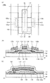
- FIG. 3A is a top view of the transistor 100A
- FIG. 3B is a cross-sectional view in the channel length direction of the transistor 100A
- FIG. 3C is a cross-sectional view in the channel width direction of the transistor 100A. .
- the transistor 100A is mainly different from the transistor 100 in that the region 108n includes the impurity element described above.
- the insulating layer 103 may have a region 103 d containing the above-described impurity element in the vicinity of the interface in contact with the insulating layer 118. Further, the region 103d may be provided in the vicinity of the interface in contact with the region 108n. At this time, the impurity concentration in a portion overlapping with the region 108n may be lower than that in a portion in contact with the insulating layer 118.
- the region 103 d can be formed by performing heat treatment after forming the insulating layer 118 and diffusing the impurity element included in the insulating layer 118 into the insulating layer 103. Further, the impurity element included in the insulating layer 118 is diffused into the semiconductor layer 108 by the heat treatment, so that the region 108n containing the impurity element can be formed. Accordingly, the region 110d can be formed in a self-aligned manner simultaneously with the formation of the region 108n containing the impurity element. In the transistor 100A, the region 108n can also be referred to as a region having a higher impurity element concentration than the channel formation region. Note that when the insulating layer 118 is formed, the region 108n and the region 103d containing an impurity element may be formed.
- FIG. 2B shows an enlarged cross-sectional view of a region Q surrounded by a one-dot chain line in FIG.
- the impurity element in the region 108n preferably has a concentration gradient such that the concentration becomes higher as the region 108n is closer to the insulating layer 118. Accordingly, the upper portion of the region 108n has a lower resistance, so that the contact resistance with the conductive layer 120a (or the conductive layer 120b) can be more effectively reduced.
- the concentration of the impurity element in the region 108n can be adjusted by the formation conditions of the insulating layer 118 and the temperature and time of heat treatment performed after the insulating layer 118 is formed.
- the region 103 d is formed in the insulating layer 103 in order to exaggerately indicate that the high impurity element concentration portion of the insulating layer 103 is located in the vicinity of the interface with the insulating layer 118.
- the hatching pattern is shown only in the vicinity of the insulating layer 118, the impurity element may actually be included over the entire thickness direction of the insulating layer 103.
- Each of the region 108n and the region 103d has an impurity concentration of 1 ⁇ 10 19 atoms / cm 3 or more, 1 ⁇ 10 23 atoms / cm 3 or less, preferably 5 ⁇ 10 19 atoms / cm 3 or more, and 5 ⁇ 10 22 atoms / cm 3. It is preferable to include a region of cm 3 or less, more preferably 1 ⁇ 10 20 atoms / cm 3 or more and 1 ⁇ 10 22 atoms / cm 3 or less.
- the concentration of impurities contained in the region 108n and the region 103d can be analyzed by an analysis method such as secondary ion mass spectrometry (SIMS) or X-ray photoelectron spectroscopy (XPS).
- SIMS secondary ion mass spectrometry
- XPS X-ray photoelectron spectroscopy
- concentration distribution in the depth direction can be known by combining ion sputtering from the front side or the back side and XPS analysis.
- the impurity element is preferably present in an oxidized state.
- an easily oxidizable element such as boron, phosphorus, magnesium, aluminum, or silicon
- Such an easily oxidizable element can exist stably in a state where it is combined with oxygen in the semiconductor layer 108, so that a high temperature (eg, 400 ° C. or higher, 600 ° C. or higher, or 800 ° C. or higher) is applied in a later step. Even in this case, desorption is suppressed.
- the impurity element deprives oxygen in the semiconductor layer 108, many oxygen vacancies (V 2 O 3 ) are generated in the region 108n.
- V O H in which this oxygen deficiency (V 2 O 3 ) and hydrogen in the film are combined, the carrier density is increased and the region 108 n is in a very low resistance state.
- the treatment is preferably performed in a state of being covered with an insulating layer 118 having a high barrier property against oxygen.
- the impurity element is preferably present in an oxidized state.
- Such an easily oxidizable element can exist stably in a state of being bonded to oxygen in the insulating layer 103, and thus desorption is suppressed even when a high temperature is applied in a later step.
- the insulating layer 103 contains oxygen that can be desorbed by heating (also referred to as excess oxygen)
- the excess oxygen and the impurity element are combined and stabilized, so that oxygen flows from the region 103d to the region 108n. Supplying can be suppressed.
- the region 103d containing the oxidized impurity element is in a state in which oxygen is difficult to diffuse, oxygen can be prevented from being supplied to the region 108n through the region 103d from above the region 103d. Can do.
- boron contained in the region 108n and the region 103d can exist in a state of being bonded to oxygen. This can be confirmed by observing a spectrum peak due to the B 2 O 3 bond in the XPS analysis. Further, in XPS analysis, the peak intensity becomes extremely small to such an extent that a spectrum peak due to the state in which boron element exists alone is not observed or is buried in the background noise at the lower limit of measurement.
- the region 103d may be provided near the interface in contact with the region 108n. At this time, the impurity concentration of the portion overlapping with the region 108 n is lower than that of the portion in contact with the insulating layer 110.
- FIG. 4A is a top view of the transistor 100B
- FIG. 4B is a cross-sectional view in the channel length direction of the transistor 100B
- FIG. 4C is a cross-sectional view in the channel width direction of the transistor 100B. .
- the transistor 100B is mainly different from the configuration example 1 in that the insulating layer 110 is formed by extending over the region 108n and the insulating layer 103.
- the insulating layer 110 includes a top surface and a side surface of the semiconductor layer 108 and a region which is in contact with the top surface of the insulating layer 103 and does not overlap with the conductive layer 112.
- FIG. 2C shows an enlarged cross-sectional view of a region R surrounded by a dashed line in FIG. 4B.
- the region 108n may include the above-described impurity element.
- the impurity element it is preferable that the impurity element have a concentration gradient such that the concentration is higher as the insulating element is closer to the insulating layer 110. Accordingly, the upper portion of the region 108n has a lower resistance, so that the contact resistance with the conductive layer 120a (or the conductive layer 120b) can be more effectively reduced.
- the concentration of the impurity element in the region 108n can be adjusted by the thickness of the insulating layer 110, the formation conditions of the insulating layer 118, and the temperature and time of heat treatment performed after the insulating layer 118 is formed.
- the insulating layer 110 has a region 108 n and a region 110 d in contact with the insulating layer 103.
- the region 110d contains the impurity element described above.
- the region 110d is preferably not provided in a portion in contact with the channel formation region of the semiconductor layer 108.
- the above-described impurity element region 110d can suppress release of oxygen compared to other regions. Therefore, the region 110d functions as a barrier layer against oxygen, and oxygen supplied to the region 108n can be effectively reduced.
- the region 110 d can be formed by performing heat treatment after the insulating layer 118 is formed and diffusing the impurity element included in the insulating layer 118 into the insulating layer 110. Further, the impurity element diffuses into the semiconductor layer 108 by the heat treatment, so that the region 108n can contain the impurity element.
- the region 110d has an impurity concentration of 1 ⁇ 10 19 atoms / cm 3 or more, 1 ⁇ 10 23 atoms / cm 3 or less, preferably 5 ⁇ 10 19 atoms / cm 3 or more, and 5 ⁇ 10 22 atoms / cm 3 or less. It is preferable to include a region that is preferably 1 ⁇ 10 20 atoms / cm 3 or more and 1 ⁇ 10 22 atoms / cm 3 or less.
- the region 108n preferably includes a portion with a higher impurity concentration than the region 110d of the insulating layer 110, because the electric resistance of the region 108n can be reduced more effectively.
- the concentration of impurities contained in the region 110d can be analyzed by an analysis method such as secondary ion mass spectrometry (SIMS) or X-ray photoelectron spectroscopy (XPS).
- SIMS secondary ion mass spectrometry
- XPS X-ray photoelectron spectroscopy
- concentration distribution in the depth direction can be known by combining ion sputtering from the front side or the back side and XPS analysis.
- the impurity element is preferably present in an oxidized state.
- an easily oxidizable element such as boron, phosphorus, magnesium, aluminum, or silicon as the impurity element.
- Such an easily oxidizable element can exist stably in a state where it is combined with oxygen in the insulating layer 110, and thus desorption is suppressed even when a high temperature is applied in a later step.
- oxygen that can be released by heating also referred to as excess oxygen
- excess oxygen and the impurity element are combined and stabilized, so that oxygen is transferred from the region 110d to the region 108n. Supplying can be suppressed.
- the region 110d containing the oxidized impurity element is in a state in which oxygen is difficult to diffuse, oxygen is prevented from being supplied to the region 108n through the region 110d from above the region 110d. Can do.
- boron contained in the region 110d can exist in a state of being bonded to oxygen. This can be confirmed by observing a spectrum peak due to the B 2 O 3 bond in the XPS analysis. Further, in XPS analysis, the peak intensity becomes extremely small to such an extent that a spectrum peak due to the state in which boron element exists alone is not observed or is buried in the background noise at the lower limit of measurement.
- the insulating layer 103 may have a region 103 d containing the above-described impurity element in the vicinity of the interface in contact with the insulating layer 110. Further, the region 103d may be provided in the vicinity of the interface in contact with the region 108n. At this time, the impurity concentration of the portion overlapping with the region 108 n is lower than that of the portion in contact with the insulating layer 110.
- FIG. 5A is a top view of the transistor 100C
- FIG. 5B is a cross-sectional view in the channel length direction of the transistor 100C
- FIG. 5C is a cross-sectional view in the channel width direction of the transistor 100C. .
- the transistor 100C is mainly different from the transistor 100B in that the insulating layer 110 has regions having different film thicknesses.
- FIG. 2D shows an enlarged cross-sectional view of a region S surrounded by a one-dot chain line in FIG.
- the thickness of the insulating layer 110 in the region that does not overlap with the conductive layer 112, that is, the region 110d is smaller than the thickness of the insulating layer 110 in the region that overlaps with the conductive layer 112.
- the distance between the insulating layer 118 and the region 108n is shortened, and the impurity concentration in the region 108n can be increased.
- the concentration of the impurity element in the region 108n can be easily adjusted.
- the concentration of the impurity element in the region 108n can be adjusted by the temperature and time of heat treatment performed after the insulating layer 118 is formed.
- FIG. 6A is a top view of the transistor 100D
- FIG. 6B is a cross-sectional view in the channel length direction of the transistor 100D
- FIG. 6C is a cross-sectional view in the channel width direction of the transistor 100D. .
- the transistor 100D is mainly different from the transistor 100 in that the conductive layer 106 is provided between the substrate 102 and the insulating layer 103.
- the conductive layer 106 has a region overlapping with the semiconductor layer 108 and the conductive layer 112.
- FIG. 7A is a top view of the transistor 100E
- FIG. 7B is a cross-sectional view in the channel length direction of the transistor 100E
- FIG. 7C is a cross-sectional view in the channel width direction of the transistor 100E. .
- the transistor 100E is mainly different from the transistor 100C in that the conductive layer 106 is provided between the substrate 102 and the insulating layer 103.
- the conductive layer 106 has a region overlapping with the semiconductor layer 108 and the conductive layer 112.
- the conductive layer 106 functions as a first gate electrode (also referred to as a bottom gate electrode), and the conductive layer 112 serves as a second gate electrode (also referred to as a top gate electrode). It has a function.
- a part of the insulating layer 103 functions as a first gate insulating layer, and a part of the insulating layer 110 functions as a second gate insulating layer.
- a portion of the semiconductor layer 108 overlapping with at least one of the conductive layer 112 and the conductive layer 106 functions as a channel formation region. Note that a portion overlapping with the conductive layer 112 of the semiconductor layer 108 is sometimes referred to as a channel formation region for ease of explanation below, but actually overlaps with the conductive layer 106 without overlapping with the conductive layer 112. A channel can also be formed in a portion (a portion including the region 108n).
- the conductive layer 106 includes a metal oxide layer 114, an insulating layer 110, and an opening 142 provided in the insulating layer 103 through the opening 142. 112 may be electrically connected. Accordingly, the same potential can be applied to the conductive layer 106 and the conductive layer 112.
- the conductive layer 106 can be formed using a material similar to that of the conductive layer 112, the conductive layer 120a, or the conductive layer 120b. In particular, it is preferable to use a material containing copper for the conductive layer 106 because wiring resistance can be reduced.
- the conductive layer 112 and the conductive layer 106 are end portions of the semiconductor layer 108 in the channel width direction. It is preferable to protrude outward. At this time, as illustrated in FIGS. 6C and 7C, the entire semiconductor layer 108 in the channel width direction is covered with the conductive layer 112 and the conductive layer 106 with the insulating layer 110 and the insulating layer 103 interposed therebetween. It becomes a broken structure.
- the semiconductor layer 108 can be electrically surrounded by an electric field generated by the pair of gate electrodes. At this time, it is particularly preferable to apply the same potential to the conductive layer 106 and the conductive layer 112. Accordingly, an electric field for inducing a channel can be effectively applied to the semiconductor layer 108, so that the on-state current of the transistor 100D and the transistor 100E can be increased. Therefore, the transistor 100D and the transistor 100E can be miniaturized.
- the conductive layer 112 and the conductive layer 106 may not be connected. At this time, a constant potential may be applied to one of the pair of gate electrodes, and a signal for driving the transistor 100D and the transistor 100E may be applied to the other. At this time, the threshold voltage when the transistor 100D and the transistor 100E are driven by the other electrode can be controlled by the potential applied to the one electrode.
- the capacitor 130A is provided side by side with the transistor 100 illustrated in Structural Example 1.
- the capacitor 130A is provided side by side with the transistor 100D illustrated in Structural Example 3.
- the capacitor 130A has a structure in which an insulating layer 110 that functions as a dielectric and an insulating layer 118 are provided between the semiconductor layer 108c and the conductive layer 120b.
- the semiconductor layer 108 c is provided on the same surface as the semiconductor layer 108.
- the semiconductor layer 108c can be formed by processing the same metal oxide film as the semiconductor layer 108 and then adding the same impurity element as the region 108n.
- the capacitor element 130A can be manufactured without increasing the number of steps.
- a capacitor 130B illustrated in FIG. 8C has a structure in which the insulating layer 103 functioning as a dielectric is provided between the conductive layer 106c and the semiconductor layer 108c.
- the conductive layer 106 c is provided on the same plane as the conductive layer 106.
- the conductive layer 106 c can be formed by processing the same conductive film as the conductive layer 106.
- the capacitor element 130B can be made to have a larger capacity because the thickness of the dielectric can be made thinner than that of the capacitor element 130A.
- the substrate 102 there is no particular limitation on the material of the substrate 102, but it is necessary that the substrate 102 have at least heat resistance to withstand heat treatment performed later.
- a single crystal semiconductor substrate made of silicon or silicon carbide, a polycrystalline semiconductor substrate, a compound semiconductor substrate such as silicon germanium, an SOI substrate, a glass substrate, a ceramic substrate, a quartz substrate, a sapphire substrate, or the like is used as the substrate 102. Also good.
- a substrate in which a semiconductor element is provided over these substrates may be used as the substrate 102.
- a flexible substrate may be used as the substrate 102, and the transistor 100 or the like may be formed directly over the flexible substrate.
- a separation layer may be provided between the substrate 102 and the transistor 100 or the like. The separation layer can be used for separation from the substrate 102 and transfer to another substrate after part or all of the semiconductor device is completed thereon. At that time, the transistor 100 or the like can be transferred to a substrate having poor heat resistance or a flexible substrate.
- the insulating layer 103 can be formed using a sputtering method, a CVD method, an evaporation method, a pulsed laser deposition (PLD) method, or the like as appropriate.
- a sputtering method for example, an oxide insulating film or a nitride insulating film can be formed as a single layer or a stacked layer.
- at least a region in contact with the semiconductor layer 108 in the insulating layer 103 is preferably formed using an oxide insulating film.
- the insulating layer 103 is preferably a film that releases oxygen by heating.
- the insulating layer 103 for example, silicon oxide, silicon oxynitride, silicon nitride oxide, silicon nitride, aluminum oxide, hafnium oxide, gallium oxide, Ga—Zn oxide, or the like may be used, and the insulating layer 103 can be provided as a single layer or a stacked layer.
- the surface in contact with the semiconductor layer 108 of the insulating layer 103 is subjected to pretreatment such as oxygen plasma treatment. Or it is preferable to oxidize the vicinity of the surface.
- the conductive layer 112 and the conductive layer 106 functioning as gate electrodes, the conductive layer 120a functioning as a source electrode, and the conductive layer 120b functioning as a drain electrode include chromium, copper, aluminum, gold, silver, zinc, molybdenum, tantalum, and titanium. , Tungsten, manganese, nickel, iron, and cobalt, or an alloy containing the above-described metal element as a component, an alloy that combines the above-described metal elements, or the like.
- the conductive layer 112, the conductive layer 106, the conductive layer 120a, and the conductive layer 120b include an In—Sn oxide, an In—W oxide, an In—W—Zn oxide, an In—Ti oxide, and an In—Ti oxide.
- An oxide conductor such as -Sn oxide, In-Zn oxide, In-Sn-Si oxide, or In-Ga-Zn oxide, or a metal oxide film can also be used.
- an oxide conductor (OC: Oxide Conductor)
- OC Oxide Conductor
- a donor level is formed in the vicinity of the conduction band.
- the metal oxide becomes highly conductive and becomes a conductor.
- the conductive metal oxide can be referred to as an oxide conductor.
- the conductive layer 112 or the like may have a stacked structure of a conductive film including the oxide conductor (metal oxide) and a conductive film including a metal or an alloy.
- a conductive film including an oxide conductor is preferably applied to a side in contact with the insulating layer functioning as a gate insulating film.
- the conductive layer 112, the conductive layer 106, the conductive layer 120a, and the conductive layer 120b each include any one or more selected from titanium, tungsten, tantalum, and molybdenum among the above metal elements. Is preferred.
- the tantalum nitride film is conductive, has a high barrier property against copper, oxygen, or hydrogen, and emits less hydrogen from itself. Therefore, the conductive film in contact with the semiconductor layer 108, Alternatively, it can be preferably used as a conductive film in the vicinity of the semiconductor layer 108.
- the insulating layer 110 functioning as a gate insulating film of the transistor 100 or the like can be formed by a PECVD method, a sputtering method, or the like.
- An insulating layer including one or more of a film, a lanthanum oxide film, a cerium oxide film, and a neodymium oxide film can be used.
- the insulating layer 110 may have a two-layer structure or a three-layer structure.
- the insulating layer 110 in contact with the semiconductor layer 108 is preferably an oxide insulating film, and more preferably has a region containing oxygen in excess of the stoichiometric composition.
- the insulating layer 110 is an insulating film capable of releasing oxygen.
- the insulating layer 110 is formed in an oxygen atmosphere, the heat treatment in the oxygen atmosphere, plasma treatment, or the like is performed on the insulating layer 110 after film formation, or the oxygen layer is formed over the insulating layer 110 in an oxygen atmosphere.
- Oxygen can be supplied into the insulating layer 110 by forming an oxide film or the like.
- the insulating layer 110 a material such as hafnium oxide having a higher relative dielectric constant than silicon oxide or silicon oxynitride can be used. This increases the thickness of the insulating layer 110 and suppresses leakage current due to tunneling current.
- hafnium oxide having crystallinity is preferable because it has a higher relative dielectric constant than amorphous hafnium oxide.
- a sputtering target used for forming the In-M-Zn oxide preferably has an In atomic ratio equal to or higher than the M atomic ratio.
- the atomic ratio of the semiconductor layer 108 to be formed includes a variation of plus or minus 40% of the atomic ratio of the metal element included in the sputtering target.
- the atomic ratio of Ga is larger than 0.1 when the atomic ratio of In is 5. 2 or less, and includes the case where the atomic ratio of Zn is 5 or more and 7 or less.
- the atomic ratio of Ga is larger than 0.1 when the atomic ratio of In is 1. 2 or less, including the case where the atomic ratio of Zn is greater than 0.1 and 2 or less.
- the semiconductor layer 108 has an energy gap of 2 eV or more, preferably 2.5 eV or more. In this manner, off-state current of a transistor can be reduced by using a metal oxide having a wider energy gap than silicon.
- the semiconductor layer 108 preferably has a non-single crystal structure.
- the non-single crystal structure includes, for example, a CAAC structure, a polycrystalline structure, a microcrystalline structure, or an amorphous structure, which will be described later.
- the amorphous structure has the highest defect level density
- the CAAC structure has the lowest defect level density.
- CAAC c-axis aligned crystal
- the CAAC structure is one of crystal structures such as a thin film having a plurality of nanocrystals (a crystal region having a maximum diameter of less than 10 nm). Each nanocrystal has a c-axis oriented in a specific direction and an a-axis.
- the b-axis is a crystal structure having a feature that nanocrystals are continuously connected without forming a grain boundary without having orientation.
- a thin film having a CAAC structure has a feature that the c-axis of each nanocrystal is easily oriented in the thickness direction of the thin film, the normal direction of the surface to be formed, or the normal direction of the surface of the thin film.
- CAAC-OS Oxide Semiconductor
- CAAC-OS Oxide Semiconductor
- CAAC-OS cannot confirm a clear crystal grain boundary, it can be said that a decrease in electron mobility due to the crystal grain boundary hardly occurs.
- the CAAC-OS can be said to be an oxide semiconductor with few impurities and defects (such as oxygen vacancies). Therefore, the physical properties of the oxide semiconductor including a CAAC-OS are stable. Therefore, an oxide semiconductor including a CAAC-OS is resistant to heat and has high reliability.
- crystallography it is common to take a unit cell having a specific axis as the c-axis among the three axes (crystal axis) of the a-axis, b-axis, and c-axis constituting the unit cell.
- a crystal having a layered structure two axes parallel to the plane direction of the layer are generally defined as an a axis and a b axis, and an axis intersecting the layer is generally defined as a c axis.
- a crystal having such a layered structure there is graphite classified as a hexagonal system, the a-axis and b-axis of the unit cell are parallel to the cleavage plane, and the c-axis is orthogonal to the cleavage plane.
- graphite classified as a hexagonal system the a-axis and b-axis of the unit cell are parallel to the cleavage plane, and the c-axis is orthogonal to the cleavage plane.
- an InGaZnO 4 crystal having a layered structure of YbFe 2 O 4 type crystal structure can be classified into a hexagonal system, and the a-axis and b-axis of the unit cell are parallel to the plane direction of the layer, and the c-axis Is orthogonal to the layer (ie, the a-axis and b-axis).
- a crystal part may not be clearly observed in an observation image using a TEM.
- a crystal part included in the microcrystalline oxide semiconductor film has a size of 1 nm to 100 nm, or 1 nm to 10 nm.
- an oxide semiconductor film including nanocrystals (nc: nanocrystal) that is 1 nm to 10 nm, or 1 nm to 3 nm is referred to as an nc-OS (nanocrystalline Oxide Semiconductor) film.
- nc-OS nanocrystalline Oxide Semiconductor
- the nc-OS film has periodicity in atomic arrangement in a minute region (for example, a region of 1 nm to 10 nm, particularly a region of 1 nm to 3 nm).
- the nc-OS film does not have regularity in crystal orientation between different crystal parts. Therefore, orientation is not seen in the whole film. Therefore, the nc-OS film may not be distinguished from an amorphous oxide semiconductor film depending on an analysis method. For example, when structural analysis is performed on the nc-OS film using an XRD apparatus using X-rays having a diameter larger than that of the crystal part, a peak indicating a crystal plane is not detected in the analysis by the out-of-plane method.
- nc-OS film is subjected to electron diffraction (also referred to as nanobeam electron diffraction) using an electron beam with a probe diameter (for example, 1 nm to 30 nm) that is close to the crystal part or smaller than the crystal part. A region having a high luminance is observed so as to draw a circle (in a ring shape), and a spot in which a plurality of spots may be observed in the ring-shaped region can be observed.
- the nc-OS film has a lower density of defect states than the amorphous oxide semiconductor film. Note that the nc-OS film does not have regularity in crystal orientation between different crystal parts. Therefore, the nc-OS film has a higher density of defect states than the CAAC-OS film. Therefore, the nc-OS film has a higher carrier density and higher electron mobility than the CAAC-OS film in some cases. Therefore, a transistor including the nc-OS film may exhibit high field effect mobility.
- the nc-OS film can be formed by reducing the oxygen flow rate ratio during deposition as compared with the CAAC-OS film.
- the nc-OS film can also be formed by lowering the substrate temperature at the time of deposition as compared with the CAAC-OS film.
- the nc-OS film can be formed even when the substrate temperature is relatively low (for example, 130 ° C. or lower) or the substrate is not heated, so that a large glass substrate, a resin substrate, or the like can be used. And can increase productivity.
- the metal oxide formed by sputtering using the above target at a substrate temperature of 100 ° C. or higher and 130 ° C. or lower is a crystal structure of one of an nc (nano crystal) structure and a CAAC structure, or a structure in which these are mixed It is easy to take.
- a metal oxide formed by a sputtering method at a substrate temperature of room temperature (RT) is likely to have an nc crystal structure.
- the room temperature (RT) here includes a temperature when the substrate is not heated.
- composition of metal oxide A structure of a CAC (Cloud-Aligned Composite) -OS that can be used for the transistor disclosed in one embodiment of the present invention is described below.
- CAAC c-axis aligned crystal
- CAC Cloud-Aligned Composite
- CAC-OS or CAC-metal oxide has a conductive function in a part of the material and an insulating function in a part of the material, and the whole material has a function as a semiconductor.
- the conductive function is a function of flowing electrons (or holes) serving as carriers
- the insulating function is an electron serving as carriers. It is a function that does not flow.
- CAC-OS or CAC-metal oxide has a conductive region and an insulating region.
- the conductive region has the above-described conductive function
- the insulating region has the above-described insulating function.
- the conductive region and the insulating region may be separated at the nanoparticle level.
- the conductive region and the insulating region may be unevenly distributed in the material, respectively.
- the conductive region may be observed with the periphery blurred and connected in a cloud shape.
- the conductive region and the insulating region are dispersed in the material with a size of 0.5 nm to 10 nm, preferably 0.5 nm to 3 nm, respectively. There is.
- CAC-OS or CAC-metal oxide is composed of components having different band gaps.
- CAC-OS or CAC-metal oxide includes a component having a wide gap caused by an insulating region and a component having a narrow gap caused by a conductive region.
- the carrier when the carrier flows, the carrier mainly flows in the component having the narrow gap.
- the component having a narrow gap acts in a complementary manner to the component having a wide gap, and the carrier flows through the component having the wide gap in conjunction with the component having the narrow gap. Therefore, when the CAC-OS or the CAC-metal oxide is used for a channel formation region of a transistor, high current driving force, that is, high on-state current and high field-effect mobility can be obtained in the on-state of the transistor.
- CAC-OS or CAC-metal oxide can also be called a matrix composite material (metal matrix composite) or a metal matrix composite material (metal matrix composite).
- a thin film (insulating film, semiconductor film, conductive film, or the like) included in the semiconductor device is formed by sputtering, chemical vapor deposition (CVD), vacuum evaporation, or pulsed laser deposition (PLD: Pulsed Laser Deposition).
- CVD chemical vapor deposition
- PLD Pulsed Laser Deposition
- atomic layer deposition ALD: Atomic Layer Deposition
- CVD method include a plasma enhanced chemical vapor deposition (PECVD) method and a thermal CVD method.
- PECVD plasma enhanced chemical vapor deposition
- thermal CVD there is a metal organic chemical vapor deposition (MOCVD) method.
- Thin films (insulating films, semiconductor films, conductive films, etc.) that constitute semiconductor devices are spin coat, dip, spray coating, ink jet, dispense, screen printing, offset printing, doctor knife, slit coat, roll coat, curtain coat. It can be formed by a method such as knife coating.
- the thin film constituting the semiconductor device when processing the thin film constituting the semiconductor device, it can be processed using a photolithography method or the like.
- the thin film may be processed by a nanoimprint method, a sand blast method, a lift-off method, or the like.
- the island-shaped thin film may be directly formed by a film forming method using a shielding mask such as a metal mask.
- light used for exposure can be, for example, i-line (wavelength 365 nm), g-line (wavelength 436 nm), h-line (wavelength 405 nm), or light obtained by mixing these.
- ultraviolet light, KrF laser light, ArF laser light, or the like can be used.
- exposure may be performed by an immersion exposure technique.
- extreme ultraviolet light (EUV: Extreme-violet) or X-rays may be used as light used for exposure.
- an electron beam can be used instead of the light used for exposure. It is preferable to use extreme ultraviolet light, X-rays, or an electron beam because extremely fine processing is possible. Note that a photomask is not necessary when exposure is performed by scanning a beam such as an electron beam.
- etching the thin film For etching the thin film, a dry etching method, a wet etching method, a sand blasting method, or the like can be used.
- FIGS. 9 and 10 cross sections in the channel length direction and the channel width direction in each stage of the manufacturing process of the transistor 100D are shown side by side.
- a conductive film is formed over the substrate 102 and processed by etching, so that a conductive layer 106 functioning as a gate electrode is formed.
- an insulating layer 103 is formed so as to cover the substrate 102 and the conductive layer 106 (FIG. 9A).
- the insulating layer 103 can be formed by a PECVD method, an ALD method, a sputtering method, or the like.
- a process for supplying oxygen to the insulating layer 103 may be performed.
- plasma treatment or heat treatment in an oxygen atmosphere can be performed.
- oxygen may be supplied to the insulating layer 103 by a plasma ion doping method or an ion implantation method.
- the metal oxide film is preferably formed by a sputtering method using a metal oxide target.
- an inert gas eg, helium gas, argon gas, xenon gas, etc.
- oxygen flow ratio the ratio of oxygen gas to the entire deposition gas when forming the metal oxide film
- the lower the oxygen flow ratio the lower the crystallinity of the metal oxide film and the transistor with higher on-state current.
- the metal oxide film may be formed under conditions of a substrate temperature of room temperature to 200 ° C., preferably a substrate temperature of room temperature to 140 ° C.
- the film formation temperature be set to a room temperature or higher and lower than 140 ° C. because productivity is increased.
- crystallinity can be lowered by forming the metal oxide film with the substrate temperature set to room temperature or without heating.
- a process for desorbing water, hydrogen, organic components, or the like adsorbed on the surface of the insulating layer 103 or a process for supplying oxygen into the insulating layer 103 is performed.
- the heat treatment can be performed at a temperature of 70 ° C. or higher and 200 ° C. or lower in a reduced pressure atmosphere.
- plasma treatment in an atmosphere containing oxygen may be performed.
- organic substances on the surface of the insulating layer 103 can be preferably removed. After such treatment, it is preferable to continuously form a metal oxide film without exposing the surface of the insulating layer 103 to the atmosphere.
- one or both of a wet etching method and a dry etching method may be used. At this time, part of the insulating layer 103 that does not overlap with the semiconductor layer 108 may be etched and thinned.
- heat treatment may be performed to remove hydrogen or water in the metal oxide film or the semiconductor layer 108.
- the temperature of the heat treatment can be typically 150 ° C. or higher and lower than the strain point of the substrate, 250 ° C. or higher and 450 ° C. or lower, or 300 ° C. or higher and 450 ° C. or lower.
- the heat treatment can be performed in an atmosphere containing a rare gas or nitrogen. Alternatively, after heating in the atmosphere, heating may be performed in an atmosphere containing oxygen. Note that it is preferable that hydrogen, water, and the like be not contained in the heat treatment atmosphere.
- an electric furnace, an RTA apparatus, or the like can be used. By using the RTA apparatus, the heat treatment time can be shortened.
- an insulating film 110f to be the insulating layer 110 and a metal oxide film 114f to be the metal oxide layer 114 are stacked to cover the insulating layer 103 and the semiconductor layer 108 (FIG. 9C). .
- an oxide film such as a silicon oxide film or a silicon oxynitride film is preferably formed using a plasma chemical vapor deposition apparatus (a PECVD apparatus or simply a plasma CVD apparatus). Alternatively, a PECVD method using a microwave may be used.
- the metal oxide film 114f is preferably formed in an atmosphere containing oxygen, for example.
- it is preferably formed by a sputtering method in an atmosphere containing oxygen. Accordingly, oxygen can be supplied to the insulating film 110f when the metal oxide film 114f is formed.
- the metal oxide film 114f is formed by a sputtering method using an oxide target containing a metal oxide similar to that of the semiconductor layer 108, the above can be used.
- the metal oxide film may be formed by a reactive sputtering method using oxygen as a film forming gas and using a metal target.
- a metal target for example, an aluminum oxide film can be formed.
- the oxygen supplied into the film 110f can be increased.
- the oxygen flow rate ratio or the oxygen partial pressure is, for example, 50% to 100%, preferably 65% to 100%, more preferably 80% to 100%, and still more preferably 90% to 100%. In particular, it is preferable that the oxygen flow rate ratio is 100% and the oxygen partial pressure is as close as possible to 100%.
- oxygen may be supplied from the insulating film 110f to the semiconductor layer 108 by performing heat treatment after the metal oxide film 114f is formed.
- the heat treatment can be performed at a temperature of 200 ° C. to 400 ° C. in an atmosphere containing one or more of nitrogen, oxygen, and a rare gas.
- the metal oxide film 114f is formed, the metal oxide film 114f, the insulating film 110f, and a part of the insulating layer 103 are etched, so that an opening reaching the conductive layer 106 is formed. Accordingly, the conductive layer 112 and the conductive layer 106 to be formed later can be electrically connected through the opening.
- a conductive film 112f to be the conductive layer 112 is formed over the insulating film 110f and the metal oxide film 114f (FIG. 9D).
- the conductive film 112f is preferably formed by a sputtering method using a metal or alloy sputtering target.
- the insulating film 110f, the conductive film 112f, and a part of the metal oxide film 114f are etched to form the insulating layer 110, the conductive layer 112, and the metal oxide layer 114 (FIG. 9E).
- the insulating film 110f, the conductive film 112f, and the metal oxide film 114f are each preferably processed using the same resist mask.
- the insulating film 110f and the metal oxide film 114f may be etched using the conductive layer 112 after etching as a hard mask.
- the insulating layer 110, the conductive layer 112, and the metal oxide layer 114 having substantially the same top surface shape.
- an insulating layer 118 is formed (FIG. 10A).
- the insulating layer 118 can be formed by a CVD method such as plasma CVD, low pressure CVD, or ECRCVD.
- a gas containing an impurity element impurity element source
- impurity element source a gas containing an impurity element
- a silicon source, an oxygen source, and an impurity element source can be used as a source gas.
- a silicon source, an oxygen source, and an impurity element source can be used as a source gas.
- a silicon source, an oxygen source, a nitrogen source, and an impurity element source can be used as a source gas.
- the silicon source organic silanes such as TEOS (Tetraethyl orthosilicate), inorganic silanes such as SiH 4 (monosilane) and Si 2 H 6 (disilane) can be used.
- oxygen source O 2 , O 3 , N 2 O, or the like can be used.
- NH 3 , N 2 O, or the like can be used as the nitrogen source.
- N 2 O can be used as an oxygen source and a nitrogen source.
- phosphorus is used as the impurity element
- PH 3 (phosphine) or the like can be used as the impurity element source.
- B 2 H 6 (diborane) or the like can be used as the impurity element source. A plurality of these impurity element sources may be used.
- the entire insulating layer 118 can contain the impurity element.
- the impurity element in the entire insulating layer 118 it is possible to efficiently suppress the oxygen included in the insulating layer 118 from being detached from the insulating layer 118.
- the concentration of the impurity element in the film thickness direction of the insulating layer 118 can be made uniform.
- the ratio of the maximum value to the minimum value of the impurity concentration is preferably 1.0 or more and 10.0 or less, more preferably 1.0 or more and 7.0 or less, and further 1.0 or more. 5.0 or less is preferable, and 1.0 or more and 3.0 or less are more preferable. Further, variation in the concentration of the impurity element in the substrate surface can be reduced. As a result, a semiconductor device with good electrical characteristics can be manufactured with high productivity.
- the insulating layer 118 including the impurity element source can be formed over the semiconductor layer 108 while suppressing damage to the semiconductor layer 108. Since damage to the semiconductor layer 108 during the formation of the insulating layer 118 can be suppressed, the crystallinity of the semiconductor layer 108 can be prevented from decreasing. In particular, it is possible to efficiently suppress a decrease in crystallinity of the region 108n that is a region that does not overlap with the conductive layer 112. Therefore, it is possible to prevent the electrical resistance of the region 108n from increasing due to the decrease in crystallinity and the electrical characteristics of the semiconductor device from being deteriorated. In addition, the semiconductor layer 108 in a region overlapping with the conductive layer 112 and the region 108n which is a region not overlapping with the conductive layer 112 both have crystallinity, and the crystallinity of both can be approximately the same.
- oxygen vacancies can be efficiently formed in the semiconductor layer 108 by using a plasma CVD method for forming the insulating layer 118.
- the insulating layer 118 is formed by a plasma CVD method, if the deposition temperature is too high, impurities contained in the region 108n and the like diffuse into the peripheral portion including the channel formation region of the semiconductor layer 108, and the electrical conductivity of the region 108n. Resistance may increase.
- the film formation temperature of the insulating layer 118 is, for example, 150 to 400 ° C., preferably 180 to 360 ° C., more preferably 200 to 250 ° C.
- a region in contact with the insulating layer 118 of the semiconductor layer 108 may contain an impurity element.
- the insulating layer 118 can also be formed by forming an insulating layer to be the insulating layer 118 and then performing a process of supplying (also referred to as addition or implantation) an impurity element to the insulating layer.
- an oxide containing no impurity element can be used as the insulating layer to be the insulating layer 118.
- an oxide containing an impurity element may be used as the insulating layer to be the insulating layer 118.
- a CVD method such as plasma CVD, low pressure CVD, or ECRCVD can be used.
- a silicon source and an oxygen source can be used as a source gas.
- silicon oxynitride is formed as the insulating layer to be the insulating layer 118
- a silicon source, an oxygen source, and a nitrogen source can be used as a source gas.
- a plasma ion doping method or an ion implantation method can be preferably used.
- the concentration profile in the depth direction can be controlled with high accuracy by the accelerating voltage and the dose amount of ions.
- Productivity can be improved by using the plasma ion doping method.
- the purity of the supplied impurity element can be increased by using an ion implantation method using mass separation.
- the impurity element supply treatment it is preferable to control the treatment conditions so that the impurity element concentration is highest in the insulating layer to be the insulating layer 118. Thereby, processing at a low acceleration voltage is possible, and productivity can be increased.
- the impurity element source gas supplied to the insulating layer to be the insulating layer 118 the gas containing the above-described impurity element can be used.
- the gas containing the above-described impurity element can be used.
- B 2 H 6 gas, BF 3 gas, or the like can be used.
- phosphorus typically PH 3 gas can be used.
- a mixed gas obtained by diluting these source gases with a rare gas may be used.
- source gases CH 4 , N 2 , NH 3 , AlH 3 , AlCl 3 , SiH 4 , Si 2 H 6 , F 2 , HF, H 2 , (C 5 H 5 ) 2 Mg, rare gas, and the like can be used.
- the ion source is not limited to gas, and a solid or liquid that is vaporized by heating may be used.
- the supply of the impurity element can be controlled by setting conditions such as an acceleration voltage and a dose amount in consideration of the composition, density, thickness, and the like of the insulating layer to be the insulating layer 118.
- the acceleration voltage can be, for example, 5 kV to 100 kV, preferably 7 kV to 70 kV, more preferably 10 kV to 50 kV.
- the dose is, for example, 1 ⁇ 10 13 ions / cm 2 or more and 1 ⁇ 10 17 ions / cm 2 or less, preferably 1 ⁇ 10 14 ions / cm 2 or more and 5 ⁇ 10 16 ions / cm 2 or less, more preferably 1 ⁇ 10 15 ions / cm 2 or more, it may be 3 ⁇ 10 16 ions / cm 2 or less.
- the acceleration voltage can be, for example, in the range of 10 kV to 100 kV, preferably 30 kV to 90 kV, more preferably 40 kV to 80 kV.
- the dose is, for example, 1 ⁇ 10 13 ions / cm 2 or more and 1 ⁇ 10 17 ions / cm 2 or less, preferably 1 ⁇ 10 14 ions / cm 2 or more and 5 ⁇ 10 16 ions / cm 2 or less, more preferably 1 ⁇ 10 15 ions / cm 2 or more, it may be 3 ⁇ 10 16 ions / cm 2 or less.
- the method for supplying the impurity element is not limited to this, and for example, plasma treatment or treatment using thermal diffusion by heating may be used.
- the impurity element can be added by performing plasma treatment by generating plasma in a gas atmosphere containing the impurity element to be added.
- a dry etching apparatus, an ashing apparatus, a plasma CVD apparatus, a high-density plasma CVD apparatus, or the like can be used as an apparatus for generating the plasma.
- the semiconductor layer 108 has crystallinity by controlling the treatment conditions so that the impurity element concentration becomes the highest in the insulating layer which is to be the insulating layer 118, the crystallinity can be reduced when the impurity element is supplied. Can be prevented from being damaged. Therefore, it is suitable when the electrical resistance increases due to the decrease in crystallinity.
- heat treatment After the formation of the insulating layer 118, heat treatment is performed.
- the heat treatment is preferably performed at a temperature of 150 ° C. to 450 ° C., preferably 200 ° C. to 400 ° C., in an atmosphere containing one or more of nitrogen, oxygen, and a rare gas.
- V O H is formed in the semiconductor layer 108, so that a low-resistance region 108n is formed (FIG. 10B).
- the impurity element included in the insulating layer 118 is diffused, so that the region 108n and the region 103d containing the impurity element can be formed. Note that if the temperature of the heat treatment is too high (for example, 500 ° C. or higher), the impurity element diffuses into the channel formation region, which may cause deterioration of the electrical characteristics and reliability of the transistor.
- defects in the channel formation region of the semiconductor layer 108 and the insulating layer 110 can be repaired by heat treatment.
- oxygen can be supplied from the insulating layer 110 to the channel formation region of the semiconductor layer 108 by heat treatment.
- the side surface of the insulating layer 110 is in contact with the insulating layer 118, release of oxygen from the insulating layer 110 to the insulating layer 118 side is suppressed.
- oxygen released from the insulating layer 110 can be selectively supplied to the channel formation region.
- the region 108n since the region 108n has more oxygen vacancies than the channel formation region, an effect of gettering hydrogen contained in the channel formation region by the oxygen vacancy can be expected by heat treatment. Accordingly, the hydrogen concentration in the channel formation region can be reduced, and a more reliable transistor can be realized. Further, since hydrogen supplied from the channel formation region and oxygen vacancies in the region 108n are combined to form a carrier generation source, the region 108n with lower resistance can be realized.
- Opening 141a and Opening 141b [Formation of Opening 141a and Opening 141b] Subsequently, after a mask is formed by lithography at a desired position of the insulating layer 118, a part of the insulating layer 118 is etched to form an opening 141a and an opening 141b reaching the region 108n.
- the transistor 100D can be manufactured.
- a process for forming one or more of a protective insulating layer, a planarization layer, a pixel electrode, and a wiring may be added thereafter.
- the manufacturing method is the same as that described in ⁇ Production Method Example 1>. Therefore, the method for manufacturing the transistor according to FIGS. 9A to 9D can be referred to.
- the insulating film 110f, the conductive film 112f, and part of the metal oxide film 114f are etched to form the insulating layer 110, the conductive layer 112, and the metal oxide layer 114 (FIG. 11A).
- the insulating layer 110 having a different thickness can be formed by leaving a part of the insulating film 110 f in a region that does not overlap with the conductive layer 112.
- etching the conductive layer 112 and the like by covering the top surface and side surfaces of the semiconductor layer 108 and the insulating layer 103 without etching all the insulating film 110f in a region that does not overlap with the conductive layer 112.
- part of the semiconductor layer 108 and the insulating layer 103 can be prevented from being etched to reduce the thickness.
- the insulating film 110f, the conductive film 112f, and the metal oxide film 114f are preferably processed using the same resist mask. Alternatively, the insulating film 110f and the metal oxide film 114f may be etched using the conductive layer 112 after etching as a hard mask.
- an insulating layer 118 is formed (FIG. 11A).
- the insulating layer 118 can be formed by a CVD method such as plasma CVD, low pressure CVD, or ECRCVD.
- a gas containing an impurity element impurity element source
- the above description can be referred to for the formation of the insulating layer 118, a detailed description thereof is omitted.
- the insulating layer 118 can also be formed by forming an insulating layer to be the insulating layer 118 and then performing a process of supplying (also referred to as addition or implantation) an impurity element to the insulating layer.
- an oxide containing no impurity element can be used as the insulating layer to be the insulating layer 118.
- an oxide containing no impurity element may be used as the insulating layer to be the insulating layer 118.
- the insulating layer Since the above description can be referred to for the formation of the insulating layer to be the insulating layer 118, detailed description thereof is omitted.
- a plasma ion doping method or an ion implantation method can be preferably used. Since the above description can be referred to for supply of the impurity element to the insulating layer to be the insulating layer 118, detailed description thereof is omitted.
- the acceleration voltage can be, for example, in the range of 5 kV to 100 kV, preferably 7 kV to 80 kV, more preferably 10 kV to 60 kV.
- the dose is, for example, 1 ⁇ 10 13 ions / cm 2 or more and 1 ⁇ 10 17 ions / cm 2 or less, preferably 1 ⁇ 10 14 ions / cm 2 or more and 5 ⁇ 10 16 ions / cm 2 or less, more preferably 1 ⁇ 10 15 ions / cm 2 or more, it may be 3 ⁇ 10 16 ions / cm 2 or less.
- the acceleration voltage can be, for example, in the range of 10 kV to 100 kV, preferably 30 kV to 100 kV, more preferably 40 kV to 100 kV.
- the dose is, for example, 1 ⁇ 10 13 ions / cm 2 or more and 1 ⁇ 10 17 ions / cm 2 or less, preferably 1 ⁇ 10 14 ions / cm 2 or more and 5 ⁇ 10 16 ions / cm 2 or less, more preferably 1 ⁇ 10 15 ions / cm 2 or more, it may be 3 ⁇ 10 16 ions / cm 2 or less.
- Heat treatment After the formation of the insulating layer 118, heat treatment is performed. Through the heat treatment, the impurity element included in the insulating layer 118 is diffused into the semiconductor layer 108 through the insulating layer 110. The impurity element diffused in the semiconductor layer 108 is combined with oxygen included in the semiconductor layer 108, so that an oxygen vacancy (V O ) is formed. Further, the oxygen deficiency (V O ) is combined with hydrogen included in the semiconductor layer 108 to be V O H, so that a low-resistance region 108n is formed (FIG. 11B). The impurity element is also diffused into the insulating layer 103 in contact with the insulating layer 118, so that a region 103d is formed. Since the above description can be referred to for the heat treatment, detailed description thereof is omitted.
- Opening 141a and Opening 141b [Formation of Opening 141a and Opening 141b] Subsequently, after a mask is formed by lithography at a desired position of the insulating layer 118, the insulating layer 118 and a part of the insulating layer 110 are etched to form the opening 141a and the opening 141b reaching the region 108n.
- the transistor 100E can be manufactured.
- a process for forming one or more of a protective insulating layer, a planarization layer, a pixel electrode, and a wiring may be added thereafter.
- the structure example, the manufacturing method example, the drawings corresponding to the structure example, and the like illustrated in this embodiment can be implemented in combination with at least part of the structure example, the manufacturing method example, the drawing, or the like as appropriate.
- FIG. 12A shows a top view of the display device 700.
- the display device 700 includes a first substrate 701 and a second substrate 705 attached with a sealant 712.
- the pixel portion 702, the source driver circuit portion 704, and the gate driver circuit portion 706 are provided over the first substrate 701. It is done.
- the pixel portion 702 is provided with a plurality of display elements.
- an FPC terminal portion 708 to which an FPC 716 (FPC: Flexible printed circuit) is connected is provided in a portion of the first substrate 701 that does not overlap with the second substrate 705.
- FPC Flexible printed circuit
- Various signals and the like are supplied to the pixel portion 702, the source driver circuit portion 704, and the gate driver circuit portion 706 by the FPC 716 through the FPC terminal portion 708 and the signal line 710.
- a plurality of gate driver circuit units 706 may be provided. Further, the gate driver circuit portion 706 and the source driver circuit portion 704 may be in the form of an IC chip separately formed and packaged on a semiconductor substrate or the like. The IC chip can be mounted on the first substrate 701 or the FPC 716.
- the transistor which is a semiconductor device of one embodiment of the present invention can be applied to the transistors included in the pixel portion 702, the source driver circuit portion 704, and the gate driver circuit portion 706.
- Examples of the display element provided in the pixel portion 702 include a liquid crystal element and a light emitting element.
- a liquid crystal element a transmissive liquid crystal element, a reflective liquid crystal element, a transflective liquid crystal element, or the like can be used.
- the light emitting element include self-luminous light emitting elements such as LEDs (Light Emitting Diode), OLEDs (Organic LEDs), QLEDs (Quantum-dot LEDs), and semiconductor lasers.
- a shutter type or optical interference type MEMS (Micro Electro Mechanical Systems) element a display element using a microcapsule type, an electrophoretic method, an electrowetting method, an electronic powder fluid (registered trademark) method, or the like is used. You can also.
- a display device 700A illustrated in FIG. 12B is a display device that can be suitably used for an electronic device having a large screen.
- it can be suitably used for a television device, a monitor device, a personal computer (including a notebook type or a desktop type), a tablet terminal, a digital signage, and the like.
- the display device 700A includes a plurality of source driver ICs 721 and a pair of gate driver circuit units 722.
- the plurality of source driver ICs 721 are attached to the FPC 723, respectively.
- the plurality of FPCs 723 have one terminal connected to the substrate 701 and the other terminal connected to the printed circuit board 724.
- the printed circuit board 724 can be disposed on the back side of the pixel portion 702 and mounted on an electric device, so that space saving of the electronic device can be achieved.
- the gate driver circuit portion 722 is formed on the substrate 701. Thereby, an electronic device with a narrow frame can be realized.
- a large-sized and high-resolution display device can be realized.
- the present invention can be applied to a display device having a screen size of 30 inches or more, 40 inches or more, 50 inches or more, or 60 inches or more.
- a display device with extremely high resolution such as 4K2K or 8K4K can be realized.
- FIGS. 13 to 15 are cross-sectional views taken along one-dot chain line QR shown in FIG. 13 and 14 show a configuration using a liquid crystal element as a display element, and FIG. 15 shows a configuration using an EL element.
- the display device illustrated in FIGS. 13 to 15 includes a lead wiring portion 711, a pixel portion 702, a source driver circuit portion 704, and an FPC terminal portion 708.
- the lead wiring portion 711 includes a signal line 710.
- the pixel portion 702 includes a transistor 750 and a capacitor 790.
- the source driver circuit portion 704 includes a transistor 752.
- FIG. 14 shows a case where the capacitor element 790 is not provided.
- the transistor illustrated in Embodiment 1 can be used as the transistor 750 and the transistor 752.
- the transistor used in this embodiment includes an oxide semiconductor film which is highly purified and suppresses formation of oxygen vacancies.
- the transistor can have low off-state current. Therefore, the holding time of an electric signal such as an image signal can be extended, and the writing interval can be set longer in the power-on state. Therefore, since the frequency of the refresh operation can be reduced, there is an effect of reducing power consumption.
- the transistor used in this embodiment can be driven at high speed because relatively high field-effect mobility can be obtained.
- the switching transistor in the pixel portion and the driver transistor used in the driver circuit portion can be formed over the same substrate. That is, a configuration in which a drive circuit formed of a silicon wafer or the like is not applied is possible, and the number of parts of the semiconductor device can be reduced.
- a high-quality image can be provided by using a transistor that can be driven at high speed.
- the capacitor 790 illustrated in FIGS. 13 and 15 is formed by processing the same film as the semiconductor layer included in the transistor 750.
- the lower electrode whose resistance is reduced and the same conductive film as the source or drain electrode are processed.
- And an upper electrode formed.
- a two-layer insulating film that covers the transistor 750 is provided between the lower electrode and the upper electrode. That is, the capacitor 790 has a stacked structure in which an insulating film functioning as a dielectric film is sandwiched between a pair of electrodes.
- a planarization insulating film 770 is provided over the transistor 750, the transistor 752, and the capacitor 790.
- the transistor 750 included in the pixel portion 702 and the transistor 752 included in the source driver circuit portion 704 may have different structures. For example, a configuration in which a top-gate transistor is applied to one of them and a bottom-gate transistor is applied to the other may be employed. Note that the source driver circuit portion 704 may be replaced with a gate driver circuit portion.
- the signal line 710 is formed of the same conductive film as the source and drain electrodes of the transistors 750 and 752. At this time, it is preferable to use a low-resistance material such as a material containing copper element because signal delay due to wiring resistance is small and display on a large screen is possible.
- the FPC terminal portion 708 includes a connection electrode 760, an anisotropic conductive film 780, and an FPC 716.
- the connection electrode 760 is electrically connected to a terminal included in the FPC 716 through an anisotropic conductive film 780.
- the connection electrode 760 is formed using the same conductive film as the source and drain electrodes of the transistors 750 and 752.
- a flexible substrate such as a glass substrate or a plastic substrate can be used.
- a light shielding film 738, a coloring film 736, and an insulating film 734 in contact with the light shielding film 738 are provided on the second substrate 705 side.
- a display device 700 illustrated in FIG. 13 includes a liquid crystal element 775.
- the liquid crystal element 775 includes a conductive layer 772, a conductive layer 774, and a liquid crystal layer 776 therebetween.
- the conductive layer 774 is provided on the second substrate 705 side and functions as a common electrode.
- the conductive layer 772 is electrically connected to a source electrode or a drain electrode included in the transistor 750.
- the conductive layer 772 is formed over the planarization insulating film 770 and functions as a pixel electrode.
- the conductive layer 772 can be formed using a material that is transparent to visible light or a reflective material.
- a material that is transparent to visible light or a reflective material for example, an oxide material containing indium, zinc, tin, or the like is preferably used.
- the reflective material for example, a material containing aluminum, silver, or the like may be used.
- the display device 700 is a reflective liquid crystal display device.
- a transmissive liquid crystal display device is obtained.
- a polarizing plate is provided on the viewing side.
- a transmissive liquid crystal display device a pair of polarizing plates is provided so as to sandwich a liquid crystal element.
- FIG. 14 shows an example in which a liquid crystal element 775 of a horizontal electric field type (for example, FFS mode) is used.
- a conductive layer 774 functioning as a common electrode is provided over the conductive layer 772 with an insulating layer 773 interposed therebetween.
- the alignment state of the liquid crystal layer 776 can be controlled by an electric field generated between the conductive layers 772 and 774.
- a storage capacitor can be formed by a stacked structure of a conductive layer 774, an insulating layer 773, and a conductive layer 772. Therefore, there is no need to provide a separate capacitor element, and the aperture ratio can be increased.
- an alignment film in contact with the liquid crystal layer 776 may be provided.
- an optical member optical substrate
- a polarizing member such as a polarizing member, a retardation member, and an antireflection member
- a light source such as a backlight and a sidelight
- the liquid crystal layer 776 includes a thermotropic liquid crystal, a low molecular liquid crystal, a polymer liquid crystal, a polymer dispersed liquid crystal (PDLC: Polymer Dispersed Liquid Crystal), a polymer network type liquid crystal (PNLC: Polymer Network Liquid Crystal), and a ferroelectric liquid crystal.
- PDLC Polymer Dispersed Liquid Crystal
- PNLC Polymer Network Liquid Crystal
- An antiferroelectric liquid crystal or the like can be used.
- a liquid crystal exhibiting a blue phase for which an alignment film is unnecessary may be used.
- a TN (Twisted Nematic) mode a VA (Vertical Alignment) mode, an IPS (In-Plane-Switching) mode, an FFS (Fringe Field Switching-Mode), and an ASM (Axially Symmetrically-symmetrical).
- a mode an OCB (Optical Compensated Birefringence) mode, an ECB (Electrically Controlled Birefringence) mode, a guest host mode, and the like can be used.
- a scattering liquid crystal using a polymer dispersed liquid crystal, a polymer network liquid crystal, or the like can be used for the liquid crystal layer 776.
- black and white display may be performed without providing the colored film 736, or color display may be performed using the colored film 736.
- a time division display method (also referred to as a field sequential driving method) that performs color display based on a continuous additive color mixing method may be applied.
- a structure in which the coloring film 736 is not provided can be employed.
- the time-division display method for example, there is no need to provide sub-pixels exhibiting the respective colors of R (red), G (green), and B (blue). There are advantages such as increasing the degree.
- a display device 700 illustrated in FIG. 15 includes a light-emitting element 782.
- the light-emitting element 782 includes a conductive layer 772, an EL layer 786, and a conductive film 788.
- the EL layer 786 includes an organic compound or an inorganic compound such as a quantum dot.
- Examples of materials that can be used for the organic compound include fluorescent materials and phosphorescent materials.
- Examples of materials that can be used for the quantum dots include colloidal quantum dot materials, alloy type quantum dot materials, core / shell type quantum dot materials, and core type quantum dot materials.
- an insulating film 730 covering a part of the conductive layer 772 is provided over the planarization insulating film 770.
- the light-emitting element 782 has a light-transmitting conductive film 788 and is a top emission type light-emitting element. Note that the light-emitting element 782 may have a bottom emission structure in which light is emitted to the conductive layer 772 side or a dual emission structure in which light is emitted to both the conductive layer 772 and the conductive film 788.
- the colored film 736 is provided at a position overlapping with the light emitting element 782, and the light shielding film 738 is provided at a position overlapping with the insulating film 730, the lead wiring portion 711, and the source driver circuit portion 704. Further, the coloring film 736 and the light shielding film 738 are covered with an insulating film 734. A space between the light emitting element 782 and the insulating film 734 is filled with a sealing film 732. Note that in the case where the EL layer 786 is formed in an island shape for each pixel or in a stripe shape for each pixel column, that is, formed by separate coating, the coloring film 736 may not be provided.
- an input device may be provided in the display device 700 illustrated in FIGS.
- Examples of the input device include a touch sensor.
- various methods such as a capacitance method, a resistance film method, a surface acoustic wave method, an infrared method, an optical method, and a pressure-sensitive method can be used as a sensor method. Or two or more of these may be used in combination.
- the structure of the touch panel is a so-called in-cell touch panel in which the input device is formed inside a pair of substrates, a so-called on-cell touch panel in which the input device is formed on the display device 700, or a display device 700.
- the display device illustrated in FIG. 16A includes a pixel portion 502, a driver circuit portion 504, a protection circuit 506, and a terminal portion 507. Note that the protection circuit 506 may be omitted.
- the transistor of one embodiment of the present invention can be applied to the transistors included in the pixel portion 502 and the driver circuit portion 504.
- the transistor of one embodiment of the present invention may also be applied to the protective circuit 506.
- the pixel unit 502 includes a plurality of pixel circuits 501 for driving a plurality of display elements arranged in X rows and Y columns (X and Y are each independently a natural number of 2 or more).
- the driving circuit unit 504 includes driving circuits such as a gate driver 504a that outputs scanning signals to the gate lines GL_1 to GL_X and a source driver 504b that supplies data signals to the data lines DL_1 to DL_Y.
- the gate driver 504a may have at least a shift register.
- the source driver 504b is configured by using a plurality of analog switches, for example. Further, the source driver 504b may be configured using a shift register or the like.
- the terminal portion 507 is a portion where a terminal for inputting a power source, a control signal, an image signal, and the like from an external circuit to the display device is provided.
- the protection circuit 506 is a circuit that brings the wiring and another wiring into a conductive state when a potential outside a certain range is applied to the wiring to which the protection circuit 506 is connected.
- the protection circuit 506 illustrated in FIG. 16A includes, for example, a scanning line GL that is a wiring between the gate driver 504a and the pixel circuit 501, or a data line DL that is a wiring between the source driver 504b and the pixel circuit 501. Connected to various wirings.
- the gate driver 504a and the source driver 504b may be provided over the same substrate as the pixel portion 502, or a substrate on which a gate driver circuit or a source driver circuit is separately formed (for example, a single crystal semiconductor film, A driving circuit board formed of a crystalline semiconductor film) may be mounted on the board by COG or TAB (Tape Automated Bonding).
- the plurality of pixel circuits 501 illustrated in FIG. 16A can have a structure illustrated in FIGS. 16B and 16C, for example.
- a pixel circuit 501 illustrated in FIG. 16B includes a liquid crystal element 570, a transistor 550, and a capacitor 560.
- a data line DL_n, a scanning line GL_m, a potential supply line VL, and the like are connected to the pixel circuit 501.
- One potential of the pair of electrodes of the liquid crystal element 570 is appropriately set according to the specification of the pixel circuit 501.
- the alignment state of the liquid crystal element 570 is set by written data. Note that a common potential (common potential) may be applied to one of the pair of electrodes of the liquid crystal element 570 included in each of the plurality of pixel circuits 501. Further, a different potential may be applied to one of the pair of electrodes of the liquid crystal element 570 of the pixel circuit 501 in each row.
- the pixel circuit 501 illustrated in FIG. 16C includes transistors 552 and 554, a capacitor 562, and a light-emitting element 572.
- a data line DL_n, a scanning line GL_m, a potential supply line VL_a, a power supply line VL_b, and the like are connected to the pixel circuit 501.
- one of the potential supply line VL_a and the potential supply line VL_b is supplied with the high power supply potential VDD, and the other is supplied with the low power supply potential VSS.
- the light emission luminance from the light emitting element 572 is controlled by controlling the current flowing through the light emitting element 572 in accordance with the potential applied to the gate of the transistor 554.
- Embodiment 4 a pixel circuit including a memory for correcting a gradation displayed on a pixel and a display device including the pixel circuit will be described.
- the transistor exemplified in Embodiment 1 can be applied to a transistor used in a pixel circuit exemplified below.
- FIG. 400 A circuit diagram of the pixel circuit 400 is shown in FIG.
- the pixel circuit 400 includes a transistor M1, a transistor M2, a capacitor C1, and a circuit 401.
- the pixel circuit 400 is connected to the wiring S1, the wiring S2, the wiring G1, and the wiring G2.
- the transistor M1 has a gate connected to the wiring G1, one of a source and a drain connected to the wiring S1, and the other connected to one electrode of the capacitor C1.
- a gate is connected to the wiring G2
- one of a source and a drain is connected to the wiring S2
- the other is connected to the other electrode of the capacitor C1 and the circuit 401.
- the circuit 401 is a circuit including at least one display element.
- the display element various elements can be used.
- a light-emitting element such as an organic EL element or an LED element, a liquid crystal element, a MEMS (Micro Electro Mechanical Systems) element, or the like can be used.
- a node connecting the transistor M1 and the capacitor C1 is N1
- a node connecting the transistor M2 and the circuit 401 is N2.
- the pixel circuit 400 can hold the potential of the node N1 by turning off the transistor M1. Further, by turning off the transistor M2, the potential of the node N2 can be held. Further, by writing a predetermined potential to the node N1 through the transistor M1 in a state where the transistor M2 is turned off, the potential of the node N2 according to the displacement of the potential of the node N1 by capacitive coupling through the capacitor C1. Can be changed.
- the transistor to which the oxide semiconductor exemplified in Embodiment 1 is applied can be applied to one or both of the transistor M1 and the transistor M2. Therefore, the potential of the node N1 and the node N2 can be held for a long time with an extremely low off-state current. Note that in the case where the period for holding the potential of each node is short (specifically, when the frame frequency is 30 Hz or more), a transistor using a semiconductor such as silicon may be used.
- FIG. 17B is a timing chart relating to the operation of the pixel circuit 400.
- various resistances such as wiring resistance, parasitic capacitances such as transistors and wirings, and threshold voltages of transistors is not considered here.
- one frame period is divided into a period T1 and a period T2.
- the period T1 is a period for writing a potential to the node N2
- the period T2 is a period for writing a potential to the node N1.
- Period T1 a potential for turning on the transistor is applied to both the wiring G1 and the wiring G2. Further, the supply voltage V ref is a fixed potential to the wiring S1, and supplies a first data potential V w to the wiring S2.
- the potential V ref is applied to the node N1 from the wiring S1 through the transistor M1. Further, the node N2, the first data potential V w via the transistor M2 is given. Therefore, a state where the potential difference V w -V ref is held in the capacitor C1.
- a potential for turning on the transistor M1 is supplied to the wiring G1
- a potential for turning off the transistor M2 is supplied to the wiring G2.
- the second data potential V data is supplied to the wiring S1.
- a predetermined constant potential may be applied to the wiring S2, or it may be floating.
- the second data potential V data is supplied to the node N1 through the transistor M1.
- the capacitive coupling by the capacitor C1 the potential of the node N2 is changed by the potential dV according to the second data potential V data. That is, a potential obtained by adding the first data potential Vw and the potential dV is input to the circuit 401.
- dV is shown to be a positive value, but may be a negative value. That is, the potential V data may be lower than the potential V ref .
- the potential dV is substantially determined by the capacitance value of the capacitor C ⁇ b> 1 and the capacitance value of the circuit 401.
- the potential dV is a potential close to the second data potential V data .
- the pixel circuit 400 can generate a potential to be supplied to the circuit 401 including the display element by combining two kinds of data signals, gradation correction can be performed in the pixel circuit 400. Become.
- the pixel circuit 400 can generate a potential exceeding the maximum potential that can be supplied to the wiring S1 and the wiring S2.
- a light emitting element high dynamic range (HDR) display or the like can be performed.
- HDR high dynamic range
- liquid crystal element when a liquid crystal element is used, overdrive driving or the like can be realized.
- a pixel circuit 400LC illustrated in FIG. 17C includes a circuit 401LC.
- the circuit 401LC includes a liquid crystal element LC and a capacitor C2.
- one electrode is connected to one electrode of the node N2 and the capacitor C2, and the other electrode is connected to a wiring to which a potential Vcom2 is applied.
- the other electrode of the capacitor C2 is connected to a wiring to which the potential Vcom1 is applied.
- the capacity C2 functions as a holding capacity. Note that the capacitor C2 can be omitted if unnecessary.
- the pixel circuit 400LC can supply a high voltage to the liquid crystal element LC, for example, high-speed display can be realized by overdrive driving, and a liquid crystal material having a high driving voltage can be applied.
- the gradation can be corrected according to the operating temperature, the deterioration state of the liquid crystal element LC, or the like.
- a pixel circuit 400EL illustrated in FIG. 17D includes a circuit 401EL.
- the circuit 401EL includes a light emitting element EL, a transistor M3, and a capacitor C2.
- a gate is connected to one electrode of the node N2 and the capacitor C2, one of a source and a drain is connected to a wiring to which the potential VH is applied, and the other is connected to one electrode of the light-emitting element EL.
- the other electrode of the capacitor C2 is connected to a wiring to which the potential Vcom is applied.
- the other electrode is connected to a wiring to which a potential VL is applied.
- the transistor M3 has a function of controlling a current supplied to the light emitting element EL.
- the capacitor C2 functions as a holding capacitor. The capacitor C2 can be omitted if unnecessary.
- the pixel circuit 400EL can flow a large current to the light-emitting element EL by applying a high potential to the gate of the transistor M3, for example, HDR display can be realized. Further, by supplying a correction signal to the wiring S1 or the wiring S2, variations in electrical characteristics of the transistor M3 and the light-emitting element EL can be corrected.
- circuit is not limited to the circuits illustrated in FIGS. 17C and 17D, and a structure in which a transistor, a capacitor, or the like is added may be used.
- a display module 6000 illustrated in FIG. 18A includes a display device 6006 to which an FPC 6005 is connected, a frame 6009, a printed circuit board 6010, and a battery 6011 between an upper cover 6001 and a lower cover 6002.
- a display device manufactured using one embodiment of the present invention can be used for the display device 6006.
- the display device 6006 a display module with extremely low power consumption can be realized.
- the shape and dimensions of the upper cover 6001 and the lower cover 6002 can be changed as appropriate in accordance with the size of the display device 6006.
- the display device 6006 may have a function as a touch panel.
- the frame 6009 may have a protection function of the display device 6006, a function of blocking electromagnetic waves generated by the operation of the printed circuit board 6010, a function as a heat sink, and the like.
- the printed circuit board 6010 includes a power supply circuit, a signal processing circuit for outputting a video signal and a clock signal, a battery control circuit, and the like.
- a power source by the battery 6011 may be used.
- FIG. 18B is a schematic cross-sectional view of a display module 6000 including an optical touch sensor.
- the display module 6000 includes a light emitting unit 6015 and a light receiving unit 6016 provided on the printed circuit board 6010. Further, a region surrounded by the upper cover 6001 and the lower cover 6002 has a pair of light guide portions (light guide portion 6017a and light guide portion 6017b).
- the display device 6006 is provided so as to overlap the printed circuit board 6010 and the battery 6011 with a frame 6009 interposed therebetween.
- the display device 6006 and the frame 6009 are fixed to the light guide unit 6017a and the light guide unit 6017b.
- the light 6018 emitted from the light emitting unit 6015 passes through the upper part of the display device 6006 by the light guide unit 6017a and reaches the light receiving unit 6016 through the light guide unit 6017b.
- the touch operation can be detected by blocking the light 6018 by a detection target such as a finger or a stylus.
- a plurality of light emitting units 6015 are provided, for example, along two adjacent sides of the display device 6006.
- a plurality of light receiving units 6016 are provided at positions facing the light emitting unit 6015. Thereby, the information on the position where the touch operation is performed can be acquired.
- the light emitting unit 6015 can use a light source such as an LED element, and it is particularly preferable to use a light source that emits infrared rays.
- the light receiving unit 6016 can be a photoelectric element that receives light emitted from the light emitting unit 6015 and converts the light into an electrical signal.
- a photodiode capable of receiving infrared light can be used.
- the light emitting unit 6015 and the light receiving unit 6016 can be arranged below the display device 6006, and external light reaches the light receiving unit 6016 and touch sensor. Can be prevented from malfunctioning. In particular, when a resin that absorbs visible light and transmits infrared light is used, malfunction of the touch sensor can be more effectively suppressed.
- the electronic device exemplified below includes the display device of one embodiment of the present invention in the display portion. Therefore, the electronic device has a high resolution. In addition, the electronic device can achieve both high resolution and a large screen.
- full high vision, 4K2K, 8K4K, 16K8K, or higher resolution video can be displayed on the display portion of the electronic device of one embodiment of the present invention.
- Examples of the electronic device include a digital camera, a digital video camera, a digital photo, as well as an electronic device having a relatively large screen such as a television device, a notebook personal computer, a monitor device, a digital signage, a pachinko machine, and a game machine.
- Examples include a frame, a mobile phone, a portable game machine, a portable information terminal, and a sound reproducing device.
- the electronic device to which one embodiment of the present invention is applied can be incorporated along a plane or a curved surface of an inner wall or an outer wall of a house or a building, an interior or an exterior of an automobile, or the like.
- FIG. 19A is a diagram illustrating an appearance of the camera 8000 with the viewfinder 8100 attached.
- the camera 8000 includes a housing 8001, a display portion 8002, operation buttons 8003, a shutter button 8004, and the like.
- the camera 8000 is attached with a detachable lens 8006.
- the lens 8006 and the housing may be integrated.
- the camera 8000 can capture an image by pressing a shutter button 8004 or touching a display portion 8002 that functions as a touch panel.
- the housing 8001 has a mount having electrodes, and can be connected to a strobe device or the like in addition to the finder 8100.
- the finder 8100 includes a housing 8101, a display portion 8102, a button 8103, and the like.
- the housing 8101 is attached to the camera 8000 by a mount that engages with the mount of the camera 8000.
- the viewfinder 8100 can display a video or the like received from the camera 8000 on the display portion 8102.
- the button 8103 has a function as a power button or the like.
- the display device of one embodiment of the present invention can be applied to the display portion 8002 of the camera 8000 and the display portion 8102 of the finder 8100.
- a camera 8000 with a built-in finder may be used.
- FIG. 19B is a diagram showing the appearance of the head mounted display 8200.
- the head mounted display 8200 includes a mounting portion 8201, a lens 8202, a main body 8203, a display portion 8204, a cable 8205, and the like.
- a battery 8206 is built in the mounting portion 8201.
- the cable 8205 supplies power from the battery 8206 to the main body 8203.
- a main body 8203 includes a wireless receiver and the like, and can display received video information on a display portion 8204.
- the main body 8203 includes a camera, and can use information on the movement of the user's eyeballs and eyelids as input means.
- the mounting unit 8201 may have a function of recognizing the viewpoint by providing a plurality of electrodes that can detect a current flowing along with the movement of the user's eyeball at a position where the user touches the user. Moreover, you may have a function which monitors a user's pulse with the electric current which flows into the said electrode.
- the wearing unit 8201 may include various sensors such as a temperature sensor, a pressure sensor, and an acceleration sensor, and the function of displaying the user's biological information on the display unit 8204 and the movement of the user's head. It may have a function of changing the video displayed on the display portion 8204 in accordance with the above.
- the display device of one embodiment of the present invention can be applied to the display portion 8204.
- FIG. 19C, FIG. 19D, and FIG. 19E are views showing the appearance of the head mounted display 8300.
- the head mounted display 8300 includes a housing 8301, a display portion 8302, a band-shaped fixture 8304, and a pair of lenses 8305.
- the user can visually recognize the display on the display portion 8302 through the lens 8305.
- the display portion 8302 be provided in a curved shape because the user can feel high presence. Further, by viewing another image displayed in a different area of the display portion 8302 through the lens 8305, three-dimensional display using parallax or the like can be performed.
- the present invention is not limited to the configuration in which one display unit 8302 is provided, and two display units 8302 may be provided, and one display unit may be arranged for one eye of the user.
- the display device of one embodiment of the present invention can be applied to the display portion 8302. Since the display device including the semiconductor device of one embodiment of the present invention has extremely high definition, the pixel is not visually recognized by the user even when the display device is enlarged using the lens 8305 as illustrated in FIG. More realistic video can be displayed.
- An electronic device illustrated in FIGS. 20A to 20G includes a housing 9000, a display portion 9001, a speaker 9003, operation keys 9005 (including a power switch or an operation switch), a connection terminal 9006, a sensor 9007 (force , Displacement, position, velocity, acceleration, angular velocity, rotation speed, distance, light, liquid, magnetism, temperature, chemical, voice, time, hardness, electric field, current, voltage, power, radiation, flow rate, humidity, gradient, vibration , Including a function of measuring odor or infrared light), a microphone 9008, and the like.
- the electronic devices illustrated in FIGS. 20A to 20G have various functions. For example, a function for displaying various information (still images, moving images, text images, etc.) on the display unit, a touch panel function, a function for displaying a calendar, date or time, a function for controlling processing by various software (programs), A wireless communication function, a function of reading and processing a program or data recorded in a recording medium, and the like can be provided. Note that the functions of the electronic device are not limited to these, and can have various functions.
- the electronic device may have a plurality of display units.
- a camera or the like has a function of shooting a still image or a moving image and saving it in a recording medium (externally or built in the camera), a function of displaying the shot image on a display unit, etc. Good.
- FIGS. 20A to 20G Details of the electronic devices illustrated in FIGS. 20A to 20G will be described below.
- FIG. 20A is a perspective view showing the television device 9100.
- the television device 9100 can incorporate a display portion 9001 having a large screen, for example, 50 inches or more, or 100 inches or more.
- FIG. 20B is a perspective view showing the portable information terminal 9101.
- the portable information terminal 9101 can be used as a smartphone, for example.
- the portable information terminal 9101 may include a speaker 9003, a connection terminal 9006, a sensor 9007, and the like.
- the portable information terminal 9101 can display characters and image information on the plurality of surfaces.
- FIG. 20B shows an example in which three icons 9050 are displayed. Further, information 9051 indicated by a broken-line rectangle can be displayed on another surface of the display portion 9001.
- the information 9051 there are notifications of incoming e-mails, SNSs, telephone calls, etc., titles of e-mails, SNSs, etc., sender names, date / time, time, remaining battery level, and antenna reception strength.
- an icon 9050 or the like may be displayed at a position where the information 9051 is displayed.
- FIG. 20C is a perspective view showing the portable information terminal 9102.
- the portable information terminal 9102 has a function of displaying information on three or more surfaces of the display portion 9001.
- information 9052, information 9053, and information 9054 are displayed on different planes.
- the user can check the information 9053 displayed at a position where the portable information terminal 9102 can be observed from above with the portable information terminal 9102 stored in a chest pocket of clothes. The user can confirm the display without taking out the portable information terminal 9102 from the pocket, and can determine whether to receive a call, for example.
- FIG. 20D is a perspective view showing a wristwatch-type portable information terminal 9200.
- the portable information terminal 9200 can be used as a smart watch, for example.
- the display portion 9001 is provided with a curved display surface, and can perform display along the curved display surface.
- the portable information terminal 9200 can make a hands-free call by communicating with a headset capable of wireless communication, for example.
- the portable information terminal 9200 can perform data transmission and charging with another information terminal through the connection terminal 9006. Note that the charging operation may be performed by wireless power feeding.
- FIGS. 20E, 20F, and 20G are perspective views showing a foldable portable information terminal 9201.
- FIG. 20E shows a state where the portable information terminal 9201 is unfolded
- FIG. 20G shows a folded state
- FIG. 20F changes from one of FIGS. 20E and 20G to the other. It is a perspective view of the state in the middle of doing.
- the portable information terminal 9201 is excellent in portability in the folded state and excellent in display listability due to a seamless wide display area in the expanded state.
- a display portion 9001 included in the portable information terminal 9201 is supported by three housings 9000 connected by a hinge 9055.
- the display portion 9001 can be bent with a curvature radius of 1 mm to 150 mm.
- FIG. 21A shows an example of a television device.
- a display portion 7500 is incorporated in a housing 7101.
- a structure in which the housing 7101 is supported by a stand 7103 is shown.
- the operation of the television device 7100 illustrated in FIG. 21A can be performed using an operation switch included in the housing 7101 or a separate remote controller 7111. Alternatively, operation may be performed by applying a touch panel to the display portion 7500 and touching the touch panel.
- the remote controller 7111 may have a display unit in addition to the operation buttons.
- the television device 7100 may include a television broadcast receiver and a communication device for network connection.
- FIG. 21B shows a laptop personal computer 7200.
- a laptop personal computer 7200 includes a housing 7211, a keyboard 7212, a pointing device 7213, an external connection port 7214, and the like.
- a display portion 7500 is incorporated in the housing 7211.
- FIGS. 21C and 21D show an example of digital signage (digital signage).
- a digital signage 7300 illustrated in FIG. 21C includes a housing 7301, a display portion 7500, a speaker 7303, and the like. Furthermore, an LED lamp, operation keys (including a power switch or an operation switch), a connection terminal, various sensors, a microphone, and the like can be provided.
- FIG. 21D shows a digital signage 7400 attached to a columnar column 7401.
- the digital signage 7400 includes a display portion 7500 provided along the curved surface of the pillar 7401.
- the display unit 7500 As the display unit 7500 is wider, the amount of information that can be provided at a time can be increased, and since it is easily noticeable by humans, for example, the effect of improving the advertising effect of the advertisement is achieved.
- a touch panel is applied to the display portion 7500 so that a user can operate.
- it can be used not only for advertising purposes but also for providing information required by the user, such as route information, traffic information, and commercial facility guidance information.
- the digital signage 7300 or the digital signage 7400 is preferably capable of cooperating with an information terminal 7311 such as a smartphone possessed by the user by wireless communication.
- the display of the display unit 7500 can be switched by displaying the information of the advertisement displayed on the display unit 7500 on the screen of the information terminal 7311 or operating the information terminal 7311.
- the digital signage 7300 or the digital signage 7400 can execute a game using the information terminal 7311 as an operation means (controller). Thereby, an unspecified number of users can participate and enjoy the game at the same time.
- the display device of one embodiment of the present invention can be applied to the display portion 7500 in FIGS.
- the electronic device of this embodiment includes a display portion
- one embodiment of the present invention can also be applied to an electronic device that does not have a display portion.
- an insulating film was formed over the conductive film, and the conductive film after the heat treatment was evaluated.
- Samples are a total of two samples, sample A which is one embodiment of the present invention and a comparative sample.
- sample A an insulating film containing boron was used as the insulating film.
- a comparative sample an insulating film containing no boron as an insulating film was used.
- tungsten film having a thickness of about 150 nm was formed on a quartz substrate.
- the tungsten film was formed by sputtering a tungsten target.
- a silicon oxynitride film having a thickness of about 150 nm was formed on the tungsten film in each of the sample A and the comparative sample.
- the silicon oxynitride film was formed by a plasma CVD method using silane gas and dinitrogen monoxide gas as film formation gases.
- the substrate temperature at the time of film formation was 200 ° C.
- Boron implantation was performed under conditions optimized to obtain the highest boron concentration in the silicon oxynitride film. Boron implantation conditions were a beam energy of 20 keV and a dose of 5 ⁇ 10 15 cm ⁇ 2 .
- ⁇ Simulation of injection amount> The amount of boron implanted in the depth direction of the sample was calculated.
- TRIM Transport of Ion in Matter
- the implanted film used for the calculation was a silicon oxide film having a thickness of 300 nm and a density of 2.2 g / cm 3 as an insulating film. Boron was used as the impurity element, and the dose was 5 ⁇ 10 15 cm ⁇ 2 . The beam energy was 20 keV.
- FIG. 22 shows the calculation result.
- the vertical axis represents the volume concentration of boron ( 11 B concentration), and the horizontal axis represents the depth (Depth). As shown in FIG. 22, it was confirmed that the boron concentration was highest at a depth of about 100 nm from the surface.
- each of the sample A and the comparative sample was sliced with a focused ion beam (FIB), and the cross-section was observed with a scanning transmission electron microscope (STEM: Scanning Transmission Electron Microscopy).
- STEM Scanning Transmission Electron Microscopy
- a scanning transmission electron microscope HD-2300 manufactured by Hitachi High-Technologies Corporation was used, and the acceleration voltage was 200 kV.
- FIG. 23A is a transmission electron image (TE image: Transmission Electron Image) with a magnification of 100,000 times.
- FIG. 23B is a Z-contrast image (ZC image: Z Contrast Image) at a magnification of 100,000 times at the same location as FIG.
- ZC image Z Contrast Image
- a substance with a larger atomic number looks brighter.
- no different layer was observed between the tungsten film and the silicon oxynitride film.
- the EDX analysis of the tungsten film was performed using the cross-sectional STEM image shown in FIG.
- the location where the EDX analysis was performed is one of the points A shown in FIG.
- An EDX spectrum at point A is shown in FIG.
- the vertical axis indicates the energy (energy) of the characteristic X-ray
- the horizontal axis indicates the intensity (Intensity).
- tungsten was detected in sample A, and oxygen was below the lower limit of detection.
- Titanium and copper detected by EDX analysis are attributed to the sample holder used for STEM observation and EDX analysis, and nickel is attributed to the mesh used for fixing the sample.
- the lower limit of detection is about 0.5 atomic%.
- FIG. 25A is a TE image with a magnification of 100,000 times.
- FIG. 25B is a ZC image with a magnification of 100,000 times at the same location as in FIG.
- a different layer was confirmed between the tungsten film and the silicon oxynitride film.
- the different layer was observed darker than tungsten.
- FIG. 25 shows the cross-sectional STEM image shown in FIG. 25 (B).
- EDX analysis of the tungsten film and the different layers was performed.
- point B1 was a tungsten film.
- the point B2 was a different layer.
- FIG. 26B shows the EDX spectrum at the point B1
- FIG. 26C shows the point B2.
- the vertical axis represents the energy (energy) of the characteristic X-ray
- the horizontal axis represents the intensity (Intensity).
- tungsten was detected in the tungsten film, and oxygen was below the detection lower limit.
- FIG. 26C tungsten and oxygen were detected in the different layer, and it was found that the different layer was tungsten oxide.
- the comparative sample showed a tungsten oxide film between the tungsten film and the silicon oxynitride film, whereas the sample A showed a different layer between the tungsten film and the silicon oxynitride film.
- the tungsten film was formed by oxidizing the tungsten film with oxygen contained in silicon oxynitride.
- Sample A which is one embodiment of the present invention, it is considered that oxygen contained in the silicon oxynitride film is difficult to desorb and the tungsten film is difficult to be oxidized because the silicon oxynitride film contains boron. That is, it was confirmed that the oxide insulating film containing boron has a function of preventing oxygen from being easily released from the oxide insulating film.
- 100, 100A, 100B, 100C, 100D, 100E transistor, 102: substrate, 103, 110, 118: insulating layer, 103d, 108n, 110d: region, 106, 106c, 112, 120a, 120b: conductive layer, 108, 108c: Semiconductor layer, 112f: Conductive film, 114: Metal oxide layer, 114f: Metal oxide film, 130A, 130B: Capacitance element, 141a, 141b, 142: Opening
Landscapes
- Physics & Mathematics (AREA)
- General Physics & Mathematics (AREA)
- Chemical & Material Sciences (AREA)
- General Health & Medical Sciences (AREA)
- Pathology (AREA)
- Health & Medical Sciences (AREA)
- Life Sciences & Earth Sciences (AREA)
- Immunology (AREA)
- Analytical Chemistry (AREA)
- Biochemistry (AREA)
- Engineering & Computer Science (AREA)
- Spectroscopy & Molecular Physics (AREA)
- Nonlinear Science (AREA)
- Theoretical Computer Science (AREA)
- Crystallography & Structural Chemistry (AREA)
- Microelectronics & Electronic Packaging (AREA)
- Mathematical Physics (AREA)
- Optics & Photonics (AREA)
- Thin Film Transistor (AREA)
- Liquid Crystal (AREA)
- Formation Of Insulating Films (AREA)
Priority Applications (10)
| Application Number | Priority Date | Filing Date | Title |
|---|---|---|---|
| US16/976,232 US11430897B2 (en) | 2018-03-23 | 2019-03-12 | Semiconductor device |
| JP2020508096A JP7397789B2 (ja) | 2018-03-23 | 2019-03-12 | 半導体装置の作製方法 |
| KR1020207029740A KR102797576B1 (ko) | 2018-03-23 | 2019-03-12 | 반도체 장치 |
| CN201980019782.4A CN111868899B (zh) | 2018-03-23 | 2019-03-12 | 半导体装置 |
| CN202410718963.9A CN118507531A (zh) | 2018-03-23 | 2019-03-12 | 半导体装置 |
| KR1020257011940A KR20250057083A (ko) | 2018-03-23 | 2019-03-12 | 반도체 장치 |
| US17/869,960 US11935963B2 (en) | 2018-03-23 | 2022-07-21 | Semiconductor device |
| JP2023204004A JP2024037777A (ja) | 2018-03-23 | 2023-12-01 | 半導体装置の作製方法 |
| US18/599,592 US12363955B2 (en) | 2018-03-23 | 2024-03-08 | Method for manufacturing a semiconductor device |
| JP2025115924A JP2025137572A (ja) | 2018-03-23 | 2025-07-09 | 半導体装置の作製方法 |
Applications Claiming Priority (2)
| Application Number | Priority Date | Filing Date | Title |
|---|---|---|---|
| JP2018056918 | 2018-03-23 | ||
| JP2018-056918 | 2018-03-23 |
Related Child Applications (2)
| Application Number | Title | Priority Date | Filing Date |
|---|---|---|---|
| US16/976,232 A-371-Of-International US11430897B2 (en) | 2018-03-23 | 2019-03-12 | Semiconductor device |
| US17/869,960 Continuation US11935963B2 (en) | 2018-03-23 | 2022-07-21 | Semiconductor device |
Publications (1)
| Publication Number | Publication Date |
|---|---|
| WO2019180539A1 true WO2019180539A1 (ja) | 2019-09-26 |
Family
ID=67986839
Family Applications (1)
| Application Number | Title | Priority Date | Filing Date |
|---|---|---|---|
| PCT/IB2019/051968 Ceased WO2019180539A1 (ja) | 2018-03-23 | 2019-03-12 | 半導体装置 |
Country Status (5)
| Country | Link |
|---|---|
| US (3) | US11430897B2 (https=) |
| JP (3) | JP7397789B2 (https=) |
| KR (2) | KR102797576B1 (https=) |
| CN (2) | CN111868899B (https=) |
| WO (1) | WO2019180539A1 (https=) |
Cited By (2)
| Publication number | Priority date | Publication date | Assignee | Title |
|---|---|---|---|---|
| JP2022109618A (ja) * | 2021-01-15 | 2022-07-28 | 株式会社ジャパンディスプレイ | 半導体装置の製造方法 |
| JP2023537702A (ja) * | 2020-08-05 | 2023-09-05 | ベーア-ヘラー サーモコントロール ゲーエムベーハー | 特に車両用の情報表示装置 |
Families Citing this family (5)
| Publication number | Priority date | Publication date | Assignee | Title |
|---|---|---|---|---|
| KR102797576B1 (ko) | 2018-03-23 | 2025-04-22 | 가부시키가이샤 한도오따이 에네루기 켄큐쇼 | 반도체 장치 |
| US12261225B2 (en) * | 2020-12-01 | 2025-03-25 | Fuzhou Boe Optoelectronics Technology Co., Ltd. | Oxide thin film transistor, method for preparing same, and display apparatus |
| JP2024039361A (ja) * | 2022-09-09 | 2024-03-22 | 株式会社ジャパンディスプレイ | 半導体装置 |
| JP2024051551A (ja) * | 2022-09-30 | 2024-04-11 | 株式会社ジャパンディスプレイ | 半導体装置 |
| JP2024053987A (ja) * | 2022-10-04 | 2024-04-16 | 株式会社ジャパンディスプレイ | 半導体装置及びその製造方法 |
Citations (5)
| Publication number | Priority date | Publication date | Assignee | Title |
|---|---|---|---|---|
| JP2004247414A (ja) * | 2003-02-12 | 2004-09-02 | Sharp Corp | トランジスタおよびその製造方法、並びに該トランジスタを用いた液晶表示装置 |
| JP2008270637A (ja) * | 2007-04-24 | 2008-11-06 | Sharp Corp | 薄膜トランジスタの製造方法及び薄膜トランジスタ |
| JP2011077515A (ja) * | 2009-09-04 | 2011-04-14 | Semiconductor Energy Lab Co Ltd | 半導体装置およびその作製方法 |
| JP2015144266A (ja) * | 2013-12-27 | 2015-08-06 | 株式会社半導体エネルギー研究所 | 半導体装置 |
| JP2018006728A (ja) * | 2015-12-29 | 2018-01-11 | 株式会社半導体エネルギー研究所 | 金属酸化物膜、および半導体装置 |
Family Cites Families (17)
| Publication number | Priority date | Publication date | Assignee | Title |
|---|---|---|---|---|
| JP2819694B2 (ja) * | 1989-11-17 | 1998-10-30 | 富士ゼロックス株式会社 | Mos型半導体装置の製造方法 |
| JP2903134B2 (ja) * | 1990-11-10 | 1999-06-07 | 株式会社 半導体エネルギー研究所 | 半導体装置 |
| US5672907A (en) | 1995-03-22 | 1997-09-30 | Nippon Steel Corporation | Semiconductor device having character in BPSG film |
| JPH08321502A (ja) * | 1995-03-22 | 1996-12-03 | Nippon Steel Corp | 半導体装置 |
| JP2005093626A (ja) * | 2003-09-17 | 2005-04-07 | Sharp Corp | 半導体装置および半導体装置の製造方法 |
| JP2005321670A (ja) * | 2004-05-11 | 2005-11-17 | Sony Corp | 薄膜半導体装置、液晶表示装置及び画像プロジェクタ装置 |
| KR102089200B1 (ko) * | 2009-11-28 | 2020-03-13 | 가부시키가이샤 한도오따이 에네루기 켄큐쇼 | 반도체 장치 및 그 제조 방법 |
| JP5577124B2 (ja) * | 2010-03-18 | 2014-08-20 | 株式会社ジャパンディスプレイ | 有機半導体装置及びその製造方法 |
| JP5708910B2 (ja) | 2010-03-30 | 2015-04-30 | ソニー株式会社 | 薄膜トランジスタおよびその製造方法、並びに表示装置 |
| JP2012033778A (ja) * | 2010-07-30 | 2012-02-16 | Dainippon Printing Co Ltd | 薄膜トランジスタとその製造方法、薄膜トランジスタアレイとその製造方法、及び、ディスプレイ装置 |
| KR102071545B1 (ko) | 2012-05-31 | 2020-01-30 | 가부시키가이샤 한도오따이 에네루기 켄큐쇼 | 반도체 장치 |
| TWI644434B (zh) | 2013-04-29 | 2018-12-11 | 日商半導體能源研究所股份有限公司 | 半導體裝置及其製造方法 |
| JP6345023B2 (ja) | 2013-08-07 | 2018-06-20 | 株式会社半導体エネルギー研究所 | 半導体装置およびその作製方法 |
| KR102399893B1 (ko) | 2014-07-15 | 2022-05-20 | 가부시키가이샤 한도오따이 에네루기 켄큐쇼 | 반도체 장치와 그 제작 방법, 및 상기 반도체 장치를 포함하는 표시 장치 |
| CN107683531B (zh) | 2015-05-22 | 2022-04-29 | 株式会社半导体能源研究所 | 半导体装置以及包括该半导体装置的显示装置 |
| WO2017064590A1 (en) | 2015-10-12 | 2017-04-20 | Semiconductor Energy Laboratory Co., Ltd. | Method for manufacturing semiconductor device |
| KR102797576B1 (ko) * | 2018-03-23 | 2025-04-22 | 가부시키가이샤 한도오따이 에네루기 켄큐쇼 | 반도체 장치 |
-
2019
- 2019-03-12 KR KR1020207029740A patent/KR102797576B1/ko active Active
- 2019-03-12 WO PCT/IB2019/051968 patent/WO2019180539A1/ja not_active Ceased
- 2019-03-12 US US16/976,232 patent/US11430897B2/en active Active
- 2019-03-12 CN CN201980019782.4A patent/CN111868899B/zh active Active
- 2019-03-12 CN CN202410718963.9A patent/CN118507531A/zh active Pending
- 2019-03-12 KR KR1020257011940A patent/KR20250057083A/ko active Pending
- 2019-03-12 JP JP2020508096A patent/JP7397789B2/ja active Active
-
2022
- 2022-07-21 US US17/869,960 patent/US11935963B2/en active Active
-
2023
- 2023-12-01 JP JP2023204004A patent/JP2024037777A/ja not_active Withdrawn
-
2024
- 2024-03-08 US US18/599,592 patent/US12363955B2/en active Active
-
2025
- 2025-07-09 JP JP2025115924A patent/JP2025137572A/ja active Pending
Patent Citations (5)
| Publication number | Priority date | Publication date | Assignee | Title |
|---|---|---|---|---|
| JP2004247414A (ja) * | 2003-02-12 | 2004-09-02 | Sharp Corp | トランジスタおよびその製造方法、並びに該トランジスタを用いた液晶表示装置 |
| JP2008270637A (ja) * | 2007-04-24 | 2008-11-06 | Sharp Corp | 薄膜トランジスタの製造方法及び薄膜トランジスタ |
| JP2011077515A (ja) * | 2009-09-04 | 2011-04-14 | Semiconductor Energy Lab Co Ltd | 半導体装置およびその作製方法 |
| JP2015144266A (ja) * | 2013-12-27 | 2015-08-06 | 株式会社半導体エネルギー研究所 | 半導体装置 |
| JP2018006728A (ja) * | 2015-12-29 | 2018-01-11 | 株式会社半導体エネルギー研究所 | 金属酸化物膜、および半導体装置 |
Cited By (3)
| Publication number | Priority date | Publication date | Assignee | Title |
|---|---|---|---|---|
| JP2023537702A (ja) * | 2020-08-05 | 2023-09-05 | ベーア-ヘラー サーモコントロール ゲーエムベーハー | 特に車両用の情報表示装置 |
| JP2022109618A (ja) * | 2021-01-15 | 2022-07-28 | 株式会社ジャパンディスプレイ | 半導体装置の製造方法 |
| JP7589050B2 (ja) | 2021-01-15 | 2024-11-25 | 株式会社ジャパンディスプレイ | 半導体装置の製造方法 |
Also Published As
| Publication number | Publication date |
|---|---|
| KR20250057083A (ko) | 2025-04-28 |
| US11935963B2 (en) | 2024-03-19 |
| US20250081534A1 (en) | 2025-03-06 |
| US20220367723A1 (en) | 2022-11-17 |
| JP7397789B2 (ja) | 2023-12-13 |
| CN118507531A (zh) | 2024-08-16 |
| CN111868899A (zh) | 2020-10-30 |
| CN111868899B (zh) | 2024-07-12 |
| US11430897B2 (en) | 2022-08-30 |
| JP2025137572A (ja) | 2025-09-19 |
| US12363955B2 (en) | 2025-07-15 |
| JPWO2019180539A1 (ja) | 2021-04-01 |
| KR20200134262A (ko) | 2020-12-01 |
| JP2024037777A (ja) | 2024-03-19 |
| US20200411694A1 (en) | 2020-12-31 |
| KR102797576B1 (ko) | 2025-04-22 |
Similar Documents
| Publication | Publication Date | Title |
|---|---|---|
| JP7599470B2 (ja) | 半導体装置の作製方法 | |
| JP7344869B2 (ja) | 半導体装置の作製方法 | |
| JP7344707B2 (ja) | 半導体装置の作製方法 | |
| JP7397789B2 (ja) | 半導体装置の作製方法 | |
| JP7300442B2 (ja) | 半導体装置の作製方法 | |
| JP7462391B2 (ja) | 半導体装置 | |
| WO2020089733A1 (ja) | 半導体装置 | |
| JP2021166313A (ja) | トランジスタ | |
| JP2021019197A (ja) | 半導体装置 | |
| WO2020089726A1 (ja) | 半導体装置 | |
| JP2023060293A (ja) | 半導体装置 | |
| JP2024081709A (ja) | 半導体装置 | |
| JPWO2020012276A1 (ja) | 半導体装置 | |
| JPWO2020074993A1 (ja) | 半導体装置 | |
| WO2019202430A1 (ja) | 半導体装置 |
Legal Events
| Date | Code | Title | Description |
|---|---|---|---|
| 121 | Ep: the epo has been informed by wipo that ep was designated in this application |
Ref document number: 19772022 Country of ref document: EP Kind code of ref document: A1 |
|
| ENP | Entry into the national phase |
Ref document number: 2020508096 Country of ref document: JP Kind code of ref document: A |
|
| NENP | Non-entry into the national phase |
Ref country code: DE |
|
| ENP | Entry into the national phase |
Ref document number: 20207029740 Country of ref document: KR Kind code of ref document: A |
|
| 122 | Ep: pct application non-entry in european phase |
Ref document number: 19772022 Country of ref document: EP Kind code of ref document: A1 |
|
| WWD | Wipo information: divisional of initial pct application |
Ref document number: 1020257011940 Country of ref document: KR |
|
| WWP | Wipo information: published in national office |
Ref document number: 1020257011940 Country of ref document: KR |