WO2019171997A1 - 電力変換装置 - Google Patents
電力変換装置 Download PDFInfo
- Publication number
- WO2019171997A1 WO2019171997A1 PCT/JP2019/006980 JP2019006980W WO2019171997A1 WO 2019171997 A1 WO2019171997 A1 WO 2019171997A1 JP 2019006980 W JP2019006980 W JP 2019006980W WO 2019171997 A1 WO2019171997 A1 WO 2019171997A1
- Authority
- WO
- WIPO (PCT)
- Prior art keywords
- converter
- winding
- current
- smoothing capacitor
- coupling reactor
- Prior art date
- Legal status (The legal status is an assumption and is not a legal conclusion. Google has not performed a legal analysis and makes no representation as to the accuracy of the status listed.)
- Ceased
Links
Images















Classifications
-
- H—ELECTRICITY
- H02—GENERATION; CONVERSION OR DISTRIBUTION OF ELECTRIC POWER
- H02M—APPARATUS FOR CONVERSION BETWEEN AC AND AC, BETWEEN AC AND DC, OR BETWEEN DC AND DC, AND FOR USE WITH MAINS OR SIMILAR POWER SUPPLY SYSTEMS; CONVERSION OF DC OR AC INPUT POWER INTO SURGE OUTPUT POWER; CONTROL OR REGULATION THEREOF
- H02M3/00—Conversion of DC power input into DC power output
- H02M3/02—Conversion of DC power input into DC power output without intermediate conversion into AC
- H02M3/04—Conversion of DC power input into DC power output without intermediate conversion into AC by static converters
- H02M3/10—Conversion of DC power input into DC power output without intermediate conversion into AC by static converters using discharge tubes with control electrode or semiconductor devices with control electrode
- H02M3/145—Conversion of DC power input into DC power output without intermediate conversion into AC by static converters using discharge tubes with control electrode or semiconductor devices with control electrode using devices of a triode or transistor type requiring continuous application of a control signal
- H02M3/155—Conversion of DC power input into DC power output without intermediate conversion into AC by static converters using discharge tubes with control electrode or semiconductor devices with control electrode using devices of a triode or transistor type requiring continuous application of a control signal using semiconductor devices only
- H02M3/156—Conversion of DC power input into DC power output without intermediate conversion into AC by static converters using discharge tubes with control electrode or semiconductor devices with control electrode using devices of a triode or transistor type requiring continuous application of a control signal using semiconductor devices only with automatic control of output voltage or current, e.g. switching regulators
- H02M3/158—Conversion of DC power input into DC power output without intermediate conversion into AC by static converters using discharge tubes with control electrode or semiconductor devices with control electrode using devices of a triode or transistor type requiring continuous application of a control signal using semiconductor devices only with automatic control of output voltage or current, e.g. switching regulators including plural semiconductor devices as final control devices for a single load
- H02M3/1584—Conversion of DC power input into DC power output without intermediate conversion into AC by static converters using discharge tubes with control electrode or semiconductor devices with control electrode using devices of a triode or transistor type requiring continuous application of a control signal using semiconductor devices only with automatic control of output voltage or current, e.g. switching regulators including plural semiconductor devices as final control devices for a single load with a plurality of power processing stages connected in parallel
-
- H—ELECTRICITY
- H02—GENERATION; CONVERSION OR DISTRIBUTION OF ELECTRIC POWER
- H02M—APPARATUS FOR CONVERSION BETWEEN AC AND AC, BETWEEN AC AND DC, OR BETWEEN DC AND DC, AND FOR USE WITH MAINS OR SIMILAR POWER SUPPLY SYSTEMS; CONVERSION OF DC OR AC INPUT POWER INTO SURGE OUTPUT POWER; CONTROL OR REGULATION THEREOF
- H02M1/00—Details of apparatus for conversion
- H02M1/0064—Magnetic structures combining different functions, e.g. storage, filtering or transformation
-
- H—ELECTRICITY
- H02—GENERATION; CONVERSION OR DISTRIBUTION OF ELECTRIC POWER
- H02M—APPARATUS FOR CONVERSION BETWEEN AC AND AC, BETWEEN AC AND DC, OR BETWEEN DC AND DC, AND FOR USE WITH MAINS OR SIMILAR POWER SUPPLY SYSTEMS; CONVERSION OF DC OR AC INPUT POWER INTO SURGE OUTPUT POWER; CONTROL OR REGULATION THEREOF
- H02M1/00—Details of apparatus for conversion
- H02M1/32—Means for protecting converters other than automatic disconnection
- H02M1/322—Means for rapidly discharging a capacitor of the converter for protecting electrical components or for preventing electrical shock
-
- H—ELECTRICITY
- H02—GENERATION; CONVERSION OR DISTRIBUTION OF ELECTRIC POWER
- H02M—APPARATUS FOR CONVERSION BETWEEN AC AND AC, BETWEEN AC AND DC, OR BETWEEN DC AND DC, AND FOR USE WITH MAINS OR SIMILAR POWER SUPPLY SYSTEMS; CONVERSION OF DC OR AC INPUT POWER INTO SURGE OUTPUT POWER; CONTROL OR REGULATION THEREOF
- H02M3/00—Conversion of DC power input into DC power output
- H02M3/003—Constructional details, e.g. physical layout, assembly, wiring or busbar connections
-
- H—ELECTRICITY
- H02—GENERATION; CONVERSION OR DISTRIBUTION OF ELECTRIC POWER
- H02M—APPARATUS FOR CONVERSION BETWEEN AC AND AC, BETWEEN AC AND DC, OR BETWEEN DC AND DC, AND FOR USE WITH MAINS OR SIMILAR POWER SUPPLY SYSTEMS; CONVERSION OF DC OR AC INPUT POWER INTO SURGE OUTPUT POWER; CONTROL OR REGULATION THEREOF
- H02M3/00—Conversion of DC power input into DC power output
- H02M3/02—Conversion of DC power input into DC power output without intermediate conversion into AC
- H02M3/04—Conversion of DC power input into DC power output without intermediate conversion into AC by static converters
- H02M3/10—Conversion of DC power input into DC power output without intermediate conversion into AC by static converters using discharge tubes with control electrode or semiconductor devices with control electrode
- H02M3/145—Conversion of DC power input into DC power output without intermediate conversion into AC by static converters using discharge tubes with control electrode or semiconductor devices with control electrode using devices of a triode or transistor type requiring continuous application of a control signal
- H02M3/155—Conversion of DC power input into DC power output without intermediate conversion into AC by static converters using discharge tubes with control electrode or semiconductor devices with control electrode using devices of a triode or transistor type requiring continuous application of a control signal using semiconductor devices only
- H02M3/156—Conversion of DC power input into DC power output without intermediate conversion into AC by static converters using discharge tubes with control electrode or semiconductor devices with control electrode using devices of a triode or transistor type requiring continuous application of a control signal using semiconductor devices only with automatic control of output voltage or current, e.g. switching regulators
- H02M3/158—Conversion of DC power input into DC power output without intermediate conversion into AC by static converters using discharge tubes with control electrode or semiconductor devices with control electrode using devices of a triode or transistor type requiring continuous application of a control signal using semiconductor devices only with automatic control of output voltage or current, e.g. switching regulators including plural semiconductor devices as final control devices for a single load
- H02M3/1584—Conversion of DC power input into DC power output without intermediate conversion into AC by static converters using discharge tubes with control electrode or semiconductor devices with control electrode using devices of a triode or transistor type requiring continuous application of a control signal using semiconductor devices only with automatic control of output voltage or current, e.g. switching regulators including plural semiconductor devices as final control devices for a single load with a plurality of power processing stages connected in parallel
- H02M3/1586—Conversion of DC power input into DC power output without intermediate conversion into AC by static converters using discharge tubes with control electrode or semiconductor devices with control electrode using devices of a triode or transistor type requiring continuous application of a control signal using semiconductor devices only with automatic control of output voltage or current, e.g. switching regulators including plural semiconductor devices as final control devices for a single load with a plurality of power processing stages connected in parallel switched with a phase shift, i.e. interleaved
Definitions
- the present application relates to a power conversion device mounted on, for example, an electric vehicle.
- a DC power supply that can be charged and discharged, a boost converter that boosts a DC voltage supplied from the DC power supply, a first smoothing capacitor that smoothes a voltage between the DC power supply and the boost converter, and an output from the boost converter.
- An inverter that converts high-voltage DC voltage to AC voltage, a second smoothing capacitor that smoothes the voltage between the boost converter and the inverter, and an AC voltage output from the inverter is applied to drive the vehicle
- an electric vehicle including a three-phase AC motor in which force and braking force are controlled.
- the backup power source which is an operation power source for controlling the discharge of the boost converter, and to reduce the size of the power converter.
- the electric vehicle shown in Patent Document 1 includes two bidirectional DC / DC converters, and capacitors are connected to the low voltage end and the high voltage end of the two bidirectional DC / DC converters.
- the control device supplies drive pulse signals whose ON timings are shifted from each other and OFF timings are shifted from each other to the semiconductor switching elements of the respective bidirectional DC / DC converters.
- a drive pulse signal whose on-time and off-time coincide with each other for the semiconductor switching element of each bidirectional DC / DC converter. It is characterized by supply.
- JP 2017-85696 A Japanese Patent Laying-Open No. 2015-33153
- the current flowing through the coupling reactor is a triangular wave current having a switching frequency, and the current component includes only the switching frequency component of the DC / DC converter.
- the copper loss at the time of flowing is small, the effect of consuming the energy of the capacitor is small, it takes time to discharge, and it becomes an operation power source for controlling the discharge of the DC / DC converter in order to shorten the discharge time.
- the power capacity of the backup power source is still large.
- an object of the present invention is to provide a power conversion device that can shorten the time for discharging a capacitor as compared with the prior art and reduce the size of a backup power source for driving a DC / DC converter for discharge control.
- the power conversion device disclosed in the present application is A magnetically coupled coupled reactor and a DC / DC converter for voltage conversion disposed between a direct current power source and an inverter that drives the motor; A first smoothing capacitor connected between the DC power source and the coupling reactor; A second smoothing capacitor connected between the DC / DC converter and the inverter; A switch for turning on / off the DC power source inserted between the first smoothing capacitor and the DC power source; A control unit for controlling a switching operation of a semiconductor switching element included in the inverter and the DC / DC converter,
- the DC / DC converter is a full-bridge type configured by connecting two legs formed by connecting a pair of upper and lower arms having the semiconductor switching element in series, and the coupling reactor is One end sides of the first winding and the second winding constituting the coupling reactor are both connected to the positive electrode side of the DC power supply, and the other end side of the first winding constitutes the first leg of the leg.
- the control unit releases the switch in response to a discharge command, performs a complementary operation so that the semiconductor switching elements constituting upper and lower arms of the DC / DC converter are alternately turned on / off, and a pair of the above The operation is performed by shifting the switching phase of the legs.
- a circulating current can flow between the first smoothing capacitor and the second smoothing capacitor via the DC / DC converter and the coupling reactor, and the current flows in the path. Due to the copper loss, the iron loss generated in the core of the coupling reactor, and the loss generated in the DC / DC converter, the charges accumulated in the first smoothing capacitor and the second smoothing capacitor can be quickly discharged. As a result, the discharge time of the first smoothing capacitor and the second smoothing capacitor can be made shorter than before, and the backup power source for driving the DC / DC converter for discharge control can be downsized.
- the copper current is generated by generating a component having twice the frequency as the current component that flows.
- the loss can be increased.
- the current effective value can be obtained by making the current to flow into a square wave by a return current.
- Embodiment 1 of this application It is a block diagram which shows the whole power converter device by Embodiment 1 of this application. It is explanatory drawing of the magnetic flux generation state of the differential type
- Embodiment 1 of this application it is explanatory drawing which shows the time change of the electric current gradient which flows into a coupling reactor in the case of D> 0.5.
- Embodiment 1 of this application it is explanatory drawing which shows the time change of the electric current which flows into the operation timing of a DC / DC converter, and the coil
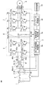
- FIG. 1 is a configuration diagram illustrating a power conversion device according to Embodiment 1 of the present application.
- the power conversion apparatus includes a DC power source 1, a switch 2 (a concept including a relay and a semiconductor switching element), a first smoothing capacitor 3, a first voltage sensor 20, and a differential coupling reactor 4. , A DC / DC converter 5, a second smoothing capacitor 6, a second voltage sensor 30, an inverter 7, an electric motor 8, a control unit 9, and an auxiliary power source 10.
- the DC power supply 1 is chargeable / dischargeable, and exchanges electric power with the motor 8 via the inverter 7.
- the DC / DC converter 5 is provided between the DC power supply 1 and the inverter 7 and boosts the DC voltage supplied from the DC power supply 1.
- the first smoothing capacitor 3 is connected between the DC power supply 1 and the DC / DC converter 5 and smoothes the voltage between the DC power supply 1 and the DC / DC converter 5.
- the first voltage sensor 20 measures the voltage between the high voltage node and the low voltage node of the first smoothing capacitor 3.
- the current sensor 40a measures the current input from the differential coupling reactor 4, and the current sensors 40b and 40c measure the current output between the differential coupling reactor 4 and the DC / DC converter 5. measure.
- the inverter 7 converts the high-voltage DC voltage output from the DC / DC converter 5 into an AC voltage by DC / AC conversion.
- the second smoothing capacitor 6 is connected between the DC / DC converter 5 and the inverter 7, and smoothes the voltage between the DC / DC converter 5 and the inverter 7.
- the second voltage sensor 30 measures the voltage between the high voltage node and the low voltage node of the second smoothing capacitor 6.
- the motor 8 controls the driving force and braking force of the vehicle by applying the AC voltage output from the inverter 7.
- the switch 2 connects the DC power source 1 with the first smoothing capacitor 3 and the DC / DC converter 5 in a closed state, and when the use of the vehicle is finished and stoppage of power is detected.
- an acceleration sensor not shown
- the DC power source 1 and the DC / DC converter 5 via the first smoothing capacitor 3 and the differential coupling reactor 4 are opened. Disconnect.
- the control unit 9 includes a DC / DC converter control unit 9a, an inverter control unit 9b, and a discharge determination instruction unit 9c.
- the discharge determination instructing unit 9c controls the DC / DC converter control unit 9a and the inverter when the collision of the vehicle is detected by, for example, an acceleration sensor (not shown) or when the use of the vehicle is terminated and the power is stopped.
- the unit 9b is instructed to discharge the charge stored in the first smoothing capacitor 3 and the second smoothing capacitor 6.
- the DC / DC converter control unit 9 a controls the switching operation of the semiconductor switching elements 51 a to 51 d that are components of the power semiconductor elements included in the DC / DC converter 5, so that the DC in the DC / DC converter 5 / DC conversion is performed.
- the inverter control unit 9b controls the switching operation of the semiconductor switching elements 71a to 71f in the high-voltage-side power semiconductor element and the low-voltage-side power semiconductor element of the switching arm included in the inverter 7, and the DC / AC in the inverter 7 is controlled. Perform conversion.
- the power semiconductor element is referred to as an arm in which the semiconductor switching elements 51 a to 51 d and the semiconductor rectifier elements 52 a to 52 d are connected in antiparallel to each other, and the arms are connected in series. The thing is called a leg.
- the power semiconductor element is referred to as an arm in which the semiconductor switching elements 71a to 71f and the semiconductor rectifier elements 72a to 72f are connected in antiparallel to each other, and the arms are connected in series. Is called a leg.
- the DC / DC converter 5 is a full bridge type having four semiconductor switching elements 51a to 51d, and two legs (first leg and second leg) formed by connecting upper and lower arms in series are connected in parallel. Configured.
- an IGBT Insulated Gate Bipolar Transistor
- MOSFET Metal-Oxide-Semiconductor-Field-Effect-Transistor
- the inverter 7 is provided with the number of legs corresponding to the number of phases of the motor to be driven. As shown in FIG. 1, when the motor 8 is a three-phase motor, the inverter 7 includes the U phase, the V phase, It consists of three legs of W phase.
- the inverter control unit 9b controls the inverter 7 and adjusts the potentials of the connection nodes Uac, Vac, Wac with the electric motor 8 to control the amount of current flowing through the electric motor 8. As a result, the electric motor 8 controls the driving force and braking force of the vehicle. Moreover, the inverter control part 9b acquires the rotation information of the electric motor 8 together.
- the coupling reactor is formed by winding a first winding 4e and a second winding 4f around a core 4g made of two upper and lower U-shaped iron cores and magnetically coupling each other.
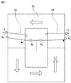
- the differential coupling reactor 4 of the present embodiment is, as shown in FIG. 2, when a direct current is passed through the first winding 4e and the second winding 4f, the core is formed by both windings 4e and 4f. This refers to winding the first winding 4e and the second winding 4f so that the directions of the DC magnetic flux generated in 4g are generated in directions that cancel each other.
- one end sides 4a and 4c of both windings 4e and 4f constituting the differential type coupling reactor 4 are both connected to the positive electrode side of the DC power source 1, and the other end side 4b of the first winding 4e is
- the upper and lower arms having two semiconductor switching elements 51c and 51d are connected to a connection point 50e (first leg) of the upper and lower arms having the two semiconductor switching elements 51a and 51b. Are connected to the connection point 50f (second leg).
- the first winding is operated by performing a complementary operation so that the upper and lower arms of the DC / DC converter 5 connected to the differential coupling reactor 4 are alternately turned on and off, and by shifting the phase of each leg. 4e and the second winding 4f are alternately energized, as shown by the white arrows in FIG. 2, the core 4g generated by the current flowing in the same direction in the first winding 4e and the second winding 4f is not circulated. As indicated by the thick magnetic arrows in FIG. 3 and FIG. 4, two magnetic flux components that change direction depending on the switching state and circulate in the core 4 g are generated simultaneously. In this case, since the magnetic flux and the current are in a proportional relationship, current ripples corresponding to changes in the two magnetic flux components are generated in the first winding 4e and the second winding 4f, respectively.
- the slope of the current ripple generated in the differential coupling reactor 4 is expressed by a mathematical expression.
- the voltage across the first winding 4e is V1e
- the current flowing through the first winding 4e is i1
- the current component due to the circulating magnetic flux constituting this current i1 is i1ac
- the current component due to the non-circulating magnetic flux is i1dc.
- the voltage across the second winding 4f is represented as V2e
- the current flowing through the second winding 4f is represented as i2
- the current component due to the circulating magnetic flux constituting this current i2 is represented as i2ac
- the current component due to the non-circulating magnetic flux is represented as i2dc.
- the current i1 and the current i2 have the same component.
- the current obtained by adding the current i1 and the current i2 is expressed by the following (Equation 5), the current component (i1ac) that circulates is canceled, and the current component (i1dc) generated by the magnetic flux component that does not circulate in each winding.
- the slope is twice that of.
- the input voltage of the differential coupling reactor 4 is Vin
- the output voltage of the DC / DC converter 5 is Vout
- the coupling changes depending on the switching state of the semiconductor switching elements 51b and 51d in the lower arm of the DC / DC converter 5.
- the voltage across the reactor 4 is shown in Table 1.
- FIG. 5 shows a case where D (duty ratio) ⁇ 0.5
- FIG. 6 shows a case where D (duty ratio)> 0.5. 5 and 6, the current components included in the current ripples of the first winding 4e and the second winding 4f are shown when idc ⁇ iac.
- the duty ratio D represents the ratio of the on time to the period T.
- a state (T1), a state (T2), a state (T3), and a state (T4) are sequentially set according to the operation state of the semiconductor switching elements 51b and 51d which are lower arms of the DC / DC converter 5. It becomes a repetitive movement.
- the semiconductor switching elements 51a and 51c are MOSFETs or the like, they operate complementary to the semiconductor switching elements 51b and 51d for synchronous rectification.
- the differential coupling reactor 4 in which the first winding 4e and the second winding 4f are magnetically coupled is formed, the first winding 4e circulates as shown in FIG. A current ripple i1ac generated by the magnetic flux and a current ripple i1dc generated by a non-circulating magnetic flux component as shown in FIG. 2 are generated.
- the second winding 4f has a current ripple i2ac generated by a circulating magnetic flux as shown in FIG. 3 (in this case, generated in a direction opposite to i1ac) and a non-circulating magnetic flux component as shown in FIG. The resulting current ripple i2dc occurs.
- the current slope of i1ac is 4, the current slope of i1dc is 6, and the current slope of the first winding 4e is 10.
- the slope of the total current of the first winding 4e and the second winding 4f is 12 as the total slope of i1dc and i2dc because i1ac and i2ac are canceled.
- This period is a period in which the excitation of the first winding 4e and the second winding 4f is reset, i1ac and i2ac do not change, and the i1dc and i2dc components decrease.
- the current slope of i1ac is 0, the current slope of i1dc is ⁇ 6, and the current slope of the first winding 4e is ⁇ 6.
- the slope of the total current of the first winding 4e and the second winding 4f is ⁇ 12 as the total slope of i1dc and i2dc.
- the differential coupling reactor 4 in which the first winding 4e and the second winding 4f are magnetically coupled is formed, the first winding 4e circulates as shown in FIG. A current ripple i1ac generated by the magnetic flux and a current ripple i1dc generated by a non-circulating magnetic flux component as shown in FIG. 2 are generated.
- the second winding 4f has a current ripple i2ac generated by a circulating magnetic flux as shown in FIG. 4 (in this case, generated in a direction opposite to i1ac) and a non-circulating magnetic flux component as shown in FIG. The resulting current ripple i2dc occurs.
- i1ac has a negative slope.
- the current slope of i1ac is ⁇ 4
- the current slope of i1dc is 6
- the current slope of the first winding 4e is 2.
- the slope of the total current of the first winding 4e and the second winding 4f is 12 because the total slope of i1dc and i2dc is canceled by i1ac and i2ac.
- This period is a period in which the excitation of the first winding 4e and the second winding 4f is reset, i1ac and i2ac do not change, and the i1dc and i2dc components decrease.
- the current slope of i1ac is 0, the current slope of i1dc is ⁇ 6, and the current slope of the first winding 4e is ⁇ 6.
- the slope of the total current of the first winding 4e and the second winding 4f is a total slope of -12 of i1dc and i2dc.
- the differential type FIG. 7 shows a current waveform flowing through the winding of the coupling reactor 4, an operation timing of the DC / DC converter 5, and a current waveform flowing through the semiconductor switching elements 51a to 51d constituting the DC / DC converter 5.
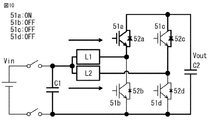
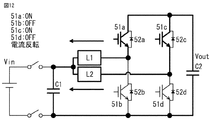
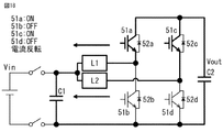
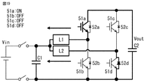
- FIGS. 8 to 19 show the flow locations and operation patterns of the DC / DC converter 5 at this time. 8 to 19, the flow points are indicated by bold lines, and the flow points and the operation pattern of the DC / DC converter 5 are sequentially changed from time to time in each state of FIGS. When the state of FIG. 19 is completed, the state of FIG. 8 is restored.
- the currents i1 and i2 including the frequency component twice the switching frequency when the semiconductor switching element of the DC / DC converter 5 is switched flow through the first winding 4e and the second winding 4f. I understand.
- the power semiconductor included in the DC / DC converter 5 is detected by the DC / DC converter control unit 9a.
- a discharge operation for discharging the charges of the first smoothing capacitor 3 and the second smoothing capacitor 6 by switching the semiconductor switching elements 51a to 51d, which are constituent elements, will be described.
- the switch 2 When the collision of the vehicle is detected or when the use of the vehicle is finished and the stop of the power is detected, the switch 2 is turned off, the inverter control unit 9b of the control unit 9 stops the inverter 7, and the discharge In response to an instruction from the determination instruction unit 9 c, the DC / DC converter control unit 9 a executes the discharging operation of the DC / DC converter 5.
- the control operation for the DC / DC converter 5 in the DC / DC converter control unit 9a is basically the same as that in the normal driving in which the switch 2 is in the ON state. That is, the energy accumulated in the first smoothing capacitor 3 and the second smoothing capacitor 6 is present between the first smoothing capacitor 3 and the second smoothing capacitor 6, the DC / DC converter 5, and the differential coupling reactor. Energy is consumed and discharged by copper loss and iron loss caused by current flowing through 4.
- the switching frequency of the DC / DC converter 5 is made lower than in the normal power conversion operation, and the current ripple is reduced within the allowable current range of the DC / DC converter 5. Make it bigger. This increases the loss, so that the discharge time when the switch 2 is turned off can be shortened.
- FIG. 20 is an explanatory diagram of the switching frequency when the DC / DC converter 5 is switched.
- the auxiliary power source 10 for supplying power to the control unit 9 that drives and controls the DC / DC converter 5 that performs the discharging operation. Therefore, the power conversion device as a whole can be reduced in size.
- FIG. 1 The feature of the power conversion device of the second embodiment of the present application is that the coupling configuration of the coupling reactor 4 used in the first embodiment is a summing type, and the other configurations are the same as those in the first embodiment. Since there is, detailed description of the configuration is omitted.
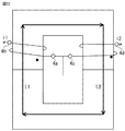
- the summing type coupling reactor 4 is formed by the first winding 4e and the second winding 4f when direct current is passed through the first winding 4e and the second winding 4f.
- FIG. 24 shows the switching timing of the DC / DC converter 5 when the DC / DC converter 5 is subjected to a phase shift operation using the summing type coupling reactor 4, and the current of each part and the coupling reactor 4. It shows the time variation of the winding current.
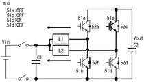
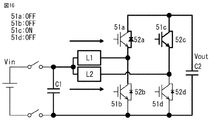
- 25 to 34 show current paths and operation patterns of the DC / DC converter 5. It should be noted that the flow location and operation pattern of the DC / DC converter 5 sequentially change each state of FIGS. 25 to 34 with time change, and return to the state of FIG. 25 when the state of FIG. 34 is completed.
- the DC / DC converter 5 When the phase shift operation is performed on the DC / DC converter 5 using this summing type coupling reactor 4, the DC / DC converter 5 performs a reflux operation as can be seen from FIGS. 24 and 25 to 34.
- a square wave current having a high effective value flows through the first winding 4e and the second winding 4f of the combined coupling reactor 4 to increase the copper loss, and the switch 2 is turned off as in the first embodiment. In this case, the discharge time can be shortened.
Landscapes
- Engineering & Computer Science (AREA)
- Power Engineering (AREA)
- Dc-Dc Converters (AREA)
Abstract
直流電源(1)とインバータ(7)との間に磁気結合した結合リアクトル(4)とDC/DC変換器(5)が設けられ、直流電源(1)と結合リアクトル(4)の間に第1平滑コンデンサ(3)が、DC/DC変換器(5)とインバータ(7)との間に第2平滑コンデンサ(6)が設けられ、かつインバータ(7)とDC/DC変換器(5)のスイッチング動作を制御する制御部(9)を備え、制御部(9)はDC/DC変換器(5)の上下アームを構成する半導体スイッチング素子(51a)と(51b)、(51c)と(51d)が交互にオン/オフするように相補動作させ、かつ左右のレグのスイッチング位相をずらして動作させて結合リアクトル(4)とDC/DC変換器(5)のエネルギ損失により両平滑コンデンサ(3)、(6)の蓄積電荷を放電する。
Description
本願は、例えば電動車両に搭載される電力変換装置に関する。
従来、充放電可能な直流電源と、直流電源から供給される直流電圧を昇圧する昇圧コンバータと、直流電源と昇圧コンバータとの間の電圧を平滑化する第1平滑コンデンサと、昇圧コンバータから出力される高圧の直流電圧を交流電圧に変換するインバータと、昇圧コンバータとインバータとの間の電圧を平滑化する第2平滑コンデンサと、インバータから出力される交流電圧が印加されることにより、車両の駆動力および制動力が制御される三相交流電動機を備えた電動車両が知られている。
このような電動車両では、車両の安全性を確保するために、車両の衝突時、あるいは動力の停止時に、平滑コンデンサに蓄えられた高電圧の電荷を速やかに放電し、感電を防止する必要がある。
また、放電時間を早くするために昇圧コンバータを放電制御するための動作電源となるバックアップ電源の容量を小さくして、電力変換装置を小型化することが必要とされている。
このため、従来は、例えば下記の特許文献1及び2に記載されるような技術が提案されている。
特許文献1に示される電動車両では、2個の双方向DC/DCコンバータを備えているとともに、2個の双方向DC/DCコンバータの低電圧端と高電圧端にコンデンサが接続されている。制御装置は、走行時には、それぞれの双方向DC/DCコンバータの半導体スイッチング素子に対して、オンのタイミングが相互にずれているとともにオフのタイミングが相互にずれている駆動パルス信号を供給している。一方、コンデンサを放電する際は、その放電時間を早める技術として、夫々の双方向DC/DCコンバータの半導体スイッチング素子に対して、オンのタイミングとオフのタイミングがそれぞれ一致している駆動パルス信号を供給することを特徴としている。
また、特許文献2に示される電力変換装置では、従来のインバータの上下アームを交互にオンオフさせて放電する方法では、インバータを構成するアームが短絡している場合、過電流等により放電できないことに対し、4アームを直列にしたDC/DC変換器を用い、アーム短絡の有無を検出し、入出力のコンデンサに蓄積された電荷を結合リアクトルとDC/DC変換器を介して放電させる技術が示されている。
しかしながら、上記の特許文献1、2に記載されたいずれの従来技術の場合も、結合リアクトルに流れる電流がいずれもスイッチング周波数の三角波電流であり、その電流成分にDC/DCコンバータのスイッチング周波数成分しかなく、通流する際の銅損が小さいため、コンデンサのエネルギを消費させる効果が少なく放電に時間を要し、放電時間を早くするためにDC/DCコンバータを放電制御するための動作電源となるバックアップ電源の電源容量が依然として大きいという課題がある。
本願は、上記のような問題点を解消するために成されたものであって、DC/DCコンバータの入力段に磁気結合した一対の結合型の結合リアクトルを設け、DC/DCコンバータの動作に伴ってコンデンサの放電時間を従来よりも早め、放電制御のためにDC/DCコンバータを駆動するためのバックアップ電源を小型化することができる電力変換装置の提供を目的とする。
本願に開示される電力変換装置は、
直流電源と電動機を駆動するインバータとの間に配置された、磁気結合した結合リアクトルおよび電圧変換用のDC/DC変換器と、
上記直流電源と上記結合リアクトルとの間に接続された第1平滑コンデンサと、
上記DC/DC変換器と上記インバータとの間に接続された第2平滑コンデンサと、
上記第1平滑コンデンサと上記直流電源との間に挿入された上記直流電源のオン/オフ用のスイッチと、
上記インバータおよび上記DC/DC変換器に含まれる半導体スイッチング素子のスイッチング動作を制御する制御部とを備え、
上記DC/DC変換器は、上記半導体スイッチング素子を有する上下一対のアームを直列接続してなるレグの2つを並列に接続して構成されるフルブリッジ型のものであり、上記結合リアクトルは、上記結合リアクトルを構成する第1巻線と第2巻線の各一端側が共に上記直流電源の正極側に接続され、上記第1巻線の他端側は上記レグのうちの第1レグを構成する上下アームの接続点に接続され、また、上記第2巻線の他端側は上記レグのうちの第2レグを構成する上下アームの接続点にそれぞれ接続されている電力変換装置であって、
上記制御部は、放電指令に応じて上記スイッチを解放し、上記DC/DC変換器の上下のアームを構成する上記半導体スイッチング素子が交互にオン/オフするように相補動作させ、かつ一対の上記レグのスイッチング位相をずらして動作させるものである。
直流電源と電動機を駆動するインバータとの間に配置された、磁気結合した結合リアクトルおよび電圧変換用のDC/DC変換器と、
上記直流電源と上記結合リアクトルとの間に接続された第1平滑コンデンサと、
上記DC/DC変換器と上記インバータとの間に接続された第2平滑コンデンサと、
上記第1平滑コンデンサと上記直流電源との間に挿入された上記直流電源のオン/オフ用のスイッチと、
上記インバータおよび上記DC/DC変換器に含まれる半導体スイッチング素子のスイッチング動作を制御する制御部とを備え、
上記DC/DC変換器は、上記半導体スイッチング素子を有する上下一対のアームを直列接続してなるレグの2つを並列に接続して構成されるフルブリッジ型のものであり、上記結合リアクトルは、上記結合リアクトルを構成する第1巻線と第2巻線の各一端側が共に上記直流電源の正極側に接続され、上記第1巻線の他端側は上記レグのうちの第1レグを構成する上下アームの接続点に接続され、また、上記第2巻線の他端側は上記レグのうちの第2レグを構成する上下アームの接続点にそれぞれ接続されている電力変換装置であって、
上記制御部は、放電指令に応じて上記スイッチを解放し、上記DC/DC変換器の上下のアームを構成する上記半導体スイッチング素子が交互にオン/オフするように相補動作させ、かつ一対の上記レグのスイッチング位相をずらして動作させるものである。
本願に開示される電力変換装置によれば、第1平滑コンデンサと第2平滑コンデンサとの間にDC/DC変換器と結合リアクトルを介して循環電流を流すことができ、電流が流れる経路で生じる銅損、結合リアクトルのコアで生じる鉄損、DC/DC変換器で生じる損失により、第1平滑コンデンサと第2平滑コンデンサに蓄積された電荷を速やかに放電させることができる。これにより、第1平滑コンデンサ及び第2平滑コンデンサの放電時間を従来よりも早め、放電制御のためにDC/DCコンバータを駆動するためのバックアップ電源を小型化することが可能となる。
また、直流電流を流した場合に生じる直流磁束が互いに打ち消す方向に生じる差動型に結合した結合リアクトルを用いる場合には、通流する電流成分に周波数の2倍の成分を発生させることで銅損を大きくすることができる。また、直流電流を流した場合に生じる直流磁束が互いに強め合う方向に生じる和動型に結合した結合リアクトルを用いる場合には、通流する電流を還流電流により方形波状とすることで電流実効値を大きくして結合リアクトルの銅損を大きくすることができる。
実施の形態1.
図1は、本願の実施の形態1による電力変換装置を示す構成図である。
図1において、本実施の形態の電力変換装置は、直流電源1、スイッチ2(リレー並びに半導体スイッチング素子を含む概念)、第1平滑コンデンサ3、第1電圧センサ20、差動型の結合リアクトル4、DC/DC変換器5、第2平滑コンデンサ6、第2電圧センサ30、インバータ7、電動機8、制御部9、補助電源10を備えている。
図1は、本願の実施の形態1による電力変換装置を示す構成図である。
図1において、本実施の形態の電力変換装置は、直流電源1、スイッチ2(リレー並びに半導体スイッチング素子を含む概念)、第1平滑コンデンサ3、第1電圧センサ20、差動型の結合リアクトル4、DC/DC変換器5、第2平滑コンデンサ6、第2電圧センサ30、インバータ7、電動機8、制御部9、補助電源10を備えている。
直流電源1は、充放電可能であり、インバータ7を介して電動機8と電力をやり取りする。DC/DC変換器5は、直流電源1とインバータ7との間に設けられ、直流電源1から供給される直流電圧を昇圧する。第1平滑コンデンサ3は、直流電源1とDC/DC変換器5との間に接続され、直流電源1とDC/DC変換器5との間の電圧を平滑化する。第1電圧センサ20は、第1平滑コンデンサ3の高電圧ノードと低電圧ノードとの間の電圧を計測する。電流センサ40aは差動型の結合リアクトル4から入力される電流を計測し、また、電流センサ40b、40cは差動型の結合リアクトル4とDC/DC変換器5の間に出力される電流を計測する。
インバータ7は、DC/DC変換器5から出力される高圧の直流電圧を、DC/AC変換により交流電圧に変換する。第2平滑コンデンサ6は、DC/DC変換器5とインバータ7との間に接続され、DC/DC変換器5とインバータ7との間の電圧を平滑化する。第2電圧センサ30は、第2平滑コンデンサ6の高電圧ノードと低電圧ノードとの間の電圧を計測する。
電動機8は、インバータ7から出力される交流電圧が印加されることにより、車両の駆動力および制動力が制御される。スイッチ2は、車両の駆動時には、直流電源1と第1平滑コンデンサ3およびDC/DC変換器5とを閉状態で接続し、また、車両の使用が終了して動力の停止が検知された場合、あるいは図示しない加速度センサなどにより車両の衝突が検知された場合には、直流電源1と第1平滑コンデンサ3および差動型の結合リアクトル4を介したDC/DC変換器5とを開状態で切断する。
制御部9は、DC/DC変換器制御部9a、インバータ制御部9b、および放電判定指示部9cを有している。放電判定指示部9cは、例えば図示しない加速度センサにより、車両の衝突を検知した場合、あるいは、車両の使用を終了し動力を停止状態とする場合に、DC/DC変換器制御部9aおよびインバータ制御部9bに対して、第1平滑コンデンサ3、第2平滑コンデンサ6に蓄えられた電荷を放電するように指示を出す。
DC/DC変換器制御部9aは、DC/DC変換器5に含まれるパワー半導体素子の構成要素である半導体スイッチング素子51a~51dのスイッチング動作を制御して、DC/DC変換器5でのDC/DC変換を行う。インバータ制御部9bは、インバータ7に含まれるスイッチングアームの高電圧側パワー半導体素子および低電圧側パワー半導体素子内の半導体スイッチング素子71a~71fのスイッチング動作を制御して、インバータ7でのDC/AC変換を行う。
DC/DC変換器5において、パワー半導体素子は、半導体スイッチング素子51a~51dと半導体整流素子52a~52dとを相互に逆並列に接続したものを単位としてアームと称し、またそのアームを直列接続したものをレグと称する。同様に、インバータ7において、パワー半導体素子は、半導体スイッチング素子71a~71fと半導体整流素子72a~72fとを相互に逆並列に接続したものを単位としてアームと称し、またそのアームを直列接続したものをレグと称する。
ここで、DC/DC変換器5の構成について詳細に説明する。
DC/DC変換器5は、4つの半導体スイッチング素子51a~51dを有するフルブリッジ型であり、上下のアームを直列接続してなるレグの2つ(第1レグと第2レグ)を並列に接続して構成されている。なお、図1では半導体スイッチング素子にIGBT(Insulated Gate Bipolar Transistor)を用いて記載しているがMOSFET(Metal-Oxide-Semiconductor-Field-Effect-Transistor)等を使用してもよい。
DC/DC変換器5は、4つの半導体スイッチング素子51a~51dを有するフルブリッジ型であり、上下のアームを直列接続してなるレグの2つ(第1レグと第2レグ)を並列に接続して構成されている。なお、図1では半導体スイッチング素子にIGBT(Insulated Gate Bipolar Transistor)を用いて記載しているがMOSFET(Metal-Oxide-Semiconductor-Field-Effect-Transistor)等を使用してもよい。
続いて、インバータ7の詳細な構成について説明する。
インバータ7は、駆動する電動機の相数に対応するレグ数が設けられており、図1に示されるように、電動機8が三相の電動機である場合、インバータ7は、U相、V相、W相の3つのレグで構成される。
インバータ7は、駆動する電動機の相数に対応するレグ数が設けられており、図1に示されるように、電動機8が三相の電動機である場合、インバータ7は、U相、V相、W相の3つのレグで構成される。
インバータ制御部9bは、インバータ7を制御して、電動機8との接続ノードUac、Vac、Wacの電位を調整することで、電動機8に流れる電流量を制御する。この結果、電動機8が車両の駆動力および制動力を制御することとなる。また、インバータ制御部9bは、電動機8の回転情報を併せて取得する。
次に、図2~図4を用いて結合リアクトル4の構成について説明する。
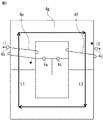
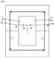
ここに、結合リアクトルは、上下2つのU字型の鉄心からなるコア4gに第1巻線4eと第2巻線4fを巻いて互いに磁気結合させたものである。特に、本実施の形態の差動型の結合リアクトル4とは、図2に示すように、第1巻線4eと第2巻線4fに直流を流した場合、両巻線4e、4fによりコア4gに生じる直流磁束の向きが互いに打ち消し合う方向に生じるように、第1巻線4eと第2巻線4fを巻線することをいう。
ここに、結合リアクトルは、上下2つのU字型の鉄心からなるコア4gに第1巻線4eと第2巻線4fを巻いて互いに磁気結合させたものである。特に、本実施の形態の差動型の結合リアクトル4とは、図2に示すように、第1巻線4eと第2巻線4fに直流を流した場合、両巻線4e、4fによりコア4gに生じる直流磁束の向きが互いに打ち消し合う方向に生じるように、第1巻線4eと第2巻線4fを巻線することをいう。
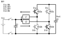
そして、この差動型の結合リアクトル4を構成する両巻線4e、4fの一端側4a、4cは共に直流電源1の正極側に接続され、また、第1巻線4eの他端側4bは2つの半導体スイッチング素子51a、51bを有する上下アームの接続点50e(第1レグ)に接続され、また、第2巻線4fの他端側4dは2つの半導体スイッチング素子51c、51dを有する上下アームの接続点50f(第2レグ)に接続されている。
この差動型の結合リアクトル4に接続された、DC/DC変換器5の上下アームが交互にオン/オフするように相補動作させるとともに、各レグの位相をずらして動作させて第1巻線4e、第2巻線4fを交互に励磁すると、図2の白抜き矢印で示すように、第1巻線4eと第2巻線4fに同方向に電流が流れることにより生じるコア4gを循環しない磁束成分、および図3及び図4の太い矢印で示すように、スイッチング状態によって向きを変えてコア4g内を循環する磁束成分の2つの磁束成分が同時に生じる。この場合、磁束と電流とは比例関係にあるため、この2つの磁束成分の変化に対応した電流リプルが第1巻線4eと第2巻線4fにそれぞれ生じることになる。
ここで、差動型の結合リアクトル4に生じる電流リプルの傾きを数式にて示す。第1巻線4eの両端電圧をV1e、第1巻線4eに流れる電流をi1、この電流i1を構成する循環磁束による電流成分をi1ac、循環しない磁束による電流成分をi1dcとする。また、第2巻線4fの両端電圧をV2e、第2巻線4fに流れる電流をi2、この電流i2を構成する循環磁束による電流成分をi2ac、循環しない磁束による電流成分をi2dcとして表わし、ここでは簡単のため、電流i1と電流i2のそれぞれの成分の大きさは等しいものとする。
第1巻線4eおよび第2巻線4fが生じさせる自己インダクタンスをL、相互インダクタンスをMとすると、第1巻線4e、第2巻線4fに生じる電圧V1e、V2eはファラデーの法則を用いて(式1)(式2)で表わされる。


電流i1および電流i2は、循環磁束による電流成分i1ac、循環しない磁束による電流成分i1dcから構成されているため、(式3)(式4)で表わされる。


また電流i1と電流i2を合計した電流は、次の(式5)で表わされるように、循環する電流成分(i1ac)は打ち消されて、各巻線の循環しない磁束成分で生じる電流成分(i1dc)の2倍の傾きとなる。

(式1)~(式4)より電流i1、電流i2を構成する電流成分i1ac、i1dcを求めると(式6)(式7)で表わすことができる。


差動型の結合リアクトル4の入力電圧をVin、DC/DC変換器5の出力電圧をVoutとし、DC/DC変換器5の下アームの半導体スイッチング素子51b、51dのスイッチング状態によって、変化する結合リアクトル4の両端電圧を表1に記す。
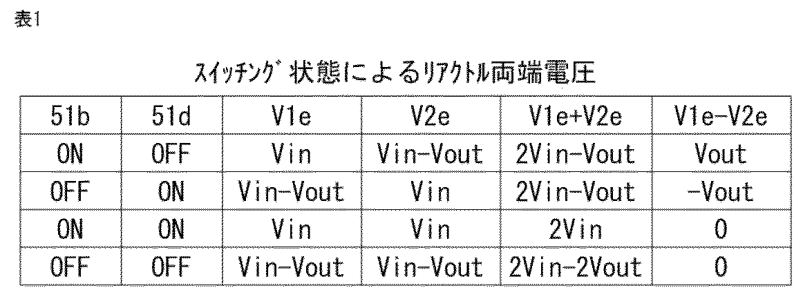
この電圧を(式6)(式7)に代入すると、スイッチング状態に応じて変化する電流の傾きを求めることができる。
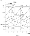
次に、車両の通常駆動時、すなわちスイッチ2がオンされた状態において、DC/DC変換器5の2組の各レグを、位相をずらして交互に動作させて第1巻線4e、第2巻線4fを交互に励磁する通常の電力変換動作時の場合に、上記(式3)~(式7)で求めた電流の傾きから、第1巻線4e、第2巻線4fに生じる電流リプルについて図5および図6を用いて説明する。
図5は、D(デューティ比)<0.5の場合であり、図6は、D(デューティ比)>0.5の場合である。
また、図5及び図6において、第1巻線4e及び第2巻線4fの電流リプルに含まれる電流成分がidc<iacの時のものを示す。デューティ比Dは、周期Tに対するオン時間の比率を表す。
また、図5及び図6において、第1巻線4e及び第2巻線4fの電流リプルに含まれる電流成分がidc<iacの時のものを示す。デューティ比Dは、周期Tに対するオン時間の比率を表す。
動作モードとしては、DC/DC変換器5の下アームである半導体スイッチング素子51b、51dの動作状態により状態(T1)、状態(T2)、状態(T3)、状態(T4)の4モードを順次繰り返す動きとなる。なお、半導体スイッチング素子51a、51cはMOSFET等であれば同期整流用としてそれぞれ半導体スイッチング素子51b、51dと相補的に動作する。
[A]まず、図5に示すように、D<0.5の場合に第1巻線4e及び第2巻線4fに生じる電流リプルについて説明する。
(1)状態(T1)の期間は、半導体スイッチング素子51bがオン、半導体スイッチング素子51dがオフであり、直流電源1から第1巻線4eを通って直流電源1に戻る電流i1の電流ループと、第2巻線4f、半導体整流素子52cを通り、第2平滑コンデンサ6を経て直流電源1に戻る電流i2との2つの電流ループが形成される。
この時、第1巻線4eと第2巻線4fが磁気的に結合した差動型の結合リアクトル4を形成しているため、第1巻線4eには、図4に示すような循環する磁束により生じる電流リプルi1acと、図2に示すような循環しない磁束成分により生じる電流リプルi1dcとが生じる。
第2巻線4fには、図3に示すような循環する磁束により生じる電流リプルi2ac(この場合、i1acとは逆向きとなる方向で生じる)と、図2に示すような循環しない磁束成分により生じる電流リプルi2dcとが生じる。
ここで説明を簡単にするため、仮に、循環磁束により生じる電流成分の傾きを4、循環しない磁束により生じる電流成分の傾きを6とし、DC/DC変換器5のスイッチング状態により変化する、第1巻線4e、第2巻線4fに生じる電流リプル波形の変化をこの数値例を用いて説明する。
この期間ではi1acの電流傾き4、i1dcの電流傾き6となり、第1巻線4eの電流傾きは10となる。また、第1巻線4eと第2巻線4fの合計電流の傾きは、i1acとi2acがキャンセルされ、i1dcとi2dcの合計傾きで12となる。
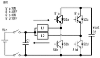
(2)状態(T2)の期間は、半導体スイッチング素子51bがオフ、半導体スイッチング素子51dがオフであり、直流電源1から第1巻線4e、半導体整流素子52a、第2平滑コンデンサ6を経て直流電源1へ戻る電流i1の電流ループと、直流電源1から第2巻線4f、半導体整流素子52c、第2平滑コンデンサ6を経て直流電源1へ戻る電流i2の電流ループが形成される。
この期間は、第1巻線4eと第2巻線4fの励磁がリセットされる期間であり、i1ac、i2acは変化せず、i1dc、i2dc成分が減少する。i1acの電流傾きが0、i1dcの電流の傾きが-6となり、第1巻線4eの電流傾きは-6となる。第1巻線4eと第2巻線4fの合計電流の傾きは、i1dcとi2dcの合計傾きで-12となる。
(3)状態(T3)の期間は、半導体スイッチング素子51bがオフ、半導体スイッチング素子51dがオンであり、直流電源1から第1巻線4e、半導体整流素子52a、第2平滑コンデンサ6を経て直流電源1へ戻る電流i1の電流ループと、直流電源1から第2巻線4f、半導体スイッチング素子51dを経て直流電源1に戻る電流i2の電流ループが形成される。
この時、第1巻線4eと第2巻線4fが磁気的に結合した差動型の結合リアクトル4を形成しているため、第1巻線4eには、図3に示すような循環する磁束により生じる電流リプルi1acと、図2に示すような循環しない磁束成分により生じる電流リプルi1dcとが生じる。
第2巻線4fには、図4に示すような循環する磁束により生じる電流リプルi2ac(この場合、i1acとは逆向きとなる方向で生じる)と、図2に示すような循環しない磁束成分により生じる電流リプルi2dcとが生じる。
この時、第2巻線4fからの磁束が、第1巻線4eの磁束を減じる方向に磁気結合するため、i1acはマイナスの傾きとなる。同様に、i1acの電流傾きが-4、i1dcの電流の傾きが6となり、第1巻線4eの電流傾きは2となる。第1巻線4eと第2巻線4fの合計電流の傾きは、i1acとi2acがキャンセルされ、i1dcとi2dcの合計傾きで12となる。
(4)状態(T4)の期間は、状態(T2)の場合と同様、半導体スイッチング素子51bがオフ、半導体スイッチング素子51dがオフであり、直流電源1から第1巻線4e、半導体整流素子52a、第2平滑コンデンサ6を経て直流電源1へ戻る電流i1の電流ループと、直流電源1から第2巻線4f、半導体整流素子52c、第2平滑コンデンサ6を経て直流電源1へ戻る電流i2の電流ループが形成される。
この期間は、第1巻線4eと第2巻線4fの励磁がリセットされる期間であり、i1ac、i2acは変化せず、i1dc、i2dc成分が減少する。i1acの電流傾きが0、i1dcの電流の傾きが-6となり、第1巻線4eの電流傾きは-6となる。第1巻線4eと第2巻線4fの合計電流の傾きは、i1dcとi2dcの合計の傾き-12となる。
以上説明したように、D<0.5の場合、第1巻線4eの場合、状態(T3)の期間で電流i1の傾きがプラスとなり、電流成分として、DC/DC変換器5をスイッチするスイッチング周波数の2倍の電流成分が含まれることになる。
[B]次に、図6に示すように、D>0.5の場合に第1巻線4e及び第2巻線4fに生じる電流リプルについて説明する。
(1)状態(T1)の期間は、半導体スイッチング素子51bがオン、半導体スイッチング素子51dがオンであり、直流電源1から第1巻線4eを通って直流電源1に戻る電流i1の電流ループと、第2巻線4fを通って直流電源1に戻る電流i2の電流ループが形成される。
この期間、第1巻線4eと第2巻線4fには循環する磁束成分による電流i1ac、i2acはゼロとなり、循環しない磁束成分により生じる電流リプルi1dc、i2dcが増加する。
したがって、この期間では、上記のD<0.5の場合と同様に、説明を簡単にするため仮に、i1acの電流傾きを0、i1dcの電流傾きを6とすると、第1巻線4eの電流傾きは6となる。第1巻線4eと第2巻線4fの合計電流の傾きは、i1acとi2ac成分が無いため、i1dcとi2dcの合計傾きで12となる。
(2)状態(T2)の期間は、半導体スイッチング素子51bがオン、半導体スイッチング素子51dがオフであり、直流電源1から第1巻線4eを通って直流電源1に戻る電流i1の電流ループと、第2巻線4f、半導体整流素子52c、第2平滑コンデンサ6を経て直流電源1に戻る電流i2の電流ループが形成される。
この期間、第1巻線4eと第2巻線4fには循環する磁束が生じ、i1acが増加、i2acは減少し、循環しない成分により生じるi1dc、i2dcは減少する。したがって、i1acの電流傾きを4、i1dcの電流傾きを-6とすると、第1巻線4eの電流傾きは-2となる。第1巻線4eと第2巻線4fの合計電流の傾きは、i1acとi2ac成分がキャンセルされ、i1dcとi2dcの合計傾きで-12となる。
(3)状態(T3)の期間は、半導体スイッチング素子51bがオン、半導体スイッチング素子51dがオンであり、状態(T1)と同様である。
(4)状態(T4)の期間は、半導体スイッチング素子51bがオフ、半導体スイッチング素子51dがオンであり、直流電源1から第1巻線4e、半導体整流素子52a、第2平滑コンデンサ6を経て直流電源1に戻る電流i1の電流ループと、第2巻線4fを通って直流電源1に戻る電流i2の電流ループが形成される。
この期間、第1巻線4eと第2巻線4fには循環する磁束が生じ、i1acが減少、i2acは増加し、循環しない成分により生じるi1dc、i2dcは減少する。したがって、i1acの電流傾き-4、i1dcの電流傾き-6となり、第1巻線4eの電流傾きは-10となる。第1巻線4eと第2巻線4fの合計電流の傾きは、i1acとi2ac成分がキャンセルされ、i1dcとi2dcの合計傾きで-12となる。
以上説明したように、D>0.5の時、第1巻線4eであれば状態(T2)の期間で電流i1の傾きがマイナスとなるため、電流成分として、DC/DC変換器5をスイッチするスイッチング周波数の2倍の電流成分が含まれることになる。
電流成分に、DC/DC変換器5をスイッチングするスイッチング周波数の2倍の電流成分を多く含ませるためには、D<0.5の時には、状態(T3)の期間において次の(式8)を、またD>0.5の時には、状態(T2)の期間において次の(式9)を、それぞれ満たす必要がある。
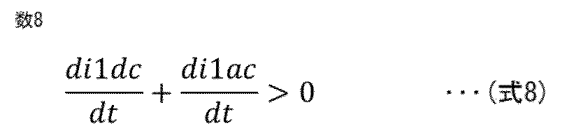
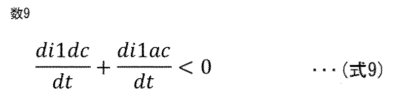
(式6)(式7)と表1を用いて(式8)(式9)の関係式をL(自己インダクタンス)、M(相互インダクタンス)、D(デューティ比)を用いて整理すると、次の(式10)(式11)で表わされる。
D<0.5の場合、

D>0.5の場合、
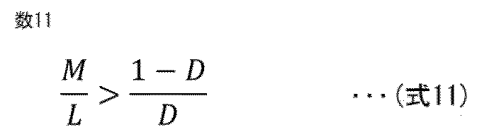
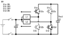
上記関係式を満たす条件において、DC/DC変換器5を用い、下アームをD>0.5の条件で第1平滑コンデンサ3と第2平滑コンデンサ6を放電動作させた場合、差動型の結合リアクトル4の巻線に流れる電流波形、DC/DC変換器5の動作タイミング、および、DC/DC変換器5を構成する半導体スイッチング素子51a~51dに流れる電流波形を図7に示す。また、この時のDC/DC変換器5の通流箇所と動作パターンを図8~図19に示す。なお、図8~図19において、通流箇所は太線で示しており、DC/DC変換器5の通流箇所と動作パターンは、時間変化とともに図8~図19の各状態を順次変遷して行き、図19の状態が終われば図8の状態に戻る。
以上より、第1巻線4e及び第2巻線4fには、DC/DC変換器5の半導体スイッチング素子をスイッチングする場合のスイッチング周波数の2倍の周波数成分を含む電流i1、i2が流れることが分かる。
次に、車両の衝突を検知した場合、あるいは車両の使用が終了して動力の停止が検知された場合において、DC/DC変換器制御部9aにより、DC/DC変換器5に含まれるパワー半導体素子の構成要素である半導体スイッチング素子51a~51dをスイッチング動作させ、第1平滑コンデンサ3、第2平滑コンデンサ6の電荷を放電する放電動作について説明する。
車両の衝突を検知した場合、あるいは車両の使用が終了して動力の停止が検知された場合、スイッチ2がオフされるとともに、制御部9のインバータ制御部9bによりインバータ7を停止し、かつ放電判定指示部9cからの指示により、DC/DC変換器制御部9aはDC/DC変換器5の放電動作を実行する。
この場合のDC/DC変換器制御部9aにおけるDC/DC変換器5に対する制御動作は、上述したスイッチ2がオン状態にある通常駆動時の場合と基本的に同じである。すなわち、第1平滑コンデンサ3および第2平滑コンデンサ6に蓄積されたエネルギは、第1平滑コンデンサ3と第2平滑コンデンサ6の間に存在する、DC/DC変換器5、差動型の結合リアクトル4を経由して電流が流れることにより生じる銅損および鉄損によりエネルギ消費され放電される。
ただし、この場合の放電動作時は、通常の電力変換動作時と比べて、DC/DC変換器5のスイッチング周波数を低くし、DC/DC変換器5が許容される電流範囲内において電流リプルを大きくなるようにする。このようにすると、損失が増加するので、スイッチ2がオフした場合の放電時間を早くすることができる。
このような放電動作をする場合、第1平滑コンデンサ3、第2平滑コンデンサ6と差動型の結合リアクトル4においてLC共振が生じるため、DC/DC変換器5のスイッチング周波数を下げ過ぎると、DC/DC変換器5、第1平滑コンデンサ3、および、第2平滑コンデンサ6の許容値を超える共振電圧、共振電流が生じる可能性がある。
そこで、図20に示すように、第1平滑コンデンサ3、第2平滑コンデンサ6の放電開始時から放電が進むにつれてDC/DC変換器5のスイッチング周波数が、通常の電力変換動作時の周波数から次第に低くなるような制御を行うと、構成する部品の保護と放電時間の短縮の両立が可能となる。図20は、DC/DC変換器5をスイッチング動作する場合のスイッチング周波数についての説明図である。
このようにして第1平滑コンデンサ3、第2平滑コンデンサ6の放電時間が早くなると、放電動作を行うDC/DC変換器5を駆動制御する制御部9に対して電力供給するための補助電源10の電源容量を小さくすることができ、電力変換装置全体の小型化が図れる。
実施の形態2.
本願の実施の形態2の電力変換装置の特徴は、実施の形態1に用いた結合リアクトル4の結合構成を和動型にしたものであり、その他の構成は実施の形態1の場合と同じであるので、詳しい構成の説明は省略する。
本願の実施の形態2の電力変換装置の特徴は、実施の形態1に用いた結合リアクトル4の結合構成を和動型にしたものであり、その他の構成は実施の形態1の場合と同じであるので、詳しい構成の説明は省略する。
ここに、和動型の結合リアクトル4とは、図21に示すように、第1巻線4eと第2巻線4fに直流を流した場合、第1巻線4e及び第2巻線4fによりコア4gに生じる直流磁束の向きが互いに強め合う方向に生じるように、第1巻線4eと第2巻線4fを巻線することをいう。
図24は、この和動型の結合リアクトル4を用いて、DC/DC変換器5を位相シフト動作させた場合の、DC/DC変換器5のスイッチングタイミング、および各部の電流と結合リアクトル4の巻線電流の時間変化を示したものである。また、図25~図34には、DC/DC変換器5の電流経路と動作パターンを示す。なお、DC/DC変換器5の通流箇所と動作パターンは、時間変化とともに図25~図34の各状態を順次変遷して行き、図34の状態が終われば図25の状態に戻る。
この和動型の結合リアクトル4を用いて、DC/DC変換器5を位相シフト動作させると、図24、図25~図34から分かるように、DC/DC変換器5が還流動作となるため、和動型の結合リアクトル4の第1巻線4e、第2巻線4fに実効値の高い方形波状の電流が流れて銅損が増え、実施の形態1の場合と同様にスイッチ2がオフした場合の放電時間を早くすることができる。
以上、本願の開示は、様々な例示的な実施の形態及び実施例が記載されているが、1つ、または複数の実施の形態に記載された様々な特徴、態様、及び機能は特定の実施の形態の適用に限られるのではなく、単独で、または様々な組み合わせで実施の形態に適用可能である。
従って、例示されていない無数の変形例が、本願明細書に開示される技術の範囲内において想定される。例えば、少なくとも1つの構成要素を変形する場合、追加する場合または省略する場合、さらには、少なくとも1つの構成要素を抽出し、他の実施の形態の構成要素と組み合わせる場合が含まれるものとする。
従って、例示されていない無数の変形例が、本願明細書に開示される技術の範囲内において想定される。例えば、少なくとも1つの構成要素を変形する場合、追加する場合または省略する場合、さらには、少なくとも1つの構成要素を抽出し、他の実施の形態の構成要素と組み合わせる場合が含まれるものとする。
1 直流電源、2 スイッチ、3 第1平滑コンデンサ、4 結合リアクトル、4e 第1巻線、4f 第2巻線、4g コア、40a,40b,40c 電流センサ、5 DC/DC変換器、51a~51d 半導体スイッチング素子、6 第2平滑コンデンサ、7 インバータ、71a~71f 半導体スイッチング素子、8 電動機、9 制御部、9a DC/DC変換器制御部、9b インバータ制御部、9c 放電判定指示部、10 補助電源、20 第1電圧センサ、30 第2電圧センサ。
Claims (10)
- 直流電源と電動機を駆動するインバータとの間に配置された、磁気結合した結合リアクトルおよび電圧変換用のDC/DC変換器と、
上記直流電源と上記結合リアクトルとの間に接続された第1平滑コンデンサと、
上記DC/DC変換器と上記インバータとの間に接続された第2平滑コンデンサと、
上記第1平滑コンデンサと上記直流電源との間に挿入された上記直流電源のオン/オフ用のスイッチと、
上記インバータおよび上記DC/DC変換器に含まれる半導体スイッチング素子のスイッチング動作を制御する制御部とを備え、
上記DC/DC変換器は、上記半導体スイッチング素子を有する上下一対のアームを直列接続してなるレグの2つを並列に接続して構成されるフルブリッジ型のものであり、上記結合リアクトルは、上記結合リアクトルを構成する第1巻線と第2巻線の各一端側が共に上記直流電源の正極側に接続され、上記第1巻線の他端側は上記レグのうちの第1レグを構成する上下アームの接続点に接続され、また、上記第2巻線の他端側は上記レグのうちの第2レグを構成する上下アームの接続点にそれぞれ接続されている電力変換装置であって、
上記制御部は、放電指令に応じて上記スイッチを解放し、上記DC/DC変換器の上下のアームを構成する上記半導体スイッチング素子が交互にオン/オフするように相補動作させ、かつ一対の上記レグのスイッチング位相をずらして動作させる電力変換装置。 - 上記制御部は、上記第1平滑コンデンサと上記第2平滑コンデンサとの間に上記結合リアクトルと上記DC/DC変換器を介して交流電流を循環させて、上記結合リアクトルおよび上記DC/DC変換器によるエネルギ損失により上記第1平滑コンデンサおよび上記第2平滑コンデンサに蓄積された電荷を放電させるように上記DC/DC変換器を制御する請求項1に記載の電力変換装置。
- 上記結合リアクトルは、上記第1巻線と上記第2巻線に直流を流した場合、上記第1巻線及び上記第2巻線により生じる直流磁束の向きが互いに打ち消し合う方向に生じる差動型のものである請求項1又は請求項2に記載の電力変換装置。
- 上記DC/DC変換器の上記半導体スイッチング素子をオン/オフするデューティ比をD、上記結合リアクトルの自己インダクタンスをL、相互インダクタンスをMとすると、
D<0.5の場合には、M/L>D/(1-D)
D>0.5の場合には、M/L>(1-D)/D
の各々の関係を満たすように設定することにより、上記結合リアクトルに上記DC/DC変換器のスイッチング周波数の2倍の成分を含む交流電流を流す請求項3に記載の電力変換装置。 - 上記制御部は、上記スイッチがオフした場合、上記第1平滑コンデンサと上記第2平滑コンデンサの電圧もしくは電圧差に応じて上記DC/DC変換器の上記半導体スイッチング素子をオン/オフするデューティ比を可変し、予め設定した一定の許容値を超えない範囲で上記結合リアクトルに流れるリプル電流を最大化させる請求項4に記載の電力変換装置。
- 上記結合リアクトルは、上記第1巻線と上記第2巻線に直流を流した場合、上記第1巻線及び上記第2巻線により生じる直流磁束の向きが互いに強め合う方向に生じる和動型のものである請求項1又は請求項2に記載の電力変換装置。
- 上記制御部は、上記スイッチがオフした場合、上記第1平滑コンデンサと上記第2平滑コンデンサの電圧もしくは電圧差に応じて上記DC/DC変換器の位相をシフトして予め設定した一定の許容値を超えない範囲で上記結合リアクトルに流れるリプル電流を最大化させる請求項6に記載の電力変換装置。
- 上記制御部は、上記スイッチがオフした場合には、上記DC/DC変換器の上記半導体スイッチング素子を上記スイッチがオン時の場合よりも低いスイッチング周波数にて動作させて、上記結合リアクトルおよび上記DC/DC変換器によるエネルギ損失により上記第1平滑コンデンサと上記第2平滑コンデンサを放電する請求項1から請求項7のいずれか1項に記載の電力変換装置。
- 上記制御部は、上記スイッチがオフした場合の上記半導体スイッチング素子に対するスイッチング周波数が時間経過とともに次第に低下するように制御することで放電時の電流ピークを抑える請求項8に記載の電力変換装置。
- 上記DC/DC変換器から出力される直流電圧を交流電圧に変換するインバータをさらに備える請求項1から請求項9のいずれか1項に記載の電力変換装置。
Priority Applications (4)
| Application Number | Priority Date | Filing Date | Title |
|---|---|---|---|
| JP2019528590A JP6567236B1 (ja) | 2018-03-08 | 2019-02-25 | 電力変換装置 |
| DE112019001203.7T DE112019001203T5 (de) | 2018-03-08 | 2019-02-25 | Energie-umwandlungseinrichtung |
| CN201980015579.XA CN111788768B (zh) | 2018-03-08 | 2019-02-25 | 电力变换装置 |
| US16/969,047 US11342847B2 (en) | 2018-03-08 | 2019-02-25 | Power conversion device with controller to discharge smoothing capacitors |
Applications Claiming Priority (2)
| Application Number | Priority Date | Filing Date | Title |
|---|---|---|---|
| JP2018-041857 | 2018-03-08 | ||
| JP2018041857 | 2018-03-08 |
Publications (1)
| Publication Number | Publication Date |
|---|---|
| WO2019171997A1 true WO2019171997A1 (ja) | 2019-09-12 |
Family
ID=67846657
Family Applications (1)
| Application Number | Title | Priority Date | Filing Date |
|---|---|---|---|
| PCT/JP2019/006980 Ceased WO2019171997A1 (ja) | 2018-03-08 | 2019-02-25 | 電力変換装置 |
Country Status (4)
| Country | Link |
|---|---|
| US (1) | US11342847B2 (ja) |
| CN (1) | CN111788768B (ja) |
| DE (1) | DE112019001203T5 (ja) |
| WO (1) | WO2019171997A1 (ja) |
Cited By (2)
| Publication number | Priority date | Publication date | Assignee | Title |
|---|---|---|---|---|
| EP3901542A1 (en) * | 2020-04-22 | 2021-10-27 | Carrier Corporation | Voltage conversion system for transport refrigeration system |
| WO2023095306A1 (ja) * | 2021-11-26 | 2023-06-01 | 三菱電機株式会社 | 検出回路 |
Families Citing this family (3)
| Publication number | Priority date | Publication date | Assignee | Title |
|---|---|---|---|---|
| DE102017130882A1 (de) * | 2017-12-21 | 2019-06-27 | Sma Solar Technology Ag | Wechselrichter und Betriebsverfahren für einen Wechselrichter |
| US12315665B2 (en) * | 2021-03-25 | 2025-05-27 | Virginia Tech Intellectual Properties, Inc. | Coupled inductor winding structure for common-mode noise reduction |
| JP7181485B2 (ja) * | 2021-05-10 | 2022-12-01 | ダイキン工業株式会社 | 電源回路 |
Citations (5)
| Publication number | Priority date | Publication date | Assignee | Title |
|---|---|---|---|---|
| JP2009170620A (ja) * | 2008-01-16 | 2009-07-30 | Honda Motor Co Ltd | 多並列磁気相殺型変圧器及び電力変換回路 |
| JP2009273280A (ja) * | 2008-05-09 | 2009-11-19 | Hitachi Ltd | Dc−dcコンバータ |
| JP2010119289A (ja) * | 2008-11-14 | 2010-05-27 | Ford Global Technologies Llc | 多相dc−dcコンバータ制御システム |
| JP2010200542A (ja) * | 2009-02-26 | 2010-09-09 | Toyota Motor Corp | 自動車 |
| JP2017085696A (ja) * | 2015-10-23 | 2017-05-18 | トヨタ自動車株式会社 | 電動車両 |
Family Cites Families (14)
| Publication number | Priority date | Publication date | Assignee | Title |
|---|---|---|---|---|
| US5166869A (en) * | 1991-06-20 | 1992-11-24 | Hesterman Bryce L | Complementary electronic power converter |
| JP3496069B2 (ja) * | 2000-08-07 | 2004-02-09 | 保 二宮 | Ac−dcコンバータ |
| US7064643B2 (en) * | 2002-08-26 | 2006-06-20 | Matsushita Electric Industrial Co., Ltd. | Multi-phasemagnetic element and production method therefor |
| US6781422B1 (en) * | 2003-09-17 | 2004-08-24 | System General Corp. | Capacitive high-side switch driver for a power converter |
| JP5063285B2 (ja) * | 2006-10-04 | 2012-10-31 | 株式会社デンソー | 2トランス型dc−dcコンバータ |
| JP5360408B2 (ja) * | 2009-11-04 | 2013-12-04 | 富士電機株式会社 | 電力変換装置 |
| WO2011089723A1 (ja) * | 2010-01-25 | 2011-07-28 | トヨタ自動車株式会社 | 電力制御ユニットおよび電力制御ユニットの制御方法 |
| US9225269B2 (en) * | 2011-07-20 | 2015-12-29 | Toyota Jidosha Kabushiki Kaisha | Vehicle and method for controlling vehicle |
| JP5787942B2 (ja) | 2013-07-31 | 2015-09-30 | 三菱電機株式会社 | 電力変換装置および電力変換方法 |
| JP5805246B2 (ja) | 2014-03-20 | 2015-11-04 | 三菱電機株式会社 | 車両用電源装置 |
| JP6424786B2 (ja) | 2015-09-28 | 2018-11-21 | トヨタ自動車株式会社 | 電動車両の電源システム |
| JP6439726B2 (ja) * | 2016-03-17 | 2018-12-19 | トヨタ自動車株式会社 | 車両 |
| JP6195651B1 (ja) * | 2016-07-19 | 2017-09-13 | 三菱電機株式会社 | 電力変換装置、および電圧センサ特性の異常診断方法 |
| JP6277246B1 (ja) * | 2016-10-03 | 2018-02-07 | 本田技研工業株式会社 | 変換装置、機器及び制御方法 |
-
2019
- 2019-02-25 CN CN201980015579.XA patent/CN111788768B/zh active Active
- 2019-02-25 WO PCT/JP2019/006980 patent/WO2019171997A1/ja not_active Ceased
- 2019-02-25 US US16/969,047 patent/US11342847B2/en active Active
- 2019-02-25 DE DE112019001203.7T patent/DE112019001203T5/de active Pending
Patent Citations (5)
| Publication number | Priority date | Publication date | Assignee | Title |
|---|---|---|---|---|
| JP2009170620A (ja) * | 2008-01-16 | 2009-07-30 | Honda Motor Co Ltd | 多並列磁気相殺型変圧器及び電力変換回路 |
| JP2009273280A (ja) * | 2008-05-09 | 2009-11-19 | Hitachi Ltd | Dc−dcコンバータ |
| JP2010119289A (ja) * | 2008-11-14 | 2010-05-27 | Ford Global Technologies Llc | 多相dc−dcコンバータ制御システム |
| JP2010200542A (ja) * | 2009-02-26 | 2010-09-09 | Toyota Motor Corp | 自動車 |
| JP2017085696A (ja) * | 2015-10-23 | 2017-05-18 | トヨタ自動車株式会社 | 電動車両 |
Cited By (4)
| Publication number | Priority date | Publication date | Assignee | Title |
|---|---|---|---|---|
| EP3901542A1 (en) * | 2020-04-22 | 2021-10-27 | Carrier Corporation | Voltage conversion system for transport refrigeration system |
| US11554642B2 (en) | 2020-04-22 | 2023-01-17 | Carrier Corporation | Voltage conversion system for transport refrigeration system |
| WO2023095306A1 (ja) * | 2021-11-26 | 2023-06-01 | 三菱電機株式会社 | 検出回路 |
| JP7366321B1 (ja) * | 2021-11-26 | 2023-10-20 | 三菱電機株式会社 | 検出回路 |
Also Published As
| Publication number | Publication date |
|---|---|
| DE112019001203T5 (de) | 2020-12-17 |
| US20210036619A1 (en) | 2021-02-04 |
| CN111788768A (zh) | 2020-10-16 |
| CN111788768B (zh) | 2024-01-02 |
| US11342847B2 (en) | 2022-05-24 |
Similar Documents
| Publication | Publication Date | Title |
|---|---|---|
| WO2019171997A1 (ja) | 電力変換装置 | |
| CN102801328B (zh) | 电源装置 | |
| KR100954837B1 (ko) | 쌍방향 dc-dc 컨버터 | |
| JP5762617B2 (ja) | Dc/dcコンバータ | |
| JP3751306B2 (ja) | Dc/dcコンバータ、及びプログラム | |
| JP6636179B2 (ja) | 電力変換装置 | |
| CN108463935A (zh) | 双向dc/dc转换器和从低电压电池给dc/dc转换器的中间回路电容器充电的方法 | |
| US20150084422A1 (en) | Magnetic component, power converter and power supply system | |
| CN104868736A (zh) | 电力转换电路系统 | |
| US9866135B2 (en) | Power conversion device including primary inverter, transformer, secondary converter | |
| KR101590211B1 (ko) | 고압 인버터 시스템 | |
| JP4124814B2 (ja) | 入出力絶縁型dcーdcコンバータ | |
| WO2018116438A1 (ja) | 電力変換装置 | |
| CN112350593A (zh) | 用于车辆的电力转换系统及其控制方法 | |
| JP4446473B2 (ja) | Dc−dcコンバータ | |
| JP2017005861A (ja) | 共振型双方向dc/dcコンバータ | |
| JP2019080390A (ja) | スイッチング電源装置 | |
| JP6567236B1 (ja) | 電力変換装置 | |
| JP2015053746A (ja) | 共振型dc/dcコンバータ及び多相共振型dc/dcコンバータ | |
| JPH11164552A (ja) | 電源装置 | |
| JP4144715B2 (ja) | Dcーdcコンバータ | |
| JP7051726B2 (ja) | 直流パルス電源装置 | |
| JP7441368B1 (ja) | Dc/dcコンバータ | |
| JPH08168240A (ja) | Dc−dcコンバータ | |
| JP7391776B2 (ja) | リアクトル |
Legal Events
| Date | Code | Title | Description |
|---|---|---|---|
| ENP | Entry into the national phase |
Ref document number: 2019528590 Country of ref document: JP Kind code of ref document: A |
|
| 121 | Ep: the epo has been informed by wipo that ep was designated in this application |
Ref document number: 19764129 Country of ref document: EP Kind code of ref document: A1 |
|
| 122 | Ep: pct application non-entry in european phase |
Ref document number: 19764129 Country of ref document: EP Kind code of ref document: A1 |