WO2019130826A1 - エピタキシャルウェーハの製造装置及び製造方法 - Google Patents
エピタキシャルウェーハの製造装置及び製造方法 Download PDFInfo
- Publication number
- WO2019130826A1 WO2019130826A1 PCT/JP2018/041041 JP2018041041W WO2019130826A1 WO 2019130826 A1 WO2019130826 A1 WO 2019130826A1 JP 2018041041 W JP2018041041 W JP 2018041041W WO 2019130826 A1 WO2019130826 A1 WO 2019130826A1
- Authority
- WO
- WIPO (PCT)
- Prior art keywords
- wafer
- reaction chamber
- exhaust
- chamber
- pressure
- Prior art date
- Legal status (The legal status is an assumption and is not a legal conclusion. Google has not performed a legal analysis and makes no representation as to the accuracy of the status listed.)
- Ceased
Links
Images

Classifications
-
- C—CHEMISTRY; METALLURGY
- C30—CRYSTAL GROWTH
- C30B—SINGLE-CRYSTAL GROWTH; UNIDIRECTIONAL SOLIDIFICATION OF EUTECTIC MATERIAL OR UNIDIRECTIONAL DEMIXING OF EUTECTOID MATERIAL; REFINING BY ZONE-MELTING OF MATERIAL; PRODUCTION OF A HOMOGENEOUS POLYCRYSTALLINE MATERIAL WITH DEFINED STRUCTURE; SINGLE CRYSTALS OR HOMOGENEOUS POLYCRYSTALLINE MATERIAL WITH DEFINED STRUCTURE; AFTER-TREATMENT OF SINGLE CRYSTALS OR A HOMOGENEOUS POLYCRYSTALLINE MATERIAL WITH DEFINED STRUCTURE; APPARATUS THEREFOR
- C30B25/00—Single-crystal growth by chemical reaction of reactive gases, e.g. chemical vapour-deposition growth
- C30B25/02—Epitaxial-layer growth
- C30B25/16—Controlling or regulating
-
- C—CHEMISTRY; METALLURGY
- C30—CRYSTAL GROWTH
- C30B—SINGLE-CRYSTAL GROWTH; UNIDIRECTIONAL SOLIDIFICATION OF EUTECTIC MATERIAL OR UNIDIRECTIONAL DEMIXING OF EUTECTOID MATERIAL; REFINING BY ZONE-MELTING OF MATERIAL; PRODUCTION OF A HOMOGENEOUS POLYCRYSTALLINE MATERIAL WITH DEFINED STRUCTURE; SINGLE CRYSTALS OR HOMOGENEOUS POLYCRYSTALLINE MATERIAL WITH DEFINED STRUCTURE; AFTER-TREATMENT OF SINGLE CRYSTALS OR A HOMOGENEOUS POLYCRYSTALLINE MATERIAL WITH DEFINED STRUCTURE; APPARATUS THEREFOR
- C30B35/00—Apparatus not otherwise provided for, specially adapted for the growth, production or after-treatment of single crystals or of a homogeneous polycrystalline material with defined structure
-
- H—ELECTRICITY
- H10—SEMICONDUCTOR DEVICES; ELECTRIC SOLID-STATE DEVICES NOT OTHERWISE PROVIDED FOR
- H10P—GENERIC PROCESSES OR APPARATUS FOR THE MANUFACTURE OR TREATMENT OF DEVICES COVERED BY CLASS H10
- H10P72/00—Handling or holding of wafers, substrates or devices during manufacture or treatment thereof
- H10P72/04—Apparatus for manufacture or treatment
- H10P72/0451—Apparatus for manufacturing or treating in a plurality of work-stations
- H10P72/0462—Apparatus for manufacturing or treating in a plurality of work-stations characterised by the construction of the processing chambers, e.g. modular processing chambers
-
- C—CHEMISTRY; METALLURGY
- C23—COATING METALLIC MATERIAL; COATING MATERIAL WITH METALLIC MATERIAL; CHEMICAL SURFACE TREATMENT; DIFFUSION TREATMENT OF METALLIC MATERIAL; COATING BY VACUUM EVAPORATION, BY SPUTTERING, BY ION IMPLANTATION OR BY CHEMICAL VAPOUR DEPOSITION, IN GENERAL; INHIBITING CORROSION OF METALLIC MATERIAL OR INCRUSTATION IN GENERAL
- C23C—COATING METALLIC MATERIAL; COATING MATERIAL WITH METALLIC MATERIAL; SURFACE TREATMENT OF METALLIC MATERIAL BY DIFFUSION INTO THE SURFACE, BY CHEMICAL CONVERSION OR SUBSTITUTION; COATING BY VACUUM EVAPORATION, BY SPUTTERING, BY ION IMPLANTATION OR BY CHEMICAL VAPOUR DEPOSITION, IN GENERAL
- C23C16/00—Chemical coating by decomposition of gaseous compounds, without leaving reaction products of surface material in the coating, i.e. chemical vapour deposition [CVD] processes
- C23C16/44—Chemical coating by decomposition of gaseous compounds, without leaving reaction products of surface material in the coating, i.e. chemical vapour deposition [CVD] processes characterised by the method of coating
- C23C16/4401—Means for minimising impurities, e.g. dust, moisture or residual gas, in the reaction chamber
- C23C16/4408—Means for minimising impurities, e.g. dust, moisture or residual gas, in the reaction chamber by purging residual gases from the reaction chamber or gas lines
-
- C—CHEMISTRY; METALLURGY
- C23—COATING METALLIC MATERIAL; COATING MATERIAL WITH METALLIC MATERIAL; CHEMICAL SURFACE TREATMENT; DIFFUSION TREATMENT OF METALLIC MATERIAL; COATING BY VACUUM EVAPORATION, BY SPUTTERING, BY ION IMPLANTATION OR BY CHEMICAL VAPOUR DEPOSITION, IN GENERAL; INHIBITING CORROSION OF METALLIC MATERIAL OR INCRUSTATION IN GENERAL
- C23C—COATING METALLIC MATERIAL; COATING MATERIAL WITH METALLIC MATERIAL; SURFACE TREATMENT OF METALLIC MATERIAL BY DIFFUSION INTO THE SURFACE, BY CHEMICAL CONVERSION OR SUBSTITUTION; COATING BY VACUUM EVAPORATION, BY SPUTTERING, BY ION IMPLANTATION OR BY CHEMICAL VAPOUR DEPOSITION, IN GENERAL
- C23C16/00—Chemical coating by decomposition of gaseous compounds, without leaving reaction products of surface material in the coating, i.e. chemical vapour deposition [CVD] processes
- C23C16/44—Chemical coating by decomposition of gaseous compounds, without leaving reaction products of surface material in the coating, i.e. chemical vapour deposition [CVD] processes characterised by the method of coating
- C23C16/4412—Details relating to the exhausts, e.g. pumps, filters, scrubbers, particle traps
-
- C—CHEMISTRY; METALLURGY
- C23—COATING METALLIC MATERIAL; COATING MATERIAL WITH METALLIC MATERIAL; CHEMICAL SURFACE TREATMENT; DIFFUSION TREATMENT OF METALLIC MATERIAL; COATING BY VACUUM EVAPORATION, BY SPUTTERING, BY ION IMPLANTATION OR BY CHEMICAL VAPOUR DEPOSITION, IN GENERAL; INHIBITING CORROSION OF METALLIC MATERIAL OR INCRUSTATION IN GENERAL
- C23C—COATING METALLIC MATERIAL; COATING MATERIAL WITH METALLIC MATERIAL; SURFACE TREATMENT OF METALLIC MATERIAL BY DIFFUSION INTO THE SURFACE, BY CHEMICAL CONVERSION OR SUBSTITUTION; COATING BY VACUUM EVAPORATION, BY SPUTTERING, BY ION IMPLANTATION OR BY CHEMICAL VAPOUR DEPOSITION, IN GENERAL
- C23C16/00—Chemical coating by decomposition of gaseous compounds, without leaving reaction products of surface material in the coating, i.e. chemical vapour deposition [CVD] processes
- C23C16/44—Chemical coating by decomposition of gaseous compounds, without leaving reaction products of surface material in the coating, i.e. chemical vapour deposition [CVD] processes characterised by the method of coating
- C23C16/52—Controlling or regulating the coating process
-
- C—CHEMISTRY; METALLURGY
- C30—CRYSTAL GROWTH
- C30B—SINGLE-CRYSTAL GROWTH; UNIDIRECTIONAL SOLIDIFICATION OF EUTECTIC MATERIAL OR UNIDIRECTIONAL DEMIXING OF EUTECTOID MATERIAL; REFINING BY ZONE-MELTING OF MATERIAL; PRODUCTION OF A HOMOGENEOUS POLYCRYSTALLINE MATERIAL WITH DEFINED STRUCTURE; SINGLE CRYSTALS OR HOMOGENEOUS POLYCRYSTALLINE MATERIAL WITH DEFINED STRUCTURE; AFTER-TREATMENT OF SINGLE CRYSTALS OR A HOMOGENEOUS POLYCRYSTALLINE MATERIAL WITH DEFINED STRUCTURE; APPARATUS THEREFOR
- C30B25/00—Single-crystal growth by chemical reaction of reactive gases, e.g. chemical vapour-deposition growth
- C30B25/02—Epitaxial-layer growth
- C30B25/08—Reaction chambers; Selection of materials therefor
-
- C—CHEMISTRY; METALLURGY
- C30—CRYSTAL GROWTH
- C30B—SINGLE-CRYSTAL GROWTH; UNIDIRECTIONAL SOLIDIFICATION OF EUTECTIC MATERIAL OR UNIDIRECTIONAL DEMIXING OF EUTECTOID MATERIAL; REFINING BY ZONE-MELTING OF MATERIAL; PRODUCTION OF A HOMOGENEOUS POLYCRYSTALLINE MATERIAL WITH DEFINED STRUCTURE; SINGLE CRYSTALS OR HOMOGENEOUS POLYCRYSTALLINE MATERIAL WITH DEFINED STRUCTURE; AFTER-TREATMENT OF SINGLE CRYSTALS OR A HOMOGENEOUS POLYCRYSTALLINE MATERIAL WITH DEFINED STRUCTURE; APPARATUS THEREFOR
- C30B25/00—Single-crystal growth by chemical reaction of reactive gases, e.g. chemical vapour-deposition growth
- C30B25/02—Epitaxial-layer growth
- C30B25/14—Feed and outlet means for the gases; Modifying the flow of the reactive gases
-
- C—CHEMISTRY; METALLURGY
- C30—CRYSTAL GROWTH
- C30B—SINGLE-CRYSTAL GROWTH; UNIDIRECTIONAL SOLIDIFICATION OF EUTECTIC MATERIAL OR UNIDIRECTIONAL DEMIXING OF EUTECTOID MATERIAL; REFINING BY ZONE-MELTING OF MATERIAL; PRODUCTION OF A HOMOGENEOUS POLYCRYSTALLINE MATERIAL WITH DEFINED STRUCTURE; SINGLE CRYSTALS OR HOMOGENEOUS POLYCRYSTALLINE MATERIAL WITH DEFINED STRUCTURE; AFTER-TREATMENT OF SINGLE CRYSTALS OR A HOMOGENEOUS POLYCRYSTALLINE MATERIAL WITH DEFINED STRUCTURE; APPARATUS THEREFOR
- C30B35/00—Apparatus not otherwise provided for, specially adapted for the growth, production or after-treatment of single crystals or of a homogeneous polycrystalline material with defined structure
- C30B35/005—Transport systems
-
- H—ELECTRICITY
- H10—SEMICONDUCTOR DEVICES; ELECTRIC SOLID-STATE DEVICES NOT OTHERWISE PROVIDED FOR
- H10P—GENERIC PROCESSES OR APPARATUS FOR THE MANUFACTURE OR TREATMENT OF DEVICES COVERED BY CLASS H10
- H10P14/00—Formation of materials, e.g. in the shape of layers or pillars
- H10P14/20—Formation of materials, e.g. in the shape of layers or pillars of semiconductor materials
-
- H—ELECTRICITY
- H10—SEMICONDUCTOR DEVICES; ELECTRIC SOLID-STATE DEVICES NOT OTHERWISE PROVIDED FOR
- H10P—GENERIC PROCESSES OR APPARATUS FOR THE MANUFACTURE OR TREATMENT OF DEVICES COVERED BY CLASS H10
- H10P14/00—Formation of materials, e.g. in the shape of layers or pillars
- H10P14/20—Formation of materials, e.g. in the shape of layers or pillars of semiconductor materials
- H10P14/24—Formation of materials, e.g. in the shape of layers or pillars of semiconductor materials using chemical vapour deposition [CVD]
-
- H—ELECTRICITY
- H10—SEMICONDUCTOR DEVICES; ELECTRIC SOLID-STATE DEVICES NOT OTHERWISE PROVIDED FOR
- H10P—GENERIC PROCESSES OR APPARATUS FOR THE MANUFACTURE OR TREATMENT OF DEVICES COVERED BY CLASS H10
- H10P72/00—Handling or holding of wafers, substrates or devices during manufacture or treatment thereof
- H10P72/04—Apparatus for manufacture or treatment
- H10P72/0451—Apparatus for manufacturing or treating in a plurality of work-stations
- H10P72/0464—Apparatus for manufacturing or treating in a plurality of work-stations characterised by the construction of the transfer chamber
-
- H—ELECTRICITY
- H10—SEMICONDUCTOR DEVICES; ELECTRIC SOLID-STATE DEVICES NOT OTHERWISE PROVIDED FOR
- H10P—GENERIC PROCESSES OR APPARATUS FOR THE MANUFACTURE OR TREATMENT OF DEVICES COVERED BY CLASS H10
- H10P72/00—Handling or holding of wafers, substrates or devices during manufacture or treatment thereof
- H10P72/06—Apparatus for monitoring, sorting, marking, testing or measuring
- H10P72/0604—Process monitoring, e.g. flow or thickness monitoring
-
- C—CHEMISTRY; METALLURGY
- C30—CRYSTAL GROWTH
- C30B—SINGLE-CRYSTAL GROWTH; UNIDIRECTIONAL SOLIDIFICATION OF EUTECTIC MATERIAL OR UNIDIRECTIONAL DEMIXING OF EUTECTOID MATERIAL; REFINING BY ZONE-MELTING OF MATERIAL; PRODUCTION OF A HOMOGENEOUS POLYCRYSTALLINE MATERIAL WITH DEFINED STRUCTURE; SINGLE CRYSTALS OR HOMOGENEOUS POLYCRYSTALLINE MATERIAL WITH DEFINED STRUCTURE; AFTER-TREATMENT OF SINGLE CRYSTALS OR A HOMOGENEOUS POLYCRYSTALLINE MATERIAL WITH DEFINED STRUCTURE; APPARATUS THEREFOR
- C30B29/00—Single crystals or homogeneous polycrystalline material with defined structure characterised by the material or by their shape
- C30B29/02—Elements
- C30B29/06—Silicon
Definitions
- the present invention relates to an epitaxial wafer manufacturing apparatus and method.
- a reaction chamber for growing an epitaxial film
- a wafer transfer chamber communicating with the reaction chamber for transporting a wafer into the reaction chamber, and a communication portion provided between the reaction chamber and the transfer chamber
- a silicon epitaxial film is formed on the surface side of a silicon wafer provided with a polycrystalline silicon film on the back side using an epitaxial growth apparatus provided with a partition movable mechanism (gate valve) for opening and closing the gas flow between the chamber and the transfer chamber.
- a method of manufacturing an epitaxial silicon wafer to be formed is known (Patent Document 1).
- the pressure is increased by 0.067 kPa to 0.267 kPa (0.5 Torr to 2 Torr) compared to the pressure in the reaction chamber in which the hydrogen gas atmosphere is in the transfer chamber in a nitrogen gas atmosphere.
- the valve is opened to convey the silicon wafer in the transfer chamber into the reaction chamber, and the nitrogen gas in the transfer chamber is supplied into the reaction chamber using the difference between the pressure in the transfer chamber and the pressure in the reaction chamber.
- a silicon wafer is placed on a susceptor provided in the reaction chamber, and the gate valve is closed to stop the supply of nitrogen gas into the reaction chamber, and then a silicon epitaxial film is formed on the surface of the silicon wafer.
- the problem to be solved by the present invention is to provide an epitaxial wafer manufacturing apparatus and manufacturing method capable of improving LPD quality.
- the present invention relates to a reaction chamber for growing an epitaxial film on a wafer, A wafer transfer chamber in communication with the reaction chamber; A gate valve provided in a communication portion between the reaction chamber and the transfer chamber, for opening and closing gas flow between the reaction chamber and the transfer chamber; A wafer transfer unit provided in the wafer transfer chamber, for loading a wafer before processing from the transfer chamber into the reaction chamber, and for removing the processed wafer from the reaction chamber into the wafer transfer chamber; First control means for performing control of taking out the wafer from the reaction chamber to the wafer transfer chamber after the wafer is loaded from the wafer transfer chamber into the reaction chamber and epitaxial film formation processing is performed in the reaction chamber When, First exhaust means for exhausting the gas in the wafer transfer chamber; Second exhaust means for exhausting the gas in the reaction chamber; And second control means for controlling an amount of exhaust by the first exhaust means and the second exhaust means.
- the second control means is While controlling the amount of exhaust by the first exhaust means within a predetermined range,
- the control signal of the growth process of the epitaxial film by the first control means is inputted, and based on the control signal,
- the exhaust amount by the second exhaust means is When the epitaxial film forming process is performed in the reaction chamber, the first exhaust amount is controlled to When the gate valve is opened and the wafer is loaded or unloaded between the reaction chamber and the wafer transfer chamber, a second evacuation amount smaller than the first evacuation amount is controlled.
- the apparatus for manufacturing an epitaxial wafer controls the third exhaust amount to be larger than the first exhaust amount until the purge processing of the gas in the reaction chamber is completed after the epitaxial film formation processing is completed in the reaction chamber.
- the second control means is From the time when the epitaxial film forming process is completed in the reaction chamber to the time when the gas purge process in the reaction chamber is finished, the gate valve is opened to the time when the wafer is taken out to the wafer transfer chamber. It is more preferable to control the exhaust amount by the exhaust means to the first exhaust amount or the second exhaust amount.
- the exhaust pressure based on the exhaust amount controlled by the first exhaust means is used as a reference.
- the exhaust pressure according to the first displacement is -0.4 to -0.6 kPa
- the exhaust pressure according to the second exhaust amount is 0 to -0.3 kPa
- the exhaust pressure by the third exhaust amount can be ⁇ 0.7 kPa or more.
- a reaction chamber for growing an epitaxial film on a wafer a wafer transfer chamber communicating with the reaction chamber, and a communicating portion between the reaction chamber and the transfer chamber are provided.
- a gate valve for opening and closing the gas flow, and a wafer before processing which is provided in the wafer transfer chamber from the transfer chamber to the reaction chamber, and a wafer after processing is transferred from the reaction chamber to the wafer transfer chamber A method of manufacturing an epitaxial wafer using an epitaxial wafer manufacturing apparatus comprising: The pressure of the wafer transfer chamber is controlled to a predetermined range, and The pressure in the reaction chamber is When the epitaxial film forming process is performed in the reaction chamber, the pressure is controlled to the first pressure, When the gate valve is opened to load or unload the wafer between the reaction chamber and the wafer transfer chamber, a second pressure higher than the first pressure is controlled. It is the manufacturing method of an epitaxial wafer controlled to the 3rd pressure lower than the 1st pressure until the end of the purge processing of the gas of the reaction
- the time from the time when the epitaxial film forming process is finished in the reaction chamber and the gas purge process in the reaction chamber is finished the time from the time when the wafer is taken out to the wafer transfer chamber by opening the gate valve More preferably, the pressure of the reaction chamber is controlled to the first pressure or the second pressure.
- the second evacuation amount smaller than the first evacuation amount at the time of formation of the epitaxial film is controlled.
- the differential pressure between the reaction chamber and the wafer transfer chamber can be reduced, and dust such as particles in the wafer transfer chamber can be prevented from flowing to the reaction chamber and adhering to the wafer.
- the third exhaust amount larger than the first exhaust amount at the time of formation of the epitaxial film is controlled until the purge treatment of the gas in the reaction chamber is completed. Dust such as particles generated indoors can be discharged out of the reaction chamber without adhering to the wafer. As a result, LPD quality can be improved.
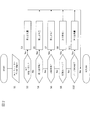
- FIG. 1 is a block diagram showing an epitaxial wafer manufacturing apparatus 1 (hereinafter, also simply referred to as manufacturing apparatus 1) according to an embodiment of the present invention, and the apparatus main body shown at the center is shown by a plan view.
- the manufacturing apparatus 1 of the present embodiment is a so-called normal pressure CVD apparatus, and a wafer transfer chamber 12 in which a pair of reaction furnaces 11 and 11 and a wafer handling robot 121 for handling wafers WF such as single crystal silicon wafers are installed.
- the factory interface 14 takes out the unprocessed wafer WF stored in the cassette case 15 and loads it into the load lock chamber 13 or transfers the processed wafer WF into the load lock chamber 13.
- a transfer device for storing the cassette case 15 is provided.
- the load lock chamber 13 is provided with an airtight door between the wafer transfer chamber 12 and the factory interface 14, and the wafer transfer chamber 12 in an inert gas atmosphere and the atmosphere It functions as a space for replacing the atmosphere gas with the factory interface 14.
- the door on the factory interface 14 side is opened and the door on the wafer transfer chamber 12 is closed.
- the wafer WF is transferred to the load lock chamber 13 via the factory interface 14, and then the door on the factory interface 14 side is closed to replace the load lock chamber 13 with an inert gas atmosphere, and then the wafer transfer chamber 12 side. And the wafer WF is loaded into the wafer transfer chamber 12.
- the door on the wafer transfer chamber 12 side is opened and the door on the factory interface 14 side is closed.
- the door on the wafer transfer chamber 12 side is closed to replace the load lock chamber 13 with the atmosphere, and then the door on the factory interface 14 side is opened to The wafer WF is transferred to the cassette case 15 via the factory interface 14.
- the wafer transfer chamber 12 is comprised of a sealed chamber, one of which is connected to the load lock chamber 13 via an openable and closable door, and the other is connected via an openable and closable gate valve 114. It is connected.
- the wafer WF before processing is transferred from the load lock chamber 13 to the reaction chamber 111
- the wafer WF after processing is transferred from the reaction chamber 111 to the load lock chamber 13.
- a handling robot 121 is installed, and performs a handling operation in accordance with an operation trajectory previously taught by the robot controller 122.
- the robot controller 122 and the first controller 16 that controls the overall control of the epitaxial wafer manufacturing apparatus 1 mutually transmit and receive control signals, and the operation command signal from the first controller 16 is transmitted to the robot controller 122 Then, the robot controller 122 controls the operation of the wafer handling robot 121, and the operation result of the wafer handling robot 121 is transmitted from the robot controller 122 to the first controller 16 so that the first controller 16 can process the wafer
- the operation state of the handling robot 121 is recognized.
- the wafer transfer chamber 12 is supplied with an inert gas from an inert gas supply device (not shown), and after the gas in the wafer transfer chamber 12 is purified by a scrubber (cleaning and dust collecting device) 123 connected to an exhaust port. , Released out of the system.
- a scrubber cleaning and dust collecting device
- the scrubber 123 can use the conventionally well-known pressurized water type scrubber, for example. This type of pressurized water scrubber removes dust contained in the gas by introducing the gas to be exhausted from the exhaust port and spraying pressurized water into a venturi tube or the like.
- the pressurized water of the scrubber 123 is supplied by circulating the water stored in the water storage tank provided in the scrubber with a circulation pump, and the circulation water volume of the circulation pump is controlled by the third controller 124. Control is performed based on a command signal from the first controller 16.
- the pressure of the wafer transfer chamber 12 is lowered by the exhaust function of the scrubber 123, the amount of circulating water by the circulation pump of the scrubber 123 is increased and the pressure of the wafer transfer chamber 12 is increased.
- the amount of circulating water by the circulating pump of the scrubber 123 can be reduced.
- control can also be performed by opening and closing the flow path using a butterfly valve or a needle valve. Control of the pressure of the wafer transfer chamber 12 will be described later.
- an exhaust pump may be provided, and the exhaust amount of the exhaust pump may be controlled by the third controller 124.
- the scrubber 123 and / or the exhaust pump correspond to a first exhaust means according to the present invention.
- the reaction furnace 11 is an apparatus for generating an epitaxial film on the surface of the wafer WF by the CVD method, and includes a reaction chamber 111, and a susceptor 112 for mounting the wafer WF and rotating in the reaction chamber 111 is provided. Further, a gas supply device 113 for supplying hydrogen gas and a source gas (silicon tetrachloride SiCl 4, trichlorosilane SiHCl 3 or the like) for producing an epitaxial film is provided in the reaction chamber 111. Although not shown, a heating lamp for raising the temperature of the wafer WF to a predetermined temperature is provided around the reaction chamber 111.
- a gate valve 114 is provided between the reaction chamber 111 and the wafer transfer chamber 12, and by closing the gate valve 114, the airtightness with the wafer transfer chamber 12 of the reaction chamber 111 is secured.
- Each control of driving of the susceptor 112 of these reactors 11, supply / stop of gas by the gas supply device 113, ON / OFF of the heating lamp, and opening / closing operation of the gate valve 114 is controlled by a command signal from the first controller 16. Ru.
- the manufacturing apparatus 1 of the epitaxial wafer shown in FIG. 1 showed the example which provided a pair of reaction furnaces 11 and 11, one reaction furnace 11 may be sufficient and three or more reaction furnaces may be sufficient.
- the reaction furnace 11 is also provided with a scrubber 115 having a configuration similar to that of the wafer transfer chamber 12. That is, the hydrogen gas or the source gas supplied from the gas supply device 113 is purified by the scrubber (washing and dust collecting device) 115 connected to the exhaust port provided in the reaction chamber, and then released out of the system.
- the scrubber washing and dust collecting device
- the conventionally well-known pressurized water type scrubber can be used, for example.
- the pressurized water scrubber of this type removes the dust contained in the gas to be exhausted by introducing the gas to be exhausted from the exhaust port and spraying the pressurized water into a venturi tube or the like.
- the pressurized water of the scrubber 115 is supplied by circulating the water stored in the water storage tank provided in the scrubber with a circulation pump, and the circulation water volume of the circulation pump is controlled by the second controller 116. Control is performed based on a command signal from the first controller 16.
- the pressure in the reaction chamber 111 is lowered by the exhaust function of the scrubber 115, the amount of circulating water by the circulation pump of the scrubber 115 is increased and the pressure in the reaction chamber 111 is increased, the circulation of the scrubber 115 is reduced.
- the amount of circulating water by the pump can be reduced.
- control is also possible by opening and closing the flow path by a butterfly valve. Control of the pressure of the reaction chamber 111 will be described later.
- an exhaust pump may be provided, and the displacement of the exhaust pump may be controlled by the second controller 116.
- the scrubber 115 and / or the exhaust pump correspond to a second exhaust means according to the present invention.
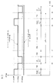
- FIG. 3 is a time chart showing the contents of control executed by the first controller 16 and the second controller 116 of the epitaxial wafer manufacturing apparatus 1 of the present embodiment, and the lower part shows the step of forming the epitaxial film in the reaction furnace 11. .
- Time t0 to time t5 on the horizontal axis represents one cycle of film formation.
- the gate valve 114 is opened, and the wafer WF already processed is taken out using the wafer handling robot 121, and the wafer WF before processing is placed on the susceptor 112 of the reaction chamber 111.
- the process waits from time t4 to time t5, and at time t5 the gate valve 114 At time t5 to t6, the wafer handling robot 121 is used to take out the processed wafer WF at this time and place the wafer WF before the next processing on the susceptor 112 of the reaction chamber 111.
- the above-described scrubbers 115 and 123 are provided in the reaction chamber 111 and the wafer transfer chamber 12, respectively, but they are used only for the original gas purification and have an exhaust function. However, there was no control of exhaust volume.
- the exhaust amount of each of the scrubbers 115 and 123 is associated with the above-described epitaxial film generation step.
- FIG. 2 is a flowchart showing a control procedure executed by the second controller 116 of the epitaxial wafer manufacturing apparatus 1 of the present embodiment, and the upper part of FIG. 3 is from the reaction chamber 111 realized by the control of the second controller 116. It is a time chart which shows transition of gas displacement. The calculation of the flowchart shown in FIG. 2 is performed at predetermined time intervals (for example, 10 msec). The vertical axis in FIG. 3 indicates the displacement of the reaction chamber 111 by the scrubber 115 and the displacement of the wafer transfer chamber 12 by the scrubber 123.
- the pressure of the reaction chamber 111 and the pressure of the wafer transfer chamber 12 Although the pressure varies slightly depending on the amount of gas supplied, the pressure is the same when removing and loading a wafer, and the pressure in the reaction chamber is low during film formation, and the wafer reaction chamber is in purge after film formation. Is a lower pressure. .
- the control of the displacement of the scrubber 123 by the third controller 124 is as shown in the graph of the target displacement of the scrubber 123 (first evacuation means) in FIG.
- the exhaust displacement is controlled to be within a predetermined range (there may be some errors), that is, to be a constant amount.
- the exhaust amount of the scrubber 115 connected to the reaction chamber 111 can be set to three levels of exhaust amount, ie, the first exhaust amount, the second exhaust amount and the third exhaust amount, as shown in FIG.
- the relationship of (2) displacement ⁇ (first displacement) ⁇ (third displacement) is established.
- the difference in pressure of the reaction chamber 111 with respect to the pressure of the wafer transfer chamber 12 can be set based on the exhaust pressure by the exhaust amount controlled by the scrubber 123 by setting of these three levels of exhaust amount.
- the exhaust pressure for the first exhaust volume is -0.4 to -0.6 kPa
- the exhaust pressure for the second exhaust volume is 0 to -0.3 kPa
- the exhaust pressure for the third exhaust volume is -0.7 kPa or more. It is set to become.
- step S1 of FIG. 2 the second controller 116 inputs a control signal from the first controller 16 to the manufacturing apparatus 1.
- the control signal includes a command signal output in each generation process of the epitaxial film shown in the lower part of FIG. 3, and the second controller 116 can recognize which process is currently being executed.
- step S1 If the control signal from the first controller 16 input in step S1 is the removal / insertion of the wafer WF in the reaction chamber 111, the process proceeds to step S3, and circulation is performed so that the exhaust amount by the scrubber 115 becomes the second exhaust amount. Reduce the amount of circulating water in the pump. As a result, as shown from time t0 to t1 in FIG. 3, the pressure of the reaction chamber 111 becomes equal to or approximates to the pressure of the wafer transfer chamber 12 as the displacement of the reaction chamber 111 decreases.
- step S2 when the control signal from the first controller 16 is not the removal / input of the wafer WF in the reaction chamber 111, the process proceeds to step S4, and the control signal from the first controller 16 is the removal / supply of the wafer WF. If it is a subsequent standby signal, the process proceeds to step S5.
- the fact that the standby signal has been input means that the wafer WF has been completely taken out and turned on, and the gate valve 114 is closed.
- step S5 the second controller 116 makes the circulating water amount of the circulation pump medium, so that the displacement of the scrubber 115 becomes the first displacement.
- the exhaust amount from the reaction chamber 111 becomes the same as that in the case of performing the next film forming process, and it is possible to smoothly shift to the film forming process.
- step 4 when the control signal from the first controller 16 is not the standby signal after unloading / loading of the wafer WF, the process proceeds to step S6, and the control signal from the first controller 16 is the film formation processing signal In the case, the process proceeds to step S7.
- step S7 the second controller 116 makes the circulating water amount of the circulation pump medium so that the displacement of the scrubber 115 becomes the first displacement.
- the amount of exhaust from the reaction chamber 111 becomes the amount of exhaust to perform the film forming process. In this state, film formation processing (purge ⁇ temperature rise ⁇ bake ⁇ deposition) of the epitaxial film is performed.
- step 6 if the control signal from the first controller 16 is not an epitaxial film generation processing signal, the process proceeds to step S8, where the control signal from the first controller 16 is a hydrogen gas purge after film formation processing of the epitaxial film. If it is a processing signal of (1), the process proceeds to step S9.
- the fact that the hydrogen gas purge signal is input means that the gate valve 114 is still closed.
- step S9 the second controller 116 increases the circulating water amount of the circulation pump so that the displacement by the scrubber 115 becomes the third displacement. As a result, as shown from time t3 to time t4 in FIG. 3, the amount of exhaust gas from the reaction chamber 111 is increased, so that dust such as particles generated in the reaction chamber 111 does not adhere to the wafer WF. It can be discharged out of the reaction chamber 111 via 115.
- step 8 if the control signal from the first controller 16 is not a processing signal of hydrogen gas purge after the epitaxial film generation processing, the process proceeds to step S10, and the control signal from the first controller 16 is hydrogen gas after purge. If it is a standby signal, the process proceeds to step S11.
- the fact that the standby signal after the hydrogen gas purge is input means that the gate valve 114 is still closed.
- step S11 the second controller 116 makes the circulating water amount of the circulation pump medium, so that the displacement of the scrubber 115 becomes the first displacement. As a result, as shown at times t4 to t5 in FIG.
- step S11 the second controller 116 may reduce the amount of circulating water of the circulation pump so that the displacement of the scrubber 115 becomes the second displacement.
- step S11 if the displacement by the scrubber 115 is made the first displacement, it is possible to balance the removal effect of the dust discharged from the reaction chamber 111 and the reduction of the differential pressure at the moment when the gate valve 114 is opened at time t5.
- the displacement by the scrubber 115 is set to the second displacement in step S11, the removal effect of dust discharged from the reaction chamber 111 is reduced, but the moment when the gate valve 114 is opened at time t5 Differential pressure is significantly reduced, so generation of dust such as particles (that is, soaring) is suppressed, and the effect of suppressing the flow from the wafer transfer chamber 12 to the reaction chamber 111 and adhering to the wafer WF becomes larger. .
- step S10 when the control signal from the first controller 16 is not the standby signal after the hydrogen gas purge, the process returns to step S1 and the above procedure is repeated.
- the epitaxial wafer manufacturing apparatus 1 of the present embodiment focusing on the exhaust function of the scrubbers 115 and 123, and controlling the exhaust amount of each of the scrubbers 115 and 123 in relation to the step of forming the epitaxial film.
- the pressure of the reaction chamber 111 itself and the differential pressure between the reaction chamber 111 and the wafer transfer chamber 12 are controlled, thereby suppressing the adhesion of dust such as particles to the wafer WF.
Landscapes
- Chemical & Material Sciences (AREA)
- Engineering & Computer Science (AREA)
- Materials Engineering (AREA)
- Metallurgy (AREA)
- Organic Chemistry (AREA)
- General Chemical & Material Sciences (AREA)
- Chemical Kinetics & Catalysis (AREA)
- Crystallography & Structural Chemistry (AREA)
- Mechanical Engineering (AREA)
- Chemical Vapour Deposition (AREA)
Abstract
エピタキシャルウェーハの製造装置(1)の反応室(111)からの排気量を、反応室においてエピタキシャル成膜処理を行っている場合には第1排気量に制御し、ゲートバルブ(114)を開いて反応室とウェーハ移載室(12)との間でウェーハ(WF)を投入又は取り出す場合には、第1排気量より小さい第2排気量に制御し、反応室にてエピタキシャル成膜処理を終了したのち、反応室のガスのパージ処理が終了するまでは、第1排気量より大きい第3排気量に制御する。
Description
本発明は、エピタキシャルウェーハの製造装置及び製造方法に関するものである。
エピタキシャル膜を成長させる反応室(プロセスチャンバ)と、反応室と連通して反応室内にウェーハを搬送するウェーハ移載室(トランスファチャンバ)と、反応室と移載室との連通部に設けられ反応室と移載室とのガスの流通を開放・閉止する仕切り可動機構(ゲートバルブ)とを備えたエピタキシャル成長装置を用い、裏面に多結晶シリコン膜を備えたシリコンウェーハの表面側にシリコンエピタキシャル膜を形成するエピタキシャルシリコンウェーハの製造方法が知られている(特許文献1)。
このエピタキシャルウェーハの製造方法では、窒素ガス雰囲気とした移載室内の圧力を、水素ガス雰囲気とした反応室内の圧力よりも0.067kPa~0.267kPa(0.5Torr~2Torr)高めた状態でゲートバルブを開き、移載室内のシリコンウェーハを反応室内に搬送すると共に、移載室内の圧力と反応室内の圧力の差を利用して移載室内の窒素ガスを反応室内に供給する。そして、反応室内に設けたサセプタにシリコンウェーハを載置し、ゲートバルブを閉じて反応室内への窒素ガスの供給を停止した後、シリコンウェーハ表面にシリコンエピタキシャル膜を形成する。
しかしながら、反応室と移載室との差圧を上記従来技術のように一律に設定すると、設定された差圧が大きいと、ゲートバルブを開いた時にパーティクルが巻き上がり易くなる一方で、設定された差圧が小さくするために排気圧力を下げるとパーティクルの排気不足になる。いずれの場合も、LPD(Light Point Defect,光散乱輝点欠陥)品質が低下するという問題がある。
本発明が解決しようとする課題は、LPD品質を高めることができるエピタキシャルウェーハの製造装置及び製造方法を提供することである。
本発明は、ウェーハにエピタキシャル膜を成長させる反応室と、
前記反応室と連通するウェーハ移載室と、
前記反応室と前記移載室との連通部に設けられ反応室と移載室とのガスの流通を開閉するゲートバルブと、
前記ウェーハ移載室に設けられ、処理前のウェーハを前記移載室から前記反応室に投入し、処理後のウェーハを前記反応室から前記ウェーハ移載室へ取り出すウェーハ移載手段と、
前記ウェーハ移載室から前記反応室へ前記ウェーハを投入し、前記反応室においてエピタキシャル成膜処理を行ったのち、前記反応室から前記ウェーハ移載室へ前記ウェーハを取り出す制御を実行する第1制御手段と、
前記ウェーハ移載室のガスを排気する第1排気手段と、
前記反応室のガスを排気する第2排気手段と、
前記第1排気手段及び前記第2排気手段による排気量を制御する第2制御手段と、を備え、
前記第2制御手段は、
前記第1排気手段による排気量を所定の範囲に制御するとともに、
前記第1制御手段によるエピタキシャル膜の成長工程の制御信号を入力し、当該制御信号に基づいて、
前記第2排気手段による排気量を、
前記反応室においてエピタキシャル成膜処理を行っている場合には、第1排気量に制御し、
前記ゲートバルブを開いて前記反応室と前記ウェーハ移載室との間で前記ウェーハを投入又は取り出す場合には、前記第1排気量より小さい第2排気量に制御し、
前記反応室にてエピタキシャル成膜処理を終了したのち、前記反応室のガスのパージ処理が終了するまでは、前記第1排気量より大きい第3排気量に制御するエピタキシャルウェーハの製造装置である。
前記反応室と連通するウェーハ移載室と、
前記反応室と前記移載室との連通部に設けられ反応室と移載室とのガスの流通を開閉するゲートバルブと、
前記ウェーハ移載室に設けられ、処理前のウェーハを前記移載室から前記反応室に投入し、処理後のウェーハを前記反応室から前記ウェーハ移載室へ取り出すウェーハ移載手段と、
前記ウェーハ移載室から前記反応室へ前記ウェーハを投入し、前記反応室においてエピタキシャル成膜処理を行ったのち、前記反応室から前記ウェーハ移載室へ前記ウェーハを取り出す制御を実行する第1制御手段と、
前記ウェーハ移載室のガスを排気する第1排気手段と、
前記反応室のガスを排気する第2排気手段と、
前記第1排気手段及び前記第2排気手段による排気量を制御する第2制御手段と、を備え、
前記第2制御手段は、
前記第1排気手段による排気量を所定の範囲に制御するとともに、
前記第1制御手段によるエピタキシャル膜の成長工程の制御信号を入力し、当該制御信号に基づいて、
前記第2排気手段による排気量を、
前記反応室においてエピタキシャル成膜処理を行っている場合には、第1排気量に制御し、
前記ゲートバルブを開いて前記反応室と前記ウェーハ移載室との間で前記ウェーハを投入又は取り出す場合には、前記第1排気量より小さい第2排気量に制御し、
前記反応室にてエピタキシャル成膜処理を終了したのち、前記反応室のガスのパージ処理が終了するまでは、前記第1排気量より大きい第3排気量に制御するエピタキシャルウェーハの製造装置である。
本発明において、前記第2制御手段は、
前記反応室にてエピタキシャル成膜処理を終了し、前記反応室のガスのパージ処理が終了した時点から、前記ゲートバルブを開いて前記ウェーハを前記ウェーハ移載室へ取り出す時点までの間は、前記第2排気手段による排気量を、前記第1排気量又は第2排気量に制御することがより好ましい。
前記反応室にてエピタキシャル成膜処理を終了し、前記反応室のガスのパージ処理が終了した時点から、前記ゲートバルブを開いて前記ウェーハを前記ウェーハ移載室へ取り出す時点までの間は、前記第2排気手段による排気量を、前記第1排気量又は第2排気量に制御することがより好ましい。
本発明において、前記第1排気手段で制御される排気量による排気圧を基準とする、
前記第1排気量による排気圧は、-0.4~-0.6kPa、
前記第2排気量による排気圧は、0~-0.3kPa、
前記第3排気量による排気圧は、-0.7kPa以上とすることができる。
前記第1排気量による排気圧は、-0.4~-0.6kPa、
前記第2排気量による排気圧は、0~-0.3kPa、
前記第3排気量による排気圧は、-0.7kPa以上とすることができる。
本発明は、ウェーハにエピタキシャル膜を成長させる反応室と、前記反応室と連通するウェーハ移載室と、前記反応室と前記移載室との連通部に設けられ反応室と移載室とのガスの流通を開閉するゲートバルブと、前記ウェーハ移載室に設けられ、処理前のウェーハを前記移載室から前記反応室に投入し、処理後のウェーハを前記反応室から前記ウェーハ移載室へ取り出すウェーハ移載手段と、を備えるエピタキシャルウェーハの製造装置を用いたエピタキシャルウェーハの製造方法において、
前記ウェーハ移載室の圧力を所定の範囲に制御するとともに、
前記反応室の圧力を、
前記反応室においてエピタキシャル成膜処理を行っている場合には、第1圧力に制御し、
前記ゲートバルブを開いて前記反応室と前記ウェーハ移載室との間で前記ウェーハを投入又は取り出す場合には、前記第1圧力より高い第2圧力に制御し、
前記反応室にてエピタキシャル成膜処理を終了したのち、前記反応室のガスのパージ処理が終了するまでは、前記第1圧力より低い第3圧力に制御するエピタキシャルウェーハの製造方法である。
前記ウェーハ移載室の圧力を所定の範囲に制御するとともに、
前記反応室の圧力を、
前記反応室においてエピタキシャル成膜処理を行っている場合には、第1圧力に制御し、
前記ゲートバルブを開いて前記反応室と前記ウェーハ移載室との間で前記ウェーハを投入又は取り出す場合には、前記第1圧力より高い第2圧力に制御し、
前記反応室にてエピタキシャル成膜処理を終了したのち、前記反応室のガスのパージ処理が終了するまでは、前記第1圧力より低い第3圧力に制御するエピタキシャルウェーハの製造方法である。
本発明において、前記反応室にてエピタキシャル成膜処理を終了し、前記反応室のガスのパージ処理が終了した時点から、前記ゲートバルブを開いて前記ウェーハを前記ウェーハ移載室へ取り出す時点までの間は、前記反応室の圧力を、前記第1圧力又は第2圧力に制御することがより好ましい。
本発明によれば、ゲートバルブを開いて反応室とウェーハ移載室との間でウェーハを投入又は取り出す場合には、エピタキシャル膜の生成時の第1排気量より小さい第2排気量に制御するので、反応室とウェーハ移載室との差圧が小さくなり、ウェーハ移載室のパーティクルなどの塵埃が反応室へ流れてウェーハに付着するのを抑制することができる。一方において、反応室にてエピタキシャル成膜処理を終了したのち、反応室のガスのパージ処理が終了するまでは、エピタキシャル膜の生成時の第1排気量より大きい第3排気量に制御するので、反応室内で発生したパーティクルなどの塵埃がウェーハに付着することなく反応室外へ排出することができる。この結果、LPD品質を高めることができる。
以下、本発明の実施形態を図面に基づいて説明する。図1は、本発明の実施形態に係るエピタキシャルウェーハの製造装置1(以下、単に製造装置1ともいう。)を示すブロック図であり、中央に示す装置本体は平面図により示したものである。本実施形態の製造装置1は、いわゆる常圧CVD装置であり、一対の反応炉11,11と、単結晶シリコンウェーハなどのウェーハWFをハンドリングするウェーハハンドリングロボット121が設置されたウェーハ移載室12と、一対のロードロック室13と、ファクトリインターフェース14と、複数枚のウェーハWFを収納したカセットケース15と、を備える。図示は省略するが、ファクトリインターフェース14には、カセットケース15に収納された処理前のウェーハWFを取り出してロードロック室13へ投入したり、ロードロック室13へ搬送された処理後のウェーハWFをカセットケース15へ収納したりする移載装置が設けられている。
ロードロック室13は、ウェーハ移載室12との間及びファクトリインターフェース14との間にそれぞれ気密性を有するドアが設けられ、不活性ガス雰囲気とされたウェーハ移載室12と、大気雰囲気とされたファクトリインターフェース14との間で、雰囲気ガスを置換するスペースとして機能する。たとえば、カセットケース15から処理前のウェーハWFをウェーハ移載室12に搬送する場合には、ファクトリインターフェース14側のドアを開き、ウェーハ移載室12側のドアを閉じた状態で、カセットケース15のウェーハWFを、ファクトリインターフェース14を介してロードロック室13に搬送したのち、ファクトリインターフェース14側のドアを閉じて当該ロードロック室13を不活性ガス雰囲気に置換し、その後ウェーハ移載室12側のドアを開いて当該ウェーハWFをウェーハ移載室12に搬入する。逆に、ウェーハ移載室12から処理後のウェーハWFをカセットケース15へ搬送する場合には、ウェーハ移載室12側のドアを開き、ファクトリインターフェース14側のドアを閉じた状態で、ウェーハ移載室12のウェーハWFをロードロック室13に搬送したのち、ウェーハ移載室12側のドアを閉じて当該ロードロック室13を大気雰囲気に置換し、その後ファクトリインターフェース14側のドアを開いて当該ウェーハWFを、ファクトリインターフェース14を介してカセットケース15に搬送する。
ウェーハ移載室12は、密閉されたチャンバからなり、一方がロードロック室13と開閉可能な気密性を有するドアを介して接続され、他方が気密性を有する開閉可能なゲートバルブ114を介して接続されている。ウェーハ移載室12には、上述したように、処理前のウェーハWFをロードロック室13から反応室111へ搬送するとともに、処理後のウェーハWFを反応室111からロードロック室13へ搬送するウェーハハンドリングロボット121が設置され、ロボットコントローラ122により予め教示された動作軌跡に従ってハンドリング操作を行う。なお、ロボットコントローラ122と、エピタキシャルウェーハの製造装置1の全体の制御を統括する第1コントローラ16とは、相互に制御信号を送受信し、第1コントローラ16からの動作指令信号がロボットコントローラ122に送信されると、ロボットコントローラ122はウェーハハンドリングロボット121の動作を制御し、当該ウェーハハンドリングロボット121の動作結果がロボットコントローラ122から第1コントローラ16へ送信されることで、当該第1コントローラ16は、ウェーハハンドリングロボット121の動作状態を認識する。
ウェーハ移載室12には、図示しない不活性ガス供給装置から不活性ガスが供給され、排気口に接続されたスクラバ(洗浄集塵装置)123によってウェーハ移載室12のガスが浄化されたのち、系外へ放出される。スクラバ123は、詳細な図示は省略するが、たとえば従来公知の加圧水式スクラバを用いることができる。この種の加圧水式スクラバは、ベンチュリー管などに、排気口からの排気すべきガスを導入するとともに加圧水を噴霧することで、ガスに含まれた塵埃を除去する。これに加えて、ベンチュリー管にガスとともに加圧水を供給すると、エジェクタ効果によって排気口からのガスが吸引されるので、一種の排気装置としても機能する。スクラバ123の加圧水は、スクラバに設けられた貯水タンクの貯水を循環ポンプで循環させることで供給されるが、循環ポンプの循環水量は第3コントローラ124により制御され、第3コントローラ124による循環ポンプの制御は、第1コントローラ16からの指令信号に基づいて実行される。なお、たとえば、スクラバ123の排気機能によりウェーハ移載室12の圧力を低くする場合には、スクラバ123の循環ポンプによる循環水量を増加させ、ウェーハ移載室12の圧力を高くする場合には、スクラバ123の循環ポンプによる循環水量を減少させることができる。その他にも圧力を変化させるにはバタフライバルブやニードルバルブ等による流路の開閉でも制御は可能である。ウェーハ移載室12の圧力の制御については後述する。なお、スクラバ123に代えて又はこれに加えて、排気ポンプを設け、当該排気ポンプの排気量を第3コントローラ124で制御するように構成してもよい。これらスクラバ123及び/又は排気ポンプが、本発明に係る第1排気手段に相当する。
反応炉11は、CVD法によりウェーハWFの表面にエピタキシャル膜を生成するための装置であって、反応室111を備え、当該反応室111内にウェーハWFを載置して回転するサセプタ112が設けられ、また反応室111に水素ガス及びエピタキシャル膜を生成するための原料ガス(四塩化ケイ素SiCl4やトリクロロシランSiHCl3など)を供給するガス供給装置113が設けられている。また図示は省略するが、反応室111の周囲には、ウェーハWFを所定温度に昇温するための加熱ランプが設けられている。さらに、反応室111とウェーハ移載室12との間には、ゲートバルブ114が設けられ、ゲートバルブ114を閉塞することで反応室111のウェーハ移載室12との気密性が確保される。これら反応炉11のサセプタ112の駆動、ガス供給装置113によるガスの供給・停止、加熱ランプのON/OFF、ゲートバルブ114の開閉動作の各制御は、第1コントローラ16からの指令信号により制御される。なお、図1に示すエピタキシャルウェーハの製造装置1は、一対の反応炉11,11を設けた例を示したが、一つの反応炉11でもよく、3つ以上の反応炉でもよい。
反応炉11にも、ウェーハ移載室12と同様の構成を有するスクラバ115が設けられている。すなわち、ガス供給装置113から供給された水素ガス又は原料ガスは、反応室に設けられた排気口に接続されたスクラバ(洗浄集塵装置)115によって浄化されたのち、系外へ放出される。スクラバ115についても、詳細な図示は省略するが、たとえば従来公知の加圧水式スクラバを用いることができる。この種の加圧水式スクラバは、ベンチュリー管などに、排気口からの排気すべきガスを導入するとともに加圧水を噴霧することで、排気するガスに含まれた塵埃を除去する。これに加えて、ベンチュリー管にガスとともに加圧水を供給すると、エジェクタ効果によって排気口からのガスが吸引されるので、一種の排気装置としても機能する。スクラバ115の加圧水は、スクラバに設けられた貯水タンクの貯水を循環ポンプで循環させることで供給されるが、循環ポンプの循環水量は第2コントローラ116により制御され、第2コントローラ116による循環ポンプの制御は、第1コントローラ16からの指令信号に基づいて実行される。なお、たとえば、スクラバ115の排気機能により反応室111の圧力を低くする場合には、スクラバ115の循環ポンプによる循環水量を増加させ、反応室111の圧力を高くする場合には、スクラバ115の循環ポンプによる循環水量を減少させることができる。その他にも圧力を変化させるにはバタフライバルブによる流路の開閉でも制御は可能である。反応室111の圧力の制御については後述する。なお、スクラバ115に代えて又はこれに加えて、排気ポンプを設け、当該排気ポンプの排気量を第2コントローラ116で制御するように構成してもよい。これらスクラバ115及び/又は排気ポンプが、本発明に係る第2排気手段に相当する。
反応炉11におけるエピタキシャル膜の生成の手順を、図3を参照して説明する。図3は、本実施形態のエピタキシャルウェーハの製造装置1の第1コントローラ16及び第2コントローラ116で実行される制御内容を示すタイムチャートであり、下部に反応炉11におけるエピタキシャル膜の生成工程を示す。横軸の時間t0から時間t5が成膜の1サイクルを示す。まず、時間t0において、ゲートバルブ114を開き、ウェーハハンドリングロボット121を用いて、前回の処理済みのウェーハWFを取り出すとともに処理前のウェーハWFを反応室111のサセプタ112に載置する。時間t1においてゲートバルブ114を閉じ、時間t2まで待機したのち、時間t2において、ガス供給装置113により反応室111に水素ガスを供給して反応室111を水素ガス雰囲気とする。次いで加熱ランプをONして反応室111のウェーハWFを所定温度に昇温し、必要に応じてエッチングや熱処理などの前処理を施したのち、ガス供給装置113により原料ガスを流量および/又は供給時間を制御しながら供給する。これにより、時間t3においてウェーハWFの表面にエピタキシャル膜が生成される。そして、時間t3において、ガス供給装置113により反応室111に再び水素ガスを供給して反応室111を水素ガス雰囲気に置換したのち、時間t4から時間t5まで待機し、時間t5においてゲートバルブ114を開き、時間t5~t6において、ウェーハハンドリングロボット121を用いて、今回の処理済みのウェーハWFを取り出すとともに次の処理前のウェーハWFを反応室111のサセプタ112に載置する。
従来の常圧CVD装置では、反応室111及びウェーハ移載室12のそれぞれに、上述したスクラバ115,123は設けられていたが、本来のガス浄化のためにのみ用いられ、排気機能は備えているものの、排気量の制御は何ら行われていなかった。これに対して、本実施形態のエピタキシャルウェーハの製造装置1においては、スクラバ115,123が有する排気機能に着目し、上述したエピタキシャル膜の生成工程に関連付けて、各スクラバ115,123の排気量を制御することにより、反応室111自体の圧力及び反応室111とウェーハ移載室12との差圧を制御し、これによりパーティクルなどの塵埃がウェーハWFに付着するのを抑制する。この具体的制御を図2及び図3を参照して説明する。
図2は、本実施形態のエピタキシャルウェーハの製造装置1の第2コントローラ116で実行される制御手順を示すフローチャート、図3の上部が当該第2コントローラ116の制御により実現される反応室111からのガス排気量の遷移を示すタイムチャートである。図2に示すフローチャートの演算は、所定時間間隔(たとえば10msec)で実行される。なお、図3の縦軸は、反応室111からのスクラバ115による排気量及びウェーハ移載室12からのスクラバ123による排気量を示しているので、反応室111及びウェーハ移載室12の圧力の大小は、供給されるガス量により若干の変動は有るものの、ウェーハを取出・投入するときには同等の圧力となり、成膜中には、反応室が低い圧力となり、成膜後パージ中はウェーハ反応室がさらに低い圧力となる。
。なお、本実施形態のエピタキシャルウェーハの製造装置1においては、第3コントローラ124によるスクラバ123の排気量の制御は、図3のスクラバ123(第1排気手段)の目標排気量のグラフに示すように、当該排気量が所定の範囲に入るように(多少の誤差はあってもよい)、すなわち一定量になるように制御されるものとする。また、反応室111に接続されたスクラバ115による排気量は、第1排気量、第2排気量及び第3排気量という3水準の排気量の設定が可能とされ、図3に示すように第2排気量<第1排気量<第3排気量の関係とされている。さらに特に限定はされないが、これら3水準の排気量の設定により、ウェーハ移載室12の圧力に対する反応室111の圧力の差は、スクラバ123で制御される排気量による排気圧を基準にすると、第1排気量による排気圧は、-0.4~-0.6kPa、第2排気量による排気圧は、0~-0.3kPa、第3排気量による排気圧は、-0.7kPa以上となるように設定されている。
。なお、本実施形態のエピタキシャルウェーハの製造装置1においては、第3コントローラ124によるスクラバ123の排気量の制御は、図3のスクラバ123(第1排気手段)の目標排気量のグラフに示すように、当該排気量が所定の範囲に入るように(多少の誤差はあってもよい)、すなわち一定量になるように制御されるものとする。また、反応室111に接続されたスクラバ115による排気量は、第1排気量、第2排気量及び第3排気量という3水準の排気量の設定が可能とされ、図3に示すように第2排気量<第1排気量<第3排気量の関係とされている。さらに特に限定はされないが、これら3水準の排気量の設定により、ウェーハ移載室12の圧力に対する反応室111の圧力の差は、スクラバ123で制御される排気量による排気圧を基準にすると、第1排気量による排気圧は、-0.4~-0.6kPa、第2排気量による排気圧は、0~-0.3kPa、第3排気量による排気圧は、-0.7kPa以上となるように設定されている。
図2のステップS1において、第2コントローラ116は、第1コントローラ16から製造装置1への制御信号を入力する。この制御信号には、図3の下部示すエピタキシャル膜の各生成工程において出力される指令信号が含まれ、現在どの工程を実行しているのかを第2コントローラ116が認識できる。
ステップS1において入力した第1コントローラ16からの制御信号が、反応室111のウェーハWFの取出/投入である場合は、ステップS3へ進み、スクラバ115による排気量が第2排気量になるように循環ポンプの循環水量を減少させる。これにより、図3の時間t0~t1に示すように、反応室111からの排気量が減少することで当該反応室111の圧力がウェーハ移載室12の圧力に等しくなるか近似する。この結果、ゲートバルブ114を開いた瞬間の圧力変動に伴うパーティクルなどの塵埃の発生(つまり舞い上がり)が抑制でき、かつ、ウェーハ移載室12のパーティクルなどの塵埃が反応室111へ流れてウェーハWFに付着するのを抑制することができる。
ステップS2において、第1コントローラ16からの制御信号が、反応室111のウェーハWFの取出/投入ではない場合は、ステップS4へ進み、第1コントローラ16からの制御信号が、ウェーハWFの取り出し/投入後の待機信号である場合はステップS5へ進む。この待機信号が入力されたということは、ウェーハWFの取出/投入が完了してゲートバルブ114が閉じた状態となっている。ステップS5において、第2コントローラ116は、スクラバ115による排気量が第1排気量になるように循環ポンプの循環水量を中程度にする。これにより、図3の時間t1~t2に示すように、反応室111からの排気量が次の成膜工程を行う場合と同じ排気量となり、円滑に成膜工程に遷移することができる。
ステップ4において、第1コントローラ16からの制御信号が、ウェーハWFの取出/投入後の待機信号ではない場合は、ステップS6へ進み、第1コントローラ16からの制御信号が、成膜処理信号である場合はステップS7へ進む。ステップS7において、第2コントローラ116は、スクラバ115による排気量が第1排気量になるように循環ポンプの循環水量を中程度にする。これにより、図3の時間t2~t3に示すように、反応室111からの排気量が成膜工程を行う排気量となる。この状態で、エピタキシャル膜の成膜処理(パージ→昇温→ベーク→デポ)が行われる。
ステップ6において、第1コントローラ16からの制御信号が、エピタキシャル膜の生成処理信号ではない場合は、ステップS8へ進み、第1コントローラ16からの制御信号
が、エピタキシャル膜の成膜処理後の水素ガスパージの処理信号である場合はステップS9へ進む。この水素ガスパージ信号が入力されたということは、未だゲートバルブ114が閉じている状態である。ステップS9において、第2コントローラ116は、スクラバ115による排気量が第3排気量になるように循環ポンプの循環水量を増加させる。これにより、図3の時間t3~t4に示すように、反応室111からの排気量が増加することで、反応室111内で発生したパーティクルなどの塵埃が、ウェーハWFに付着することなく、スクラバ115を介して反応室111外へ排出することができる。
が、エピタキシャル膜の成膜処理後の水素ガスパージの処理信号である場合はステップS9へ進む。この水素ガスパージ信号が入力されたということは、未だゲートバルブ114が閉じている状態である。ステップS9において、第2コントローラ116は、スクラバ115による排気量が第3排気量になるように循環ポンプの循環水量を増加させる。これにより、図3の時間t3~t4に示すように、反応室111からの排気量が増加することで、反応室111内で発生したパーティクルなどの塵埃が、ウェーハWFに付着することなく、スクラバ115を介して反応室111外へ排出することができる。
ステップ8において、第1コントローラ16からの制御信号が、エピタキシャル膜の生成処理後の水素ガスパージの処理信号ではない場合は、ステップS10へ進み、第1コントローラ16からの制御信号が、水素ガスパージ後の待機信号である場合はステップS11へ進む。この水素ガスパージ後の待機信号が入力されたということは、未だゲートバルブ114が閉じている状態である。ステップS11において、第2コントローラ116は、スクラバ115による排気量が第1排気量になるように循環ポンプの循環水量を中程度にする。これにより、図3の時間t4~t5に示すように、次のウェーハWFの取出/投入の工程で実行される第2排気量に近づくので、時間t5においてゲートバルブ114を開いた瞬間におけるウェーハ移載室12と反応室111との圧力差を小さくすることができる。なお、ステップS11において、第2コントローラ116は、スクラバ115による排気量が第2排気量になるように循環ポンプの循環水量を減少させてもよい。ステップS11において、スクラバ115による排気量を第1排気量にすると、反応室111から排出される塵埃の除去効果と時間t5においてゲートバルブ114を開いた瞬間の差圧の減少とのバランスが取れるという効果があるのに対し、ステップS11において、スクラバ115による排気量を第2排気量にすると、反応室111から排出される塵埃の除去効果は減少するが、時間t5においてゲートバルブ114を開いた瞬間の差圧が著しく小さくなるのでパーティクルなどの塵埃の発生(つまり舞い上がり)が抑制され、且つ、ウェーハ移載室12から反応室111に流れてウェーハWFに付着するのを抑制する効果はより大きくなる。
ステップS10において、第1コントローラ16からの制御信号が、水素ガスパージ後の待機信号ではない場合はステップS1へ戻り、以下、以上の手順を繰り返す。
以上のとおり、本実施形態のエピタキシャルウェーハの製造装置1においては、スクラバ115,123が有する排気機能に着目し、エピタキシャル膜の生成工程に関連付けて、各スクラバ115,123の排気量を制御することにより、反応室111自体の圧力及び反応室111とウェーハ移載室12との差圧を制御し、これによりパーティクルなどの塵埃がウェーハWFに付着するのを抑制する。このように制御した実施例のエピタキシャルウェーハ(N=1413枚)と、スクラバ115,123の排気量を一定とした場合の比較例のエピタキシャルウェーハ(N=1389枚)を実際に製造し、エピ欠陥をSP2のDCO(Darkfield Composite Oblique)モードで200nm以上にて評価したところ、比較例は0.132個/WFであったのに対し、実施例は0.118個/WFであった。
1…エピタキシャルウェーハの製造装置
11…反応炉
111…反応室
112…サセプタ
113…ガス供給装置
114…ゲートバルブ
115…スクラバ
116…第2コントローラ
12…ウェーハ移載室
121…ウェーハハンドリングロボット
122…ロボットコントローラ
123…スクラバ
124…第3コントローラ
13…ロードロック室
14…ファクトリインターフェース
15…カセットケース
16…第1コントローラ
WF…ウェーハ
11…反応炉
111…反応室
112…サセプタ
113…ガス供給装置
114…ゲートバルブ
115…スクラバ
116…第2コントローラ
12…ウェーハ移載室
121…ウェーハハンドリングロボット
122…ロボットコントローラ
123…スクラバ
124…第3コントローラ
13…ロードロック室
14…ファクトリインターフェース
15…カセットケース
16…第1コントローラ
WF…ウェーハ
Claims (5)
- ウェーハにエピタキシャル膜を成長させる反応室と、
前記反応室と連通するウェーハ移載室と、
前記反応室と前記ウェーハ移載室との連通部に設けられ反応室とウェーハ移載室とのガスの流通を開閉するゲートバルブと、
前記ウェーハ移載室に設けられ、処理前のウェーハを前記ウェーハ移載室から前記反応室に投入し、処理後のウェーハを前記反応室から前記ウェーハ移載室へ取り出すウェーハ移載手段と、
前記ウェーハ移載室から前記反応室へ前記ウェーハを投入し、前記反応室においてエピタキシャル成膜処理を行ったのち、前記反応室から前記ウェーハ移載室へ前記ウェーハを取り出す制御を実行する第1制御手段と、
前記ウェーハ移載室のガスを排気する第1排気手段と、
前記反応室のガスを排気する第2排気手段と、
前記第1排気手段及び前記第2排気手段による排気量を制御する第2制御手段と、を備え、
前記第2制御手段は、
前記第1排気手段による排気量を所定の範囲に制御するとともに、
前記第1制御手段によるエピタキシャル膜の成長工程の制御信号を入力し、当該制御信号に基づいて、
前記第2排気手段による排気量を、
前記反応室においてエピタキシャル成膜処理を行っている場合には、第1排気量に制御し、
前記ゲートバルブを開いて前記反応室と前記ウェーハ移載室との間で前記ウェーハを投入又は取り出す場合には、前記第1排気量より小さい第2排気量に制御し、
前記反応室にてエピタキシャル成膜処理を終了したのち、前記反応室のガスのパージ処理が終了するまでは、前記第1排気量より大きい第3排気量に制御するエピタキシャルウェーハの製造装置。 - 前記第2制御手段は、
前記反応室にてエピタキシャル成膜処理を終了し、前記反応室のガスのパージ処理が終了した時点から、前記ゲートバルブを開いて前記ウェーハを前記ウェーハ移載室へ取り出す時点までの間は、前記第2排気手段による排気量を、前記第1排気量又は第2排気量に制御する請求項1に記載のエピタキシャルウェーハの製造装置。 - 前記第1排気手段で制御される排気量による排気圧を基準とする、
前記第1排気量による排気圧は、-0.4~-0.6kPa、
前記第2排気量による排気圧は、0~-0.3kPa、
前記第3排気量による排気圧は、-0.7kPa以上である請求項1又は2に記載のエピタキシャルウェーハの製造装置。 - ウェーハにエピタキシャル膜を成長させる反応室と、前記反応室と連通するウェーハ移載室と、前記反応室と前記ウェーハ移載室との連通部に設けられ反応室とウェーハ移載室とのガスの流通を開閉するゲートバルブと、前記ウェーハ移載室に設けられ、処理前のウェーハを前記ウェーハ移載室から前記反応室に投入し、処理後のウェーハを前記反応室から前記ウェーハ移載室へ取り出すウェーハ移載手段と、を備えるエピタキシャルウェーハの製造装置を用いたエピタキシャルウェーハの製造方法において、
前記ウェーハ移載室の圧力を所定の範囲に制御するとともに、
前記反応室の圧力を、
前記反応室においてエピタキシャル成膜処理を行っている場合には、第1圧力に制御し、
前記ゲートバルブを開いて前記反応室と前記ウェーハ移載室との間で前記ウェーハを投入又は取り出す場合には、前記第1圧力より高い第2圧力に制御し、
前記反応室にてエピタキシャル成膜処理を終了したのち、前記反応室のガスのパージ処理が終了するまでは、前記第1圧力より低い第3圧力に制御するエピタキシャルウェーハの製造方法。 - 前記反応室にてエピタキシャル成膜処理を終了し、前記反応室のガスのパージ処理が終了した時点から、前記ゲートバルブを開いて前記ウェーハを前記ウェーハ移載室へ取り出す時点までの間は、前記反応室の圧力を、前記第1圧力又は前記第2圧力に制御する請求項4に記載のエピタキシャルウェーハの製造方法。
Priority Applications (4)
| Application Number | Priority Date | Filing Date | Title |
|---|---|---|---|
| DE112018006089.6T DE112018006089T5 (de) | 2017-12-28 | 2018-11-05 | Vorrichtung und verfahren zur herstellung von epitaxialwafern |
| US16/758,599 US11414780B2 (en) | 2017-12-28 | 2018-11-05 | Apparatus and method for manufacturing epitaxial wafer |
| KR1020207013044A KR102411407B1 (ko) | 2017-12-28 | 2018-11-05 | 에피택셜 웨이퍼의 제조 장치 및 제조 방법 |
| CN201880068636.6A CN111213223B (zh) | 2017-12-28 | 2018-11-05 | 外延片的制造装置及制造方法 |
Applications Claiming Priority (2)
| Application Number | Priority Date | Filing Date | Title |
|---|---|---|---|
| JP2017254019A JP6485536B1 (ja) | 2017-12-28 | 2017-12-28 | エピタキシャルウェーハの製造装置及び製造方法 |
| JP2017-254019 | 2017-12-28 |
Publications (1)
| Publication Number | Publication Date |
|---|---|
| WO2019130826A1 true WO2019130826A1 (ja) | 2019-07-04 |
Family
ID=65802277
Family Applications (1)
| Application Number | Title | Priority Date | Filing Date |
|---|---|---|---|
| PCT/JP2018/041041 Ceased WO2019130826A1 (ja) | 2017-12-28 | 2018-11-05 | エピタキシャルウェーハの製造装置及び製造方法 |
Country Status (7)
| Country | Link |
|---|---|
| US (1) | US11414780B2 (ja) |
| JP (1) | JP6485536B1 (ja) |
| KR (1) | KR102411407B1 (ja) |
| CN (1) | CN111213223B (ja) |
| DE (1) | DE112018006089T5 (ja) |
| TW (1) | TWI674622B (ja) |
| WO (1) | WO2019130826A1 (ja) |
Families Citing this family (4)
| Publication number | Priority date | Publication date | Assignee | Title |
|---|---|---|---|---|
| JP7192756B2 (ja) * | 2019-12-19 | 2022-12-20 | 株式会社Sumco | 気相成長装置及び気相成長方法 |
| JP7279630B2 (ja) * | 2019-12-26 | 2023-05-23 | 株式会社Sumco | 気相成長装置 |
| KR102525514B1 (ko) * | 2021-01-28 | 2023-04-25 | 에스케이실트론 주식회사 | 반응성 미세입자의 발생을 억제하는 에피택셜 성장장치 및 에피택셜 성장방법 |
| CN119764210B (zh) * | 2024-11-18 | 2025-11-18 | 西安奕斯伟材料科技股份有限公司 | 外延生长设备、外延生长方法以及外延晶圆 |
Citations (13)
| Publication number | Priority date | Publication date | Assignee | Title |
|---|---|---|---|---|
| JPH04162709A (ja) * | 1990-10-26 | 1992-06-08 | Fujitsu Ltd | 半導体製造装置および反応処理方法 |
| JPH0529263A (ja) * | 1991-07-18 | 1993-02-05 | Mitsubishi Electric Corp | 半導体製造装置 |
| JPH05259098A (ja) * | 1992-03-11 | 1993-10-08 | Tokyo Electron Ltd | 真空排気方法 |
| JPH1074817A (ja) * | 1996-08-30 | 1998-03-17 | Kokusai Electric Co Ltd | ウェハ処理方法 |
| JP2000306903A (ja) * | 1999-04-16 | 2000-11-02 | Kokusai Electric Co Ltd | 基板処理装置 |
| JP2001345279A (ja) * | 2000-03-29 | 2001-12-14 | Hitachi Kokusai Electric Inc | 半導体製造方法、基板処理方法、及び半導体製造装置 |
| JP2003163212A (ja) * | 2001-11-27 | 2003-06-06 | Nec Electronics Corp | 半導体装置の製造方法 |
| WO2005050725A1 (ja) * | 2003-11-20 | 2005-06-02 | Hitachi Kokusai Electric Inc. | 半導体装置の製造方法及び基板処理装置 |
| JP2007308730A (ja) * | 2006-05-16 | 2007-11-29 | Ulvac Japan Ltd | 真空処理装置および真空処理方法 |
| JP2012238772A (ja) * | 2011-05-13 | 2012-12-06 | Sharp Corp | 反応室開放方法、及び気相成長装置 |
| JP2013232455A (ja) * | 2012-04-27 | 2013-11-14 | Sumco Corp | エピタキシャルシリコンウェーハの製造方法 |
| JP2015070097A (ja) * | 2013-09-27 | 2015-04-13 | 芝浦メカトロニクス株式会社 | 基板処理装置及び基板処理方法 |
| JP2016111226A (ja) * | 2014-12-08 | 2016-06-20 | 株式会社Sumco | エピタキシャルシリコンウェーハの製造方法、および、気相成長装置 |
Family Cites Families (4)
| Publication number | Priority date | Publication date | Assignee | Title |
|---|---|---|---|---|
| JPH10214828A (ja) * | 1997-01-30 | 1998-08-11 | Nec Kansai Ltd | 半導体製造装置 |
| JP3037280B2 (ja) * | 1998-09-24 | 2000-04-24 | 九州日本電気株式会社 | 半導体の製造方法及び製造装置 |
| KR100647442B1 (ko) * | 2000-06-07 | 2006-11-17 | 주성엔지니어링(주) | 원자층 증착법을 이용한 박막 형성방법 |
| JP6055637B2 (ja) * | 2012-09-20 | 2016-12-27 | 株式会社日立国際電気 | クリーニング方法、半導体装置の製造方法、基板処理装置及びプログラム |
-
2017
- 2017-12-28 JP JP2017254019A patent/JP6485536B1/ja active Active
-
2018
- 2018-11-05 US US16/758,599 patent/US11414780B2/en active Active
- 2018-11-05 CN CN201880068636.6A patent/CN111213223B/zh active Active
- 2018-11-05 KR KR1020207013044A patent/KR102411407B1/ko active Active
- 2018-11-05 WO PCT/JP2018/041041 patent/WO2019130826A1/ja not_active Ceased
- 2018-11-05 DE DE112018006089.6T patent/DE112018006089T5/de active Pending
- 2018-11-07 TW TW107139442A patent/TWI674622B/zh active
Patent Citations (13)
| Publication number | Priority date | Publication date | Assignee | Title |
|---|---|---|---|---|
| JPH04162709A (ja) * | 1990-10-26 | 1992-06-08 | Fujitsu Ltd | 半導体製造装置および反応処理方法 |
| JPH0529263A (ja) * | 1991-07-18 | 1993-02-05 | Mitsubishi Electric Corp | 半導体製造装置 |
| JPH05259098A (ja) * | 1992-03-11 | 1993-10-08 | Tokyo Electron Ltd | 真空排気方法 |
| JPH1074817A (ja) * | 1996-08-30 | 1998-03-17 | Kokusai Electric Co Ltd | ウェハ処理方法 |
| JP2000306903A (ja) * | 1999-04-16 | 2000-11-02 | Kokusai Electric Co Ltd | 基板処理装置 |
| JP2001345279A (ja) * | 2000-03-29 | 2001-12-14 | Hitachi Kokusai Electric Inc | 半導体製造方法、基板処理方法、及び半導体製造装置 |
| JP2003163212A (ja) * | 2001-11-27 | 2003-06-06 | Nec Electronics Corp | 半導体装置の製造方法 |
| WO2005050725A1 (ja) * | 2003-11-20 | 2005-06-02 | Hitachi Kokusai Electric Inc. | 半導体装置の製造方法及び基板処理装置 |
| JP2007308730A (ja) * | 2006-05-16 | 2007-11-29 | Ulvac Japan Ltd | 真空処理装置および真空処理方法 |
| JP2012238772A (ja) * | 2011-05-13 | 2012-12-06 | Sharp Corp | 反応室開放方法、及び気相成長装置 |
| JP2013232455A (ja) * | 2012-04-27 | 2013-11-14 | Sumco Corp | エピタキシャルシリコンウェーハの製造方法 |
| JP2015070097A (ja) * | 2013-09-27 | 2015-04-13 | 芝浦メカトロニクス株式会社 | 基板処理装置及び基板処理方法 |
| JP2016111226A (ja) * | 2014-12-08 | 2016-06-20 | 株式会社Sumco | エピタキシャルシリコンウェーハの製造方法、および、気相成長装置 |
Also Published As
| Publication number | Publication date |
|---|---|
| TW201931441A (zh) | 2019-08-01 |
| DE112018006089T5 (de) | 2020-09-10 |
| US20210123159A1 (en) | 2021-04-29 |
| CN111213223A (zh) | 2020-05-29 |
| US11414780B2 (en) | 2022-08-16 |
| CN111213223B (zh) | 2023-07-07 |
| KR102411407B1 (ko) | 2022-06-22 |
| JP6485536B1 (ja) | 2019-03-20 |
| TWI674622B (zh) | 2019-10-11 |
| JP2019121642A (ja) | 2019-07-22 |
| KR20200066679A (ko) | 2020-06-10 |
Similar Documents
| Publication | Publication Date | Title |
|---|---|---|
| CN103733307B (zh) | 用于外延工艺的半导体制造设备 | |
| JP5899318B2 (ja) | エピタキシャルプロセスのための半導体製造設備 | |
| JP4985031B2 (ja) | 真空処理装置、真空処理装置の運転方法及び記憶媒体 | |
| US20170029945A1 (en) | Substrate processing apparatus, method of manufacturing semiconductor device, and recording medium | |
| JP4225998B2 (ja) | 成膜方法及び成膜装置並びに記憶媒体 | |
| WO2019130826A1 (ja) | エピタキシャルウェーハの製造装置及び製造方法 | |
| JP2014524659A (ja) | エピタキシャルプロセスのための半導体製造設備 | |
| KR20170142926A (ko) | 반도체 장치의 제조 방법 및 반도체 제조 장치 | |
| JP7429747B2 (ja) | 基板処理装置、半導体装置の製造方法及びプログラム | |
| KR20220056807A (ko) | 기판 상에 실리콘을 증착하기 위한 방법 및 장치 | |
| JP2010171101A (ja) | 半導体装置の製造方法及び基板処理装置 | |
| CN113396469B (zh) | 气相成长装置 | |
| US20230091762A1 (en) | Substrate processing apparatus, method of manufacturing semiconductor device, and non-transitory computer-readable recording medium | |
| JP4716664B2 (ja) | 半導体装置の製造方法、クリーニング方法及び基板処理装置 | |
| WO2020137171A1 (ja) | 気相成長装置及びこれに用いられるキャリア | |
| JP6315272B2 (ja) | 半導体基板の製造方法 | |
| US20260018463A1 (en) | Substrate Processing Method, Method of Manufacturing Semiconductor Device, Non-transitory Computer-readable Recording Medium and Substrate Processing Apparatus | |
| JP6906559B2 (ja) | 基板処理装置、半導体装置の製造方法及びプログラム | |
| JP4949526B2 (ja) | 半導体装置の製造方法、クリーニング方法及び基板処理装置 | |
| JP4975832B2 (ja) | 半導体装置の製造方法、クリーニング方法及び基板処理装置 | |
| JP2004095940A (ja) | 半導体装置の製造方法 | |
| JP4723037B2 (ja) | 半導体装置の製造方法、クリーニング方法及び基板処理装置 | |
| TW202126855A (zh) | 氣相沉積裝置 |
Legal Events
| Date | Code | Title | Description |
|---|---|---|---|
| 121 | Ep: the epo has been informed by wipo that ep was designated in this application |
Ref document number: 18897272 Country of ref document: EP Kind code of ref document: A1 |
|
| ENP | Entry into the national phase |
Ref document number: 20207013044 Country of ref document: KR Kind code of ref document: A |
|
| 122 | Ep: pct application non-entry in european phase |
Ref document number: 18897272 Country of ref document: EP Kind code of ref document: A1 |