WO2019130804A1 - 窒化物半導体発光素子 - Google Patents
窒化物半導体発光素子 Download PDFInfo
- Publication number
- WO2019130804A1 WO2019130804A1 PCT/JP2018/040539 JP2018040539W WO2019130804A1 WO 2019130804 A1 WO2019130804 A1 WO 2019130804A1 JP 2018040539 W JP2018040539 W JP 2018040539W WO 2019130804 A1 WO2019130804 A1 WO 2019130804A1
- Authority
- WO
- WIPO (PCT)
- Prior art keywords
- layer
- light
- electrode portion
- type
- emitting device
- Prior art date
- Legal status (The legal status is an assumption and is not a legal conclusion. Google has not performed a legal analysis and makes no representation as to the accuracy of the status listed.)
- Ceased
Links
Images




Classifications
-
- H—ELECTRICITY
- H10—SEMICONDUCTOR DEVICES; ELECTRIC SOLID-STATE DEVICES NOT OTHERWISE PROVIDED FOR
- H10H—INORGANIC LIGHT-EMITTING SEMICONDUCTOR DEVICES HAVING POTENTIAL BARRIERS
- H10H20/00—Individual inorganic light-emitting semiconductor devices having potential barriers, e.g. light-emitting diodes [LED]
- H10H20/80—Constructional details
- H10H20/81—Bodies
- H10H20/822—Materials of the light-emitting regions
- H10H20/824—Materials of the light-emitting regions comprising only Group III-V materials, e.g. GaP
- H10H20/825—Materials of the light-emitting regions comprising only Group III-V materials, e.g. GaP containing nitrogen, e.g. GaN
-
- H—ELECTRICITY
- H10—SEMICONDUCTOR DEVICES; ELECTRIC SOLID-STATE DEVICES NOT OTHERWISE PROVIDED FOR
- H10H—INORGANIC LIGHT-EMITTING SEMICONDUCTOR DEVICES HAVING POTENTIAL BARRIERS
- H10H20/00—Individual inorganic light-emitting semiconductor devices having potential barriers, e.g. light-emitting diodes [LED]
- H10H20/80—Constructional details
- H10H20/81—Bodies
- H10H20/811—Bodies having quantum effect structures or superlattices, e.g. tunnel junctions
- H10H20/812—Bodies having quantum effect structures or superlattices, e.g. tunnel junctions within the light-emitting regions, e.g. having quantum confinement structures
-
- H—ELECTRICITY
- H10—SEMICONDUCTOR DEVICES; ELECTRIC SOLID-STATE DEVICES NOT OTHERWISE PROVIDED FOR
- H10H—INORGANIC LIGHT-EMITTING SEMICONDUCTOR DEVICES HAVING POTENTIAL BARRIERS
- H10H20/00—Individual inorganic light-emitting semiconductor devices having potential barriers, e.g. light-emitting diodes [LED]
- H10H20/80—Constructional details
- H10H20/83—Electrodes
- H10H20/832—Electrodes characterised by their material
- H10H20/835—Reflective materials
Definitions
- the present invention relates to a nitride semiconductor light emitting device.
- the semiconductor light emitting device described in Patent Document 1 includes a first semiconductor layer having a first conductivity type, a light emitting layer formed on the first semiconductor layer, and a second formed on the light emitting layer.
- a second semiconductor layer having the following conductivity type, a translucent conductive layer formed on the second semiconductor layer and having a light refractive index lower than that of the second semiconductor layer, and the conductive layer
- the phase of the direct emission light from the light emitting layer and the phase of the conductor layer reflected light from the conductive layer are from the light emitting layer
- the conductor layer is determined to be aligned as it travels in the direction of the first semiconductor layer, and the layer thickness of the conductor layer is such that the phases of the conductor layer reflection light and the metal layer reflection light from the metal layer are A structure that is determined to be aligned as it proceeds from the light emitting layer toward the first semiconductor layer. Having.
- the second phase is such that the phases of the direct emission light and the conductive layer reflection light and the phases of the conductive layer reflection light and the metal layer reflection light are matched with each other.
- the light extraction efficiency is improved by individually setting the thickness of the semiconductor layer and the thickness of the conductive layer.
- a p-type GaN layer is used for the second semiconductor layer.
- the p-type GaN layer has the property of absorbing deep ultraviolet light. Therefore, in the deep ultraviolet light emitting element that emits deep ultraviolet light, the light extraction efficiency can not be sufficiently obtained even if the thickness of the second semiconductor layer and the thickness of the conductive layer are individually determined. there is a possibility.
- an object of the present invention is to provide a nitride semiconductor light emitting device capable of improving the extraction efficiency of deep ultraviolet light.
- a nitride semiconductor light emitting device includes: a multiple quantum well layer including a plurality of well layers coupling carriers to generate light; and the multiple quantum well layer located above the multiple quantum well layer.
- a metal electrode portion that reflects the first light traveling upward in the light generated from the well layer, and a p-type semiconductor located between the multiple quantum well layer and the metal electrode portion
- a nitride semiconductor light emitting device capable of improving the extraction efficiency of deep ultraviolet light.
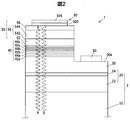
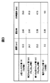
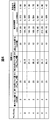
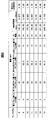
- FIG. 1 is a cross sectional view schematically showing a configuration of a nitride semiconductor light emitting device according to a first embodiment of the present invention. It is a figure which shows roughly the direct emitted light and reflected light which propagate the inside of a light emitting element. It is a figure which shows an example of the film thickness of each layer which comprises the multiple-semiconductor layer of the light emitting element shown in FIG. 1, a refractive index, and optical film thickness. It is a figure which shows the film thickness and light emission output of each layer which comprise the multiple-semiconductor layer of each sample used for experiment of free end reflection.
- FIGS. 1 to 3 A first embodiment of the present invention will be described with reference to FIGS. 1 to 3. Note that the embodiments described below are shown as preferable specific examples for carrying out the present invention, and there are portions that specifically exemplify various technical matters that are technically preferable. The technical scope of the present invention is not limited to this specific embodiment.
- the dimensional ratio of each component in each drawing does not necessarily coincide with the dimensional ratio of the actual nitride semiconductor light emitting device.
- “upper” means a direction from the substrate 10 (see FIG. 1) side to the p-side electrode 92 (see FIG. 1) side described below "" Refers to the direction from the p-side electrode 92 (see FIG.
- “upper” or “lower” indicates the relative positional relationship between one object and another object, and the one object is directly above or other than the other object. Not only those located on the lower side, but also those in which the one object is disposed on the upper side or the lower side indirectly to the other object via another third object.
- FIG. 1 is a cross sectional view schematically showing a configuration of a nitride semiconductor light emitting device according to a first embodiment of the present invention.
- the nitride semiconductor light emitting element 1 (hereinafter, also simply referred to as “light emitting element 1”) is a light emitting diode (Light Emitting Diode: LED) that emits light of a wavelength in the ultraviolet region.
- LED Light Emitting Diode
- the light emitting element 1 which emits deep ultraviolet light having a central wavelength of 250 nm to 350 nm will be described as an example.
- the light emitting device 1 includes a substrate 10, a buffer layer 20, an n-type cladding layer 30, an active layer 40 including multiple quantum well layers, a multiple semiconductor layer 50, and an n-side electrode 90. And the p-side electrode 92.
- the semiconductor constituting the light emitting element 1 includes, for example, a binary system represented by Al x Ga y In 1-x-y N (0 ⁇ x ⁇ 1, 0 ⁇ y ⁇ 1, 0 ⁇ x + y ⁇ 1).
- a ternary or quaternary group III nitride semiconductor can be used. Also, part of these group III elements may be replaced with boron (B), thallium (Tl), etc., and part of N may be phosphorus (P), arsenic (As), antimony (Sb), etc. It may be replaced with bismuth (Bi) or the like.
- the substrate 10 is translucent to deep ultraviolet light emitted by the light emitting element 1.
- the substrate 10 is, for example, a sapphire substrate containing sapphire (Al 2 O 3 ).
- a sapphire (Al 2 O 3 ) substrate for example, an aluminum nitride (AlN) substrate or an aluminum gallium nitride (AlGaN) substrate may be used.
- the buffer layer 20 is formed on the substrate 10.
- the buffer layer 20 includes an AlN layer 22 and an undoped u-Al p Ga 1-p N layer 24 (0 ⁇ p ⁇ 1) formed on the AlN layer 22.
- the substrate 10 and the buffer layer 20 constitute the base structure portion 2.
- the buffer layer 20 may not necessarily be provided.
- the n-type cladding layer 30 is formed on the base structure portion 2.
- the n-type cladding layer 30 is a layer formed of n-type AlGaN (hereinafter, also simply referred to as “n-type AlGaN”), and for example, Al q Ga doped with silicon (Si) as an n-type impurity 1-q N layer (0 ⁇ q ⁇ 1).
- n-type AlGaN n-type AlGaN
- germanium (Ge), selenium (Se), tellurium (Te), carbon (C) or the like may be used as the n-type impurity.
- the n-type cladding layer 30 has a film thickness of about 1 ⁇ m to 3 ⁇ m, and has a film thickness of about 2 ⁇ m, for example.
- the n-type cladding layer 30 may be a single layer or a multilayer structure.
- An active layer 40 including multiple quantum well layers is formed on the n-type cladding layer 30.
- Active layer 40 the barrier of three layers including Al r Ga 1-r N multiple quantum well layer of n-type cladding layer 30 side of the barrier layer 42a formed by, and described later electron blocking layer 52 side of the barrier layer 42c stacked layers 42a, 42b, 42c and Al s Ga 1-s N 3 layers of well layers 44a formed by, 44b, and 44c (0 ⁇ r ⁇ 1,0 ⁇ s ⁇ 1, r> s) alternately Layer containing multiple quantum well layers.
- the active layer 40 combines electrons and holes (hereinafter also referred to as “carriers”) in the multiple quantum well layer to generate light of a predetermined wavelength traveling in both directions above and below the multiple quantum well layer. .
- the active layer 40 is configured to have a band gap of 3.4 eV or more in order to output deep ultraviolet light having a wavelength of 350 nm or less.
- three barrier layers 42 and three well layers 44 are provided in the active layer 40, but the number is not limited to three and may be two or less, or four or more. .
- the first well layer on the n-type cladding layer 30 side is And the well layer on the multiple semiconductor layer 50 side is the third well layer 44c, and the well layer located between the first well layer 44a and the third well layer 44c is the second well layer 44b.
- the multiple semiconductor layer 50 is formed on the active layer 40.
- the multiple semiconductor layer 50 is a layer of a multiple structure including a plurality of p-type semiconductor layers formed of a p-type semiconductor.
- the multiple semiconductor layer 50 is, for example, a layer of a multiple structure including the electron block layer 52, the p-type cladding layer 54, and the p-type contact layer 56. Each layer will be described later.
- FIG. 2 is a view schematically showing direct emission light and reflection light propagating in the light emitting element.
- the solid arrows in FIG. 2 schematically show light (hereinafter also referred to as “directly emitted light”) traveling downward among the light emitted from the multiple quantum well layer. Further, the broken arrow in FIG. 2 is directed toward the upper part of the light emitted from the multiple quantum well layer, reflected by the metal electrode portion 920 (described later), and traveled again downward (hereinafter referred to as “reflected light” (Also referred to as “.”) Is schematically shown. As shown in FIG.
- the multiple semiconductor layer 50 serves as a path through which the reflected light passes, and during the time when the reflected light returns to the position of the multiple quantum well layer, that is, until it merges with the outgoing light directly. It is a layer that reciprocates the inside.
- the reflected light is an example of the first light.
- Directly emitted light is an example of second light. In the following, for convenience of explanation, not only the light actually reflected by the metal electrode portion 920 but also light traveling toward the upper side before reflection is included in the “reflected light”.
- the electron blocking layer 52 is formed on the active layer 40 side.
- the electron block layer 52 is formed of AlN.
- the electron blocking layer 52 has a film thickness of about 1 nm to 10 nm.
- the electron block layer 52 may include a layer formed of p-type AlGaN (hereinafter, also simply referred to as “p-type AlGaN”).
- the electron block layer 52 is not necessarily limited to the p-type semiconductor layer, and may be an undoped semiconductor layer.
- the electron block layer 52 is an example of a p-type semiconductor layer.
- the p-type cladding layer 54 is formed on the electron block layer 52.
- the p-type cladding layer 54 is a layer formed of p-type AlGaN, and is, for example, an Al t Ga 1-t N layer (0 ⁇ t ⁇ 1) doped with magnesium (Mg) as a p-type impurity.
- Mg magnesium
- zinc (Zn), beryllium (Be), calcium (Ca), strontium (Sr), barium (Ba) or the like may be used as the p-type impurity.
- the p-type cladding layer 54 is an example of a p-type semiconductor layer.
- the p-type cladding layer 54 includes two p-type cladding layers respectively formed of two types of p-type AlGaN having different AlN mole fractions (hereinafter also referred to as “Al composition ratio”).
- Al composition ratio p-type cladding layer 54 is positioned on the electron blocking layer 52 side, is formed by p-type having a first Al composition ratio u Al u Ga 1-u N (0 ⁇ u ⁇ 1) First p-type cladding layer 542 and p-type Al v Ga 1-v N (0 ⁇ v ⁇ 1) having a second Al composition ratio v located on the p-type contact layer 56 side And the second p-type cladding layer 544 being formed.
- the second Al composition ratio v is smaller than the first Al composition ratio u. That is, they have a relationship of v ⁇ u. More preferably, the first Al composition ratio u is, for example, about 0.80 (that is, Al 0.8 Ga 0.2 N), and the second Al composition ratio v is, for example, about 0.50 (that is, , Al 0.5 Ga 0.5 N).
- the second Al composition ratio v may be a composition gradient layer which gradually decreases from the p - type Al u Ga 1 -u N layer side having the first Al composition ratio u toward the p-type contact layer 56 side. .
- the p-type cladding layer 54 is not limited to a multilayer structure, and may be a single layer.
- the p-type contact layer 56 is formed on the p-type cladding layer 54.
- the p-type contact layer 56 is, for example, a p-type GaN (hereinafter also referred to as “p-GaN”) layer in which an impurity such as Mg is heavily doped.
- p-GaN p-type GaN
- the p-type contact layer 56 is an example of a p-type semiconductor layer.
- the n-side electrode 90 is formed on a partial region of the n-type cladding layer 30.
- the n-side electrode 90 is formed of, for example, a multilayer film in which titanium (Ti) / aluminum (Al) / Ti / gold (Au) is sequentially stacked on the n-type cladding layer 30 in order.
- the p-side electrode 92 is formed on the p-type contact layer 56.
- the p-side electrode 92 includes a metal electrode portion 920 made of metal and a pad electrode portion 926 formed on the metal electrode portion 920 at the p-type contact layer 56 side.
- metal electrode portion 920 is formed of aluminum (Al).
- the metal electrode portion 920 is Al
- a metal layer such as Ti (titanium), Ni (nickel), Pd (palladium) or the like having a thickness of about 5 nm or less is provided between the p-type contact layer and the Al electrode.
- the metal layer may be inserted, and the adhesion between the p-type contact layer and the metal electrode can be enhanced without substantially reducing the reflectance to deep ultraviolet light.
- FIG. 3 is a view showing an example of the film thickness, the refractive index and the optical film thickness of each layer constituting the multiple semiconductor layer 50 of the light emitting element 1 shown in FIG.
- the optical film thickness is an example of the optical distance of the film thickness.
- the optical film thickness (nm) is a value calculated by multiplying the film thickness (nm) by the refractive index.
- the refractive index showed the value with respect to the light which has a wavelength of 280 nm as an example.
- film thickness when the actual film thickness (nm) is indicated in distinction from the "optical film thickness", it is simply described as "film thickness".
- the optical film thicknesses of the electron block layer 52, the first p-type cladding layer 542, the second p-type cladding layer 544 and the p-type contact layer 56 for 280 nm are 4.6 nm
- the film thickness of each layer can be appropriately adjusted to be 47.6 nm, 61.8 nm and 26.0 nm.
- the film thickness of the multiple semiconductor layer 50 (hereinafter, also referred to as “total optical film thickness”) is 140.0 nm (26.0 nm + 61.8 nm + 47.6 nm + 4.6 nm). This value corresponds to 0.5 times the wavelength of 280 nm.
- samples No. 1 to No. 7 having different total optical film thicknesses, and measured the luminescence intensity (arbitrary unit, our ratio) of each sample. Did.
- the light emitting element in which the p side electrode 92 is not formed was used for seven samples mentioned above for convenience of experiment. Therefore, in such a sample, the reflected light is reflected not at the interface between the metal electrode portion 920 and the p-type contact layer 56 but at the interface between air and the p-type contact layer 56. Since this reflection is performed from a layer having a relatively high refractive index (about 2.60, see FIG. 3) to a layer having a relatively low refractive index (about 1.0), the phase of the reflected light is It is a free end reflection which does not change by reflection. Ultraviolet light having a wavelength of 280 nm was used as the emission wavelength (nm) at which the emission output was measured.
- FIG. 4 is a diagram showing the thicknesses of the electron block layer, the p-type cladding layer and the p-type contact layer in the samples used in the experiment and the light emission output of each sample. As shown in FIG. 4, samples having seven types of total optical film thicknesses were prepared, and the light emission output of each sample was measured. The total optical film thickness shown in FIG. 4 was calculated using the refractive index of each layer shown in FIG.
- the total optical film thickness (nm) is the thickness of the electron block layer 52 (nm) ⁇ 2.30 + the thickness of the first p-type cladding layer 542 (nm) ⁇ 2.38 + the second p-type cladding layer 544
- the thickness is calculated based on the film thickness (nm) ⁇ 2.50 + the film thickness of the p-type contact layer 56 (nm) ⁇ 2.60.
- the multiple semiconductor layer 50 is a path through which only the reflected light does not pass and the reflected light does not pass directly (see FIG. 2). Therefore, the distance that the reflected light travels back and forth in the multiple semiconductor layer 50 in the film thickness direction, that is, the length twice the total optical film thickness is the difference in the path between the reflected light and the directly emitted light (ie, the optical path difference It corresponds to).
- FIG. 5 is a graph showing an example of experimental results showing the relationship between the total optical film thickness and the light emission intensity in free end reflection.
- the horizontal axis in FIG. 5 indicates the total optical film thickness (x ⁇ ), and the vertical axis indicates the light emission output (arbitrary unit).
- Each point in FIG. 5 is a plot of the relationship between the total optical film thickness (x ⁇ ) and the light emission output (arbitrary unit) shown in FIG.
- the broken line in FIG. 5 is a line schematically showing the tendency of change in light emission output (arbitrary unit) with respect to the total optical film thickness (x ⁇ ).
- the light emission output fluctuates so as to repeat the maximum value and the minimum value at predetermined intervals with respect to the total optical film thickness. Specifically, the light emission output fluctuates so as to repeat the maximum value and the minimum value at an interval of about 0.25 (x ⁇ ) with respect to the total optical film thickness. More specifically, the light emission output has a maximum value around about 0.50 (x ⁇ ) and about 1.0 (x ⁇ ) of the total optical film thickness, and the total optical film thickness of about 0.25 (x ⁇ ) and It fluctuates so as to take a local minimum around about 0.75 (x ⁇ ).
- the light emission output periodically fluctuates so as to have a maximum value when the total optical film thickness is an integral multiple of about 0.5 (x ⁇ ).
- the total optical film thickness is an integral multiple of about 0.5 (x ⁇ )
- the reflected light is reflected on the top surface of the p-type contact layer 56 and returns to the third well layer 44c, that is, While merging directly with the outgoing light, it travels back and forth inside the multiple semiconductor layer 50 and travels a distance longer by an integral multiple of the wavelength ⁇ (0.5 ⁇ ⁇ 2) than the direct outgoing light. Therefore, it is considered that the direct emitted light and the reflected light are merged in the same phase and reinforced each other and emitted from the lower side of the multiple quantum well layer.
- the light emission output periodically fluctuates so as to have a local minimum value when the total optical film thickness is an integral multiple of about 0.5 (x ⁇ ) +0.25 (x ⁇ ).
- the total optical film thickness takes a value of an integral multiple of about 0.5 (x ⁇ ) + 0.25 (x ⁇ )
- the reflected light is an integer of the wavelength ⁇ compared to the direct outgoing light before it is merged with the direct outgoing light Go a distance that is twice +0.5 (x ⁇ ) long. Therefore, it is considered that the direct emitted light and the reflected light join in the opposite phase and weaken each other and are emitted from the lower side of the multiple quantum well layer.
- the optical film thickness of the multiple semiconductor layer 50 through which only the reflected light passes corresponds to an integral multiple of the wavelength, it is possible to enhance the light extraction efficiency by enhancing the direct emission light and the reflected light. It was revealed.
- the metal electrode portion 920 and the p-type The light emitting element in which the ITO electrode was further formed between the contact layer 56 was used.
- the reflected light is reflected at the interface between the metal electrode portion 920 and the p-type contact layer 56.
- the refractive index of the metal electrode portion 920 is larger than the refractive index of the p-type contact layer 56. For this reason, the reflection at the metal electrode portion 920 is a fixed end reflection whose phase changes by ⁇ (corresponding to 180 ° and 0.5 wavelength).
- FIG. 6 is a view showing the thicknesses of the electron block layer, the p-type cladding layer and the p-type contact layer in the samples used in the experiment and the light emission output of each sample. As shown in FIG. 6, samples having seven types of total optical film thicknesses were prepared, and the light emission output of each sample was measured. The total optical film thickness shown in FIG. 6 was calculated using the refractive index of each layer shown in FIG.
- FIG. 7 is a graph showing an example of the relationship between the total optical film thickness and the light emission intensity in fixed end reflection.
- Each point in FIG. 7 is a plot of the relationship between the total optical film thickness (x ⁇ ) and the light emission output (arbitrary unit) shown in FIG.
- the light emission output fluctuates so as to repeat the maximum value and the minimum value at predetermined intervals with respect to the total optical film thickness.
- the light emission output fluctuates so as to repeat the maximum value and the minimum value at an interval of about 0.25 (x ⁇ ) with respect to the total optical film thickness.
- the maximum value and the minimum value are present on the side slightly smaller than an integer multiple of 0.25 (x ⁇ ), but this is the case of light traveling obliquely with respect to the metal electrode portion 920 It is an influence, which will be described later.
- the light emission output is obtained when the total optical film thickness is an integral multiple of about 0.5 (x ⁇ ) + 0.25 (x ⁇ ) except for the influence of light traveling obliquely with respect to the metal electrode portion 920. It fluctuates periodically so as to take the maximum value.
- the total optical film thickness takes a value of an integral multiple of about 0.5 (x ⁇ ) + 0.25 (x ⁇ )
- the reflected light is an integer of the wavelength ⁇ compared to the direct outgoing light before it is merged with the direct outgoing light Go a distance that is twice +0.5 (x ⁇ ) long.
- the reflected light changes its phase by 0.5 wavelength at the time of reflection. Therefore, it is considered that the direct emitted light and the reflected light are merged in the same phase and reinforced each other and emitted from the lower side of the multiple quantum well layer.
- the light emission output periodically fluctuates so as to have a local minimum value when the total optical film thickness is an integral multiple of about 0.5 (x ⁇ ).
- the reflected light is an integral multiple of the wavelength ⁇ (0.5 ⁇ x2) than the direct emission light before it is merged with the direct emission light. Go a long distance.
- the reflected light changes its phase by 0.5 wavelength at the time of reflection. Therefore, it is considered that the direct emitted light and the reflected light join in the opposite phase and weaken each other and are emitted from the lower side of the multiple quantum well layer.
- FIG. 8 is a view schematically showing reflected light reflected in an oblique direction with respect to the metal electrode portion 920.
- the third well layer 44 c to the metal electrode portion 920 in the configuration of the light emitting element 1 shown in FIG. 1 are extracted and shown.
- the reflected light which is reflected in the direction (vertical direction in FIG. 8) orthogonal to the metal electrode portion 920 is described as an example, but in the following, for the metal electrode portion 920
- the reflected light that strikes and reflects obliquely is described.
- the alternate long and short dash line in FIG. 8 is an auxiliary line indicating the direction orthogonal to the metal electrode portion 920, and two diagonal broken lines in FIG. 8 indicate the traveling direction of the reflected light. Arrows in FIG. 8 schematically show how reflected light travels inside the multiple semiconductor layer 50.
- Reflected light that is reflected in an oblique direction with respect to the metal electrode portion 920 travels in the multiple semiconductor layer 50 in an oblique direction with respect to the thickness direction of each layer, so the optical path length of the reflected light travels in the thickness direction of each layer It will be longer than the optical path length. Therefore, the light emission output has a maximum value when the total optical film thickness is shorter than the above-mentioned integer multiple of about 0.5 (x ⁇ ) + 0.25 (x ⁇ ).
- the total optical film thickness of the light emission output is Cos ⁇ ° x ( The maximum value is obtained when it is an integral multiple of 0.5 (x ⁇ ) + 0.25 (x ⁇ )). For example, when ⁇ is 20 °, the light emission output has a maximum value when the total optical film thickness is 0.94 ⁇ (an integer multiple of 0.5 (x ⁇ ) + 0.25 (x ⁇ )).
- the total optical film thickness is 0.65 (x ⁇ ) ⁇ 0.15 (x ⁇ ), ie, 0.50 (x ⁇ ) to 0.80 (x ⁇ ).
- the film thickness of the multiple semiconductor layer 50 is 60 nm to 100 nm. If the total optical film thickness is larger than 0.80 (x ⁇ ), the electric resistance increases due to the increase in the film thickness of the layer formed of p-type AlGaN, even if the light emission output falls under the condition that the local maximum value can be obtained. The reason is that the light emission output may be reduced. Also, if the total optical film thickness is smaller than 0.50 (x ⁇ ), it may be considered that the formation of the multiple semiconductor layer 50 from the electron block layer 52 to the p-type contact layer 56 may not be easy. is there.
- the reflected light is, for example, the multiple semiconductor layer 50 including the electron block layer 52, the p-type cladding layer 54 and the p-type contact layer 56.
- the film thickness of the multiple semiconductor layer 50 is determined so as to join directly in the same phase as the outgoing light and emit from the lower side of the multiple quantum well layer while reciprocating inside the device. As a result, the direct emission light and the reflection light strengthen each other, and the light extraction efficiency of the deep ultraviolet light of the light emitting element 1 can be improved.
- the light emitted from the 3rd well layer 44c was mentioned as the example, it may be the light generated from the 1st well layer 44a or the 2nd well layer 44b.
- the interface between any of the well layers 44a, 44b and 44c among the light emitting well layers and the adjacent layer, that is, the upper surface of the well layer 44a, 44b and 44c, to the metal electrode portion 920 The film thickness of each layer may be determined such that the optical distance is Cos ⁇ ° x (an integer multiple of 0.5 (x ⁇ ) + 0.25 (x ⁇ )).
- FIG. 9 is a longitudinal sectional view schematically showing a configuration of a light emitting device 1 according to a second embodiment of the present invention.
- the light emitting element 1 according to the second embodiment of the present invention is different from the light emitting element 1 according to the first embodiment in that a tunnel junction is provided.
- the same components as those in the first embodiment are given the same reference numerals, and redundant description will be omitted, and points different from the first embodiment will be mainly described.
- the light emitting element 1 forms a tunnel junction on the p-type cladding layer 54, instead of the p-type contact layer 56, with a layer containing an n-type semiconductor and a layer containing a p-type semiconductor.
- a tunnel junction 58 is provided.
- the tunnel junction 58 is, for example, a p-type layer 582 formed of a p-type semiconductor such as p-GaN, and an n-type semiconductor such as n-type GaN (hereinafter, also referred to as “n-GaN”).
- n-GaN n-type GaN
- the p-side electrode 92 is provided between the metal electrode portion 920 and the tunnel junction 58 in addition to the metal electrode portion 920, and is located on the tunnel junction 58 side and includes indium tin oxide (ITO). And further includes a Ti electrode portion 924 positioned between the metal electrode portion 920 and the ITO contact electrode portion 922.
- the Ti electrode portion 924 improves adhesion with the metal electrode portion 920 and the ITO contact electrode portion 922, and suppresses corrosion and peeling that may occur between the metal electrode portion 920 and the ITO contact electrode portion 922.
- the Ti electrode portion 924 preferably has a film thickness of about 5 nm or less. By thickening the film thickness of the Ti electrode part 924, it is for suppressing that the reflectance by the metal electrode part 920 falls. Note that, instead of the Ti electrode portion 924, an electrode portion containing Ni or Pd may be used.
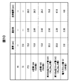
- FIG. 10 is a view showing an example of the film thickness, the refractive index and the optical film thickness of each layer constituting the multiple semiconductor layer 50 of the light emitting element 1 shown in FIG.
- the electron block layer 52, the first p-type cladding layer 542, the second p-type cladding layer 544, the p-type layer 582, the n-type layer 584 and the ITO contact electrode portion 922 for 280 nm.
- the film thicknesses of the respective layers can be appropriately adjusted so that the optical film thickness of the respective layers becomes 4.6 nm, 47.6 nm, 75.8 nm, 26.0 nm, 26.0 nm and 30.0 nm, respectively.
- the total optical film thickness of the layer between the multiple quantum well layer and the metal electrode portion 920 is 210.0 nm (30.0 nm + 26.0 nm + 26.0 nm + 75.8 nm + 47.6 nm + 4.6 nm). This value corresponds to 0.75 times the wavelength 280 nm.
- a multiple quantum well layer including a plurality of well layers (44) for coupling carriers to generate light, and the light generated from the multiple quantum well layer located above the multiple quantum well layer Among them, a plurality of metal electrodes (920) reflecting the first light traveling upward, a plurality of p-type semiconductors located between the multiple quantum well layer and the metal electrodes (920)
- the nitride semiconductor light emitting device (1) There has a thickness of emitted at the lower side of the multiple quantum well layer are merged in the same phase, the nitride semiconductor light emitting device (1).
- the optical distance of the film thickness of the multiple semiconductor layer (50) is substantially equal to a value obtained by adding 0.25 times the wavelength to an integral multiple of 0.5 of the wavelength of the first light.
- the optical distance of the film thickness of the multiple semiconductor layer (50) is given by the following equation, where an angle between the thickness direction of the multiple semiconductor layer (50) and the first light is ⁇ °: The nitride semiconductor light emitting device (1) according to the above [2], which is substantially equal to a value obtained by adding 0.25 times the wavelength to an integral multiple of 0.5 of the light wavelength of 1 and multiplying Cos ⁇ °.
- the optical distance from the top surface of any of the plurality of well layers (44) constituting the multiple quantum well layer to the interface between the multiple semiconductor layer (50) and the metal electrode portion (920) is The nitride semiconductor light emitting device according to any one of [1] to [4], which is substantially equal to a value obtained by adding 0.25 times the wavelength to an integral multiple of 0.5 of the wavelength of the first light. (1).
- the optical distance from the top surface of any of the plurality of well layers (44) constituting the multiple quantum well layer to the interface between the multiple semiconductor layer (50) and the metal electrode portion (920) is The nitride semiconductor light emitting device (1) according to the above [6], wherein the value is obtained by multiplying the integral multiple of 0.5 of the wavelength of the first light by 0.25 times the wavelength and multiplying the value by Cos ⁇ ° ).
- the multiple semiconductor layer (50) is formed of p-type AlGaN located on the electron block layer (52) located on the multiple quantum well layer side and the electron block layer (52)
- the nitride semiconductor light emitting device (1) according to any one of the above [1] to [4], which is configured to include a p-type cladding layer (54).
- the multiple semiconductor layer (50) further includes a p-type contact layer (56) formed of p-type GaN, located on the p-type cladding layer (54), from [1] to [1]
- the nitride semiconductor light emitting device (1) according to any one of [4].
- the p-type cladding layer (54) is a first p-type cladding layer (542) formed of p-type AlGaN having a first composition ratio, located on the electron block layer (52) side. And a second p-type cladding layer (544) formed of p-type AlGaN located on the p-type contact layer (56) side and having a second composition ratio smaller than the first composition ratio.
- the tunnel junction (58) includes a p-type layer (582) formed of a p-type semiconductor and an n-type layer (584) formed of an n-type semiconductor.
- the nitride semiconductor light emitting element as described in (1).
- the nitride semiconductor light emitting device (1) according to any one of [1] to [4], wherein the metal electrode portion (920) is formed of Al.
- An ITO contact electrode portion provided between the metal electrode portion (920) and the tunnel junction (58) and including indium tin oxide located on the tunnel junction (58) side
- Light emitting element (1)
- An ITO contact electrode portion provided between the metal electrode portion (920) and the tunnel junction (58) and including indium tin oxide and located on the tunnel junction (58) side
Landscapes
- Led Devices (AREA)
Abstract
窒化物半導体発光素子は、多重量子井戸層と、上方に進む第1の光を反射する金属電極部と、多重量子井戸層と金属電極部との間に位置して、複数のp型半導体層を含む多重半導体層であって、第1の光が金属電極部と多重半導体層との界面で反射して下方に向かって進む第2の光と合流するまでの間に内部を往復する多重半導体層とを備え、多重半導体層は、多重半導体層の内部を往復した第1の光と、第2の光とを同位相で合流させて多重量子井戸層の下方側から出射する膜厚を有する。
Description
本発明は、窒化物半導体発光素子に関する。
近年、紫外光を出力する発光ダイオードやレーザダイオード等の窒化物半導体発光素子が提供されており、発光強度を向上させた窒化物半導体発光素子の開発が進められている(特許文献1参照。)。
特許文献1に記載の半導体発光素子は、第1の導電型を有する第1の半導体層と、前記第1の半導体層上に形成された発光層と、前記発光層上に形成された第2の導電型を有する第2の半導体層と、前記第2の半導体層上に形成され、前記第2の半導体層よりも低い光屈折率を有する透光性の導電体層と、前記導電体層上に形成された金属層とを含み、前記第2の半導体層の層厚は、前記発光層からの直接放出光及び前記導電体層からの導電体層反射光の位相が、前記発光層から前記第1の半導体層の方向に向かって進む際に整合するように定められ、前記導電体層の層厚は、前記導電体層反射光及び前記金属層からの金属層反射光の位相が、前記発光層から前記第1の半導体層の方向に向かって進む際に整合するように定められている構成を有する。
このように、特許文献1に記載の半導体発光素子では、直接放出光及び導電体層反射光の位相と、導電体層反射光及び金属層反射光の位相とがそれぞれ整合するように、第2の半導体層の層厚及び導電体層の層厚をそれぞれ個別に定めることにより、光の取出し効率を向上させている。
ところで、特許文献1に記載の半導体発光素子では、第2の半導体層にp型GaN層が用いられている。しかしながら、p型GaN層は、深紫外光を吸収する性質を有する。そのため、深紫外線を発光する深紫外線発光素子では、第2の半導体層の層厚及び導電体層の層厚をそれぞれ個別に定める対策を施してもなお、光の取出し効率が十分に得られない可能性がある。
そこで、本発明の目的は、深紫外光の取出し効率を向上させることができる窒化物半導体発光素子を提供することにある。
本発明の一実施形態による窒化物半導体発光素子は、キャリアを結合させて光を発生させる複数の井戸層を含む多重量子井戸層と、前記多重量子井戸層の上方に位置して、前記多重量子井戸層から発生した前記光のうち上方に進む第1の光を反射する金属電極部と、前記多重量子井戸層と前記金属電極部との間に位置して、p型の半導体により形成されている複数のp型半導体層を含む多重半導体層であって、前記第1の光が前記金属電極部と前記多重半導体層との界面で反射して前記多重井戸層から発せられた光のうち下方に向かって進む第2の光と合流するまでの間に内部を往復する多重半導体層とを備え、前記多重半導体層は、前記多重半導体層の内部を往復した前記第1の光と、前記第2の光とが同位相で合流させて前記多重量子井戸層の下方側から出射する膜厚を有する。
本発明の一実施態様によれば、深紫外光の取出し効率を向上させることができる窒化物半導体発光素子を提供することができる。
[第1の実施の形態]
本発明の第1の実施の形態について、図1から図3を参照して説明する。なお、以下に説明する実施の形態は、本発明を実施する上での好適な具体例として示すものであり、技術的に好ましい種々の技術的事項を具体的に例示している部分もあるが、本発明の技術的範囲は、この具体的態様に限定されるものではない。また、各図面における各構成要素の寸法比は、必ずしも実際の窒化物半導体発光素子の寸法比と一致するものではない。なお、以下、本発明の実施の形態を説明するにあたり、「上方」とは、後述する基板10(図1参照)側からp側電極92(図1参照)側に向かう方向をいい、「下方」とは、p側電極92(図1参照)側から基板10(図1参照)側に向かう方向をいう。また、「上方」又は「下方」は、一つの対象物と他の対象物との相対的な位置関係を示すものであり、当該一つの対象物が当該他の対象物に直接的に上側又は下側に配置されているもののみならず、当該一つの対象物が別の第三対象物を介して当該他の対象物に間接的に上側又は下側に配置されているものも含む。
本発明の第1の実施の形態について、図1から図3を参照して説明する。なお、以下に説明する実施の形態は、本発明を実施する上での好適な具体例として示すものであり、技術的に好ましい種々の技術的事項を具体的に例示している部分もあるが、本発明の技術的範囲は、この具体的態様に限定されるものではない。また、各図面における各構成要素の寸法比は、必ずしも実際の窒化物半導体発光素子の寸法比と一致するものではない。なお、以下、本発明の実施の形態を説明するにあたり、「上方」とは、後述する基板10(図1参照)側からp側電極92(図1参照)側に向かう方向をいい、「下方」とは、p側電極92(図1参照)側から基板10(図1参照)側に向かう方向をいう。また、「上方」又は「下方」は、一つの対象物と他の対象物との相対的な位置関係を示すものであり、当該一つの対象物が当該他の対象物に直接的に上側又は下側に配置されているもののみならず、当該一つの対象物が別の第三対象物を介して当該他の対象物に間接的に上側又は下側に配置されているものも含む。
図1は、本発明の第1の実施の形態に係る窒化物半導体発光素子の構成を概略的に示す断面図である。窒化物半導体発光素子1(以下、単に「発光素子1」ともいう。)は、紫外領域の波長の光を発する発光ダイオード(Light Emitting Diode:LED)である。本実施の形態では、特に、中心波長が250nm~350nmの深紫外光を発する発光素子1を例に挙げて説明する。
図1に示すように、発光素子1は、基板10と、バッファ層20と、n型クラッド層30と、多重量子井戸層を含む活性層40と、多重半導体層50と、n側電極90と、p側電極92とを含んで構成されている。
発光素子1を構成する半導体には、例えば、AlxGayIn1-x-yN(0≦x≦1、0≦y≦1、0≦x+y≦1)にて表される2元系、3元系若しくは4元系のIII族窒化物半導体を用いることができる。また、これらのIII族元素の一部は、ホウ素(B)、タリウム(Tl)等で置き換えても良く、また、Nの一部をリン(P)、ヒ素(As)、アンチモン(Sb)、ビスマス(Bi)等で置き換えても良い。
基板10は、発光素子1が発する深紫外光に対して透光性を有している。基板10は、例えば、サファイア(Al2O3)を含むサファイア基板である。基板10には、サファイア(Al2O3)基板の他に、例えば、窒化アルミニウム(AlN)基板や、窒化アルミニウムガリウム(AlGaN)基板を用いてもよい。
バッファ層20は、基板10上に形成されている。バッファ層20は、AlN層22と、AlN層22上に形成されるアンドープのu-AlpGa1-pN層24(0≦p≦1)を含んで構成されている。また、基板10及びバッファ層20は、下地構造部2を構成する。なお、基板10がAlN基板またはAlGaN基板である場合、バッファ層20は必ずしも設けなくてもよい。
n型クラッド層30は、下地構造部2上に形成されている。n型クラッド層30は、n型のAlGaN(以下、単に「n型AlGaN」ともいう。)により形成された層であり、例えば、n型の不純物としてシリコン(Si)がドープされたAlqGa1-qN層(0≦q≦1)である。なお、n型の不純物としては、ゲルマニウム(Ge)、セレン(Se)、テルル(Te)、炭素(C)等を用いてもよい。n型クラッド層30は、1μm~3μm程度の膜厚を有し、例えば、2μm程度の膜厚を有している。n型クラッド層30は、単層でもよく、多層構造でもよい。
多重量子井戸層を含む活性層40は、n型クラッド層30上に形成されている。活性層40は、AlrGa1-rNによって形成された多重量子井戸層のn型クラッド層30側の障壁層42a、及び後述する電子ブロック層52側の障壁層42cを含む3層の障壁層42a,42b,42cとAlsGa1-sNによって形成された3層の井戸層44a,44b,44c(0≦r≦1、0≦s≦1、r>s)とを交互に積層した多重量子井戸層を含む層である。
活性層40は、多重量子井戸層内で電子及びホール(以下、「キャリア」ともいう。)を結合させて、多重量子井戸層の上方及び下方の双方向に進む所定の波長の光を発生させる。活性層40は、波長350nm以下の深紫外光を出力するためにバンドギャップが3.4eV以上となるように構成されている。なお、本実施の形態では、活性層40に障壁層42及び井戸層44を各3層ずつ設けたが、必ずしも3層に限定されるものではなく、2層以下でもよく、4層以上でもよい。また、以下では、3つの井戸層44a,44b,44cのうちのいずれかの井戸層を他の井戸層と区別して特定する必要がある場合は、n型クラッド層30側の井戸層を第1の井戸層44aとし、多重半導体層50側の井戸層を第3の井戸層44cとし、第1の井戸層44a及び第3の井戸層44cの間に位置する井戸層を第2の井戸層44bとして説明する。
多重半導体層50は、活性層40上に形成されている。多重半導体層50は、p型の半導体により形成されている複数のp型半導体層を含む多重構造の層である。具体的には、多重半導体層50は、例えば、電子ブロック層52と、p型クラッド層54と、p型コンタクト層56とを含む多重構造の層である。各層については、後述する。
図2は、発光素子内を伝播する直接出射光及び反射光を概略的に示す図である。図2の実線の矢印は、多重量子井戸層から発せられる光のうち下方に向かって進む光(以下、「直接出射光」ともいう。)を模式的に示したものである。また、図2の破線の矢印は、多重量子井戸層から発せられる光のうち上方に向かって進み、金属電極部920(後述)で反射して再び下方に向って進む光(以下、「反射光」ともいう。)を模式的に示したものである。図2に示すように、多重半導体層50は、反射光が通過する経路となるとともに、反射光が多重量子井戸層の位置に戻るまでの間、すなわち、直接出射光と合流するまでの間に内部を往復する層である。なお、反射光は、第1の光の一例である。直接出射光は、第2の光の一例である。また、以下では、説明の便宜上、金属電極部920で実際に反射した光のみならず、反射する前の上方に向かって進む光も「反射光」に含めて説明する。
電子ブロック層52は、活性層40側に形成されている。電子ブロック層52は、AlNにより形成されている。電子ブロック層52は、1nm~10nm程度の膜厚を有している。なお、電子ブロック層52は、p型のAlGaN(以下、単に「p型AlGaN」ともいう。)により形成された層を含んでもよい。また、電子ブロック層52は、必ずしもp型の半導体層に限られず、アンドープの半導体層でもよい。電子ブロック層52は、p型半導体層の一例である。
p型クラッド層54は、電子ブロック層52上に形成されている。p型クラッド層54は、p型AlGaNにより形成される層であり、例えば、p型の不純物としてマグネシウム(Mg)がドープされたAltGa1-tN層(0≦t≦1)である。なお、p型の不純物としては、亜鉛(Zn)、ベリリウム(Be)、カルシウム(Ca)、ストロンチウム(Sr)、バリウム(Ba)等を用いてもよい。p型クラッド層54は、p型半導体層の一例である。
好ましくは、p型クラッド層54は、AlNモル分率(以下、「Al組成比」ともいう。)の異なる2種類のp型AlGaNによりそれぞれ形成された2つのp型クラッド層を備える。具体的には、p型クラッド層54は、電子ブロック層52側に位置して、第1のAl組成比uを有するp型AluGa1-uN(0<u≦1)により形成されている第1のp型クラッド層542と、p型コンタクト層56側に位置して、第2のAl組成比vを有するp型AlvGa1-vN(0<v≦1)により形成されている第2のp型クラッド層544とを含んで構成されている。
好ましくは、第2のAl組成比vは、第1のAl組成比uよりも小さい。すなわち、v<uの関係を有する。より好ましくは、第1のAl組成比uは、例えば、約0.80(すなわち、Al0.8Ga0.2N)、第2のAl組成比vは、例えば、約0.50(すなわち、Al0.5Ga0.5N)である。また、第2のAl組成比vは、第1のAl組成比uを有するp型AluGa1-uN層側からp型コンタクト層56側に向かって徐々に小さくなる組成傾斜層でもよい。なお、p型クラッド層54は、多層構造に限られるものではなく、単層でもよい。
p型コンタクト層56は、p型クラッド層54上に形成されている。p型コンタクト層56は、例えば、Mg等の不純物が高濃度にドープされたp型のGaN(以下、「p-GaN」ともいう。)層である。p型コンタクト層56は、p型半導体層の一例である。
n側電極90は、n型クラッド層30の一部の領域上に形成されている。n側電極90は、例えば、n型クラッド層30の上に順にチタン(Ti)/アルミニウム(Al)/Ti/金(Au)が順に積層された多層膜で形成される。
p側電極92は、p型コンタクト層56の上に形成されている。p側電極92は、p型コンタクト層56側に位置して、金属により形成された金属電極部920と、金属電極部920上に形成されたパッド電極部926とを含んで構成されている。金属電極部920を形成する金属材料には、例えば、アルミニウム(Al)、金(Au)、銀(Ag)、ニッケル(Ni)等を用いることができる。好ましくは、金属電極部920は、アルミニウム(Al)により形成される。金属電極部920の材料にAlを用いることにより、深紫外光に対する反射率を向上させることができるからである。なお、深紫外線に対するAlの反射率は、約90%程度である。また、金属電極部920がAlである場合には、p型コンタクト層とAl電極の間に厚さが5nm程度以下のTi(チタン)、Ni(ニッケル)、Pd(パラジウム)等の金属層を挿入してもよく、この金属層の挿入により、深紫外線に対する反射率をほとんど下げることなく、p型コンタクト層と金属電極の密着性を高めることができる。
図3は、図1に示す発光素子1の多重半導体層50を構成する各層の膜厚、屈折率及び光学膜厚の一例を示す図である。光学膜厚は、膜厚の光学的距離の一例である。なお、光学膜厚(nm)は、膜厚(nm)に屈折率を乗じて算出した値である。また、屈折率は、一例として、280nmの波長を有する光に対する値を示した。以下の説明において、「光学膜厚」と区別して、実際の膜厚(nm)を示すときは、単に「膜厚」と記載する。
図3に示すように、一例として、280nmに対する電子ブロック層52、第1のp型クラッド層542、第2のp型クラッド層544及びp型コンタクト層56の光学膜厚がそれぞれ4.6nm、47.6nm、61.8nm及び26.0nmになるように、各層の膜厚を適宜調整することができる。この場合、多重半導体層50の膜厚(以下、「総光学膜厚」ともいう。)は、140.0nm(26.0nm+61.8nm+47.6nm+4.6nm)である。この値は、波長280nmの0.5倍に相当している。
(自由端反射における総光学膜厚と発光強度との関係を調べる実験)
次に、図4及び図5を参照して、総光学膜厚と発光強度との関係を説明する。以下では、フリップ型のサンプル、すなわち、基板10側から光を取り出すタイプのサンプルを例に挙げて説明する。本発明者らは、直接出射光と、反射光との位相差、及びこれら直接出射光と反射光との強め合いの関係を評価することを目的として、総光学膜厚、すなわち、多重半導体層50の光学膜厚と発光強度との関係を調べる実験を行った。
次に、図4及び図5を参照して、総光学膜厚と発光強度との関係を説明する。以下では、フリップ型のサンプル、すなわち、基板10側から光を取り出すタイプのサンプルを例に挙げて説明する。本発明者らは、直接出射光と、反射光との位相差、及びこれら直接出射光と反射光との強め合いの関係を評価することを目的として、総光学膜厚、すなわち、多重半導体層50の光学膜厚と発光強度との関係を調べる実験を行った。
具体的には、発明者らは、総光学膜厚の異なる7個のサンプル(サンプルNo.1~No.7)を作製し、各サンプルの発光強度(任意単位、当社比)を測定する実験を行った。
なお、実験の便宜上、上述した7個のサンプルには、p側電極92が形成されていない発光素子を用いた。このため、このようなサンプルでは、反射光は、金属電極部920とp型コンタクト層56との界面ではなく、空気とp型コンタクト層56との界面で反射する。この反射は、屈折率が相対的に高い層(約2.60、図3参照)から屈折率が相対的に低い層(約1.0)に当たって行われる反射であるため、反射光の位相が反射によって変化しない自由端反射である。発光出力を計測する発光波長(nm)には、280nmの波長を有する紫外線を用いた。
図4は、実験に用いたサンプルにおける電子ブロック層、p型クラッド層及びp型コンタクト層の膜厚及び各サンプルの発光出力を示す図である。図4に示すように、7種類の総光学膜厚を有するサンプルを用意し、各サンプルの発光出力を測定した。なお、図4に示す総光学膜厚は、図3に示した各層の屈折率を用いて算出した。すなわち、総光学膜厚(nm)は、電子ブロック層52の膜厚(nm)x2.30+第1のp型クラッド層542の膜厚(nm)x2.38+第2のp型クラッド層544の膜厚(nm)x2.50+p型コンタクト層56の膜厚(nm)x2.60に基づいて算出した。また、図4の「総光学膜厚(xλ=280nm)」の欄には、各サンプルにおける測定波長(280nm)に対する総光学膜厚(nm)の比率を示した。
以下、発光は、3つの井戸層44のうち電子ブロック層52側の第3の井戸層44cで行われるものとして説明する。多重半導体層50は、直接出射光は通らず、反射光のみが通る経路である(図2参照)。したがって、反射光が多重半導体層50の内部を膜厚方向に往復する距離、すなわち、総光学膜厚の2倍の長さは、反射光と直接出射光との経路の差(すなわち、光路差)に相当する。
図5は、自由端反射における総光学膜厚と発光強度合との関係を示す実験結果の一例を示すグラフである。図5の横軸は、総光学膜厚(xλ)を示し、縦軸は、発光出力(任意単位)を示している。図5の各点は、図4に示した総光学膜厚(xλ)及び発光出力(任意単位)の関係をプロットしたものである。図5の破線は、総光学膜厚(xλ)に対する発光出力(任意単位)の変化の傾向を概略的に示す線である。
図5に示すように、発光出力は、総光学膜厚に対して所定の間隔で極大値と極小値とを繰り返すように変動している。具体的には、発光出力は、総光学膜厚に対して約0.25(xλ)の間隔で極大値と極小値とを繰り返すように変動している。より具体的には、発光出力は、総光学膜厚が約0.50(xλ)及び約1.0(xλ)付近で極大値をとり、総光学膜厚が約0.25(xλ)及び約0.75(xλ)付近で極小値をとるように変動している。
このように、発光出力は、総光学膜厚が約0.5(xλ)の整数倍のときに極大値をとるように周期的に変動している。総光学膜厚が約0.5(xλ)の整数倍の値をとる場合、反射光は、p型コンタクト層56の上面で反射して第3の井戸層44cに戻るまでの間、すなわち、直接出射光と合流するまでの間に、多重半導体層50の内部を往復し直接出射光よりも波長λ(0.5λx2)の整数倍長い距離を進む。そのため、直接出射光と反射光とが同位相で合流して互いに強め合って多重量子井戸層の下方側から出射したと考えられる。
一方で、発光出力は、総光学膜厚が約0.5(xλ)の整数倍+0.25(xλ)のときに極小値をとるように周期的に変動している。総光学膜厚が約0.5(xλ)の整数倍+0.25(xλ)の値をとる場合、反射光は、直接出射光と合流するまでの間に直接出射光よりも波長λの整数倍+0.5(xλ)長い距離を進む。そのため、直接出射光と反射光とが逆位相で合流して互いに弱め合って多重量子井戸層の下方側から出射したと考えられる。
以上のように、反射光のみが通る多重半導体層50の光学膜厚が波長の整倍数に相当するときに、直接出射光と反射光とが強め合い光の取出し効率を向上させることができることが明らかになった。
(固定端反射における総光学膜厚と発光強度との関係)
次に、図6及び図7を参照して、他のサンプルにおける総光学膜厚と発光出力との関係を説明する。本発明者らは、上述の自由端反射の実験に加えて、固定端反射における直接出射光と、反射光との位相差、及びこれら直接出射光と反射光との強め合いの関係を評価することを目的として、総光学膜厚の異なる7個のサンプル(サンプルNo.8~No.14)を作製し、各サンプルの発光強度(任意単位、当社比)を測定する実験を行った。
以下、自由端反射の実験と同様に、フリップ型のサンプルを例に挙げて説明する。また、上述したように、総光学膜厚の2倍の長さは、反射光と直接出射光との経路の差(すなわち、光路差)に相当する。
次に、図6及び図7を参照して、他のサンプルにおける総光学膜厚と発光出力との関係を説明する。本発明者らは、上述の自由端反射の実験に加えて、固定端反射における直接出射光と、反射光との位相差、及びこれら直接出射光と反射光との強め合いの関係を評価することを目的として、総光学膜厚の異なる7個のサンプル(サンプルNo.8~No.14)を作製し、各サンプルの発光強度(任意単位、当社比)を測定する実験を行った。
以下、自由端反射の実験と同様に、フリップ型のサンプルを例に挙げて説明する。また、上述したように、総光学膜厚の2倍の長さは、反射光と直接出射光との経路の差(すなわち、光路差)に相当する。
なお、実験の便宜上、上述した7個のサンプル(サンプルNo.8~No.14)には、上述した本発明の第1の実施の形態に係る発光素子1において、金属電極部920とp型コンタクト層56との間にITO電極がさらに形成されている発光素子を用いた。このようなサンプルでは、反射光は、金属電極部920とp型コンタクト層56との界面で反射する。金属電極部920の屈折率は、p型コンタクト層56の屈折率よりも大きい。このため、金属電極部920での反射は、位相がπ(180°、0.5波長に相当)変化する固定端反射である。
図6は、実験に用いたサンプルにおける電子ブロック層、p型クラッド層及びp型コンタクト層の膜厚及び各サンプルの発光出力を示す図である。図6に示すように、7種類の総光学膜厚を有するサンプルを用意し、各サンプルの発光出力を測定した。なお、図6に示す総光学膜厚は、図3に示した各層の屈折率を用いて算出した。
図7は、固定端反射における総光学膜厚と発光強度との関係の一例を示すグラフである。図7の各点は、図6に示した総光学膜厚(xλ)及び発光出力(任意単位)の関係をプロットしたものである。図7に示すように、発光出力は、総光学膜厚に対して所定の間隔で極大値と極小値とを繰り返すように変動している。具体的には、発光出力は、総光学膜厚に対して約0.25(xλ)の間隔で極大値と極小値とを繰り返すように変動している。実際には図7では、極大値および極小値は、0.25(xλ)の整数倍よりわずかに小さい側に存在しているが、これは金属電極部920に対して斜め方向に進む光の影響であり、それについては後述する。
このように、発光出力は、金属電極部920に対して斜め方向に進む光の影響を除けば、総光学膜厚が約0.5(xλ)の整数倍+0.25(xλ)のときに極大値をとるように周期的に変動している。総光学膜厚が約0.5(xλ)の整数倍+0.25(xλ)の値をとる場合、反射光は、直接出射光と合流するまでの間に直接出射光よりも波長λの整数倍+0.5(xλ)長い距離を進む。また、上述のように、反射光は反射の際に位相が0.5波長分変化する。そのため、直接出射光と反射光とが同位相で合流して互いに強め合って多重量子井戸層の下方側から出射したと考えられる。
一方で、発光出力は、総光学膜厚が約0.5(xλ)の整数倍のときに極小値をとるように周期的に変動している。総光学膜厚が約0.5(xλ)の整数倍の値をとる場合、反射光は、直接出射光と合流するまでの間に直接出射光よりも波長λ(0.5λx2)の整数倍長い距離を進む。また、上述のように、反射光は反射の際に位相が0.5波長分変化する。そのため、直接出射光と反射光とが逆位相で合流して互いに弱め合って多重量子井戸層の下方側から出射したと考えられる。
以上のように、反射光のみが通る多重半導体層50の光学膜厚が波長の整倍数+所定の値に相当するときに、直接出射光と反射光とが強め合い光の取出し効率を向上させることができることが明らかになった。
図8は、金属電極部920に対して斜め方向に反射する反射光を模式的に示す図である。図8では、図1に示した発光素子1の構成のうち第3の井戸層44cから金属電極部920までを抜き出して示している。上述の例では、説明の便宜上、金属電極部920に対して直行する方向(図8の図示上下方向)に当たって反射する反射光を例に挙げて説明したが、以下では、金属電極部920に対して斜め方向に当たって反射する反射光について説明する。図8の一点鎖線は、金属電極部920に対して直行する方向を示す補助線であり、図8の2つの斜めの破線は、反射光の進む方向をそれぞれ示している。図8内の矢印は、反射光が多重半導体層50の内部を進む様子を模式的に示すものである。
金属電極部920に対して斜め方向に反射する反射光は、多重半導体層50内を、各層の厚み方向に対して斜め方向に進むため、当該反射光の光路長は、各層の厚み方向に進むときの光路長よりも長くなる。そのため、発光出力は、総光学膜厚が上述した約0.5(xλ)の整数倍+0.25(xλ)よりも短いときに極大値となる。
具体的には、図8に示すように、反射光の方向と金属電極部920に対して直行する方向とのなす角をθ°とすると、発光出力は、総光学膜厚がCosθ°x(0.5(xλ)の整数倍+0.25(xλ))のときに極大値となる。例えば、θが20°の場合、発光出力は、総光学膜厚が0.94x(0.5(xλ)の整数倍+0.25(xλ))のときに極大値となる。
好ましくは、総光学膜厚は、0.65(xλ)±0.15(xλ)、すなわち、0.50(xλ)から0.80(xλ)である。換言すれば、多重半導体層50の膜厚は、60nmから100nmである。総光学膜厚が0.80(xλ)よりも大きい場合、発光出力が極大値をとり得る条件にあたるとしても、p型AlGaNにより形成される層の膜厚が大きくなることによって電気抵抗が大きくなり、発光出力が低下する可能性があると考えられるからである。また、総光学膜厚が0.50(xλ)よりも小さい場合、電子ブロック層52からp型コンタクト層56までに亘る多重半導体層50の形成が容易でなくなる可能性があると考えられるからである。
(第1の実施の形態の作用及び効果)
以上説明したように、本発明の第1の実施の形態に係る発光素子1では、反射光が、例えば、電子ブロック層52、p型クラッド層54及びp型コンタクト層56を含む多重半導体層50の内部を往復する間に、直接出射光と同位相で合流して多重量子井戸層の下方側から出射するように多重半導体層50の膜厚が定められている。これにより、直接出射光と反射光とが互いに強め合い、発光素子1の深紫外光の取出し効率を向上させることが可能となる。
以上説明したように、本発明の第1の実施の形態に係る発光素子1では、反射光が、例えば、電子ブロック層52、p型クラッド層54及びp型コンタクト層56を含む多重半導体層50の内部を往復する間に、直接出射光と同位相で合流して多重量子井戸層の下方側から出射するように多重半導体層50の膜厚が定められている。これにより、直接出射光と反射光とが互いに強め合い、発光素子1の深紫外光の取出し効率を向上させることが可能となる。
<変形例>
上述の例では、第3の井戸層44cから発せられた光を例に挙げて説明したが、第1の井戸層44aや第2の井戸層44bから発生された光であってもよい。この場合、発光する井戸層のうちのいずれかの井戸層44a,44b,44cと隣接する層との界面、すなわち、当該いずれかの井戸層44a,44b,44cの上面から金属電極部920までの光学的距離が、Cosθ°x(0.5(xλ)の整数倍+0.25(xλ))になるように各層の膜厚を定めてもよい。
上述の例では、第3の井戸層44cから発せられた光を例に挙げて説明したが、第1の井戸層44aや第2の井戸層44bから発生された光であってもよい。この場合、発光する井戸層のうちのいずれかの井戸層44a,44b,44cと隣接する層との界面、すなわち、当該いずれかの井戸層44a,44b,44cの上面から金属電極部920までの光学的距離が、Cosθ°x(0.5(xλ)の整数倍+0.25(xλ))になるように各層の膜厚を定めてもよい。
[第2の実施の形態]
図9は、本発明の第2の実施の形態に係る発光素子1の構成を概略的に示す縦断面図である。本発明の第2の実施の形態に係る発光素子1は、トンネルジャンクションを備えている点で、第1の実施の形態に係る発光素子1と相違する。以下、第1の実施の形態と同一の構成要素については、同一の符号を付してその重複した説明を省略するとともに、第1の実施の形態と異なる点を中心に説明する。
図9は、本発明の第2の実施の形態に係る発光素子1の構成を概略的に示す縦断面図である。本発明の第2の実施の形態に係る発光素子1は、トンネルジャンクションを備えている点で、第1の実施の形態に係る発光素子1と相違する。以下、第1の実施の形態と同一の構成要素については、同一の符号を付してその重複した説明を省略するとともに、第1の実施の形態と異なる点を中心に説明する。
図9に示すように、発光素子1は、p型クラッド層54上に、p型コンタクト層56に代えて、n型の半導体を含む層とp型の半導体を含む層とをトンネルジャンクション接合するトンネルジャンクション58を備えている。トンネルジャンクション58は、例えば、p-GaN等のp型の半導体により形成されたp型層582と、例えば、n型のGaN(以下、「n-GaN」ともいう。)等のn型の半導体により形成されたn型層584とを含む。
p側電極92は、金属電極部920に加えて、金属電極部920とトンネルジャンクション58との間に設けられ、トンネルジャンクション58側に位置して、酸化インジウムスズ(Indium Tin Oxide:ITO)を含んで構成され、オーミック特性に優れているITOコンタクト電極部922と、金属電極部920及びITOコンタクト電極部922の間に位置するTi電極部924とをさらに備えている。なお、Ti電極部924は、金属電極部920及びITOコンタクト電極部922との密着性を向上し、金属電極部920及びITOコンタクト電極部922の間で生じる可能性のある腐食や剥離を抑制する。また、Ti電極部924は、好ましくは、5nm程度以下の膜厚を有する。Ti電極部924の膜厚を厚くすることによって、金属電極部920による反射率が低下してしまうことを抑制するためである。なお、Ti電極部924に代えて、Ni又はPdを含む電極部を用いてもよい。
図10は、図9に示す発光素子1の多重半導体層50を構成する各層の膜厚、屈折率及び光学膜厚の一例を示す図である。図10に示すように、一例として、280nmに対する電子ブロック層52、第1のp型クラッド層542、第2のp型クラッド層544、p型層582、n型層584及びITOコンタクト電極部922の光学膜厚がそれぞれ4.6nm、47.6nm、75.8nm、26.0nm、26.0nm及び30.0nmになるように、各層の膜厚を適宜調整することができる。この場合、多重量子井戸層及び金属電極部920の間の層の総光学膜厚は、210.0nm(30.0nm+26.0nm+26.0nm+75.8nm+47.6nm+4.6nm)である。この値は、波長280nmの0.75倍に相当している。
(第2の実施の形態の作用及び効果)
本発明の第2の実施の形態に係る発光素子1においても、総光学膜厚を所定の値に調整することにより、直接出射光と反射光とが互いに強め合い、発光素子1の深紫外光の取出し効率を向上させることが可能となる。
本発明の第2の実施の形態に係る発光素子1においても、総光学膜厚を所定の値に調整することにより、直接出射光と反射光とが互いに強め合い、発光素子1の深紫外光の取出し効率を向上させることが可能となる。
(実施形態のまとめ)
次に、以上説明した実施の形態から把握される技術思想について、実施の形態における符号等を援用して記載する。ただし、以下の記載における各符号等は、請求の範囲における構成要素を実施の形態に具体的に示した部材等に限定するものではない。
次に、以上説明した実施の形態から把握される技術思想について、実施の形態における符号等を援用して記載する。ただし、以下の記載における各符号等は、請求の範囲における構成要素を実施の形態に具体的に示した部材等に限定するものではない。
[1]キャリアを結合させて光を発生させる複数の井戸層(44)を含む多重量子井戸層と、前記多重量子井戸層の上方に位置して、前記多重量子井戸層から発生した前記光のうち上方に進む第1の光を反射する金属電極部(920)と、前記多重量子井戸層と前記金属電極部(920)との間に位置して、p型の半導体により形成されている複数のp型半導体層を含む多重半導体層(50)であって、前記第1の光が前記金属電極部(920)と前記多重半導体層(50)との界面で反射して前記多重井戸層から発せられた光のうち下方に向かって進む第2の光と合流するまでの間に内部を往復する多重半導体層(50)とを備え、前記多重半導体層(50)は、前記多重半導体層(50)の内部を往復した前記第1の光と、前記第2の光とが同位相で合流させて前記多重量子井戸層の下方側で出射する膜厚を有する、窒化物半導体発光素子(1)。
[2]前記多重半導体層(50)の膜厚の光学的距離は、前記第1の光の波長の0.5の整数倍に波長の0.25倍を加えた値に略等しい、前記[1]に記載の窒化物半導体発光素子(1)。
[3]前記多重半導体層(50)の膜厚方向と前記第1の光とのなす角をθ°とした場合に、前記多重半導体層(50)の膜厚の光学的距離は、前記第1の光の波長の0.5の整数倍に波長の0.25倍を加えた値にCosθ°をかけた値に略等しい、前記[2]に記載の窒化物半導体発光素子(1)。
[4]前記多重半導体層(50)の膜厚の光学的距離は、前記第1の光の波長の0.5倍から0.8倍の範囲にある、前記[3]に記載の窒化物半導体発光素子(1)。
[5]前記多重半導体層(50)は、60nmから100nmの範囲の膜厚を有する、前記[1]から[4]のいずれか1つに記載の窒化物半導体発光素子(1)。
[6]前記多重量子井戸層を構成する複数の井戸層(44)のいずれかの上面から、前記多重半導体層(50)と前記金属電極部(920)との界面までの光学的距離が、前記第1の光の波長の0.5の整数倍に波長の0.25倍を加えた値に略等しい、前記[1]から[4]のいずれか1つに記載の窒化物半導体発光素子(1)。
[7]前記多重量子井戸層を構成する複数の井戸層(44)のいずれかの上面から、前記多重半導体層(50)と前記金属電極部(920)との界面までの光学的距離が、前記第1の光の波長の0.5の整数倍に波長の0.25倍を加えた値にCosθ°をかけた値に略等しい、前記[6]に記載の窒化物半導体発光素子(1)。
[8]前記多重半導体層(50)は、前記多重量子井戸層側に位置する電子ブロック層(52)と、前記電子ブロック層(52)上に位置して、p型AlGaNにより形成されているp型クラッド層(54)とを含んで構成されている、前記[1]から[4]のいずれか1つに記載の窒化物半導体発光素子(1)。
[9]前記多重半導体層(50)は、前記p型クラッド層(54)上に位置して、p型GaNにより形成されているp型コンタクト層(56)をさらに備える、前記[1]から[4]のいずれか1つに記載の窒化物半導体発光素子(1)。
[10]前記p型クラッド層(54)は、前記電子ブロック層(52)側に位置して、第1の組成比を有するp型AlGaNにより形成された第1のp型クラッド層(542)と、前記p型コンタクト層(56)側に位置して、前記第1の組成比よりも小さい第2の組成比を有するp型AlGaNにより形成された第2のp型クラッド層(544)とを備える、前記[9]に記載の窒化物半導体発光素子(1)。
[11]前記多重半導体層(50)は、前記p型クラッド層(54)上に位置するトンネルジャンクション(58)をさらに備えている、前記[1]から[4]のいずれか1つに記載の窒化物半導体発光素子(1)。
[12]前記トンネルジャンクション(58)は、p型の半導体により形成されたp型層(582)と、n型の半導体により形成されたn型層(584)とを備える、前記[11]に記載の窒化物半導体発光素子(1)。
[13]前記金属電極部(920)は、Alにより形成されている、前記[1]から[4]のいずれか1つに記載の窒化物半導体発光素子(1)。
[14]前記金属電極部(920)と前記トンネルジャンクション(58)との間に設けられ、前記トンネルジャンクション(58)側に位置して、酸化インジウムスズを含んで構成されているITOコンタクト電極部(922)と、前記金属電極部(920)及び前記ITOコンタクト電極部(922)の間に位置するTi、Ni又はPdを含む電極部とをさらに備える、前記[12]に記載の窒化物半導体発光素子(1)。
[15]前記金属電極部(920)と前記トンネルジャンクション(58)との間に設けられ、前記トンネルジャンクション(58)側に位置して、酸化インジウムスズを含んで構成されているITOコンタクト電極部(922)と、前記金属電極部(920)及び前記ITOコンタクト電極部(922)の間に位置するTi、Ni又はPdを含む電極部とをさらに備える、前記[13]に記載の窒化物半導体発光素子。
[2]前記多重半導体層(50)の膜厚の光学的距離は、前記第1の光の波長の0.5の整数倍に波長の0.25倍を加えた値に略等しい、前記[1]に記載の窒化物半導体発光素子(1)。
[3]前記多重半導体層(50)の膜厚方向と前記第1の光とのなす角をθ°とした場合に、前記多重半導体層(50)の膜厚の光学的距離は、前記第1の光の波長の0.5の整数倍に波長の0.25倍を加えた値にCosθ°をかけた値に略等しい、前記[2]に記載の窒化物半導体発光素子(1)。
[4]前記多重半導体層(50)の膜厚の光学的距離は、前記第1の光の波長の0.5倍から0.8倍の範囲にある、前記[3]に記載の窒化物半導体発光素子(1)。
[5]前記多重半導体層(50)は、60nmから100nmの範囲の膜厚を有する、前記[1]から[4]のいずれか1つに記載の窒化物半導体発光素子(1)。
[6]前記多重量子井戸層を構成する複数の井戸層(44)のいずれかの上面から、前記多重半導体層(50)と前記金属電極部(920)との界面までの光学的距離が、前記第1の光の波長の0.5の整数倍に波長の0.25倍を加えた値に略等しい、前記[1]から[4]のいずれか1つに記載の窒化物半導体発光素子(1)。
[7]前記多重量子井戸層を構成する複数の井戸層(44)のいずれかの上面から、前記多重半導体層(50)と前記金属電極部(920)との界面までの光学的距離が、前記第1の光の波長の0.5の整数倍に波長の0.25倍を加えた値にCosθ°をかけた値に略等しい、前記[6]に記載の窒化物半導体発光素子(1)。
[8]前記多重半導体層(50)は、前記多重量子井戸層側に位置する電子ブロック層(52)と、前記電子ブロック層(52)上に位置して、p型AlGaNにより形成されているp型クラッド層(54)とを含んで構成されている、前記[1]から[4]のいずれか1つに記載の窒化物半導体発光素子(1)。
[9]前記多重半導体層(50)は、前記p型クラッド層(54)上に位置して、p型GaNにより形成されているp型コンタクト層(56)をさらに備える、前記[1]から[4]のいずれか1つに記載の窒化物半導体発光素子(1)。
[10]前記p型クラッド層(54)は、前記電子ブロック層(52)側に位置して、第1の組成比を有するp型AlGaNにより形成された第1のp型クラッド層(542)と、前記p型コンタクト層(56)側に位置して、前記第1の組成比よりも小さい第2の組成比を有するp型AlGaNにより形成された第2のp型クラッド層(544)とを備える、前記[9]に記載の窒化物半導体発光素子(1)。
[11]前記多重半導体層(50)は、前記p型クラッド層(54)上に位置するトンネルジャンクション(58)をさらに備えている、前記[1]から[4]のいずれか1つに記載の窒化物半導体発光素子(1)。
[12]前記トンネルジャンクション(58)は、p型の半導体により形成されたp型層(582)と、n型の半導体により形成されたn型層(584)とを備える、前記[11]に記載の窒化物半導体発光素子(1)。
[13]前記金属電極部(920)は、Alにより形成されている、前記[1]から[4]のいずれか1つに記載の窒化物半導体発光素子(1)。
[14]前記金属電極部(920)と前記トンネルジャンクション(58)との間に設けられ、前記トンネルジャンクション(58)側に位置して、酸化インジウムスズを含んで構成されているITOコンタクト電極部(922)と、前記金属電極部(920)及び前記ITOコンタクト電極部(922)の間に位置するTi、Ni又はPdを含む電極部とをさらに備える、前記[12]に記載の窒化物半導体発光素子(1)。
[15]前記金属電極部(920)と前記トンネルジャンクション(58)との間に設けられ、前記トンネルジャンクション(58)側に位置して、酸化インジウムスズを含んで構成されているITOコンタクト電極部(922)と、前記金属電極部(920)及び前記ITOコンタクト電極部(922)の間に位置するTi、Ni又はPdを含む電極部とをさらに備える、前記[13]に記載の窒化物半導体発光素子。
1…窒化物半導体発光素子(発光素子)
44…井戸層
50…多重半導体層
52…電子ブロック層
54…p型クラッド層
542…第1のp型クラッド層
544…第2のp型クラッド層
56…p型コンタクト層
58…トンネルジャンクション
582…p型層
584…n型層
920…金属電極部
922…ITOコンタクト電極部
44…井戸層
50…多重半導体層
52…電子ブロック層
54…p型クラッド層
542…第1のp型クラッド層
544…第2のp型クラッド層
56…p型コンタクト層
58…トンネルジャンクション
582…p型層
584…n型層
920…金属電極部
922…ITOコンタクト電極部
Claims (15)
- キャリアを結合させて光を発生させる複数の井戸層を含む多重量子井戸層と、
前記多重量子井戸層の上方に位置して、前記多重量子井戸層から発生した前記光のうち上方に進む第1の光を反射する金属電極部と、
前記多重量子井戸層と前記金属電極部との間に位置して、p型の半導体により形成されている複数のp型半導体層を含む多重半導体層であって、前記第1の光が前記金属電極部と前記多重半導体層との界面で反射して前記多重井戸層から発せられた光のうち下方に向かって進む第2の光と合流するまでの間に内部を往復する多重半導体層と
を備え、
前記多重半導体層は、前記多重半導体層の内部を往復した前記第1の光と、前記第2の光とを同位相で合流させて前記多重量子井戸層の下方側から出射する膜厚を有する、
窒化物半導体発光素子。 - 前記多重半導体層の膜厚の光学的距離は、前記第1の光の波長の0.5の整数倍に波長の0.25倍を加えた値に略等しい、
請求項1に記載の窒化物半導体発光素子。 - 前記多重半導体層の膜厚方向と前記第1の光とのなす角をθ°とした場合に、
前記多重半導体層の膜厚の光学的距離は、前記第1の光の波長の0.5の整数倍に波長の0.25倍を加えた値にCosθ°をかけた値に略等しい、
請求項2に記載の窒化物半導体発光素子。 - 前記多重半導体層の膜厚の光学的距離は、前記第1の光の波長の0.5倍から0.8倍の範囲にある、
請求項3に記載の窒化物半導体発光素子。 - 前記多重半導体層は、60nmから100nmの範囲の膜厚を有する、
請求項1から4のいずれか1項に記載の窒化物半導体発光素子。 - 前記多重量子井戸層を構成する複数の井戸層のいずれかの上面から、前記多重半導体層と前記金属電極部との界面までの光学的距離が、前記第1の光の波長の0.5の整数倍に波長の0.25倍を加えた値に略等しい、
請求項1から4のいずれか1項に記載の窒化物半導体発光素子。 - 前記多重量子井戸層を構成する複数の井戸層のいずれかの上面から、前記多重半導体層と前記金属電極部との界面までの光学的距離が、前記第1の光の波長の0.5の整数倍に波長の0.25倍を加えた値にCosθ°をかけた値に略等しい、
請求項6に記載の窒化物半導体発光素子。 - 前記多重半導体層は、前記多重量子井戸層側に位置する電子ブロック層と、前記電子ブロック層上に位置して、p型AlGaNにより形成されているp型クラッド層とを含んで構成されている、
請求項1から4のいずれか1項に記載の窒化物半導体発光素子。 - 前記多重半導体層は、前記p型クラッド層上に位置して、p型GaNにより形成されているp型コンタクト層をさらに備える、
請求項1から4のいずれか1項に記載の窒化物半導体発光素子。 - 前記p型クラッド層は、前記電子ブロック層側に位置して、第1の組成比を有するp型AlGaNにより形成された第1のp型クラッド層と、前記p型コンタクト層側に位置して、前記第1の組成比よりも小さい第2の組成比を有するp型AlGaNにより形成された第2のp型クラッド層とを備える、
請求項9に記載の窒化物半導体発光素子。 - 前記多重半導体層は、前記p型クラッド層上に位置するトンネルジャンクションをさらに備えている、
請求項1から4のいずれか1項に記載の窒化物半導体発光素子。 - 前記トンネルジャンクションは、p型の半導体により形成されたp型層と、n型の半導体により形成されたn型層とを備える、
請求項11に記載の窒化物半導体発光素子。 - 前記金属電極部は、Alにより形成されている、
請求項1から4のいずれか1項に記載の窒化物半導体発光素子。 - 前記金属電極部と前記トンネルジャンクションとの間に設けられ、前記トンネルジャンクション側に位置して、酸化インジウムスズを含んで構成されているITOコンタクト電極部と、前記金属電極部及び前記ITOコンタクト電極部の間に位置するTi、Ni又はPdを含む電極部とをさらに備える、
請求項12に記載の窒化物半導体発光素子。 - 前記金属電極部と前記トンネルジャンクションとの間に設けられ、前記トンネルジャンクション側に位置して、酸化インジウムスズを含んで構成されているITOコンタクト電極部と、前記金属電極部及び前記ITOコンタクト電極部の間に位置するTi、Ni又はPdを含む電極部とをさらに備える、
請求項13に記載の窒化物半導体発光素子。
Priority Applications (2)
| Application Number | Priority Date | Filing Date | Title |
|---|---|---|---|
| CN201880084382.7A CN111527612B (zh) | 2017-12-28 | 2018-10-31 | 氮化物半导体发光元件 |
| US16/958,579 US11367807B2 (en) | 2017-12-28 | 2018-10-31 | Nitride semiconductor light-emitting element |
Applications Claiming Priority (2)
| Application Number | Priority Date | Filing Date | Title |
|---|---|---|---|
| JP2017254378A JP6727185B2 (ja) | 2017-12-28 | 2017-12-28 | 窒化物半導体発光素子 |
| JP2017-254378 | 2017-12-28 |
Publications (1)
| Publication Number | Publication Date |
|---|---|
| WO2019130804A1 true WO2019130804A1 (ja) | 2019-07-04 |
Family
ID=67063403
Family Applications (1)
| Application Number | Title | Priority Date | Filing Date |
|---|---|---|---|
| PCT/JP2018/040539 Ceased WO2019130804A1 (ja) | 2017-12-28 | 2018-10-31 | 窒化物半導体発光素子 |
Country Status (5)
| Country | Link |
|---|---|
| US (1) | US11367807B2 (ja) |
| JP (1) | JP6727185B2 (ja) |
| CN (1) | CN111527612B (ja) |
| TW (1) | TWI699908B (ja) |
| WO (1) | WO2019130804A1 (ja) |
Families Citing this family (18)
| Publication number | Priority date | Publication date | Assignee | Title |
|---|---|---|---|---|
| US11302248B2 (en) | 2019-01-29 | 2022-04-12 | Osram Opto Semiconductors Gmbh | U-led, u-led device, display and method for the same |
| CN121583214A (zh) | 2019-01-29 | 2026-02-27 | 奥斯兰姆奥普托半导体股份有限两合公司 | 视频墙、驱动器电路、控制系统及其方法 |
| WO2020229576A2 (de) | 2019-05-14 | 2020-11-19 | Osram Opto Semiconductors Gmbh | Beleuchtungseinheit, verfahren zur herstellung einer beleuchtungseinheit, konverterelement für ein opto-elektronisches bauelement, strahlungsquelle mit einer led und einem konverterelement, auskoppelstruktur, und optoelektronische vorrichtung |
| US11271143B2 (en) | 2019-01-29 | 2022-03-08 | Osram Opto Semiconductors Gmbh | μ-LED, μ-LED device, display and method for the same |
| CN121815845A (zh) * | 2019-01-29 | 2026-04-07 | 奥斯兰姆奥普托半导体股份有限两合公司 | 微型发光二极管、微型发光二极管装置、显示器及其方法 |
| US11688825B2 (en) | 2019-01-31 | 2023-06-27 | Industrial Technology Research Institute | Composite substrate and light-emitting diode |
| KR20210120106A (ko) | 2019-02-11 | 2021-10-06 | 오스람 옵토 세미컨덕터스 게엠베하 | 광전자 부품, 광전자 조립체 및 방법 |
| US11538852B2 (en) | 2019-04-23 | 2022-12-27 | Osram Opto Semiconductors Gmbh | μ-LED, μ-LED device, display and method for the same |
| JP7604394B2 (ja) | 2019-04-23 | 2024-12-23 | エイエムエス-オスラム インターナショナル ゲーエムベーハー | Ledモジュール、ledディスプレイモジュール、および当該モジュールを製造する方法 |
| KR102947058B1 (ko) | 2019-05-13 | 2026-04-01 | 에이엠에스-오스람 인터내셔널 게엠베하 | 다중 칩 캐리어 구조체 |
| WO2020233873A1 (de) | 2019-05-23 | 2020-11-26 | Osram Opto Semiconductors Gmbh | Beleuchtungsanordnung, lichtführungsanordnung und verfahren |
| US20210083458A1 (en) * | 2019-09-17 | 2021-03-18 | Open Water Internet Inc. | Semiconductor optical amplifier |
| CN114730824A (zh) | 2019-09-20 | 2022-07-08 | 奥斯兰姆奥普托半导体股份有限两合公司 | 光电组件、半导体结构和方法 |
| JP7041715B2 (ja) * | 2020-06-23 | 2022-03-24 | 日機装株式会社 | 窒化物半導体発光素子及び窒化物半導体発光素子の製造方法 |
| TWI733574B (zh) * | 2020-08-31 | 2021-07-11 | 財團法人工業技術研究院 | 複合式基板與發光二極體 |
| JP7154266B2 (ja) * | 2020-10-16 | 2022-10-17 | 日機装株式会社 | 窒化物半導体発光素子 |
| JP2022172792A (ja) * | 2021-05-07 | 2022-11-17 | 日機装株式会社 | 窒化物半導体発光素子 |
| CN117813695A (zh) * | 2021-08-25 | 2024-04-02 | 出光兴产株式会社 | 发光元件用反射电极 |
Citations (6)
| Publication number | Priority date | Publication date | Assignee | Title |
|---|---|---|---|---|
| JP2003060236A (ja) * | 2001-05-30 | 2003-02-28 | Shogen Koden Kofun Yugenkoshi | 絶縁基板を有する発光ダイオード |
| JP2004207742A (ja) * | 2002-12-20 | 2004-07-22 | Lumileds Lighting Us Llc | コンパクトな活性領域を有する発光装置 |
| JP2006140234A (ja) * | 2004-11-10 | 2006-06-01 | Sony Corp | 半導体発光素子およびその製造方法 |
| JP2007103689A (ja) * | 2005-10-05 | 2007-04-19 | Matsushita Electric Ind Co Ltd | 半導体発光装置 |
| JP2014103240A (ja) * | 2012-11-20 | 2014-06-05 | Stanley Electric Co Ltd | 半導体発光素子 |
| US20170170364A1 (en) * | 2014-02-11 | 2017-06-15 | Semicon Light Co., Ltd. | Semiconductor light emitting device |
Family Cites Families (25)
| Publication number | Priority date | Publication date | Assignee | Title |
|---|---|---|---|---|
| US6039848A (en) | 1995-07-10 | 2000-03-21 | Cvc Products, Inc. | Ultra-high vacuum apparatus and method for high productivity physical vapor deposition. |
| JP3973799B2 (ja) * | 1999-07-06 | 2007-09-12 | 松下電器産業株式会社 | 窒化ガリウム系化合物半導体発光素子 |
| JP2006027024A (ja) * | 2004-07-14 | 2006-02-02 | Asahi Kasei Chemicals Corp | 多層多孔膜 |
| JP2007150074A (ja) * | 2005-11-29 | 2007-06-14 | Rohm Co Ltd | 窒化物半導体発光素子 |
| US7872272B2 (en) * | 2006-09-06 | 2011-01-18 | Palo Alto Research Center Incorporated | Nitride semiconductor ultraviolet LEDs with tunnel junctions and reflective contact |
| US7714340B2 (en) | 2006-09-06 | 2010-05-11 | Palo Alto Research Center Incorporated | Nitride light-emitting device |
| GB0722054D0 (en) * | 2007-11-09 | 2007-12-19 | Photonstar Led Ltd | LED with enhanced light extraction |
| US8896085B2 (en) | 2009-07-10 | 2014-11-25 | Toyoda Gosei Co., Ltd. | Semiconductor light-emitting element manufacturing method, lamp, electronic equipment, and mechanical apparatus |
| JP5671244B2 (ja) * | 2010-03-08 | 2015-02-18 | 日亜化学工業株式会社 | 窒化物系半導体発光素子 |
| TWI557936B (zh) * | 2010-04-30 | 2016-11-11 | 美國波士頓大學信託會 | 具能帶結構位變動之高效率紫外光發光二極體 |
| US20120043527A1 (en) * | 2010-08-19 | 2012-02-23 | Agency For Science, Technology And Research | Light emitting device |
| US20120106583A1 (en) * | 2010-11-02 | 2012-05-03 | Onechip Photonics Inc. | Vertically-coupled surface-etched grating dfb laser |
| CN103682012A (zh) * | 2013-10-17 | 2014-03-26 | 武汉光电工业技术研究院有限公司 | 一种深紫外发光二极管及其制备方法 |
| KR101611481B1 (ko) | 2014-02-11 | 2016-04-26 | 주식회사 세미콘라이트 | 반도체 발광소자 |
| JP2015153827A (ja) | 2014-02-12 | 2015-08-24 | ウシオ電機株式会社 | 半導体発光素子及びその製造方法 |
| JP2015216352A (ja) * | 2014-04-24 | 2015-12-03 | 国立研究開発法人理化学研究所 | 紫外発光ダイオードおよびそれを備える電気機器 |
| KR102300718B1 (ko) * | 2014-04-24 | 2021-09-09 | 고쿠리쓰 겐큐 가이하쓰 호징 리가가쿠 겐큐소 | 자외선 발광 다이오드 및 그것을 구비한 전기 기기 |
| JP5953447B1 (ja) * | 2015-02-05 | 2016-07-20 | Dowaエレクトロニクス株式会社 | Iii族窒化物半導体発光素子およびその製造方法 |
| CN108028300B (zh) * | 2015-09-28 | 2020-09-04 | 日亚化学工业株式会社 | 氮化物半导体发光元件 |
| DE102015016462A1 (de) | 2015-12-21 | 2017-06-22 | Tesat-Spacecom Gmbh & Co.Kg | Verfahren zum Betreiben einer Selektionsschaltungsvorrichtung für Signale |
| US11411137B2 (en) * | 2016-02-05 | 2022-08-09 | The Regents Of The University Of California | III-nitride light emitting diodes with tunnel junctions wafer bonded to a conductive oxide and having optically pumped layers |
| WO2017145026A1 (en) * | 2016-02-23 | 2017-08-31 | Silanna UV Technologies Pte Ltd | Resonant optical cavity light emitting device |
| KR20170108321A (ko) * | 2016-03-17 | 2017-09-27 | 주식회사 루멘스 | 발광 다이오드 |
| WO2018151157A1 (ja) * | 2017-02-17 | 2018-08-23 | Dowaエレクトロニクス株式会社 | 深紫外発光素子およびその製造方法 |
| JP6793815B2 (ja) * | 2017-03-27 | 2020-12-02 | Dowaエレクトロニクス株式会社 | Iii族窒化物半導体発光素子およびその製造方法 |
-
2017
- 2017-12-28 JP JP2017254378A patent/JP6727185B2/ja active Active
-
2018
- 2018-10-31 WO PCT/JP2018/040539 patent/WO2019130804A1/ja not_active Ceased
- 2018-10-31 CN CN201880084382.7A patent/CN111527612B/zh active Active
- 2018-10-31 TW TW107138496A patent/TWI699908B/zh active
- 2018-10-31 US US16/958,579 patent/US11367807B2/en active Active
Patent Citations (6)
| Publication number | Priority date | Publication date | Assignee | Title |
|---|---|---|---|---|
| JP2003060236A (ja) * | 2001-05-30 | 2003-02-28 | Shogen Koden Kofun Yugenkoshi | 絶縁基板を有する発光ダイオード |
| JP2004207742A (ja) * | 2002-12-20 | 2004-07-22 | Lumileds Lighting Us Llc | コンパクトな活性領域を有する発光装置 |
| JP2006140234A (ja) * | 2004-11-10 | 2006-06-01 | Sony Corp | 半導体発光素子およびその製造方法 |
| JP2007103689A (ja) * | 2005-10-05 | 2007-04-19 | Matsushita Electric Ind Co Ltd | 半導体発光装置 |
| JP2014103240A (ja) * | 2012-11-20 | 2014-06-05 | Stanley Electric Co Ltd | 半導体発光素子 |
| US20170170364A1 (en) * | 2014-02-11 | 2017-06-15 | Semicon Light Co., Ltd. | Semiconductor light emitting device |
Also Published As
| Publication number | Publication date |
|---|---|
| JP6727185B2 (ja) | 2020-07-22 |
| TWI699908B (zh) | 2020-07-21 |
| TW201931621A (zh) | 2019-08-01 |
| US11367807B2 (en) | 2022-06-21 |
| US20210066548A1 (en) | 2021-03-04 |
| JP2019121654A (ja) | 2019-07-22 |
| CN111527612A (zh) | 2020-08-11 |
| CN111527612B (zh) | 2023-09-29 |
Similar Documents
| Publication | Publication Date | Title |
|---|---|---|
| WO2019130804A1 (ja) | 窒化物半導体発光素子 | |
| US7982207B2 (en) | Light emitting diode | |
| KR101238132B1 (ko) | 반도체 발광 소자 | |
| KR100986518B1 (ko) | 반도체 발광소자 | |
| CN102169942B (zh) | 半导体发光元件 | |
| TWI520379B (zh) | 發光二極體晶片 | |
| US20160225956A1 (en) | Group iii nitride semiconductor light-emitting device | |
| JP6911111B2 (ja) | オプトエレクトロニクス半導体チップおよびオプトエレクトロニクス半導体チップの製造方法 | |
| US20220384681A1 (en) | Nitride semiconductor light-emitting element | |
| JP6208051B2 (ja) | 点光源発光ダイオード | |
| KR101981119B1 (ko) | 자외선 반도체 발광 소자 | |
| US20110284893A1 (en) | Optoelectronic Semiconductor Chip | |
| JP7104519B2 (ja) | 窒化物半導体発光素子 | |
| JP2006310488A (ja) | Iii族窒化物系化合物半導体発光素子及びその製造方法 | |
| JP5381822B2 (ja) | 半導体発光素子及びその製造方法 | |
| JP5865870B2 (ja) | 半導体発光素子 | |
| JP6190585B2 (ja) | 多重量子井戸半導体発光素子 | |
| JP6747308B2 (ja) | 発光素子 | |
| KR20130113267A (ko) | 발광효율이 우수한 발광소자 어레이 | |
| KR20080102482A (ko) | 발광 소자 및 그 제조방법 | |
| CN121548151A (zh) | 一种发光二极管及发光装置 | |
| KR20130135632A (ko) | 신뢰성이 향상된 전극구조를 갖는 발광다이오드 및 그의 제조방법 |
Legal Events
| Date | Code | Title | Description |
|---|---|---|---|
| 121 | Ep: the epo has been informed by wipo that ep was designated in this application |
Ref document number: 18896639 Country of ref document: EP Kind code of ref document: A1 |
|
| DPE1 | Request for preliminary examination filed after expiration of 19th month from priority date (pct application filed from 20040101) | ||
| NENP | Non-entry into the national phase |
Ref country code: DE |
|
| 122 | Ep: pct application non-entry in european phase |
Ref document number: 18896639 Country of ref document: EP Kind code of ref document: A1 |