KR20170108321A - 발광 다이오드 - Google Patents
발광 다이오드 Download PDFInfo
- Publication number
- KR20170108321A KR20170108321A KR1020160032026A KR20160032026A KR20170108321A KR 20170108321 A KR20170108321 A KR 20170108321A KR 1020160032026 A KR1020160032026 A KR 1020160032026A KR 20160032026 A KR20160032026 A KR 20160032026A KR 20170108321 A KR20170108321 A KR 20170108321A
- Authority
- KR
- South Korea
- Prior art keywords
- layer
- refractive index
- light emitting
- emitting diode
- semiconductor layer
- Prior art date
- Legal status (The legal status is an assumption and is not a legal conclusion. Google has not performed a legal analysis and makes no representation as to the accuracy of the status listed.)
- Ceased
Links
Images


Classifications
-
- H—ELECTRICITY
- H10—SEMICONDUCTOR DEVICES; ELECTRIC SOLID-STATE DEVICES NOT OTHERWISE PROVIDED FOR
- H10H—INORGANIC LIGHT-EMITTING SEMICONDUCTOR DEVICES HAVING POTENTIAL BARRIERS
- H10H20/00—Individual inorganic light-emitting semiconductor devices having potential barriers, e.g. light-emitting diodes [LED]
- H10H20/80—Constructional details
- H10H20/81—Bodies
- H10H20/814—Bodies having reflecting means, e.g. semiconductor Bragg reflectors
-
- H01L33/46—
-
- H01L33/10—
-
- H01L33/60—
-
- H—ELECTRICITY
- H10—SEMICONDUCTOR DEVICES; ELECTRIC SOLID-STATE DEVICES NOT OTHERWISE PROVIDED FOR
- H10H—INORGANIC LIGHT-EMITTING SEMICONDUCTOR DEVICES HAVING POTENTIAL BARRIERS
- H10H20/00—Individual inorganic light-emitting semiconductor devices having potential barriers, e.g. light-emitting diodes [LED]
- H10H20/80—Constructional details
- H10H20/81—Bodies
- H10H20/822—Materials of the light-emitting regions
- H10H20/824—Materials of the light-emitting regions comprising only Group III-V materials, e.g. GaP
- H10H20/825—Materials of the light-emitting regions comprising only Group III-V materials, e.g. GaP containing nitrogen, e.g. GaN
- H10H20/8252—Materials of the light-emitting regions comprising only Group III-V materials, e.g. GaP containing nitrogen, e.g. GaN characterised by the dopants
-
- H01L2924/12041—
-
- H—ELECTRICITY
- H10—SEMICONDUCTOR DEVICES; ELECTRIC SOLID-STATE DEVICES NOT OTHERWISE PROVIDED FOR
- H10H—INORGANIC LIGHT-EMITTING SEMICONDUCTOR DEVICES HAVING POTENTIAL BARRIERS
- H10H20/00—Individual inorganic light-emitting semiconductor devices having potential barriers, e.g. light-emitting diodes [LED]
- H10H20/80—Constructional details
- H10H20/81—Bodies
- H10H20/822—Materials of the light-emitting regions
- H10H20/824—Materials of the light-emitting regions comprising only Group III-V materials, e.g. GaP
- H10H20/825—Materials of the light-emitting regions comprising only Group III-V materials, e.g. GaP containing nitrogen, e.g. GaN
-
- H—ELECTRICITY
- H10—SEMICONDUCTOR DEVICES; ELECTRIC SOLID-STATE DEVICES NOT OTHERWISE PROVIDED FOR
- H10H—INORGANIC LIGHT-EMITTING SEMICONDUCTOR DEVICES HAVING POTENTIAL BARRIERS
- H10H20/00—Individual inorganic light-emitting semiconductor devices having potential barriers, e.g. light-emitting diodes [LED]
- H10H20/80—Constructional details
- H10H20/83—Electrodes
- H10H20/832—Electrodes characterised by their material
- H10H20/835—Reflective materials
Landscapes
- Led Devices (AREA)
Abstract
Description
도 2는 본 발명의 일 실시예에 따른 발광 다이오드의 수직 단면도이고,
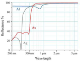
도 3은 본 발명의 일 실시예에 따른 발광 다이오드의 파장에 따른 반사율을 설명하기 위한 그래프이고,
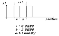
도 4는 본 발명의 일 실시예에 따른 발광 다이오드에서 제2 도전형 반사층을 구성하는 DBR 유닛층의 저 굴절률층과 고 굴절률층에서의 위치에 따른 알루미늄(Al) 함량의 일 예를 나타내는 그래프이고,
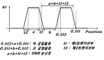
도 5는 본 발명의 일 실시예에 따른 발광 다이오드에서 제2 도전형 반사층을 구성하는 DBR 유닛층의 저 굴절률층과 고 굴절률층에서의 위치에 따른 알루미늄(Al) 함량의 다른 예를 나타내는 그래프이고,
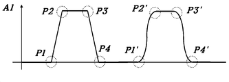
도 6은 도 5의 그래프와 같은 특성을 보이는 알루미늄 함량을 갖는 고 굴절률층과 저 굴절률층에서,제1 트랜지션부와 제2 트랜지션부 각각의 형태를 이차 곡선 형태로 형성한 예를 도5에서와 같은 형태로 형성한 예와 함께 나타낸 그래프이다.이렇게 함으로써 에너지 밴드의 급격한 변화를 줄이고,이에 따라 각 DBR 유닛층에서의 전기적 저항을 낮출 수 있다.
30 : 활성층 40 : 제2 도전형 반도체층
50 : 제2 도전형 반사층
50a, 50b, 50c, ..., 50z : DBR 유닛층
72 : 제2 도전형 중간층 74 : 금속 반사층
80 : 제1 전극
90 : 위상 정합층
Claims (18)
- 전면과 배면을 갖는 제1 도전형 반도체층;
전면과 배면을 갖는 제2 도전형 반도체층;
상기 제1 도전형 반도체층의 배면과 상기 제2 도전형 반도체층의 전면 사이에 형성되는 활성층;
상기 제2 도전형 반도체층의 배면 상에 형성되는 제2 도전형 반사층; 및
상기 제2 도전형 반사층의 배면 상에 형성되어 단파장 대역 및 청색 파장 대역의 광을 반사시키고, 상기 제2 도전형 반도체층과 전기적으로 연결되는 반사부;를 포함하고,
상기 제2 도전형 반사층은 315 nm 내지 420 nm 파장 대역의 광을 반사시키는 DBR(distributed Bragg reflector) 유닛층을 포함하고, 상기 DBR 유닛층은 저 굴절률층과 상기 저 굴절률층에 인접하는 고 굴절률층을 포함하며, 상기 저 굴절률층 및 고 굴절률층 각각은 AlxGa1 -xN(0<x≤1) 및 AlyGa1 -yN(0≤y<1, y<x)을 포함하는 것을 특징으로 하는 발광 다이오드. - 청구항 1에 있어서, 상기 제2 도전형 반도체층과 상기 제2 도전형 DBR 사이에 위상 정합층(phase-matching layer)이 형성되는 것을 특징으로 하는 발광 다이오드.
- 청구항 1에 있어서, 상기 제2 도전형 반사층에서 상기 DBR 유닛층은 세 번 이상 반복되며, 상기 제2 도전형 반도체층의 배면에 가장 가깝게 위치한 최초 세 개의 DBR 유닛층들의 제2 도전형 불순물 도핑 농도인 제1 도핑 농도는 나머지 층의 도핑 농도인 제2 도핑 농도보다 낮은 것을 특징으로 하는 발광 다이오드.
- 청구항 3에 있어서, 상기 제1 도핑 농도는1×1016 cm-3 내지 5×1017 cm- 3 이고, 상기 제2 도핑 농도는 1×1018 cm- 3내지 1×1021cm-3인 것을 특징으로 하는 발광 다이오드.
- 청구항 1에 있어서, 상기 DBR 유닛층이 복수 개인 경우, 상기 반사부에 가장 가깝게 위치한 DBR 유닛층의 제2 도전형 불순물 도핑 농도는 오믹 컨택(Ohmic contact)을 향상시키기 위해 나머지 DBR 유닛층에 비해 더 높은 것을 특징으로 하는 발광 다이오드.
- 청구항 1에 있어서, 상기 반사부는,
오믹 컨택(Ohmic contact)을 향상시키기 위한 제2 도전형 중간층과,
단파장 대역 및 청색 파장 대역의 광을 반사시키기 위한 금속 반사층을 포함하는 것을 특징으로 하는 발광 다이오드. - 청구항 6에 있어서, 상기 금속 반사층은 은(silver)을 포함하는 것을 특징으로 하는 발광 다이오드.
- 청구항 1에 있어서, 상기 제1 도전형 반도체층의 전면에 사파이어 기판이 위치하는 것을 특징으로 하는 발광 다이오드.
- 청구항 1에 있어서, 상기 제1 도전형 반도체층은 n형 반도체층이고, 상기 제2 도전형 반도체층은 p형 반도체층인 것을 특징으로 하는 발광 다이오드.
- 청구항 1에 있어서, 상기 제2 도전형 반도체층은 복수 개의 DBR 유닛층들을 포함하고, 상기 복수 개의 DBR 유닛층들 중 하나의 DBR 유닛층 내에서 저 굴절률층과 고 굴절률층 사이에 Al의 함량이 점진적으로 감소하는 제1 트랜지션부를 포함하고, 상기 하나의 DBR 유닛층의 고 굴절률층과 그 다음의 DBR 유닛층의 저 굴절률층 사이에 Al의 함량이 점진적으로 증가하는 제2 트랜지션부를 포함하는 것을 특징으로 하는 발광 다이오드.
- 청구항 10에 있어서, 상기 제1 트랜지션부 및 상기 제2 트랜지션부 각각은, 시작점과 종료점에 델타 도핑이 적용되는 것을 특징으로 하는 발광 다이오드.
- 청구항 1에 있어서, 상기 제2 도전형 반사층의 두께는 60 nm 내지 1500 nm인 것을 특징으로 하는 발광 다이오드.
- 청구항 1에 있어서, 상기 DBR 유닛층의 두께는 60 nm 내지 100 nm인 것을 특징으로 하는 발광 다이오드.
- 청구항 1에 있어서, 상기 DBR 유닛층에서 상기 저 굴절률층 및 상기 고 굴절률층 각각의 두께는 30 nm 내지 50 nm인 것을 특징으로 하는 발광 다이오드.
- 청구항 6에 있어서, 상기 제2 도전형 중간층의 두께는 10 nm 내지 150 nm인 것을 특징으로 하는 발광 다이오드.
- 청구항 3에 있어서, 상기 위상 정합층은 AlxGa1 -xN(0<x<1)을 포함하는 것을 특징으로 하는 발광 다이오드.
- 청구항 3에 있어서, 상기 위상 정합층의 두께는 5 nm 내지 50 nm인 것을 특징으로 하는 발광 다이오드.
- 청구항 10에 있어서, 상기 제1 트랜지션부 및 상기 제2 트랜지션부 각각의 알루미늄의 함량 프로파일은 선형 또는 이차 곡선인 것을 특징으로 하는 발광 다이오드.
Priority Applications (8)
| Application Number | Priority Date | Filing Date | Title |
|---|---|---|---|
| KR1020160032026A KR20170108321A (ko) | 2016-03-17 | 2016-03-17 | 발광 다이오드 |
| JP2016097186A JP6039848B1 (ja) | 2016-03-17 | 2016-05-13 | 発光ダイオード |
| JP2016216305A JP6320486B2 (ja) | 2016-03-17 | 2016-11-04 | 発光ダイオード |
| US15/356,262 US9853187B2 (en) | 2016-03-17 | 2016-11-18 | Light emitting diode |
| US15/693,159 US9985176B2 (en) | 2016-03-17 | 2017-08-31 | Light emitting diode with reflective part for UVA and blue wavelengths |
| JP2018071697A JP6722221B2 (ja) | 2016-03-17 | 2018-04-03 | 発光ダイオード |
| US15/962,727 US10217899B2 (en) | 2016-03-17 | 2018-04-25 | Light emitting diode with reflective part for UVA and blue wavelengths |
| US16/245,405 US10622512B2 (en) | 2016-03-17 | 2019-01-11 | Light emitting diode with reflective part for UVA and blue wavelengths |
Applications Claiming Priority (1)
| Application Number | Priority Date | Filing Date | Title |
|---|---|---|---|
| KR1020160032026A KR20170108321A (ko) | 2016-03-17 | 2016-03-17 | 발광 다이오드 |
Publications (1)
| Publication Number | Publication Date |
|---|---|
| KR20170108321A true KR20170108321A (ko) | 2017-09-27 |
Family
ID=57483232
Family Applications (1)
| Application Number | Title | Priority Date | Filing Date |
|---|---|---|---|
| KR1020160032026A Ceased KR20170108321A (ko) | 2016-03-17 | 2016-03-17 | 발광 다이오드 |
Country Status (3)
| Country | Link |
|---|---|
| US (4) | US9853187B2 (ko) |
| JP (3) | JP6039848B1 (ko) |
| KR (1) | KR20170108321A (ko) |
Families Citing this family (19)
| Publication number | Priority date | Publication date | Assignee | Title |
|---|---|---|---|---|
| KR20170108321A (ko) * | 2016-03-17 | 2017-09-27 | 주식회사 루멘스 | 발광 다이오드 |
| WO2018151157A1 (ja) * | 2017-02-17 | 2018-08-23 | Dowaエレクトロニクス株式会社 | 深紫外発光素子およびその製造方法 |
| US11282981B2 (en) | 2017-11-27 | 2022-03-22 | Seoul Viosys Co., Ltd. | Passivation covered light emitting unit stack |
| US10892296B2 (en) | 2017-11-27 | 2021-01-12 | Seoul Viosys Co., Ltd. | Light emitting device having commonly connected LED sub-units |
| US11527519B2 (en) | 2017-11-27 | 2022-12-13 | Seoul Viosys Co., Ltd. | LED unit for display and display apparatus having the same |
| US10892297B2 (en) | 2017-11-27 | 2021-01-12 | Seoul Viosys Co., Ltd. | Light emitting diode (LED) stack for a display |
| US12100696B2 (en) | 2017-11-27 | 2024-09-24 | Seoul Viosys Co., Ltd. | Light emitting diode for display and display apparatus having the same |
| US10748881B2 (en) | 2017-12-05 | 2020-08-18 | Seoul Viosys Co., Ltd. | Light emitting device with LED stack for display and display apparatus having the same |
| US10886327B2 (en) | 2017-12-14 | 2021-01-05 | Seoul Viosys Co., Ltd. | Light emitting stacked structure and display device having the same |
| US11552057B2 (en) | 2017-12-20 | 2023-01-10 | Seoul Viosys Co., Ltd. | LED unit for display and display apparatus having the same |
| US11522006B2 (en) | 2017-12-21 | 2022-12-06 | Seoul Viosys Co., Ltd. | Light emitting stacked structure and display device having the same |
| US11552061B2 (en) | 2017-12-22 | 2023-01-10 | Seoul Viosys Co., Ltd. | Light emitting device with LED stack for display and display apparatus having the same |
| JP6727185B2 (ja) * | 2017-12-28 | 2020-07-22 | 日機装株式会社 | 窒化物半導体発光素子 |
| US11114499B2 (en) | 2018-01-02 | 2021-09-07 | Seoul Viosys Co., Ltd. | Display device having light emitting stacked structure |
| US10784240B2 (en) | 2018-01-03 | 2020-09-22 | Seoul Viosys Co., Ltd. | Light emitting device with LED stack for display and display apparatus having the same |
| KR20190104902A (ko) | 2018-03-02 | 2019-09-11 | 마이크로머티어리얼즈 엘엘씨 | 금속 산화물들을 제거하기 위한 방법들 |
| CN110299472B (zh) * | 2019-06-28 | 2022-09-09 | 京东方科技集团股份有限公司 | 一种阵列基板、显示面板及显示装置 |
| TWI893104B (zh) * | 2020-04-21 | 2025-08-11 | 中國大陸商上海顯耀顯示科技有限公司 | 具反射元件之發光二極體晶片結構 |
| CN115843393A (zh) * | 2020-06-03 | 2023-03-24 | 上海显耀显示科技有限公司 | 用于具有水平发光的多色led像素单元的系统和方法 |
Family Cites Families (28)
| Publication number | Priority date | Publication date | Assignee | Title |
|---|---|---|---|---|
| JP2904227B2 (ja) * | 1991-03-08 | 1999-06-14 | 日本電信電話株式会社 | 面発光レーザ |
| US5838707A (en) * | 1996-12-27 | 1998-11-17 | Motorola, Inc. | Ultraviolet/visible light emitting vertical cavity surface emitting laser and method of fabrication |
| JP2001060717A (ja) * | 1999-08-23 | 2001-03-06 | Nippon Sheet Glass Co Ltd | 発光サイリスタおよび自己走査型発光装置 |
| JP2002026385A (ja) * | 2000-07-06 | 2002-01-25 | Hitachi Cable Ltd | 発光ダイオード |
| JP3763737B2 (ja) * | 2000-11-28 | 2006-04-05 | 株式会社東芝 | 半導体発光素子 |
| US20070285000A1 (en) * | 2004-09-10 | 2007-12-13 | Luminus Devices, Inc. | Polarization recycling illumination assembly and methods |
| JP2006100420A (ja) * | 2004-09-28 | 2006-04-13 | Toyoda Gosei Co Ltd | Iii族窒化物系化合物半導体発光素子 |
| TWI267212B (en) * | 2004-12-30 | 2006-11-21 | Ind Tech Res Inst | Quantum dots/quantum well light emitting diode |
| US7498182B1 (en) * | 2005-03-18 | 2009-03-03 | The United States Of America As Represented By The Secretary Of The Army | Method of manufacturing an ultraviolet light emitting AlGaN composition and ultraviolet light emitting device containing same |
| US7928471B2 (en) * | 2006-12-04 | 2011-04-19 | The United States Of America As Represented By The Secretary Of The Navy | Group III-nitride growth on silicon or silicon germanium substrates and method and devices therefor |
| US20090001389A1 (en) * | 2007-06-28 | 2009-01-01 | Motorola, Inc. | Hybrid vertical cavity of multiple wavelength leds |
| JP5237274B2 (ja) * | 2007-06-28 | 2013-07-17 | 京セラ株式会社 | 発光素子及び照明装置 |
| KR101449005B1 (ko) | 2007-11-26 | 2014-10-08 | 엘지이노텍 주식회사 | 반도체 발광소자 및 그 제조방법 |
| JP5378131B2 (ja) * | 2009-09-25 | 2013-12-25 | シャープ株式会社 | 窒化物半導体発光ダイオード素子 |
| US8772805B2 (en) * | 2010-03-31 | 2014-07-08 | Seoul Viosys Co., Ltd. | High efficiency light emitting diode and method for fabricating the same |
| US8927959B2 (en) * | 2010-06-18 | 2015-01-06 | Sensor Electronic Technology, Inc. | Deep ultraviolet light emitting diode |
| US8907322B2 (en) * | 2010-06-18 | 2014-12-09 | Sensor Electronic Technology, Inc. | Deep ultraviolet light emitting diode |
| US10134948B2 (en) * | 2011-02-25 | 2018-11-20 | Sensor Electronic Technology, Inc. | Light emitting diode with polarization control |
| KR101981119B1 (ko) * | 2011-11-25 | 2019-05-22 | 엘지이노텍 주식회사 | 자외선 반도체 발광 소자 |
| EP2791983A4 (en) * | 2011-12-12 | 2015-08-12 | Sensor Electronic Tech Inc | UV REFLECTION CONTACT |
| US8907319B2 (en) * | 2011-12-12 | 2014-12-09 | Lg Innotek Co., Ltd. | Light emitting device package |
| US9312432B2 (en) * | 2012-03-13 | 2016-04-12 | Tsmc Solid State Lighting Ltd. | Growing an improved P-GaN layer of an LED through pressure ramping |
| TW201340405A (zh) * | 2012-03-30 | 2013-10-01 | Lextar Electronics Corp | 發光二極體 |
| KR101370575B1 (ko) | 2012-07-30 | 2014-03-07 | 주식회사 세미콘라이트 | 반도체 발광소자 |
| JP2014103240A (ja) * | 2012-11-20 | 2014-06-05 | Stanley Electric Co Ltd | 半導体発光素子 |
| KR20150136264A (ko) | 2014-05-27 | 2015-12-07 | 서울바이오시스 주식회사 | 발광 소자 |
| TWI689109B (zh) * | 2014-09-04 | 2020-03-21 | 南韓商首爾偉傲世有限公司 | 垂直式紫外線發光裝置及其製造方法 |
| KR20170108321A (ko) * | 2016-03-17 | 2017-09-27 | 주식회사 루멘스 | 발광 다이오드 |
-
2016
- 2016-03-17 KR KR1020160032026A patent/KR20170108321A/ko not_active Ceased
- 2016-05-13 JP JP2016097186A patent/JP6039848B1/ja active Active
- 2016-11-04 JP JP2016216305A patent/JP6320486B2/ja not_active Expired - Fee Related
- 2016-11-18 US US15/356,262 patent/US9853187B2/en not_active Expired - Fee Related
-
2017
- 2017-08-31 US US15/693,159 patent/US9985176B2/en active Active
-
2018
- 2018-04-03 JP JP2018071697A patent/JP6722221B2/ja not_active Expired - Fee Related
- 2018-04-25 US US15/962,727 patent/US10217899B2/en active Active
-
2019
- 2019-01-11 US US16/245,405 patent/US10622512B2/en active Active
Also Published As
| Publication number | Publication date |
|---|---|
| JP6320486B2 (ja) | 2018-05-09 |
| US10622512B2 (en) | 2020-04-14 |
| US10217899B2 (en) | 2019-02-26 |
| US20180069152A1 (en) | 2018-03-08 |
| JP2018113477A (ja) | 2018-07-19 |
| US9985176B2 (en) | 2018-05-29 |
| US20170271555A1 (en) | 2017-09-21 |
| JP6039848B1 (ja) | 2016-12-07 |
| JP2017168811A (ja) | 2017-09-21 |
| US20180240938A1 (en) | 2018-08-23 |
| JP6722221B2 (ja) | 2020-07-15 |
| US9853187B2 (en) | 2017-12-26 |
| US20190148585A1 (en) | 2019-05-16 |
| JP2017168797A (ja) | 2017-09-21 |
Similar Documents
| Publication | Publication Date | Title |
|---|---|---|
| JP6039848B1 (ja) | 発光ダイオード | |
| US8058666B2 (en) | Semiconductor light emitting device and light emitting apparatus having the same | |
| KR101667815B1 (ko) | 발광 소자, 발광 소자 제조방법 및 발광 소자 패키지 | |
| KR100914110B1 (ko) | 반도체 발광 소자 | |
| JP6347600B2 (ja) | 高効率発光ダイオード | |
| US20190393379A1 (en) | Led utilizing internal color conversion with light extraction enhancements | |
| US8440995B2 (en) | Light emitting device, method of manufacturing the same, light emitting device package and lighting system | |
| KR101138976B1 (ko) | 발광다이오드 | |
| US20250022983A1 (en) | Current injection structures for light-emitting diode chips | |
| KR101669640B1 (ko) | 고효율 발광 다이오드 및 그 제조 방법 | |
| KR101754906B1 (ko) | 발광 소자 | |
| JP2012089801A (ja) | 半導体発光素子およびその製造方法、および実装基板 | |
| KR101791159B1 (ko) | 고효율 발광 다이오드 및 그 제조 방법 | |
| KR20160035250A (ko) | 발광 소자 | |
| US10074787B2 (en) | Light emitting diode | |
| KR20170108327A (ko) | 발광 다이오드 | |
| KR101654341B1 (ko) | 발광 소자 및 그 제조방법 | |
| KR101643688B1 (ko) | 반도체 발광소자 | |
| KR101138948B1 (ko) | 고효율 발광 다이오드 | |
| KR101744933B1 (ko) | 고효율 발광 다이오드 | |
| KR20260062268A (ko) | 질화물계 반도체 발광소자 | |
| KR101115537B1 (ko) | 고효율 반도체 발광소자 | |
| KR20190116829A (ko) | 반도체 소자 패키지 | |
| KR20160054332A (ko) | 발광 소자 | |
| KR20160056039A (ko) | 발광소자 및 조명시스템 |
Legal Events
| Date | Code | Title | Description |
|---|---|---|---|
| PA0109 | Patent application |
Patent event code: PA01091R01D Comment text: Patent Application Patent event date: 20160317 |
|
| PG1501 | Laying open of application | ||
| PA0201 | Request for examination |
Patent event code: PA02012R01D Patent event date: 20210216 Comment text: Request for Examination of Application Patent event code: PA02011R01I Patent event date: 20160317 Comment text: Patent Application |
|
| E902 | Notification of reason for refusal | ||
| PE0902 | Notice of grounds for rejection |
Comment text: Notification of reason for refusal Patent event date: 20221014 Patent event code: PE09021S01D |
|
| E601 | Decision to refuse application | ||
| PE0601 | Decision on rejection of patent |
Patent event date: 20230127 Comment text: Decision to Refuse Application Patent event code: PE06012S01D Patent event date: 20221014 Comment text: Notification of reason for refusal Patent event code: PE06011S01I |