WO2019093348A1 - 配線構造及びターゲット材 - Google Patents
配線構造及びターゲット材 Download PDFInfo
- Publication number
- WO2019093348A1 WO2019093348A1 PCT/JP2018/041263 JP2018041263W WO2019093348A1 WO 2019093348 A1 WO2019093348 A1 WO 2019093348A1 JP 2018041263 W JP2018041263 W JP 2018041263W WO 2019093348 A1 WO2019093348 A1 WO 2019093348A1
- Authority
- WO
- WIPO (PCT)
- Prior art keywords
- copper
- zirconium
- layer
- wiring
- intermediate layer
- Prior art date
- Legal status (The legal status is an assumption and is not a legal conclusion. Google has not performed a legal analysis and makes no representation as to the accuracy of the status listed.)
- Ceased
Links
Images

Classifications
-
- C—CHEMISTRY; METALLURGY
- C23—COATING METALLIC MATERIAL; COATING MATERIAL WITH METALLIC MATERIAL; CHEMICAL SURFACE TREATMENT; DIFFUSION TREATMENT OF METALLIC MATERIAL; COATING BY VACUUM EVAPORATION, BY SPUTTERING, BY ION IMPLANTATION OR BY CHEMICAL VAPOUR DEPOSITION, IN GENERAL; INHIBITING CORROSION OF METALLIC MATERIAL OR INCRUSTATION IN GENERAL
- C23C—COATING METALLIC MATERIAL; COATING MATERIAL WITH METALLIC MATERIAL; SURFACE TREATMENT OF METALLIC MATERIAL BY DIFFUSION INTO THE SURFACE, BY CHEMICAL CONVERSION OR SUBSTITUTION; COATING BY VACUUM EVAPORATION, BY SPUTTERING, BY ION IMPLANTATION OR BY CHEMICAL VAPOUR DEPOSITION, IN GENERAL
- C23C14/00—Coating by vacuum evaporation, by sputtering or by ion implantation of the coating forming material
- C23C14/06—Coating by vacuum evaporation, by sputtering or by ion implantation of the coating forming material characterised by the coating material
- C23C14/14—Metallic material, boron or silicon
-
- C—CHEMISTRY; METALLURGY
- C23—COATING METALLIC MATERIAL; COATING MATERIAL WITH METALLIC MATERIAL; CHEMICAL SURFACE TREATMENT; DIFFUSION TREATMENT OF METALLIC MATERIAL; COATING BY VACUUM EVAPORATION, BY SPUTTERING, BY ION IMPLANTATION OR BY CHEMICAL VAPOUR DEPOSITION, IN GENERAL; INHIBITING CORROSION OF METALLIC MATERIAL OR INCRUSTATION IN GENERAL
- C23C—COATING METALLIC MATERIAL; COATING MATERIAL WITH METALLIC MATERIAL; SURFACE TREATMENT OF METALLIC MATERIAL BY DIFFUSION INTO THE SURFACE, BY CHEMICAL CONVERSION OR SUBSTITUTION; COATING BY VACUUM EVAPORATION, BY SPUTTERING, BY ION IMPLANTATION OR BY CHEMICAL VAPOUR DEPOSITION, IN GENERAL
- C23C14/00—Coating by vacuum evaporation, by sputtering or by ion implantation of the coating forming material
- C23C14/22—Coating by vacuum evaporation, by sputtering or by ion implantation of the coating forming material characterised by the process of coating
- C23C14/34—Sputtering
-
- C—CHEMISTRY; METALLURGY
- C23—COATING METALLIC MATERIAL; COATING MATERIAL WITH METALLIC MATERIAL; CHEMICAL SURFACE TREATMENT; DIFFUSION TREATMENT OF METALLIC MATERIAL; COATING BY VACUUM EVAPORATION, BY SPUTTERING, BY ION IMPLANTATION OR BY CHEMICAL VAPOUR DEPOSITION, IN GENERAL; INHIBITING CORROSION OF METALLIC MATERIAL OR INCRUSTATION IN GENERAL
- C23C—COATING METALLIC MATERIAL; COATING MATERIAL WITH METALLIC MATERIAL; SURFACE TREATMENT OF METALLIC MATERIAL BY DIFFUSION INTO THE SURFACE, BY CHEMICAL CONVERSION OR SUBSTITUTION; COATING BY VACUUM EVAPORATION, BY SPUTTERING, BY ION IMPLANTATION OR BY CHEMICAL VAPOUR DEPOSITION, IN GENERAL
- C23C14/00—Coating by vacuum evaporation, by sputtering or by ion implantation of the coating forming material
- C23C14/22—Coating by vacuum evaporation, by sputtering or by ion implantation of the coating forming material characterised by the process of coating
- C23C14/34—Sputtering
- C23C14/3407—Cathode assembly for sputtering apparatus, e.g. Target
-
- H—ELECTRICITY
- H10—SEMICONDUCTOR DEVICES; ELECTRIC SOLID-STATE DEVICES NOT OTHERWISE PROVIDED FOR
- H10D—INORGANIC ELECTRIC SEMICONDUCTOR DEVICES
- H10D64/00—Electrodes of devices having potential barriers
- H10D64/01—Manufacture or treatment
- H10D64/011—Manufacture or treatment of electrodes ohmically coupled to a semiconductor
-
- H—ELECTRICITY
- H10—SEMICONDUCTOR DEVICES; ELECTRIC SOLID-STATE DEVICES NOT OTHERWISE PROVIDED FOR
- H10P—GENERIC PROCESSES OR APPARATUS FOR THE MANUFACTURE OR TREATMENT OF DEVICES COVERED BY CLASS H10
- H10P14/00—Formation of materials, e.g. in the shape of layers or pillars
- H10P14/40—Formation of materials, e.g. in the shape of layers or pillars of conductive or resistive materials
-
- H—ELECTRICITY
- H10—SEMICONDUCTOR DEVICES; ELECTRIC SOLID-STATE DEVICES NOT OTHERWISE PROVIDED FOR
- H10P—GENERIC PROCESSES OR APPARATUS FOR THE MANUFACTURE OR TREATMENT OF DEVICES COVERED BY CLASS H10
- H10P14/00—Formation of materials, e.g. in the shape of layers or pillars
- H10P14/40—Formation of materials, e.g. in the shape of layers or pillars of conductive or resistive materials
- H10P14/412—Deposition of metallic or metal-silicide materials
-
- H—ELECTRICITY
- H10—SEMICONDUCTOR DEVICES; ELECTRIC SOLID-STATE DEVICES NOT OTHERWISE PROVIDED FOR
- H10W—GENERIC PACKAGES, INTERCONNECTIONS, CONNECTORS OR OTHER CONSTRUCTIONAL DETAILS OF DEVICES COVERED BY CLASS H10
- H10W20/00—Interconnections in chips, wafers or substrates
- H10W20/01—Manufacture or treatment
-
- H—ELECTRICITY
- H10—SEMICONDUCTOR DEVICES; ELECTRIC SOLID-STATE DEVICES NOT OTHERWISE PROVIDED FOR
- H10W—GENERIC PACKAGES, INTERCONNECTIONS, CONNECTORS OR OTHER CONSTRUCTIONAL DETAILS OF DEVICES COVERED BY CLASS H10
- H10W20/00—Interconnections in chips, wafers or substrates
- H10W20/40—Interconnections external to wafers or substrates, e.g. back-end-of-line [BEOL] metallisations or vias connecting to gate electrodes
- H10W20/41—Interconnections external to wafers or substrates, e.g. back-end-of-line [BEOL] metallisations or vias connecting to gate electrodes characterised by their conductive parts
- H10W20/425—Barrier, adhesion or liner layers
-
- H—ELECTRICITY
- H10—SEMICONDUCTOR DEVICES; ELECTRIC SOLID-STATE DEVICES NOT OTHERWISE PROVIDED FOR
- H10W—GENERIC PACKAGES, INTERCONNECTIONS, CONNECTORS OR OTHER CONSTRUCTIONAL DETAILS OF DEVICES COVERED BY CLASS H10
- H10W20/00—Interconnections in chips, wafers or substrates
- H10W20/40—Interconnections external to wafers or substrates, e.g. back-end-of-line [BEOL] metallisations or vias connecting to gate electrodes
- H10W20/41—Interconnections external to wafers or substrates, e.g. back-end-of-line [BEOL] metallisations or vias connecting to gate electrodes characterised by their conductive parts
- H10W20/44—Conductive materials thereof
- H10W20/4403—Conductive materials thereof based on metals, e.g. alloys, metal silicides
- H10W20/4421—Conductive materials thereof based on metals, e.g. alloys, metal silicides the principal metal being copper
- H10W20/4424—Copper alloys
-
- H—ELECTRICITY
- H10—SEMICONDUCTOR DEVICES; ELECTRIC SOLID-STATE DEVICES NOT OTHERWISE PROVIDED FOR
- H10W—GENERIC PACKAGES, INTERCONNECTIONS, CONNECTORS OR OTHER CONSTRUCTIONAL DETAILS OF DEVICES COVERED BY CLASS H10
- H10W20/00—Interconnections in chips, wafers or substrates
- H10W20/40—Interconnections external to wafers or substrates, e.g. back-end-of-line [BEOL] metallisations or vias connecting to gate electrodes
- H10W20/45—Interconnections external to wafers or substrates, e.g. back-end-of-line [BEOL] metallisations or vias connecting to gate electrodes characterised by their insulating parts
- H10W20/48—Insulating materials thereof
Definitions
- the present invention relates to a wiring structure.
- the present invention also relates to a target material used for manufacturing the wiring structure.
- An aluminum alloy is often used as a wiring film of a circuit board used for a touch panel of a display device such as a liquid crystal display, a plasma display and an organic EL.
- a display device such as a liquid crystal display, a plasma display and an organic EL.
- miniaturization and thinning of the wiring film have been attempted, and a wiring film having an electrical resistivity lower than that of an aluminum alloy is required. Therefore, copper, which has a low resistance and a high melting point, is drawing attention.
- copper does not have good adhesion to glass or silicon, it is necessary to provide an adhesion layer between the copper wiring film and the substrate made of glass or the like to enhance the adhesion between the two.
- Patent Document 1 describes a technique of providing a barrier layer made of titanium between a glass substrate and a copper thin film which is a main conductive film.
- the barrier layer is considered to have the function of enhancing the adhesion between the glass substrate and the copper thin film.
- Patent Document 2 the adhesion between the SiO 2 substrate and the conductive film is improved by providing the conductive film on the SiO 2 substrate using a sputtering target which is mainly composed of copper and to which zirconium is added. Have been described.
- a layer made of titanium is provided separately from the copper thin film which is the main conductive film. Due to the recent trend toward higher performance of thin film transistors, the process temperature tends to be higher, which makes it easier to cause diffusion of elements between copper and titanium. As a result, the conductivity of the copper thin film may be reduced.
- Patent Document 2 relates to providing a conductive film directly on a substrate to enhance the adhesion between the conductive film and the substrate.
- This conductive film contains zirconium in addition to copper which is the main conductive material. Zirconium has a volume resistance value that is an order of magnitude higher than that of copper, so it is difficult to develop sufficient conductivity if this conductive film is used as it is.
- an object of the present invention is to provide a technique for enhancing the adhesion between a wiring layer and a substrate without deteriorating the conductivity of the wiring layer in a wiring structure provided with a wiring layer containing copper.
- the inventors of the present invention have found that the above problem can be solved by forming an intermediate layer made of a specific alloy between a substrate and a wiring layer containing copper.
- the present invention has been made based on the above findings, and has a wiring structure comprising a glass substrate, an intermediate layer provided on the glass substrate, and a wiring layer provided on the intermediate layer,
- the wiring layer contains copper
- the intermediate layer contains zirconium and the balance is copper and unavoidable impurities.
- the problem is solved by providing a wiring structure in which the ratio of the number of moles of zirconium to the total number of moles of copper and zirconium contained in the intermediate layer is 5% by mole or more and 33% by mole or less.
- the present invention is also a target material used for manufacturing the above wiring structure, It is intended to provide a target material containing zirconium and the balance being copper and unavoidable impurities, or containing zirconium and silicon and the balance being copper and unavoidable impurities.
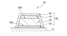
- FIG. 1 is a schematic view of a cross section along the thickness direction showing one embodiment of the wiring structure of the present invention.
- FIG. 2 is a schematic view of a cross section along the thickness direction showing another embodiment of the wiring structure of the present invention.
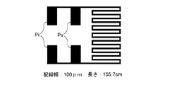
- FIG. 3 is a schematic view of an upper surface of a TEG forming pattern for measuring wiring resistance.
- FIG. 1 shows an embodiment of the wiring structure of the present invention.
- the wiring structure 10 shown in the figure is used as various semiconductor devices such as thin film transistors.
- the wiring structure 10 includes a glass substrate 11.
- the wiring layer containing copper is a wiring of an electrical circuit made of pure copper or a copper alloy, and is generally composed of a thin film layer formed on the glass substrate 11 by various thin film forming methods.
- the thickness of the wiring layer 13 can be arbitrarily set according to the specific application of the wiring structure 10, and can be set to, for example, 100 nm or more and 2000 nm or less.
- the wiring layer 13 is made of a copper alloy
- a copper base alloy containing one or more elements selected from manganese, magnesium, bismuth, indium and the like as alloy components is cited as the copper alloy.
- alloy components can be contained in the copper alloy at a ratio of 0.01 mol% or more and 25 mol% or less.
- the copper alloy is different from or the same as the alloy forming the metal layer 14 described later.
- the wiring layer 13 is made of copper, as long as the wiring layer 13 has the inherent conductivity of copper, it is acceptable that the wiring layer 13 contains a trace amount of other elements other than copper. From the viewpoint of securing conductivity and facilitating etching together with the intermediate layer 12 described later, it is preferably an alloy composed of copper and unavoidable impurities, and has a purity of 3N or more in terms of purity excluding gas components such as oxygen Is more preferred.
- the thickness of the wiring layer 13 is preferably 100 nm or more and 2000 nm or less. By setting the thickness of the wiring layer 13 to 100 nm or more, the conductivity necessary for the wiring structure is secured. Further, by setting the thickness of the wiring layer 13 to 2000 nm or less, it does not become an obstacle when it is used for a multilayer laminated substrate, and it can cope with high definition because it does not become excessively thick in the width direction. Furthermore, mass productivity at the time of circuit board manufacture is unlikely to be impaired. From such a viewpoint, the thickness of the wiring layer 13 is more preferably 150 nm or more and 1200 nm or less, and still more preferably 200 nm or more and 800 nm or less.
- an intermediate layer 12 for improving the adhesion between the two is formed.
- the intermediate layer 12 is in direct contact with the glass substrate 11 and also in direct contact with the wiring layer 13. That is, at the beginning of the film forming process, no layer is interposed between the intermediate layer 12 and the glass substrate 11. Similarly, between the intermediate layer 12 and the wiring layer 13, no layer is initially interposed in the film forming process.
- the intermediate layer 12 is made of a material containing zirconium and the balance being copper and unavoidable impurities. That is, the intermediate layer 12 is made of a copper-zirconium (Cu-Zr) alloy (hereinafter, "the alloy containing zirconium and the balance being copper and unavoidable impurities" is also referred to as “copper-zirconium alloy”).
- Cu-Zr copper-zirconium
- zirconium is an element having low diffusivity with copper, there is an advantage that the conductivity of the wiring layer 13 is unlikely to be reduced even when the wiring structure 10 is used in a high temperature environment.
- the adhesion between the wiring layer 13 and the glass substrate 11 can be enhanced without impairing the conductivity of the wiring layer 13.
- the copper-zirconium alloy can be easily etched by a known etchant such as copper chloride or sulfuric acid / hydrogen peroxide. Therefore, the use of the intermediate layer 12 made of a copper-zirconium alloy has an advantage that a short circuit failure due to a wiring circuit remaining without being dissolved at the time of etching is unlikely to occur. This advantage is also applicable to the case where the copper-zirconium-silicon alloy described later is used as the intermediate layer 12.
- the glass substrate 11 is preferably a glass substrate containing SiO 2 , for example, alkali-free glass, soda lime glass, A borosilicate glass, an aluminosilicate glass, etc. are mentioned, It is especially preferable to use the non-alkali glass substrate for liquid crystal displays.
- the copper-zirconium alloy constituting the intermediate layer 12 has a mole of zirconium to the total number of moles of copper and zirconium.
- the number ratio is preferably 5 to 33 mol%, more preferably 10 to 25 mol%, and still more preferably 12 to 20 mol%.
- the intermediate layer 12 further contains silicon. It is preferable to do. That is, the intermediate layer 12 is a material containing zirconium and silicon and the balance being copper and unavoidable impurities, in other words, a copper-zirconium-silicon (Cu-Zr-Si) alloy (hereinafter referred to as "containing zirconium and silicon, and It is preferable that the alloy is composed of an alloy in which the balance is copper and unavoidable impurities, also referred to as “copper-zirconium-silicon alloy”.
- Cu-Zr-Si copper-zirconium-silicon alloy
- the ratio of the number of moles of zirconium to the total number of moles of copper, zirconium and silicon is 5 mol% or more to 33 moles. It is preferable that it is% or less. From the viewpoint of further improving the adhesion between the wiring layer 13 and the glass substrate 11, the content is preferably 5 mol% or more. Further, it is preferably 33 mol% or less from the viewpoint of improving the etching property in the step of forming the wiring structure and ensuring the ease of film formation in the manufacturing process at the time of forming the intermediate layer.
- the ratio of the number of moles of zirconium to the total number of moles of copper, zirconium and silicon is more preferably 6 mole% or more and 25 mole% or less, and further preferably 7 mole% or more and 20 mole% or less preferable.
- the copper-zirconium-silicon alloy preferably has a ratio of the number of moles of silicon to the total number of moles of copper, zirconium and silicon of 5 to 33 mol%, More preferably, the molar ratio is 25 mol% or less, and more preferably 7 mol% to 20 mol%.
- the ratio of the total number of moles of zirconium and silicon to the total number of moles of copper, zirconium and silicon is 10 mol% or more It is preferable that it is 40 mol% or less. From the viewpoint of further improving the adhesion, 10 mol% or more is preferable. Further, from the viewpoint of keeping the zirconium concentration low to secure the easiness of etching in the step of forming the wiring structure, the content is preferably 40 mol% or less. From such a viewpoint, the ratio of the total number of moles of zirconium and silicon to the total number of moles of copper, zirconium and silicon is preferably 11% to 33% by mole, and 12% to 25% by mole It is further preferred that
- the intermediate layer 12 is made of a copper-zirconium alloy
- the copper-zirconium alloy is an alloy containing zirconium and the balance being copper and an unavoidable impurity, as described above.
- the intermediate layer 12 is composed of a copper-zirconium-silicon alloy
- the copper-zirconium-silicon alloy is an alloy containing zirconium and silicon and the balance being copper and an unavoidable impurity as described above. Is preferred. Even when the intermediate layer is made of any of these alloys, it is acceptable that these alloys contain copper, zirconium and other elements other than silicon to a small extent to the extent that the effects of the present invention are exhibited.
- the ratio of unavoidable impurities is the sum of the number of moles of copper and zirconium or the sum of the number of moles of copper, zirconium and silicon Is preferably 2 mol% or less, and more preferably 1 mol% or less. The smaller the proportion of unavoidable impurities, the better.
- the intermediate layer 12 can be formed, for example, by various thin film formation methods.
- a thin film formation method conventionally known methods such as sputtering and vacuum evaporation can be adopted.
- a target material containing zirconium as the copper-zirconium alloy source or copper-zirconium-silicon alloy source and the balance containing copper and unavoidable impurities or the balance with zirconium and silicon It is preferable to use a target material consisting of copper and unavoidable impurities.
- the alloy composition in this target material is the same as the composition of the alloy constituting the intermediate layer 12, and may have the same composition.
- the target material is made of a copper-zirconium alloy or a copper-zirconium-silicon alloy, and in the wiring structure 10, the intermediate layer 12 for improving the adhesion between the glass substrate 11 and the wiring layer 13. It is used for formation.
- this target material contains a trace amount of other elements than copper, zirconium and silicon, for example, oxygen, for the same reason as the intermediate layer 12, the content of the element is as small as possible. Is preferred.
- the target material is a sputtering target made of a copper-zirconium-silicon alloy
- the proportion of the copper-zirconium-silicon alloy in the target makes the improvement in the adhesion between the intermediate layer 12 and the glass substrate 11 more remarkable.
- it is preferably 6% or more and 40% or less, more preferably 9% or more and 40% or less, and most preferably 15% or more and 35% or less.
- the above ratio is calculated by the method described in [Proportion of copper-zirconium-silicon alloy in sputtering target] in the examples described later.
- the target material described above is suitably used not only for sputtering but also as a target material for various physical vapor deposition (PVD) methods such as vacuum deposition such as arc ion plating.
- PVD physical vapor deposition
- the above target material can be manufactured by various methods known in the art. For example, copper and zirconium melted in vacuum and optionally silicon are used as raw materials, cast and alloyed. Next, a target material is manufactured using the obtained ingot.
- a target material is manufactured using the obtained ingot.
- it may be hot forging, may be cold forging, or may be hot rolling. Moreover, it cuts out with a wire saw, and you may form in a board
- the obtained plate material may be attached to a backing plate which is a jig for sputtering using a bonding material such as indium.
- the target material also includes the state before the target material finishing process such as surface grinding and bonding.
- the shape of the target material is not limited to a flat plate, and includes a cylindrical shape.
- the sputtering target refers to one which is subjected to sputtering by bonding one or more target materials to a backing plate or the like.
- the thickness of the intermediate layer 12 formed by the above-mentioned method is preferably 10 nm or more and 100 nm or less.
- the intermediate layer 12 can be formed all over the glass substrate 11, and the adhesion between the glass substrate 11 and the wiring layer 13 can be surely improved.
- productivity in manufacturing can be prevented from being impaired without unnecessarily increasing the volume resistivity of the wiring structure.
- the thickness of the intermediate layer 12 can be arbitrarily set within the above range as long as the adhesion between the glass substrate 11 and the wiring layer 13 is improved, more preferably 15 nm or more and 80 nm or less, still more preferably 20 nm or more and 50 nm or less It can be set to
- the wiring layer 13 has a first surface 13 a which is a surface facing the glass substrate 11. Further, the wiring layer 13 has a second surface 13 b which is a surface opposite to the first surface 13 a. The first surface 13 a is in contact with the intermediate layer 12 described above.
- the metal layer 14 is provided on the second surface 13 b. The wiring layer 13 and the metal layer 14 are in direct contact with each other, and no other layer is interposed between the two layers 13 and 14. The metal layer 14 is formed to cover the entire area of the second surface 13 b of the wiring layer 13. Therefore, the region exposed to the second surface 13b of the wiring layer 13 does not exist.
- the adhesion between the substrate 11 and the intermediate layer 12 and the adhesion between the intermediate layer 12 and the wiring layer 13 via the first surface 13 a are important.
- the temperature of this annealing treatment is generally 100 ° C. or higher, more preferably 300 ° C. or higher, and still more preferably 500 ° C. or higher.
- the annealing time is generally 15 minutes or more and 120 minutes or less.
- the annealing may be performed after the film formation of the wiring layer 13, after the film formation of the metal layer 14 or the insulating layer 15 described later, or after the patterning of the resist.
- the film forming process may be performed simultaneously with the above-described annealing conditions.
- the insulating layer 15 is provided on the wiring layer 13.
- the insulating layer 15 is additionally provided for the purpose of preventing the oxidation of the wiring layer 13 and preventing a short circuit due to a foreign matter or the like.
- the insulating layer 15 is made of a highly oxidation resistant material.
- the material having high oxidation resistance include nitrides, carbides, and oxides.
- non-oxides include nitrides and carbides.
- the use of nitrides is preferable from the viewpoint of maximizing the oxidation resistance.
- nitride for example, a metal or metalloid nitride is suitably used, and examples thereof include silicon nitride which is a material capable of forming a film in a reducing atmosphere and suppressing the progress of oxidation of the wiring layer 13 .
- silicon nitride which is a material capable of forming a film in a reducing atmosphere and suppressing the progress of oxidation of the wiring layer 13 .
- oxide an oxide containing silicon such as SiO 2 and an oxide containing a rare earth such as Y 2 O 3 are preferable from the viewpoint of the stability of the thin film transistor.
- the insulating layer 15 is provided so as to cover the entire surface including the side surfaces of the wiring layer 13 and the intermediate layer 12 from the viewpoint of maximizing the oxidation resistance. Instead of this, the insulating layer may be provided only in the entire region on the second surface 13 b side of the wiring layer 13.
- the wiring structure 10 of the present embodiment includes an insulating layer 15 on the wiring layer 13.
- a metal layer 14 is disposed between the wiring layer 13 and the insulating layer 15. The metal layer 14 is in direct contact with the wiring layer 13 and also in direct contact with the insulating layer 15 at the beginning of the film forming process.
- the metal layer 14 is a layer additionally used. By providing the metal layer 14 on the wiring layer 13 and below the insulating layer 15 as shown in FIG. 2, the oxidation of the wiring layer 13 is more effectively prevented.
- the metal layer 14 and the insulating layer 15 can be alternatively used to prevent the oxidation of the wiring layer 13. That is, only the metal layer 14 may be provided on the wiring layer 13, or only the insulating layer 15 may be provided on the wiring layer 13. Also, as in the present embodiment, the metal layer 14 and the insulating layer 15 may be provided in this order on the wiring layer 13.
- the film formation of the insulating layer 15 is generally performed in a state where the substrate temperature is raised.
- the thickness of the insulating layer 15 may be set to such an extent that oxidation of the wiring layer 13 can be prevented, preferably 50 nm to 500 nm, and more preferably 80 nm to 300 nm. It can be set.
- an alloy containing zirconium and the balance of copper and unavoidable impurities ie, a copper-zirconium alloy is used.
- an alloy containing zirconium and silicon and the balance being copper and unavoidable impurities, ie, a copper-zirconium-silicon alloy is used.
- the wiring structure 10 is not easily affected by the oxidation caused by the annealing even after the annealing in the oxidizing atmosphere.
- the copper-zirconium alloy constituting the metal layer 14 has a ratio of the number of moles of zirconium to the total number of moles of copper and zirconium of 5 to 33 mol%. % Or less is preferable, 5 to 25 mol% is more preferable, and 10 to 20 mol% is more preferable.
- the copper-zirconium-silicon alloy has a ratio of the number of moles of zirconium to the total number of moles of copper, zirconium and silicon from the viewpoint of imparting heat resistance. 1 mol% or more is preferable.
- the content is preferably 33 mol% or less, and more preferably 1 mol% to 25 mol%. It is more preferably 2 mol% or more and 20 mol% or less, and still more preferably 4 mol% or more and 10 mol% or less.
- the ratio of the number of moles of silicon to the total number of moles of copper, zirconium and silicon is 1% to 33% by mole. Is more preferably 1 to 25 mol%, still more preferably 2 to 20 mol%, and still more preferably 4 to 10 mol%.
- the copper-zirconium-silicon alloy is composed of copper, zirconium and silicon
- the ratio of the total number of moles of zirconium and silicon to the total number is preferably 2 mol% or more and 40 mol% or less, more preferably 2 mol% or more and 25 mol% or less, and more preferably 4 mol% or more It is more preferable that it is mol% or less, and it is still more preferable that it is 8 mol% or more and 16 mol% or less.
- the copper-zirconium alloy or the copper-zirconium-silicon alloy constituting the metal layer 14 is, as described above, an alloy containing zirconium and the balance being copper and an unavoidable impurity, or containing zirconium and silicon, and the balance Is preferably an alloy of copper and unavoidable impurities.
- the alloy contains copper, zirconium and other elements other than silicon to such an extent that the effects of the present invention can be achieved.
- the ratio of unavoidable impurities is the sum of the number of moles of copper and zirconium or the sum of the number of moles of copper, zirconium and silicon Is preferably 2 mol% or less, and more preferably 1 mol% or less. The smaller the proportion of unavoidable impurities, the better.
- the metal layer 14 can be formed, for example, by various thin film formation methods. As a thin film formation method, conventionally known methods such as sputtering and vacuum evaporation can be adopted.
- the thickness of the metal layer 14 can be arbitrarily set according to the specific use of the wiring structure 10, and can be set to, for example, 10 nm or more and 100 nm or less. By setting the thickness of the metal layer 14 to 10 nm or more, the oxidation of copper contained in the wiring layer 13 to be protected can be effectively prevented. Further, by setting the thickness of the metal layer 14 to 100 nm or less, the productivity of the metal layer 14 can be prevented from being impaired.
- the metal layer 14 may cover a portion necessary to achieve the purpose of preventing the oxidation of the wiring layer 13.
- the wiring layer 13 is provided only on the entire area on the second surface 13 b side, but may be provided so as to cover the whole including the side surfaces of the wiring layer 13 and the intermediate layer 12 as necessary.
- Wiring structure 10 includes a step of providing intermediate layer 12 on glass substrate 11, a step of providing wiring layer 13 containing copper on intermediate layer 12, a step of providing metal layer 14 on wiring layer 13, and these layers. Heat treating the laminated structure having 12, 13, and 14 preferably. Then, according to this manufacturing method, in the process of manufacturing the wiring structure 10, the oxidation of the wiring layer 13 can be prevented even when the heat treatment is performed in an oxidizing atmosphere such as under the air.
- the adhesion between the glass substrate 11 and the wiring layer 13, (ii) the element which is an advantage of the wiring structure of the embodiment shown in FIG.
- the contradictory characteristics of (iv) suppression of oxidation of the wiring layer 13 can all be satisfied. There is an advantage.
- the wiring structure 10 of each of the above embodiments may be used as it is or may be post-processed and used as various electronic devices.
- various semiconductor devices such as a thin film transistor, are mentioned, for example.
- the present invention has been described above based on its preferred embodiments, the present invention is not limited to the embodiments.
- the insulating layer 15 is provided on the wiring layer 13, but the insulating layer 15 may not be provided.
- the metal layer 14 and the insulating layer 15 are provided on the wiring layer 13, but the insulating layer 15 may not be provided.
- Example 1 Ingots of various starting materials were precisely weighed so as to obtain the compositions shown in Table 1 below, and these ingots were charged into a carbon crucible. These ingots were vacuum heated and melted in a high frequency induction vacuum melting furnace. The molten metal thus obtained was cast with a carbon mold to obtain an ingot. The obtained ingot was cut out using a wire saw and then processed to a thickness of 5 mm by lathe processing. One surface of the target material thus obtained was brazed with indium to a backing plate to prepare a copper-zirconium-silicon alloy sputtering target for an intermediate layer.
- the wiring structure was manufactured using the copper-zirconium-silicon alloy sputtering target for the intermediate layer obtained above and the pure copper sputtering target of 6N purity.
- sputtering was performed under the following conditions to form an intermediate layer with a thickness of 25 nm on a glass substrate.
- sputtering was performed using a pure copper sputtering target under the same conditions to form a 400 nm thick wiring layer on the intermediate layer.
- ⁇ sputtering conditions >> ⁇ Sputtering method: DC magnetron sputtering ⁇ Evacuation device: Rotary pump + cryo pump ⁇ Achieved degree of vacuum: 1 ⁇ 10 -4 Pa or less ⁇ Ar pressure: 0.4 Pa Substrate temperature: 100 ° C. Sputtering power: 1000 W (power density 3.1 W / cm 2 ) -Substrate used: EAGLE XG (Corning / non-alkali glass for liquid crystal display, registered trademark), 50 mm (longitudinal) x 50 mm (horizontally) x 0.7 mm (thickness)
- Examples 2 to 4 The amounts of copper, zirconium and silicon were changed so that the proportions of copper, zirconium and silicon were as shown in Table 1, and a copper-zirconium-silicon alloy sputtering target was produced.
- An intermediate layer was obtained as in Example 1 using the obtained sputtering target.
- a copper-zirconium-silicon alloy sputtering target for a metal layer having the same composition as the intermediate layer is used to carry out sputtering under the same conditions as the intermediate layer to form a 50 nm thick metal layer on the wiring layer. It formed.
- a wiring structure shown in FIG. 2 was obtained in the same manner as in Example 1 except for the above.
- Examples 5 and 6 An intermediate layer was obtained in the same manner as in Example 1 except that a copper-zirconium alloy sputtering target having a composition shown in Table 1 was used instead of the copper-zirconium-silicon alloy sputtering target used in Example 1. Furthermore, an insulating layer was formed on the intermediate layer by the same method as in Example 1 to obtain a wiring structure shown in FIG.
- Example 1 Comparative Example 1 In Example 1, an intermediate layer made of a copper-zirconium-silicon alloy was not formed. A wiring structure was obtained in the same manner as in Example 1 except for the above.
- Comparative Example 4 Instead of using a copper-zirconium-silicon alloy sputtering target for forming the intermediate layer, a copper-zirconium alloy sputtering target having the composition shown in Table 1 was used. A wiring structure was obtained in the same manner as in Example 1 except for these.
- Comparative Example 5 Instead of using a copper-zirconium-silicon alloy sputtering target for forming the intermediate layer, a copper-zirconium alloy sputtering target having the composition shown in Table 1 was used. Moreover, the wiring layer which consists of copper on an intermediate
- Comparative Example 6 Instead of using a copper-zirconium-silicon alloy sputtering target for forming the intermediate layer, a copper-zirconium-silicon alloy sputtering target having the composition shown in Table 1 was used. A wiring structure was obtained in the same manner as in Example 1 except for the above.
- peel test The peel test was performed in accordance with JIS K5600-5-6. Twenty-five grids of 1 mm ⁇ 1 mm were formed on the laminated structure using an NT cutter eL-500. A tape 8705 B made by TQC was attached to the lattice cut portion, and the tape was rubbed with a finger so that the laminated structure could be seen through. The tape was peeled off within 5 minutes after the tape was attached. What peeled in the area
- the volume resistivity of the obtained wiring structure was measured before and after the annealing treatment.
- a four-terminal resistance measuring apparatus (B-1500A: manufactured by Agilent Technologies) was used. The measurement procedure is shown below.
- the wiring resistance of the conductive portion composed of the metal layer and the wiring layer is measured in advance in the state of the laminated structure before the annealing process. Specifically, the current value is swept between the current application pads Pi and Pi shown in FIG. 3, and the voltage value between the voltage measurement pads Pv and Pv is measured to obtain the wiring resistance value.
- the volume resistivity of the conductive portion is calculated from the obtained wiring resistance value, the line width, the length, and the film thickness of the conductive portion. The value is taken as the volume resistivity ( ⁇ ⁇ cm) before annealing.
- the volume resistivity is calculated by the same method as the measurement of the volume resistivity before the annealing process. The value is taken as the volume resistivity ( ⁇ ⁇ cm) after annealing. Then, the rate of change in volume resistivity before and after the annealing process is calculated. The rate of change in volume resistivity (%) is calculated from ⁇ (volume resistivity after annealing ⁇ volume resistivity before annealing) / volume resistivity before annealing ⁇ ⁇ 100.
- the ratio of the copper-zirconium-silicon alloy in the sputtering target is energy dispersive X-ray (EDX) analysis on the surface of the sputtering target material used for manufacturing the wiring structures of Examples 1 to 4 and Comparative Example 6. Calculated by Specifically, elemental analysis was performed using an energy dispersive X-ray analyzer (Dry SD 100 GV, manufactured by Nippon Denshi Co., Ltd.).
- the phase separation was performed using multivariate image analysis software (NSS4 manufactured by Thermo Fisher Scientific Co., Ltd.) to the analysis results, and the ratio (%) of the area of the copper-zirconium-silicon alloy to the area of the entire image was calculated. .
- Example 5 the obtained peak was analyzed using analysis software (Multipack 9.0 manufactured by ULVAC-PHI, Inc.) to determine the binding energy of the Zr3d electron.
- a peak was observed at a location corresponding to the oxide of Zr.
- a peak was observed on the higher energy side than Example 5. From the above results, it can be seen that the adhesion is ensured by the fact that Zr added to Cu bonds with the surface of the glass substrate as an oxide. Further, it can be seen that the adhesion is further enhanced by adding both Zr and Si to Cu.
- Comparative Example 5 when the Zr concentration in Cu is increased to 5%, the volume resistivity is rapidly increased, and the conductivity is inferior only with the Cu—Zr alloy layer having such a composition. Furthermore, it can be seen that in the wiring structures of the first to fourth embodiments, the formation of the wiring pattern by etching can be performed extremely well.
- the adhesion between the wiring layer and the substrate can be enhanced without impairing the conductivity of the wiring layer.
Landscapes
- Chemical & Material Sciences (AREA)
- Chemical Kinetics & Catalysis (AREA)
- Engineering & Computer Science (AREA)
- Materials Engineering (AREA)
- Mechanical Engineering (AREA)
- Metallurgy (AREA)
- Organic Chemistry (AREA)
- Internal Circuitry In Semiconductor Integrated Circuit Devices (AREA)
- Physical Vapour Deposition (AREA)
Abstract
Description
前記配線層は銅を含み、
前記中間層はジルコニウムを含み、且つ残部が銅及び不可避不純物からなり、
前記中間層に含まれる銅及びジルコニウムのモル数の合計に対するジルコニウムのモル数の割合が5モル%以上33モル%以下である配線構造を提供することにより前記課題を解決したものである。
ジルコニウムを含み、且つ残部が銅及び不可避不純物からなるか、又はジルコニウム及びケイ素を含み、且つ残部が銅及び不可避不純物からなるターゲット材を提供するものである。
また、ターゲット材の形状は平板に限定されず、円筒形状のものも含まれる。本発明においてスパッタリングターゲットとは、こうした単数又は複数のターゲット材をバッキングプレート等にボンディングされるなどしてスパッタリングに供されるものをいう。
このアニール処理は配線層13の成膜後であれば、金属層14や、後述する絶縁層15の成膜後やレジストのパターニング後でもよい。また上述のアニール条件を満たす範囲で成膜工程と同時に行っても良い。
以下の表1に示す組成となるように、各種出発原料のインゴットを精秤して、これらインゴットをカーボン製の坩堝に投入した。高周波誘導真空溶解炉中でこれらのインゴットを真空加熱して溶融させた。それによって得た溶湯をカーボン製の鋳型で鋳造し、鋳塊を得た。得られた鋳塊を、ワイヤーソーを用いて切り出した後、旋盤加工によって厚み5mmに加工した。このようにして得られたターゲット材の一面を、バッキングプレートにインジウムでロウ付けし、中間層用の銅-ジルコニウム-ケイ素合金スパッタリングターゲットを作製した。
・スパッタ方式:DCマグネトロンスパッタ
・排気装置 :ロータリーポンプ+クライオポンプ
・到達真空度 :1×10⁻⁴Pa以下
・Ar圧力 :0.4Pa
・基板温度 :100℃・スパッタ電力:1000W(電力密度3.1W/cm2)
・使用基板 :EAGLE XG(コーニング社/液晶ディスプレイ用無アルカリガラス、登録商標)、50mm(縦)×50mm(横)×0.7mm(厚み)
・成膜ガス:SiH4:10cm3/min、H2:90cm3/min、NH3:10cm3/min、N2:210cm3/min
・成膜温度:350℃
・成膜圧力:80Pa・電力:250W
銅、ジルコニウム及びケイ素の割合が表1に示す値となるように仕込み量を変更し、銅-ジルコニウム-ケイ素合金スパッタリングターゲットを作製した。得られたスパッタリングターゲットを用い、実施例1と同様にして中間層を得た。更に、各実施例において中間層と同一組成の金属層用の銅-ジルコニウム-ケイ素合金スパッタリングターゲットを用い、中間層と同条件でスパッタリングを実施して、該配線層上に厚み50nmの金属層を形成した。これ以外は実施例1と同様にして図2に示す配線構造を得た。
実施例1で用いた銅-ジルコニウム-ケイ素合金スパッタリングターゲットに代えて、表1に示す組成の銅-ジルコニウム合金スパッタリングターゲットを用い、これ以外は実施例1と同様にして中間層を得た。更に中間層上に実施例1と同様の方法により絶縁層を形成し、図1に示す配線構造を得た。
実施例1において、銅-ジルコニウム-ケイ素合金からなる中間層を形成しなかった。これ以外は実施例1と同様にして配線構造を得た。
中間層の形成に、銅-ジルコニウム-ケイ素合金スパッタリングターゲットを用いることに代えて、チタンのスパッタリングターゲット(比較例2)及びモリブデンのスパッタリングターゲット(比較例3)を用いた。これ以外は実施例1と同様にして、配線構造を得た。
中間層の形成に、銅-ジルコニウム-ケイ素合金スパッタリングターゲットを用いることに代えて、表1に示す組成を有する銅-ジルコニウム合金スパッタリングターゲットを用いた。これら以外は実施例1と同様にして、配線構造を得た。
中間層の形成に、銅-ジルコニウム-ケイ素合金スパッタリングターゲットを用いることに代えて、表1に示す組成を有する銅-ジルコニウム合金スパッタリングターゲットを用いた。また、中間層上の銅からなる配線層を形成しなかった。これら以外は実施例1と同様にして、配線構造を得た。
中間層の形成に、銅-ジルコニウム-ケイ素合金スパッタリングターゲットを用いることに代えて、表1に示す組成を有する銅-ジルコニウム-ケイ素合金スパッタリングターゲットを用いた。これ以外は実施例1と同様にして、配線構造を得た。
実施例及び比較例で得られた配線構造について、以下の方法でピール試験を行い、また耐酸化性及びエッチング容易性を以下の方法で評価した。更に、実施例及び比較例で用いたスパッタリングターゲット中の銅-ジルコニウム-ケイ素合金の割合を以下の方法で評価した。それらの結果を表1に示す。
JIS K5600-5-6に準拠しピール試験を行った。NTカッターeL-500を用いて積層構造に、1mm×1mmの格子パターンを25マス形成した。TQC社製テープ8705Bを格子カット部分に貼り、積層構造が透けて見えるように指でテープをこすった。テープ付着後5分以内にテープを引きはがした。格子マスのうち5%を超える領域が剥離したものを剥離個数としてカウントした。
得られた配線構造の体積抵抗率をアニール処理前とアニール処理後のそれぞれで測定した。測定には4端子抵抗測定装置(B-1500A:アジレントテクノロジー社製)を用いた。測定手順を以下に示す。
まず、配線構造の製造時において、アニール処理前の積層構造の状態で、予め金属層及び配線層からなる導電部の配線抵抗を測定する。具体的には、図3に示す電流印加パッドPi,Pi間で電流値を掃引させ、電圧測定パッドPv,Pv間の電圧値を測定することで配線抵抗値を得る。得られた配線抵抗値、前記導電部の線幅、長さ、及び膜厚より、導電部の体積抵抗率を算出する。その値をアニール処理前の体積抵抗率(Ω・cm)とする。
次に、アニール処理後の配線構造において、アニール処理前の体積抵抗率の測定と同様の方法で体積抵抗率を算出する。その値をアニール処理後の体積抵抗率(Ω・cm)とする。
そして、アニール処理前とアニール処理後での体積抵抗率の変化率を算出する。体積抵抗率の変化率(%)は、{(アニール処理後の体積抵抗率-アニール処理前の体積抵抗率)/アニール処理前の体積抵抗率}×100から算出する。
実施例及び比較例で得られた配線構造を硫酸過水でエッチングした。エッチング後の配線構造をSEMによって観察し、配線パターンの形成の良否を以下の基準で評価した。
E:配線パターンが極めて明確である。
G:配線パターンが明確である。
P:中間層が基板上に残留している部分が多く観察される。
スパッタリングターゲット中の銅-ジルコニウム-ケイ素合金の割合は、実施例1ないし4、及び比較例6の配線構造の製造に用いたスパッタリングターゲット材の表面を対象として、エネルギー分散型X線(EDX)分析により算出した。詳細には、エネルギー分散型X線分析装置(日本電子社製、ドライSD100GV)を用いて、元素分析を行った。分析結果に対して多変量イメージ解析ソフト(サーモフィッシャーサイエンティフィック社製、NSS4)を用いて相分離を行い、画像全体の面積に対する銅-ジルコニウム-ケイ素合金の面積の割合(%)を算出した。
中間層とガラス基板の密着力の起源を調査するため、実施例2、4及び5の配線構造を硝酸+過酸化水素系のエッチャントを用いてエッチング後、ガラス基板の表面をXPS(アルバック・ファイ社製、Versa ProveIII)により下記条件で測定した。
・出力:50W
・X線径:200μmφ
・Pass Energy:26eV
・エネルギーステップ:0.1eV
・Take of Angle:45°
・帯電中和:低速イオン銃及び電子銃使用
実施例5において、Zrの酸化物に相当する箇所にピークが見られた。実施例2及び4においては、実施例5よりも高エネルギー側にピークが認められた。
以上の結果から、Cuに添加されたZrが酸化物としてガラス基板の表面と結合することで密着性が担保されていることが分かる。また、CuにZrとSiを共に添加することで更に密着力が強くなっていることが分かる。

更に、実施例1ないし4の配線構造は、エッチングによる配線パターンの形成が極めて良好に行えることが判る。
Claims (10)
- ガラス基板と、該ガラス基板上に設けられた中間層と、該中間層上に設けられた配線層とを備えた配線構造であって、
前記配線層は銅を含み、
前記中間層はジルコニウムを含み、且つ残部が銅及び不可避不純物からなり、
前記中間層に含まれる銅及びジルコニウムのモル数の合計に対するジルコニウムのモル数の割合が5モル%以上33モル%以下である配線構造。 - 前記中間層が更にケイ素を含有する請求項1に記載の配線構造。
- 前記中間層に含まれる銅、ジルコニウム及びケイ素のモル数の合計に対するジルコニウムのモル数の割合が5モル%以上33モル%以下であり、ケイ素のモル数の割合が5モル%以上33モル%以下である請求項2に記載の配線構造。
- 前記配線層上に、絶縁層を備えた請求項1ないし3のいずれか一項に記載の配線構造。
- 前記絶縁層が窒化物からなる請求項4に記載の配線構造。
- 前記窒化物が窒化ケイ素からなる請求項5に記載の配線構造。
- 前記配線層上と前記絶縁層の間に金属層を備え、該金属層はジルコニウムを含み、且つ残部が銅及び不可避不純物からなる、請求項4ないし6のいずれか一項に記載の配線構造。
- 前記金属層が更にケイ素を含有する請求項7に記載の配線構造。
- 請求項1に記載の配線構造の製造に用いるターゲット材であって、
ジルコニウムを含み、且つ残部が銅及び不可避不純物からなるターゲット材。 - 請求項3に記載の配線構造の製造に用いるターゲット材であって、
ジルコニウム及びケイ素を含み、且つ残部が銅及び不可避不純物からなるターゲット材。
Priority Applications (3)
| Application Number | Priority Date | Filing Date | Title |
|---|---|---|---|
| JP2019552825A JPWO2019093348A1 (ja) | 2017-11-09 | 2018-11-07 | 配線構造及びターゲット材 |
| KR1020207010987A KR20200078494A (ko) | 2017-11-09 | 2018-11-07 | 배선 구조 및 타깃재 |
| CN201880065146.0A CN111183508A (zh) | 2017-11-09 | 2018-11-07 | 布线结构及靶材 |
Applications Claiming Priority (2)
| Application Number | Priority Date | Filing Date | Title |
|---|---|---|---|
| JP2017-216372 | 2017-11-09 | ||
| JP2017216372 | 2017-11-09 |
Publications (1)
| Publication Number | Publication Date |
|---|---|
| WO2019093348A1 true WO2019093348A1 (ja) | 2019-05-16 |
Family
ID=66437788
Family Applications (1)
| Application Number | Title | Priority Date | Filing Date |
|---|---|---|---|
| PCT/JP2018/041263 Ceased WO2019093348A1 (ja) | 2017-11-09 | 2018-11-07 | 配線構造及びターゲット材 |
Country Status (5)
| Country | Link |
|---|---|
| JP (1) | JPWO2019093348A1 (ja) |
| KR (1) | KR20200078494A (ja) |
| CN (1) | CN111183508A (ja) |
| TW (1) | TW201928074A (ja) |
| WO (1) | WO2019093348A1 (ja) |
Citations (6)
| Publication number | Priority date | Publication date | Assignee | Title |
|---|---|---|---|---|
| JP2008112989A (ja) * | 2006-10-05 | 2008-05-15 | Ulvac Japan Ltd | ターゲット、成膜方法、薄膜トランジスタ、薄膜トランジスタ付パネル、及び薄膜トランジスタの製造方法 |
| JP2009060009A (ja) * | 2007-09-03 | 2009-03-19 | Sharp Corp | 結晶質半導体膜の製造方法およびアクティブマトリクス基板の製造方法 |
| WO2009128372A1 (ja) * | 2008-04-15 | 2009-10-22 | 株式会社アルバック | 薄膜トランジスタ、薄膜トランジスタの製造方法 |
| JP2010185139A (ja) * | 2009-01-16 | 2010-08-26 | Kobe Steel Ltd | Cu合金膜および表示デバイス |
| JP2010248619A (ja) * | 2009-03-26 | 2010-11-04 | Hitachi Metals Ltd | 酸素含有Cu合金膜の製造方法 |
| JP2016178286A (ja) * | 2015-03-20 | 2016-10-06 | 日立金属株式会社 | 電子部品用積層配線膜および被覆層形成用スパッタリングターゲット材 |
Family Cites Families (3)
| Publication number | Priority date | Publication date | Assignee | Title |
|---|---|---|---|---|
| JPH03196619A (ja) | 1989-12-26 | 1991-08-28 | Nippon Mining Co Ltd | 銅配線の形成法とそれに使用するターゲット |
| US8647980B2 (en) | 2010-02-25 | 2014-02-11 | Sharp Kabushiki Kaisha | Method of forming wiring and method of manufacturing semiconductor substrates |
| KR20170118586A (ko) * | 2015-02-19 | 2017-10-25 | 미쓰이금속광업주식회사 | 구리 기반 합금 스퍼터링 타겟 |
-
2018
- 2018-11-07 KR KR1020207010987A patent/KR20200078494A/ko not_active Withdrawn
- 2018-11-07 WO PCT/JP2018/041263 patent/WO2019093348A1/ja not_active Ceased
- 2018-11-07 JP JP2019552825A patent/JPWO2019093348A1/ja active Pending
- 2018-11-07 CN CN201880065146.0A patent/CN111183508A/zh active Pending
- 2018-11-08 TW TW107139633A patent/TW201928074A/zh unknown
Patent Citations (6)
| Publication number | Priority date | Publication date | Assignee | Title |
|---|---|---|---|---|
| JP2008112989A (ja) * | 2006-10-05 | 2008-05-15 | Ulvac Japan Ltd | ターゲット、成膜方法、薄膜トランジスタ、薄膜トランジスタ付パネル、及び薄膜トランジスタの製造方法 |
| JP2009060009A (ja) * | 2007-09-03 | 2009-03-19 | Sharp Corp | 結晶質半導体膜の製造方法およびアクティブマトリクス基板の製造方法 |
| WO2009128372A1 (ja) * | 2008-04-15 | 2009-10-22 | 株式会社アルバック | 薄膜トランジスタ、薄膜トランジスタの製造方法 |
| JP2010185139A (ja) * | 2009-01-16 | 2010-08-26 | Kobe Steel Ltd | Cu合金膜および表示デバイス |
| JP2010248619A (ja) * | 2009-03-26 | 2010-11-04 | Hitachi Metals Ltd | 酸素含有Cu合金膜の製造方法 |
| JP2016178286A (ja) * | 2015-03-20 | 2016-10-06 | 日立金属株式会社 | 電子部品用積層配線膜および被覆層形成用スパッタリングターゲット材 |
Also Published As
| Publication number | Publication date |
|---|---|
| KR20200078494A (ko) | 2020-07-01 |
| CN111183508A (zh) | 2020-05-19 |
| JPWO2019093348A1 (ja) | 2020-09-24 |
| TW201928074A (zh) | 2019-07-16 |
Similar Documents
| Publication | Publication Date | Title |
|---|---|---|
| TWI437697B (zh) | Wiring structure and a display device having a wiring structure | |
| JP4065959B2 (ja) | 液晶表示装置、スパッタリングターゲット材および銅合金 | |
| KR101230758B1 (ko) | 표시 장치용 구리 합금막 | |
| TWI504765B (zh) | Cu alloy film, and a display device or an electronic device provided therewith | |
| WO2017195826A1 (ja) | 積層配線膜および薄膜トランジスタ素子 | |
| CN103782374B (zh) | 显示装置用配线结构 | |
| WO2010103587A1 (ja) | バリア層を構成層とする薄膜トランジスターおよびバリア層のスパッタ成膜に用いられるCu合金スパッタリングターゲット | |
| JP6250614B2 (ja) | Cu積層膜、およびCu合金スパッタリングターゲット | |
| CN104775064A (zh) | 溅射靶材、溅射靶材的制造方法和配线层积体 | |
| CN102696111A (zh) | 具有铜电极的薄膜晶体管(tft) | |
| JP5554364B2 (ja) | 半導体用銅合金配線及びスパッタリングターゲット並びに半導体用銅合金配線の形成方法 | |
| JP5416470B2 (ja) | 表示装置およびこれに用いるCu合金膜 | |
| WO2019093348A1 (ja) | 配線構造及びターゲット材 | |
| WO2018123955A1 (ja) | 配線構造及びその製造方法、スパッタリングターゲット材、並びに酸化防止方法 | |
| JPWO2018147136A1 (ja) | 配線構造及びその製造方法、スパッタリングターゲット材、並びに酸化防止方法 | |
| JP2021064655A (ja) | 配線構造及びターゲット材 | |
| WO2016132847A1 (ja) | Cu合金膜およびCu積層膜 | |
| JP2021064656A (ja) | 配線構造及びターゲット材 | |
| WO2017082020A1 (ja) | 配線膜 | |
| JP2007224397A (ja) | 平面表示パネル及びCuスパッタリングターゲット | |
| JP5756319B2 (ja) | Cu合金膜、及びそれを備えた表示装置または電子装置 | |
| JP5694503B2 (ja) | 自己拡散抑制機能を有するシード層及び自己拡散抑制機能を備えたシード層の形成方法 | |
| JP5200430B2 (ja) | 金属薄膜の形成方法 | |
| JP2010165955A (ja) | Cu合金膜および表示デバイス |
Legal Events
| Date | Code | Title | Description |
|---|---|---|---|
| 121 | Ep: the epo has been informed by wipo that ep was designated in this application |
Ref document number: 18877199 Country of ref document: EP Kind code of ref document: A1 |
|
| ENP | Entry into the national phase |
Ref document number: 2019552825 Country of ref document: JP Kind code of ref document: A |
|
| ENP | Entry into the national phase |
Ref document number: 20207010987 Country of ref document: KR Kind code of ref document: A |
|
| NENP | Non-entry into the national phase |
Ref country code: DE |
|
| 122 | Ep: pct application non-entry in european phase |
Ref document number: 18877199 Country of ref document: EP Kind code of ref document: A1 |