WO2019088011A1 - ウェーハの加工方法 - Google Patents
ウェーハの加工方法 Download PDFInfo
- Publication number
- WO2019088011A1 WO2019088011A1 PCT/JP2018/040067 JP2018040067W WO2019088011A1 WO 2019088011 A1 WO2019088011 A1 WO 2019088011A1 JP 2018040067 W JP2018040067 W JP 2018040067W WO 2019088011 A1 WO2019088011 A1 WO 2019088011A1
- Authority
- WO
- WIPO (PCT)
- Prior art keywords
- wafer
- processing
- tape
- grinding
- back surface
- Prior art date
- Legal status (The legal status is an assumption and is not a legal conclusion. Google has not performed a legal analysis and makes no representation as to the accuracy of the status listed.)
- Ceased
Links
Images
Classifications
-
- H—ELECTRICITY
- H01—ELECTRIC ELEMENTS
- H01L—SEMICONDUCTOR DEVICES NOT COVERED BY CLASS H10
- H01L21/00—Processes or apparatus adapted for the manufacture or treatment of semiconductor or solid state devices or of parts thereof
- H01L21/02—Manufacture or treatment of semiconductor devices or of parts thereof
- H01L21/02002—Preparing wafers
- H01L21/02005—Preparing bulk and homogeneous wafers
- H01L21/02008—Multistep processes
- H01L21/0201—Specific process step
- H01L21/02013—Grinding, lapping
-
- H—ELECTRICITY
- H01—ELECTRIC ELEMENTS
- H01L—SEMICONDUCTOR DEVICES NOT COVERED BY CLASS H10
- H01L21/00—Processes or apparatus adapted for the manufacture or treatment of semiconductor or solid state devices or of parts thereof
- H01L21/70—Manufacture or treatment of devices consisting of a plurality of solid state components formed in or on a common substrate or of parts thereof; Manufacture of integrated circuit devices or of parts thereof
- H01L21/77—Manufacture or treatment of devices consisting of a plurality of solid state components or integrated circuits formed in, or on, a common substrate
- H01L21/78—Manufacture or treatment of devices consisting of a plurality of solid state components or integrated circuits formed in, or on, a common substrate with subsequent division of the substrate into plural individual devices
-
- B—PERFORMING OPERATIONS; TRANSPORTING
- B23—MACHINE TOOLS; METAL-WORKING NOT OTHERWISE PROVIDED FOR
- B23K—SOLDERING OR UNSOLDERING; WELDING; CLADDING OR PLATING BY SOLDERING OR WELDING; CUTTING BY APPLYING HEAT LOCALLY, e.g. FLAME CUTTING; WORKING BY LASER BEAM
- B23K26/00—Working by laser beam, e.g. welding, cutting or boring
- B23K26/50—Working by transmitting the laser beam through or within the workpiece
- B23K26/53—Working by transmitting the laser beam through or within the workpiece for modifying or reforming the material inside the workpiece, e.g. for producing break initiation cracks
-
- H—ELECTRICITY
- H01—ELECTRIC ELEMENTS
- H01L—SEMICONDUCTOR DEVICES NOT COVERED BY CLASS H10
- H01L21/00—Processes or apparatus adapted for the manufacture or treatment of semiconductor or solid state devices or of parts thereof
- H01L21/02—Manufacture or treatment of semiconductor devices or of parts thereof
- H01L21/02104—Forming layers
- H01L21/02107—Forming insulating materials on a substrate
- H01L21/02296—Forming insulating materials on a substrate characterised by the treatment performed before or after the formation of the layer
- H01L21/02318—Forming insulating materials on a substrate characterised by the treatment performed before or after the formation of the layer post-treatment
- H01L21/02345—Forming insulating materials on a substrate characterised by the treatment performed before or after the formation of the layer post-treatment treatment by exposure to radiation, e.g. visible light
- H01L21/02354—Forming insulating materials on a substrate characterised by the treatment performed before or after the formation of the layer post-treatment treatment by exposure to radiation, e.g. visible light using a coherent radiation, e.g. a laser
-
- H—ELECTRICITY
- H01—ELECTRIC ELEMENTS
- H01L—SEMICONDUCTOR DEVICES NOT COVERED BY CLASS H10
- H01L21/00—Processes or apparatus adapted for the manufacture or treatment of semiconductor or solid state devices or of parts thereof
- H01L21/02—Manufacture or treatment of semiconductor devices or of parts thereof
- H01L21/04—Manufacture or treatment of semiconductor devices or of parts thereof the devices having potential barriers, e.g. a PN junction, depletion layer or carrier concentration layer
- H01L21/18—Manufacture or treatment of semiconductor devices or of parts thereof the devices having potential barriers, e.g. a PN junction, depletion layer or carrier concentration layer the devices having semiconductor bodies comprising elements of Group IV of the Periodic Table or AIIIBV compounds with or without impurities, e.g. doping materials
- H01L21/30—Treatment of semiconductor bodies using processes or apparatus not provided for in groups H01L21/20 - H01L21/26
- H01L21/302—Treatment of semiconductor bodies using processes or apparatus not provided for in groups H01L21/20 - H01L21/26 to change their surface-physical characteristics or shape, e.g. etching, polishing, cutting
- H01L21/304—Mechanical treatment, e.g. grinding, polishing, cutting
-
- H—ELECTRICITY
- H01—ELECTRIC ELEMENTS
- H01L—SEMICONDUCTOR DEVICES NOT COVERED BY CLASS H10
- H01L21/00—Processes or apparatus adapted for the manufacture or treatment of semiconductor or solid state devices or of parts thereof
- H01L21/67—Apparatus specially adapted for handling semiconductor or electric solid state devices during manufacture or treatment thereof; Apparatus specially adapted for handling wafers during manufacture or treatment of semiconductor or electric solid state devices or components ; Apparatus not specifically provided for elsewhere
- H01L21/67005—Apparatus not specifically provided for elsewhere
- H01L21/67011—Apparatus for manufacture or treatment
- H01L21/67092—Apparatus for mechanical treatment
-
- H—ELECTRICITY
- H01—ELECTRIC ELEMENTS
- H01L—SEMICONDUCTOR DEVICES NOT COVERED BY CLASS H10
- H01L21/00—Processes or apparatus adapted for the manufacture or treatment of semiconductor or solid state devices or of parts thereof
- H01L21/67—Apparatus specially adapted for handling semiconductor or electric solid state devices during manufacture or treatment thereof; Apparatus specially adapted for handling wafers during manufacture or treatment of semiconductor or electric solid state devices or components ; Apparatus not specifically provided for elsewhere
- H01L21/67005—Apparatus not specifically provided for elsewhere
- H01L21/67011—Apparatus for manufacture or treatment
- H01L21/67132—Apparatus for placing on an insulating substrate, e.g. tape
-
- H—ELECTRICITY
- H01—ELECTRIC ELEMENTS
- H01L—SEMICONDUCTOR DEVICES NOT COVERED BY CLASS H10
- H01L21/00—Processes or apparatus adapted for the manufacture or treatment of semiconductor or solid state devices or of parts thereof
- H01L21/67—Apparatus specially adapted for handling semiconductor or electric solid state devices during manufacture or treatment thereof; Apparatus specially adapted for handling wafers during manufacture or treatment of semiconductor or electric solid state devices or components ; Apparatus not specifically provided for elsewhere
- H01L21/683—Apparatus specially adapted for handling semiconductor or electric solid state devices during manufacture or treatment thereof; Apparatus specially adapted for handling wafers during manufacture or treatment of semiconductor or electric solid state devices or components ; Apparatus not specifically provided for elsewhere for supporting or gripping
- H01L21/6835—Apparatus specially adapted for handling semiconductor or electric solid state devices during manufacture or treatment thereof; Apparatus specially adapted for handling wafers during manufacture or treatment of semiconductor or electric solid state devices or components ; Apparatus not specifically provided for elsewhere for supporting or gripping using temporarily an auxiliary support
- H01L21/6836—Wafer tapes, e.g. grinding or dicing support tapes
-
- H—ELECTRICITY
- H01—ELECTRIC ELEMENTS
- H01L—SEMICONDUCTOR DEVICES NOT COVERED BY CLASS H10
- H01L2221/00—Processes or apparatus adapted for the manufacture or treatment of semiconductor or solid state devices or of parts thereof covered by H01L21/00
- H01L2221/67—Apparatus for handling semiconductor or electric solid state devices during manufacture or treatment thereof; Apparatus for handling wafers during manufacture or treatment of semiconductor or electric solid state devices or components; Apparatus not specifically provided for elsewhere
- H01L2221/683—Apparatus for handling semiconductor or electric solid state devices during manufacture or treatment thereof; Apparatus for handling wafers during manufacture or treatment of semiconductor or electric solid state devices or components; Apparatus not specifically provided for elsewhere for supporting or gripping
- H01L2221/68304—Apparatus for handling semiconductor or electric solid state devices during manufacture or treatment thereof; Apparatus for handling wafers during manufacture or treatment of semiconductor or electric solid state devices or components; Apparatus not specifically provided for elsewhere for supporting or gripping using temporarily an auxiliary support
- H01L2221/68327—Apparatus for handling semiconductor or electric solid state devices during manufacture or treatment thereof; Apparatus for handling wafers during manufacture or treatment of semiconductor or electric solid state devices or components; Apparatus not specifically provided for elsewhere for supporting or gripping using temporarily an auxiliary support used during dicing or grinding
-
- H—ELECTRICITY
- H01—ELECTRIC ELEMENTS
- H01L—SEMICONDUCTOR DEVICES NOT COVERED BY CLASS H10
- H01L2221/00—Processes or apparatus adapted for the manufacture or treatment of semiconductor or solid state devices or of parts thereof covered by H01L21/00
- H01L2221/67—Apparatus for handling semiconductor or electric solid state devices during manufacture or treatment thereof; Apparatus for handling wafers during manufacture or treatment of semiconductor or electric solid state devices or components; Apparatus not specifically provided for elsewhere
- H01L2221/683—Apparatus for handling semiconductor or electric solid state devices during manufacture or treatment thereof; Apparatus for handling wafers during manufacture or treatment of semiconductor or electric solid state devices or components; Apparatus not specifically provided for elsewhere for supporting or gripping
- H01L2221/68304—Apparatus for handling semiconductor or electric solid state devices during manufacture or treatment thereof; Apparatus for handling wafers during manufacture or treatment of semiconductor or electric solid state devices or components; Apparatus not specifically provided for elsewhere for supporting or gripping using temporarily an auxiliary support
- H01L2221/6834—Apparatus for handling semiconductor or electric solid state devices during manufacture or treatment thereof; Apparatus for handling wafers during manufacture or treatment of semiconductor or electric solid state devices or components; Apparatus not specifically provided for elsewhere for supporting or gripping using temporarily an auxiliary support used to protect an active side of a device or wafer
Definitions
- the present invention relates to a wafer processing method for dividing a wafer into chips.
- Patent Document 1 the back surface of a wafer is ground in a state where a protective tape is attached to the front surface (front surface) of the wafer, and then a modified region is formed inside the wafer, and the wafer starts from the modified region A laser processing method for cleaving is described.
- Patent Document 1 describes that as a material of the protective tape, a material which absorbs impact and can be removed by irradiation with ultraviolet rays is selected.
- Patent Document 2 describes that a surface protective film is attached to the front surface of the wafer to protect the chips formed on the front surface of the wafer when the back surface of the wafer is back ground.
- Patent Document 2 describes that when back grinding is completed, a dicing film is attached to the back surface of the wafer, the surface protection tape is peeled off from the surface of the wafer, and then dicing of the wafer into wrinkles is performed. .
- Patent Document 3 the back surface of the wafer is attached to a dicing tape to scribe the wafer, and then a protective film is placed on the front surface of the wafer, and then a break bar is pressed against the substrate from the dicing tape side.
- a dividing device for dividing a substrate along a scribe line is described (see paragraph [0004] of Patent Document 3).
- Patent Document 3 describes a protective film made of PET (polyethylene terephthalate) having a thickness of 25 ⁇ m and having no adhesiveness or having a small adhesiveness.
- JP 2004-1076 A JP, 2009-182099, A JP, 2016-40079, A
- Patent Document 1 when grinding the back surface of a wafer, a protective tape (Patent Document 1) or a surface protective film (Patent Document 2) is attached to the front surface of the wafer. Protect the surface.
- a protective tape or surface protective film hereinafter referred to as a backgrind tape
- a backgrind tape is generally peeled off from the surface when the back grinding is completed.
- the second problem is that the protective tape placed on the surface of the wafer has the following problems because it has weak adhesiveness.
- the conventional wafer processing method has a problem that the processing steps of the wafer become complicated and that a chip with stable quality can not be efficiently obtained.
- the present invention has been made in view of such circumstances, and it is possible to simplify a wafer processing process and to provide a wafer processing method capable of efficiently obtaining a chip of stable quality. With the goal.
- a tape affixing step for affixing a back grind tape to the surface of the wafer; and laser light incident from the back surface of the wafer along the cutting line Forming a modified region inside the wafer, a back surface processing step of reducing the thickness of the wafer by processing the back surface of the wafer on which the modified region is formed, the wafer And a dividing step of dividing the wafer into individual chips by dividing the wafer along the cutting line by applying a load to the cutting line from the back side of the wafer with the backgrind tape attached to the front surface of the wafer.
- the present invention with the back grind tape attached to the front surface of the wafer when processing the back surface of the wafer attached to the front surface of the wafer, a load is applied to the cutting line from the back surface of the wafer to Split along the cutting line.
- This can simplify the wafer processing process.
- contamination generated at the time of dividing the wafer adheres to the highly adhesive back grind tape.
- the back grinding tape is peeled off from the surface of the wafer, the contamination is removed from the wafer while adhering to the back grinding tape. Therefore, it is possible to solve the problem of defective chips due to the remaining of the contamination on the wafer. Therefore, according to the wafer processing method of the present invention, it is possible to simplify the wafer processing process and to efficiently obtain chips of stable quality.
- the portion of the cutting line of the wafer gradually sinks into the back grind tape, that is, a pair of the cutting lines positioned on both sides of the cutting line.
- the cutting line is cut while the tip is gradually inclined. Therefore, it is possible to solve the problem of the occurrence of chipping caused by the tip tilting at a stretch.
- the back grind tape is configured by sequentially laminating a base, an intermediate layer, and a glue layer, and the glue layer is attached to the surface of the wafer.
- the portion of the cutting line of the wafer gradually sinks into the adhesive layer of the backgrind tape, so the chip is gradually inclined. It can be turned.
- bumps of chips are formed on the surface of the wafer, and the bumps are buried in the adhesive layer of the backgrind tape in the tape bonding step.
- the adhesion between the wafer and the backgrind tape can be enhanced by the anchor effect. This makes it possible to prevent the tip from being suddenly inclined by the pressing load.
- the back surface processing step preferably includes a grinding step of grinding the back surface of the wafer and a polishing step of chemically and mechanically polishing the back surface of the wafer after the grinding step.
- the modified layer formed on the back surface of the wafer can be removed by the grinding step, and the damaged layer formed by the grinding step can be removed by the polishing step.
- the back surface of can be mirror-finished.
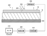
- the processing method of the wafer according to the embodiment includes a laser dicing apparatus 1 (see FIG. 1), a grinding apparatus 2 (see FIG. 3), and a transfer apparatus for transferring the wafer processed by the laser dicing apparatus 1 to the grinding apparatus 2 This process is performed by a processing device provided with a dividing device 200 (see FIG. 5) for dividing the wafer ground by the grinding device 2 into chips.
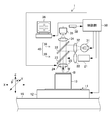
- FIG. 1 is a schematic view of the laser dicing apparatus 1. As shown to the same figure, the laser dicing apparatus 1 is comprised from the wafer moving part 11, the laser head 40, control part 50 grade
- the laser head 40 includes a laser optical unit 20 and an observation optical unit 30.
- the wafer moving unit 11 includes a suction stage 13 for holding the wafer W by suction, and an XYZ ⁇ table 12 provided on the main body base 16 of the laser dicing apparatus 1 for precisely moving the suction stage 13 in the XYZ ⁇ directions.
- the wafer moving unit 11 precisely moves the wafer W in the XYZ ⁇ direction of FIG.
- the wafer W In order to protect the surface (front surface) which is a device surface, the wafer W has a back grind tape B having a glue layer on its surface. Then, the wafer W is mounted on the suction stage 13 such that the back surface is upward.
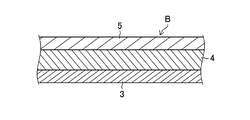
- FIG. 2 is a schematic cross-sectional view showing the configuration of the back grind tape B.
- the back grind tape B is a tape attached to the front surface of the wafer W when the back surface of the wafer W is processed.
- the back grind tape B is a tape of a three-layer structure in which the base film 3 as a base material, the intermediate absorption layer 4 with a thickness of 300 to 570 ⁇ m, and the above-mentioned paste layer 5 are laminated.
- the adhesive layer 5 is a necessary member because the back grind tape B is a highly adhesive tape unlike the protective film described above.
- the back grind tape B is attached to the wafer W in a state where the bumps BP are buried in the adhesive layer 5 (see FIG. 2) Therefore, the adhesion of the back grind tape B to the wafer W is increased by the anchor effect. As a result, the back grind tape B is difficult to separate from the wafer W, so the wafer W can be transported from the laser dicing apparatus 1 to the grinding apparatus 2 in a state where the surface of the wafer W is protected by the back grind tape B. The wafer W can be transferred from the device 2 to the dividing device 200 (see FIG. 5).
- the laser optical unit 20 shown in FIG. 1 includes a laser oscillator 21, a collimator lens 22, a half mirror 23, a condensing lens 24, and driving means 25 for minutely moving a laser beam parallel to a wafer W.
- the laser beam oscillated from the laser oscillator 21 is condensed on the inside of the wafer W through an optical system such as a collimator lens 22, a half mirror 23 and a condensing lens 24.
- the observation optical unit 30 includes an observation light source 31, a collimate lens 32, a half mirror 33, a condensing lens 34, a CCD (Charge Coupled Device) camera 35, an image processing unit 38, a television monitor 36, and the like.
- an observation light source 31 a collimate lens 32, a half mirror 33, a condensing lens 34, a CCD (Charge Coupled Device) camera 35, an image processing unit 38, a television monitor 36, and the like.
- CCD Charge Coupled Device
- the illumination light emitted from the observation light source 31 illuminates the back surface (upper surface) of the wafer W through the optical system such as the collimator lens 32, half mirror 33, and condenser lens 24. Reflected light from the back surface of the wafer W enters the CCD camera 35 via the condensing lens 24, the half mirrors 23 and 33, and the condensing lens 34. The surface image of the wafer W is captured by the CCD camera 35.
- the imaging data is input to the image processing unit 38 and used for alignment of the wafer W, and is also displayed on the television monitor 36 via the control unit 50.
- the control unit 50 includes a central processing unit (CPU), a memory, an input / output circuit unit and the like.
- the control unit 50 controls the operation of each unit of the laser dicing apparatus 1.
- the laser beam L emitted from the laser oscillator 21 is applied to the inside of the wafer W via an optical system such as a collimator lens 22, a half mirror 23 and a condensing lens 24.
- the Z-direction position of the condensing point of the laser beam L to be irradiated is accurately set at a predetermined position inside the wafer W by the Z-direction position adjustment of the wafer W by the XYZ ⁇ table 12 or the like.
- the XYZ ⁇ table 12 is processed and fed in the X direction which is the dicing direction, whereby one modified region is formed inside the wafer W along the cutting line of the wafer W.
- the XYZ ⁇ table 12 is indexed and fed in the Y direction by one pitch, and a reformed area is similarly formed in the next line.
- the modified region is formed along all the cutting lines parallel to the X direction, the XYZ ⁇ table 12 is rotated by 90 °, and all the modified regions are similarly formed on the cutting line orthogonal to the previous cutting line. Be done.
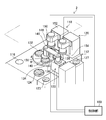
- FIG. 3 is a perspective view showing an outline configuration of the grinding device 2.
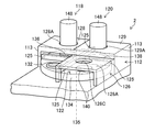
- An alignment stage 116, a rough grinding stage 118, a precision grinding stage 120, a polishing stage 122, a wafer cleaning stage 124, a polishing cloth cleaning stage 123, and a polishing cloth dressing stage 127 are provided on the main body 112 of the grinding apparatus 2.
- the grinding apparatus 2 is an apparatus that thins the thickness of the wafer W by processing the back surface of the wafer W in which the modified region is formed.
- the rough grinding stage 118, the fine grinding stage 120 and the polishing stage 122 are separated by a partition plate 125 (not shown in FIG. 3) as shown in FIG. 4 and the working fluid used in each of the stages 118, 120 and 122 is adjacent Scattering on the stage is prevented.
- the partition plate 125 is fixed to the index table 134 as shown in FIG.
- the partition plate 125 is formed in a cross shape so as to separate the four chucks 132, 136, 138, and 140 installed on the index table 134.
- the surface of the wafer W is held by suction on the chucks 132, 136, 138, 140 via the back grind tape B.
- the rough grinding stage 118 is a stage for rough grinding, and is surrounded by the side surface 113 of the main body 112, the top plate 128, and the partition plate 125.
- the fine grinding stage 120 is a stage for fine grinding, and is surrounded by the side surface 113 of the main body 112, the top plate 129, and the partition plate 125, similarly to the rough grinding stage 118.
- Through holes 128A and 129A are formed in the top plates 128 and 129, and the head of each stage is inserted through the through holes 128A and 129A.
- the polishing stage 122 shown in FIG. 3 performs chemical mechanical polishing and is covered by a casing 126 having a top plate 126A as shown in FIG. 4 in order to isolate it from other stages.
- a through hole 126C is formed in the top plate 126A, and the head of the polishing stage 122 is inserted through the through hole 126. Since the polishing stage 122 performs chemical mechanical polishing, the polishing fluid contains a chemical polishing agent.
- the back surface of the wafer W is polished by the polishing pad 156 and the slurry supplied from the polishing pad 156, and the damaged layer formed on the back surface of the wafer W is roughly polished and finely polished Removed by
- the processing-deteriorated layer is a generic term such as streaks and processing distortion (crystals are degraded) or the like generated by grinding.
- the alignment stage 116 is a stage which aligns the wafer W transferred from the laser dicing apparatus 1 by a transfer apparatus (not shown) at a predetermined position.
- the wafer W aligned by the alignment stage 116 is suctioned and held by a transfer robot (not shown), and then conveyed toward the empty chuck 132, and the back surface of the wafer W is backed to the suction surface of the chuck 132. It is held by suction via the grind tape B.
- the chuck 132 is placed on the index table 134. Further, chucks 136, 138, and 140 having the same function as the chuck 132 are installed at intervals of 90 degrees on the circumference centering on the rotation shaft 135 (see FIG. 4) of the index table 134. A spindle (not shown) of a motor (not shown) is connected to the rotating shaft 135.
- the chuck 136 is positioned on the rough grinding stage 118 in FIG. 3, and the chucked wafer W is rough ground here.
- the chuck 138 is positioned on the fine grinding stage 120 in FIG. 3, and the chucked wafer W is subjected to finish grinding (fine grinding, spark out) here.
- the chuck 140 is positioned on the polishing stage 122 in FIG. 3 and the chucked wafer W is polished here, and the processing-deteriorated layer produced by grinding and variations in the thickness of the wafer W are removed.
- the control unit 100 illustrated in FIG. 3 includes a CPU, a memory, an input / output circuit unit, and the like, and controls the operation of each unit of the grinding apparatus 2.
- the thickness of the wafer W held by suction by the chuck 132 is measured by a pair of measurement gauges (not shown) connected to the control unit 100.
- Each of these measurement gauges has a contact, the contact being in contact with the top surface (rear surface) of the wafer W, and the other contacts being in contact with the top surface of the chuck 132.
- These measurement gauges can detect the thickness of the wafer W as a difference between the readings of the in-process gauges with the upper surface of the chuck 132 as a reference point.
- the index table 134 is rotated by 90 degrees in the direction of arrow R in FIG. 3 by the control unit 100, so that the wafer W whose thickness is measured is positioned on the rough grinding stage 118, and the cup type grindstone 146 of the rough grinding stage 118 The back surface of W is roughly ground.
- the cup-shaped grindstone 146 is connected to an output shaft (not shown) of the motor 148 and attached to the grindstone feeder 152 via the support casing 150 of the motor 148.
- the grinding wheel feed device 152 moves the cup-shaped grinding wheel 146 up and down together with the motor 148.
- the cup-shaped grindstone 146 is pressed against the back surface of the wafer W by the downward movement of the grindstone feeder 152. Thereby, rough grinding of the back surface of the wafer W is performed.
- the control unit 100 sets the amount of downward movement of the cup-shaped grindstone 146 and controls the motor 148.
- the amount of descent movement of the cup-shaped grindstone 146 that is, the grinding amount by the cup-shaped grindstone 146 is set based on the reference position of the cup-shaped grindstone 146 registered in advance and the thickness of the wafer W detected by the measurement gauge. Ru. Further, the control unit 100 controls the number of rotations of the cup-shaped grinding wheel 146 by controlling the number of rotations of the motor 148.
- the thickness of the wafer W whose back surface is roughly ground in the rough grinding stage 118 is measured by a measurement gauge (not shown) connected to the control unit 100 after the cup-type grinding wheel 146 is moved away from the wafer W.
- the index table 134 is rotated by 90 degrees in the direction of arrow R in FIG. 3 by the control unit 100, so that the wafer W whose thickness is measured is positioned on the fine grinding stage 120, and the cup type grindstone 154 of the fine grinding stage 120 Grinded, sparked out. Since the structure of the fine grinding stage 120 is the same as the structure of the rough grinding stage 118, the description thereof is omitted here. Further, the grinding amount by the cup-shaped grindstone 154 is set by the control unit 100, and the processing movement amount and the rotation speed of the cup-shaped grindstone 154 are controlled by the control unit 100.
- the thickness of the wafer W whose back surface is finely ground by the precision grinding stage 120 is measured by a measurement gauge (not shown) connected to the control unit 100 after the cup-shaped grindstone 154 retreats from the wafer W.
- index table 134 is rotated 90 degrees in the direction of arrow R in FIG. 3 by control unit 100, wafer W whose thickness has been measured is positioned on polishing stage 122, and chemical mechanical polishing is performed by polishing cloth 156 of polishing stage 122. And the back surface of the wafer W is mirror-polished.
- the vertical movement distance of the polishing pad 156 is set by the control unit 100. Further, by controlling the motor 182 by the control unit 100, the position of the polishing pad 156 is controlled. Furthermore, the control unit 100 controls the number of rotations of the motor 158, that is, the number of rotations of the polishing pad 156.
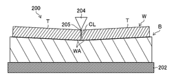
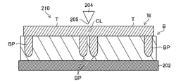
- FIG. 5 is a schematic structural view of the divider 200.
- the dividing apparatus 200 is an apparatus for dividing the wafer W along the cutting line by applying a load to the cutting line from the back side of the wafer W in a state where the back grind tape B is attached to the front surface of the wafer W .
- the wafer W is divided into individual chips T.
- the dividing device 200 includes a transparent rubber sheet 202 on which the front surface of the wafer W is placed via the back grind tape B, a break bar 204 on which the cutting line CL is pressed from the back surface (upper surface) of the wafer W, and a break bar.
- a lifting device 206 for moving the sheet 204 up and down relative to the sheet 202; an imaging device 208 for imaging the wafer W through the sheet 202; a display device 210 for displaying an image captured by the imaging device 208; And a control device 212 that controls the imaging device 208 and the like.
- the break bar 204 is longer than the length of the longest cutting line CL of the wafer W, and its tip is configured in a triangular shape in cross section, and as shown in FIG. Do. Thereby, the wafer W is divided along the cutting line CL because the pressing load by the break bar 204 is applied to the modified region.
- the division status of the wafer W is imaged by the imaging device 208 via the sheet 202. By displaying the image on the display device 210, the division situation of the wafer W is visually confirmed.
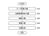
- FIG. 7 is a flowchart showing the process flow of the method of processing the wafer W.
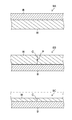
- FIG. 8 is an explanatory view showing a state of the wafer W corresponding to the flowchart of FIG.
- description will be made with reference to FIGS. 7 and 8.
- step S10 A back grind tape B is attached to the surface of the wafer W.
- the wafer W in which the back grind tape B was stuck on the surface is shown by the code 8A of FIG.
- Step S20 Modification Region Forming Step As shown in FIG. 1, the wafer W with the back grind tape B attached to the front surface is mounted on the suction stage 13 of the laser dicing apparatus 1 so that the back surface is upward. The following processing is performed by the laser dicing apparatus 1 and is controlled by the control unit 50.
- the laser beam L When the laser beam L is emitted from the laser oscillator 21, the laser beam L is irradiated to the inside of the wafer W via the optical system such as the collimator lens 22, the half mirror 23 and the condensing lens 24, and the inside of the wafer W is cut. A reformed region is formed along the line. A modified region P and a crack C formed in the thickness direction of the wafer W with the modified region P as a starting point are shown in a reference numeral 8B in FIG.
- the laser beam is irradiated from the surface (lower surface) of the wafer W to a depth (distance) of 60 ⁇ m to 80 ⁇ m. After the reformed regions P are formed along all the cutting lines, the process of step S20 is ended.
- step S30 After the modified regions are formed along all the cutting lines CL in the modified region forming step (step S20), the wafer W is transferred from the laser dicing apparatus 1 to the grinding apparatus 2 of FIG. 3 by the transfer apparatus (not shown). . The following processing is performed by the grinding device 2 and is controlled by the control unit 100.
- the transferred wafer W is placed on the chuck 132 (for example, the chucks 136, 138, and 140 can be used) with the back grind tape B attached to the front surface of the wafer W downward, and the front surface of the wafer W is back grind.
- the vacuum suction is made to the chuck 132 through the tape B.
- the index table 134 is rotated about the rotation shaft 135 to carry the chuck 132 onto the rough grinding stage 118, and the wafer W is roughly polished.
- Rough polishing is performed by rotating the chuck 132 and rotating the cup-shaped grinding wheel 146.
- Vitrified # 325 manufactured by Tokyo Seimitsu Co., Ltd. is used as the cup-shaped grindstone 146, and the rotation speed of the cup-shaped grindstone 146 is 3000 rpm.
- the index table 134 is rotated about the rotation shaft 135 to carry the chuck 132 onto the fine grinding stage 120, and the chuck 132 is rotated and the cup-shaped grindstone 154 is rotated to precisely polish the wafer W.
- Resin # 2000 manufactured by Tokyo Seimitsu Co., Ltd. is used as the cup-shaped grindstone 154, and the rotation speed of the cup-shaped grindstone 154 is 2400 rpm.
- grinding is performed to the target surface, that is, to a depth of 50 ⁇ m from the surface of the wafer W by rough polishing and fine polishing.
- 700 ⁇ m grinding is performed by rough polishing
- 30 to 40 ⁇ m grinding is performed by precise polishing, but it is not strictly set, and the grinding amount is set so that the time for rough polishing and precise polishing becomes the same. You may decide
- the reformed area on the back surface of the wafer W formed in the reformed area forming process can be removed in the grinding process.
- the modified region P by laser light does not remain in the chip cross section which is the final product. Therefore, the reforming layer can be broken from the cross section of the chip, and the chip can be prevented from being broken from the broken portion and dusting from the broken portion.
- step S40 The polishing process is performed by the grinding device 2 and is controlled by the control unit 100.
- reference numeral 8 ⁇ / b> C shows a wafer W whose rear surface is ground and polished to be mirror-finished.
- a polyurethane-impregnated non-woven cloth (for example, TS200L manufactured by Tokyo Seimitsu Co., Ltd.) is used as the polishing pad 156, colloidal silica is used as the slurry, and the rotation speed of the polishing pad 156 is 300 rpm.
- step S50 The dividing process is performed by the dividing device 200 of FIG. 5 and is controlled by the controller 212.
- the surface of the wafer W is placed on the sheet 202 via the backgrind tape B in a state where the backgrind tape B is attached to the surface of the wafer W first.
- the wafer W and the break bar 204 are relatively aligned so that the position of the first cutting line CL for cutting the wafer W and the position of the break bar 204 coincide in the vertical direction.
- the break bar 204 located at the retracted position from the back surface of the wafer W is moved down by the lifting device 206, and the top 205 of the break bar 204 presses the back surface of the wafer W.
- a load is applied to the crack C from the back surface of the wafer W, and the first cutting line CL is cut.
- the wafer W is cut along all the cutting lines, and the wafer W is divided into chips T.
- Contamination generated when the wafer W is divided adheres to the adhesive layer 5 (see FIG. 2) of the highly adhesive back grind tape B. Then, when the back grind tape B is peeled off from the surface of the wafer W, the contamination is removed from the wafer W while adhering to the adhesive layer 5 of the back grind tape B. As a result, it is possible to solve the problem of defective chips due to the contamination remaining on the wafer W.
- the back grind tape is directly applied to the front surface of the wafer W without peeling off the back grind tape B attached to the front surface of the wafer W for grinding the back surface of the wafer W
- a load is applied to the cutting line CL from the back surface of the wafer W to divide the wafer W along the cutting line, so that the processing process of the wafer can be simplified, and stable quality can be obtained. Chips can be obtained efficiently.
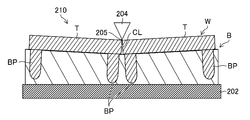
- the portion WA in the vicinity of the cutting line CL of the wafer W becomes the back grind tape B as shown in FIG.
- the wafer W is cut along the cutting line CL while gradually sinking, that is, while the chips T located on both sides of the cutting line CL are gradually inclined.
- the chip T inclines at a stretch and chipping occurs in the chip T There is.
- the bumps support the chip against the protective film up to a predetermined pressing load, the chip is pressed perpendicularly to the back surface of the wafer without bending stress being applied to the chip. Then, when the predetermined pressing load is exceeded, the bumps start to slide on the protective film, and the chips tilt at a stretch, resulting in an excessive opening between the chips. When such a phenomenon occurs, chipping easily occurs on the chip because the break bar 204 contacts the end of the chip or the adjacent chips collide with each other when the chip returns to the original position.
- bumps BP are formed on the surface of the wafer W for each chip T, and a back grind tape B is attached to the surface of the wafer W.
- the backgrind tape B is attached in a state where the bumps BP are buried in the adhesive layer 5 of the backgrind tape B.
- the adhesion between the wafer W (chip T) and the back grind tape B is enhanced by the anchor effect in which the bumps BP are buried in the adhesive layer 5. Therefore, as shown in FIG. 10, even if the break bar 204 is pressed against the back surface of the wafer W, the chip T can be further prevented from being inclined at a stretch. Therefore, even the wafer W of FIG. 9 on which the bumps BP are formed can be favorably divided.
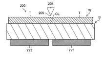
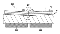
- FIG. 11 is a schematic structural view of a dividing device 220 according to another embodiment.
- the difference in configuration between the dividing device 220 and the dividing device 200 shown in FIG. 5 is that a pair of receiving plates 222, 222 is provided instead of the sheet 202, and the other configuration is the same as that of the dividing device 200. is there.
- the pair of receiving plates 222, 222 are spaced apart in the horizontal direction, and the cutting line CL of the wafer W is disposed therebetween.
- the surface of the wafer W is placed on the pair of receiving plates 222, 222 via the back grind tape B.
- the first cutting line CL to be cut is disposed between the pair of receiving plates 222, 222, and the position of the first cutting line CL and the position of the break bar 204 are relatively matched in the vertical direction.
- the break bar 204 is moved downward by the lift device 206 (see FIG. 5), and as shown in FIG. Press down. Thereby, a load is applied from the back surface of the wafer W to the modified region, and the cutting line CL is cut.
- Contamination generated at the time of dividing the wafer W adheres to the adhesive layer 5 (see FIG. 2) of the backgrind tape B having strong adhesive force, similarly to the dividing device 220 of FIG. Then, when the back grind tape B is peeled off from the surface of the wafer W, the contamination is removed from the wafer W while adhering to the adhesive layer 5 of the back grind tape B. Therefore, it is possible to solve the problem of defective chips due to the contamination remaining on the wafer W.
Landscapes
- Engineering & Computer Science (AREA)
- Physics & Mathematics (AREA)
- Condensed Matter Physics & Semiconductors (AREA)
- General Physics & Mathematics (AREA)
- Manufacturing & Machinery (AREA)
- Computer Hardware Design (AREA)
- Microelectronics & Electronic Packaging (AREA)
- Power Engineering (AREA)
- Optics & Photonics (AREA)
- Chemical Kinetics & Catalysis (AREA)
- General Chemical & Material Sciences (AREA)
- Oil, Petroleum & Natural Gas (AREA)
- Chemical & Material Sciences (AREA)
- Plasma & Fusion (AREA)
- Mechanical Engineering (AREA)
- Health & Medical Sciences (AREA)
- Toxicology (AREA)
- Mechanical Treatment Of Semiconductor (AREA)
- Dicing (AREA)
- Laser Beam Processing (AREA)
- Container, Conveyance, Adherence, Positioning, Of Wafer (AREA)
- Grinding Of Cylindrical And Plane Surfaces (AREA)
- Processing Of Stones Or Stones Resemblance Materials (AREA)
- Finish Polishing, Edge Sharpening, And Grinding By Specific Grinding Devices (AREA)
Priority Applications (3)
| Application Number | Priority Date | Filing Date | Title |
|---|---|---|---|
| KR1020207012050A KR20200049878A (ko) | 2017-11-06 | 2018-10-29 | 웨이퍼의 가공 방법 |
| KR1020207033283A KR102520523B1 (ko) | 2017-11-06 | 2018-10-29 | 웨이퍼의 가공 방법 |
| US16/867,126 US11075071B2 (en) | 2017-11-06 | 2020-05-05 | Method for processing wafer |
Applications Claiming Priority (2)
| Application Number | Priority Date | Filing Date | Title |
|---|---|---|---|
| JP2017213724A JP7157301B2 (ja) | 2017-11-06 | 2017-11-06 | ウェーハの加工方法 |
| JP2017-213724 | 2017-11-06 |
Related Child Applications (1)
| Application Number | Title | Priority Date | Filing Date |
|---|---|---|---|
| US16/867,126 Continuation US11075071B2 (en) | 2017-11-06 | 2020-05-05 | Method for processing wafer |
Publications (1)
| Publication Number | Publication Date |
|---|---|
| WO2019088011A1 true WO2019088011A1 (ja) | 2019-05-09 |
Family
ID=66331719
Family Applications (1)
| Application Number | Title | Priority Date | Filing Date |
|---|---|---|---|
| PCT/JP2018/040067 Ceased WO2019088011A1 (ja) | 2017-11-06 | 2018-10-29 | ウェーハの加工方法 |
Country Status (4)
| Country | Link |
|---|---|
| US (1) | US11075071B2 (enExample) |
| JP (2) | JP7157301B2 (enExample) |
| KR (2) | KR102520523B1 (enExample) |
| WO (1) | WO2019088011A1 (enExample) |
Families Citing this family (2)
| Publication number | Priority date | Publication date | Assignee | Title |
|---|---|---|---|---|
| JP7460386B2 (ja) * | 2020-02-14 | 2024-04-02 | 株式会社ディスコ | 被加工物の加工方法 |
| JP2023128800A (ja) * | 2022-03-04 | 2023-09-14 | 株式会社ディスコ | 分割装置 |
Citations (3)
| Publication number | Priority date | Publication date | Assignee | Title |
|---|---|---|---|---|
| JP2013004583A (ja) * | 2011-06-13 | 2013-01-07 | Tokyo Seimitsu Co Ltd | 半導体基板の切断方法及び半導体基板の切断装置 |
| JP2014165462A (ja) * | 2013-02-27 | 2014-09-08 | Lintec Corp | 半導体チップの製造方法 |
| JP2017017163A (ja) * | 2015-06-30 | 2017-01-19 | 日亜化学工業株式会社 | 半導体素子の製造方法 |
Family Cites Families (24)
| Publication number | Priority date | Publication date | Assignee | Title |
|---|---|---|---|---|
| JP3832353B2 (ja) | 2002-02-15 | 2006-10-11 | 松下電器産業株式会社 | 半導体装置の製造方法 |
| TWI326626B (en) * | 2002-03-12 | 2010-07-01 | Hamamatsu Photonics Kk | Laser processing method |
| JP3624909B2 (ja) | 2002-03-12 | 2005-03-02 | 浜松ホトニクス株式会社 | レーザ加工方法 |
| US7241642B2 (en) * | 2004-01-30 | 2007-07-10 | Intel Corporation | Mounting and dicing process for wafers |
| JP2007235068A (ja) * | 2006-03-03 | 2007-09-13 | Tokyo Seimitsu Co Ltd | ウェーハ加工方法 |
| JP5197037B2 (ja) | 2008-01-30 | 2013-05-15 | 株式会社東京精密 | バンプが形成されたウェーハを処理するウェーハ処理方法 |
| JP2011054827A (ja) * | 2009-09-03 | 2011-03-17 | Fujitsu Semiconductor Ltd | 半導体装置の製造方法及び表面保護テープ |
| JP2012104644A (ja) | 2010-11-10 | 2012-05-31 | Tokyo Seimitsu Co Ltd | ウェーハ破断方法およびウェーハ破断装置 |
| JP5824365B2 (ja) | 2012-01-16 | 2015-11-25 | 三星ダイヤモンド工業株式会社 | 脆性材料基板のブレイク方法 |
| JP6061590B2 (ja) | 2012-09-27 | 2017-01-18 | 株式会社ディスコ | 表面保護部材および加工方法 |
| JP6059499B2 (ja) * | 2012-10-05 | 2017-01-11 | リンテック株式会社 | 表面保護シート |
| US9230862B2 (en) * | 2013-05-14 | 2016-01-05 | Texas Instruments Incorporated | Wafer die separation |
| JP5637329B1 (ja) * | 2013-07-01 | 2014-12-10 | 富士ゼロックス株式会社 | 半導体片の製造方法、半導体片を含む回路基板および画像形成装置 |
| JP6185792B2 (ja) * | 2013-08-29 | 2017-08-23 | 三星ダイヤモンド工業株式会社 | 半導体ウエハの分断方法 |
| JP6119551B2 (ja) | 2013-10-16 | 2017-04-26 | 三星ダイヤモンド工業株式会社 | 弾性支持板、破断装置及び分断方法 |
| JP6119550B2 (ja) | 2013-10-16 | 2017-04-26 | 三星ダイヤモンド工業株式会社 | エキスパンダ、破断装置及び分断方法 |
| JP2016040079A (ja) | 2014-08-12 | 2016-03-24 | 三星ダイヤモンド工業株式会社 | 脆性材料基板の分断方法及び分断装置 |
| JP6517588B2 (ja) | 2015-05-27 | 2019-05-22 | デクセリアルズ株式会社 | 熱硬化性接着シート、及び半導体装置の製造方法 |
| JP6657515B2 (ja) | 2015-08-31 | 2020-03-04 | 株式会社ディスコ | ウェーハを処理する方法および該方法で使用するための保護シート |
| JP2017079291A (ja) * | 2015-10-21 | 2017-04-27 | 株式会社ディスコ | ウエーハの加工方法 |
| JP6574688B2 (ja) | 2015-11-19 | 2019-09-11 | 日東電工株式会社 | シート状樹脂組成物、積層シート及び半導体装置の製造方法 |
| JP6721325B2 (ja) | 2015-12-14 | 2020-07-15 | デクセリアルズ株式会社 | 熱硬化性接着シート、及び半導体装置の製造方法 |
| JP6621338B2 (ja) | 2016-02-09 | 2019-12-18 | 株式会社ディスコ | 被加工物の樹脂被覆方法及び被加工物の加工方法 |
| US10453764B2 (en) * | 2016-08-11 | 2019-10-22 | Advanced Semiconductor Engineering, Inc. | Molding for large panel fan-out package |
-
2017
- 2017-11-06 JP JP2017213724A patent/JP7157301B2/ja active Active
-
2018
- 2018-10-29 WO PCT/JP2018/040067 patent/WO2019088011A1/ja not_active Ceased
- 2018-10-29 KR KR1020207033283A patent/KR102520523B1/ko active Active
- 2018-10-29 KR KR1020207012050A patent/KR20200049878A/ko not_active Ceased
-
2020
- 2020-05-05 US US16/867,126 patent/US11075071B2/en active Active
-
2022
- 2022-08-05 JP JP2022125778A patent/JP2022172109A/ja active Pending
Patent Citations (3)
| Publication number | Priority date | Publication date | Assignee | Title |
|---|---|---|---|---|
| JP2013004583A (ja) * | 2011-06-13 | 2013-01-07 | Tokyo Seimitsu Co Ltd | 半導体基板の切断方法及び半導体基板の切断装置 |
| JP2014165462A (ja) * | 2013-02-27 | 2014-09-08 | Lintec Corp | 半導体チップの製造方法 |
| JP2017017163A (ja) * | 2015-06-30 | 2017-01-19 | 日亜化学工業株式会社 | 半導体素子の製造方法 |
Also Published As
| Publication number | Publication date |
|---|---|
| KR20200133022A (ko) | 2020-11-25 |
| KR20200049878A (ko) | 2020-05-08 |
| JP2022172109A (ja) | 2022-11-15 |
| JP2019087604A (ja) | 2019-06-06 |
| US11075071B2 (en) | 2021-07-27 |
| KR102520523B1 (ko) | 2023-04-12 |
| JP7157301B2 (ja) | 2022-10-20 |
| US20200266047A1 (en) | 2020-08-20 |
Similar Documents
| Publication | Publication Date | Title |
|---|---|---|
| CN101604659B (zh) | 光器件晶片的分割方法 | |
| JP4733934B2 (ja) | ウエーハの加工方法 | |
| JP5707889B2 (ja) | 半導体基板の切断方法及び半導体基板の切断装置 | |
| US9640420B2 (en) | Wafer processing method | |
| TWI469200B (zh) | Processing method of optical element wafers (3) | |
| KR102574672B1 (ko) | 피가공물의 가공 방법 | |
| WO2007099986A1 (ja) | ウェーハ加工方法 | |
| JP2009206162A (ja) | ウエーハの分割方法 | |
| KR20160072775A (ko) | 웨이퍼의 가공 방법 | |
| WO2007091670A1 (ja) | ウェーハ加工装置及び方法 | |
| US20240128087A1 (en) | Wafer processing method | |
| WO2007099787A1 (ja) | ウェーハ加工方法 | |
| KR20170030035A (ko) | 웨이퍼의 가공 방법 | |
| CN110875173A (zh) | SiC基板的加工方法 | |
| KR20180005604A (ko) | 반도체 디바이스 칩의 제조 방법 | |
| JP2011091293A (ja) | ウエーハの加工方法 | |
| JP2017028160A (ja) | ウエーハの加工方法 | |
| JP2011049431A (ja) | ウエーハの加工方法 | |
| CN100428418C (zh) | 晶片的分割方法 | |
| JP2022172109A (ja) | ウェーハの加工方法 | |
| JP2014053358A (ja) | ウエーハの加工方法 | |
| JP2005228794A (ja) | チップ製造方法 | |
| JP5939769B2 (ja) | 板状物の加工方法 | |
| JP4402974B2 (ja) | ウエーハの分割方法 | |
| JP2011151070A (ja) | ウエーハの加工方法 |
Legal Events
| Date | Code | Title | Description |
|---|---|---|---|
| 121 | Ep: the epo has been informed by wipo that ep was designated in this application |
Ref document number: 18872888 Country of ref document: EP Kind code of ref document: A1 |
|
| ENP | Entry into the national phase |
Ref document number: 20207012050 Country of ref document: KR Kind code of ref document: A |
|
| NENP | Non-entry into the national phase |
Ref country code: DE |
|
| 122 | Ep: pct application non-entry in european phase |
Ref document number: 18872888 Country of ref document: EP Kind code of ref document: A1 |