WO2019064904A1 - 半導体モジュール - Google Patents
半導体モジュール Download PDFInfo
- Publication number
- WO2019064904A1 WO2019064904A1 PCT/JP2018/028790 JP2018028790W WO2019064904A1 WO 2019064904 A1 WO2019064904 A1 WO 2019064904A1 JP 2018028790 W JP2018028790 W JP 2018028790W WO 2019064904 A1 WO2019064904 A1 WO 2019064904A1
- Authority
- WO
- WIPO (PCT)
- Prior art keywords
- terminal
- electrode side
- bus bar
- negative electrode
- positive electrode
- Prior art date
- Legal status (The legal status is an assumption and is not a legal conclusion. Google has not performed a legal analysis and makes no representation as to the accuracy of the status listed.)
- Ceased
Links
Images


Classifications
-
- H—ELECTRICITY
- H02—GENERATION; CONVERSION OR DISTRIBUTION OF ELECTRIC POWER
- H02M—APPARATUS FOR CONVERSION BETWEEN AC AND AC, BETWEEN AC AND DC, OR BETWEEN DC AND DC, AND FOR USE WITH MAINS OR SIMILAR POWER SUPPLY SYSTEMS; CONVERSION OF DC OR AC INPUT POWER INTO SURGE OUTPUT POWER; CONTROL OR REGULATION THEREOF
- H02M7/00—Conversion of AC power input into DC power output; Conversion of DC power input into AC power output
- H02M7/003—Constructional details, e.g. physical layout, assembly, wiring or busbar connections
-
- H—ELECTRICITY
- H01—ELECTRIC ELEMENTS
- H01L—SEMICONDUCTOR DEVICES NOT COVERED BY CLASS H10
- H01L23/00—Details of semiconductor or other solid state devices
- H01L23/48—Arrangements for conducting electric current to or from the solid state body in operation, e.g. leads, terminal arrangements ; Selection of materials therefor
- H01L23/50—Arrangements for conducting electric current to or from the solid state body in operation, e.g. leads, terminal arrangements ; Selection of materials therefor for integrated circuit devices, e.g. power bus, number of leads
-
- H—ELECTRICITY
- H01—ELECTRIC ELEMENTS
- H01L—SEMICONDUCTOR DEVICES NOT COVERED BY CLASS H10
- H01L23/00—Details of semiconductor or other solid state devices
- H01L23/52—Arrangements for conducting electric current within the device in operation from one component to another, i.e. interconnections, e.g. wires, lead frames
-
- H—ELECTRICITY
- H01—ELECTRIC ELEMENTS
- H01L—SEMICONDUCTOR DEVICES NOT COVERED BY CLASS H10
- H01L25/00—Assemblies consisting of a plurality of semiconductor or other solid state devices
- H01L25/03—Assemblies consisting of a plurality of semiconductor or other solid state devices all the devices being of a type provided for in a single subclass of subclasses H10B, H10D, H10F, H10H, H10K or H10N, e.g. assemblies of rectifier diodes
- H01L25/04—Assemblies consisting of a plurality of semiconductor or other solid state devices all the devices being of a type provided for in a single subclass of subclasses H10B, H10D, H10F, H10H, H10K or H10N, e.g. assemblies of rectifier diodes the devices not having separate containers
- H01L25/07—Assemblies consisting of a plurality of semiconductor or other solid state devices all the devices being of a type provided for in a single subclass of subclasses H10B, H10D, H10F, H10H, H10K or H10N, e.g. assemblies of rectifier diodes the devices not having separate containers the devices being of a type provided for in group subclass H10D
-
- H—ELECTRICITY
- H01—ELECTRIC ELEMENTS
- H01L—SEMICONDUCTOR DEVICES NOT COVERED BY CLASS H10
- H01L25/00—Assemblies consisting of a plurality of semiconductor or other solid state devices
- H01L25/03—Assemblies consisting of a plurality of semiconductor or other solid state devices all the devices being of a type provided for in a single subclass of subclasses H10B, H10D, H10F, H10H, H10K or H10N, e.g. assemblies of rectifier diodes
- H01L25/10—Assemblies consisting of a plurality of semiconductor or other solid state devices all the devices being of a type provided for in a single subclass of subclasses H10B, H10D, H10F, H10H, H10K or H10N, e.g. assemblies of rectifier diodes the devices having separate containers
- H01L25/11—Assemblies consisting of a plurality of semiconductor or other solid state devices all the devices being of a type provided for in a single subclass of subclasses H10B, H10D, H10F, H10H, H10K or H10N, e.g. assemblies of rectifier diodes the devices having separate containers the devices being of a type provided for in subclass H10D
-
- H—ELECTRICITY
- H01—ELECTRIC ELEMENTS
- H01L—SEMICONDUCTOR DEVICES NOT COVERED BY CLASS H10
- H01L25/00—Assemblies consisting of a plurality of semiconductor or other solid state devices
- H01L25/18—Assemblies consisting of a plurality of semiconductor or other solid state devices the devices being of the types provided for in two or more different main groups of the same subclass of H10B, H10D, H10F, H10H, H10K or H10N
-
- H—ELECTRICITY
- H04—ELECTRIC COMMUNICATION TECHNIQUE
- H04N—PICTORIAL COMMUNICATION, e.g. TELEVISION
- H04N23/00—Cameras or camera modules comprising electronic image sensors; Control thereof
- H04N23/60—Control of cameras or camera modules
- H04N23/66—Remote control of cameras or camera parts, e.g. by remote control devices
- H04N23/661—Transmitting camera control signals through networks, e.g. control via the Internet
-
- H—ELECTRICITY
- H04—ELECTRIC COMMUNICATION TECHNIQUE
- H04N—PICTORIAL COMMUNICATION, e.g. TELEVISION
- H04N23/00—Cameras or camera modules comprising electronic image sensors; Control thereof
- H04N23/90—Arrangement of cameras or camera modules, e.g. multiple cameras in TV studios or sports stadiums
-
- H—ELECTRICITY
- H10—SEMICONDUCTOR DEVICES; ELECTRIC SOLID-STATE DEVICES NOT OTHERWISE PROVIDED FOR
- H10D—INORGANIC ELECTRIC SEMICONDUCTOR DEVICES
- H10D12/00—Bipolar devices controlled by the field effect, e.g. insulated-gate bipolar transistors [IGBT]
- H10D12/01—Manufacture or treatment
-
- H—ELECTRICITY
- H10—SEMICONDUCTOR DEVICES; ELECTRIC SOLID-STATE DEVICES NOT OTHERWISE PROVIDED FOR
- H10D—INORGANIC ELECTRIC SEMICONDUCTOR DEVICES
- H10D84/00—Integrated devices formed in or on semiconductor substrates that comprise only semiconducting layers, e.g. on Si wafers or on GaAs-on-Si wafers
- H10D84/40—Integrated devices formed in or on semiconductor substrates that comprise only semiconducting layers, e.g. on Si wafers or on GaAs-on-Si wafers characterised by the integration of at least one component covered by groups H10D12/00 or H10D30/00 with at least one component covered by groups H10D10/00 or H10D18/00, e.g. integration of IGFETs with BJTs
- H10D84/401—Combinations of FETs or IGBTs with BJTs
- H10D84/403—Combinations of FETs or IGBTs with BJTs and with one or more of diodes, resistors or capacitors
-
- H—ELECTRICITY
- H01—ELECTRIC ELEMENTS
- H01L—SEMICONDUCTOR DEVICES NOT COVERED BY CLASS H10
- H01L2224/00—Indexing scheme for arrangements for connecting or disconnecting semiconductor or solid-state bodies and methods related thereto as covered by H01L24/00
- H01L2224/01—Means for bonding being attached to, or being formed on, the surface to be connected, e.g. chip-to-package, die-attach, "first-level" interconnects; Manufacturing methods related thereto
- H01L2224/26—Layer connectors, e.g. plate connectors, solder or adhesive layers; Manufacturing methods related thereto
- H01L2224/31—Structure, shape, material or disposition of the layer connectors after the connecting process
- H01L2224/32—Structure, shape, material or disposition of the layer connectors after the connecting process of an individual layer connector
- H01L2224/321—Disposition
- H01L2224/32151—Disposition the layer connector connecting between a semiconductor or solid-state body and an item not being a semiconductor or solid-state body, e.g. chip-to-substrate, chip-to-passive
- H01L2224/32221—Disposition the layer connector connecting between a semiconductor or solid-state body and an item not being a semiconductor or solid-state body, e.g. chip-to-substrate, chip-to-passive the body and the item being stacked
- H01L2224/32245—Disposition the layer connector connecting between a semiconductor or solid-state body and an item not being a semiconductor or solid-state body, e.g. chip-to-substrate, chip-to-passive the body and the item being stacked the item being metallic
-
- H—ELECTRICITY
- H01—ELECTRIC ELEMENTS
- H01L—SEMICONDUCTOR DEVICES NOT COVERED BY CLASS H10
- H01L2224/00—Indexing scheme for arrangements for connecting or disconnecting semiconductor or solid-state bodies and methods related thereto as covered by H01L24/00
- H01L2224/01—Means for bonding being attached to, or being formed on, the surface to be connected, e.g. chip-to-package, die-attach, "first-level" interconnects; Manufacturing methods related thereto
- H01L2224/34—Strap connectors, e.g. copper straps for grounding power devices; Manufacturing methods related thereto
- H01L2224/39—Structure, shape, material or disposition of the strap connectors after the connecting process
- H01L2224/40—Structure, shape, material or disposition of the strap connectors after the connecting process of an individual strap connector
- H01L2224/401—Disposition
- H01L2224/40151—Connecting between a semiconductor or solid-state body and an item not being a semiconductor or solid-state body, e.g. chip-to-substrate, chip-to-passive
- H01L2224/40221—Connecting between a semiconductor or solid-state body and an item not being a semiconductor or solid-state body, e.g. chip-to-substrate, chip-to-passive the body and the item being stacked
- H01L2224/40245—Connecting between a semiconductor or solid-state body and an item not being a semiconductor or solid-state body, e.g. chip-to-substrate, chip-to-passive the body and the item being stacked the item being metallic
-
- H—ELECTRICITY
- H01—ELECTRIC ELEMENTS
- H01L—SEMICONDUCTOR DEVICES NOT COVERED BY CLASS H10
- H01L2924/00—Indexing scheme for arrangements or methods for connecting or disconnecting semiconductor or solid-state bodies as covered by H01L24/00
- H01L2924/10—Details of semiconductor or other solid state devices to be connected
- H01L2924/11—Device type
- H01L2924/13—Discrete devices, e.g. 3 terminal devices
- H01L2924/1304—Transistor
- H01L2924/1305—Bipolar Junction Transistor [BJT]
- H01L2924/13055—Insulated gate bipolar transistor [IGBT]
-
- H—ELECTRICITY
- H01—ELECTRIC ELEMENTS
- H01L—SEMICONDUCTOR DEVICES NOT COVERED BY CLASS H10
- H01L2924/00—Indexing scheme for arrangements or methods for connecting or disconnecting semiconductor or solid-state bodies as covered by H01L24/00
- H01L2924/15—Details of package parts other than the semiconductor or other solid state devices to be connected
- H01L2924/181—Encapsulation
-
- H—ELECTRICITY
- H01—ELECTRIC ELEMENTS
- H01L—SEMICONDUCTOR DEVICES NOT COVERED BY CLASS H10
- H01L2924/00—Indexing scheme for arrangements or methods for connecting or disconnecting semiconductor or solid-state bodies as covered by H01L24/00
- H01L2924/30—Technical effects
- H01L2924/301—Electrical effects
- H01L2924/30107—Inductance
Definitions
- the present disclosure relates to a semiconductor module.
- Patent Document 1 discloses a semiconductor module.
- a semiconductor module a plurality of semiconductor elements (IGBT elements) constituting upper and lower arms are sealed by a sealing resin body (resin portion).
- the positive electrode side terminal (high potential power supply terminal), the negative electrode side terminal (low potential power supply terminal), and the output terminal protrude from the same surface of the sealing resin body.
- the protruding portions of the respective terminals are arranged in the order of the positive electrode side terminal, the negative electrode side terminal and the output terminal.
- the positive electrode terminal and the negative electrode terminal which are power supply terminals, are connected to, for example, a smoothing capacitor via a bus bar.
- a positive bus bar connected to the positive terminal and a negative bus bar connected to the negative terminal are extended in the direction in which the terminals are arranged.
- the projection length of the positive electrode side terminal disposed at one end in the alignment direction is longer than the projection length of the negative electrode side terminal disposed in the middle. For this reason, it is necessary to bypass the positive electrode side terminal and connect the negative electrode side bus bar to the negative electrode side terminal, and the parasitic inductance and hence the surge voltage become large.
- An object of the present disclosure is to provide a semiconductor module capable of reducing a surge voltage.
- the semiconductor module is A plurality of semiconductor elements constituting upper and lower arms; A sealing resin body for sealing a plurality of semiconductor elements; A power supply terminal having a positive electrode side terminal connected to any of the plurality of semiconductor elements and protruding from the sealing resin body, and a negative electrode side terminal connected to any of the plurality of semiconductor elements and protruding from the sealing resin body; An output terminal connected to any one of the plurality of semiconductor elements and protruding from the sealing resin body; The positive electrode side terminal, the negative electrode side terminal, and the output terminal protrude from the same surface of the sealing resin body, and the protruding portions are arranged side by side so that the output terminal is arranged at one end, The protruding length of the power supply terminal arranged at the end opposite to the output terminal is shorter than the protruding length of the power supply terminal arranged at the middle.
- the bus bar connected to the middle power supply terminal can be arranged in the arranging direction without arranging so as to avoid the power supply terminal at the end. It can be extended.
- the bypass of the bus bar can be suppressed, the parasitic inductance can be reduced.
- the suppression of the detour enables opposing arrangement of the bus bar connected to the positive electrode side terminal and the bus bar connected to the negative electrode side terminal, which also reduces parasitic inductance.
- the surge voltage can be reduced.
- FIG. 4 is a cross-sectional view taken along the line IV-IV of FIG. It is a top view which shows a comparative example. It is a top view which shows the semiconductor module of 2nd Embodiment. It is a top view which shows a modification. It is a top view which shows the semiconductor module of 3rd Embodiment. It is a top view which shows the semiconductor module of 4th Embodiment. It is a top view which shows the semiconductor module of 5th Embodiment. It is a top view of the semiconductor module seen from the XI direction.
- the thickness direction of the semiconductor element is orthogonal to the Z direction and the Z direction, and the arrangement direction of the power supply terminal and the output terminal is referred to as the X direction.
- a direction orthogonal to both the Z direction and the X direction is referred to as a Y direction.
- the shape when viewed in the XY plane is a plane shape.
- XY plane view can be said to be projection view in the Z direction.
- H at the end of the code indicates that it is an element on the upper arm side of the upper and lower arms
- L at the end indicates that it is an element on the lower arm side.
- H and L are given to some of the elements at the end, and for the other part, the upper arm and the lower arm have a common code.
- Power converter 1 shown in FIG. 1 is mounted on, for example, an electric car or a hybrid car.
- the power conversion device 1 is configured to convert a DC voltage supplied from a DC power supply 2 mounted on a vehicle into a three-phase alternating current and output the same to a three-phase alternating current motor 3.
- the motor 3 functions as a travel drive source of the vehicle.
- the power conversion device 1 can also convert the power generated by the motor 3 into direct current and charge the direct current power supply 2.
- the power conversion device 1 is capable of bi-directional power conversion.
- the power converter 1 includes a smoothing capacitor 4 and an inverter 5.
- a terminal on the positive electrode side of the smoothing capacitor 4 is connected to a positive electrode that is an electrode on the high potential side of the DC power supply 2, and a terminal on the negative electrode side is connected to a negative electrode that is an electrode on the low potential side of the DC power supply 2.
- the inverter 5 converts the input DC power into a three-phase AC of a predetermined frequency, and outputs it to the motor 3.
- the inverter 5 converts alternating current power generated by the motor 3 into direct current power.
- the inverter 5 consists of six arms.
- the inverter 5 is composed of upper and lower arms for three phases.
- the upper and lower arms of each phase are formed by connecting two arms in series between the positive electrode side line 6 which is a power supply line on the positive electrode side and the negative electrode side line 7 which is a power supply line on the negative electrode side.
- the positive electrode side line 6 is also referred to as a high potential power supply line
- the negative electrode side line 7 is also referred to as a low potential power supply line.
- the connection point between the upper arm and the lower arm is connected to the output line 8 to the motor 3.
- an insulated gate bipolar transistor (hereinafter referred to as an IGBT) is employed as a semiconductor element constituting each arm.
- the semiconductor module 10 includes two IGBTs 11H and 11L connected in series.
- the feedback diodes FWD 12 H and 12 L are connected in reverse parallel to the IGBTs 11 H and 11 L, respectively.
- the upper and lower arms are configured to include the two IGBTs 11H and 11L.
- Reference numeral 11g shown in FIG. 1 denotes gate electrodes of the IGBTs 11H and 11L.
- the semiconductor element has the gate electrode 11g.
- n channel type is adopted as IGBT11H and 11L.
- the collector electrode 11 c of the IGBT 11 H constituting the upper arm is electrically connected to the positive electrode side line 6.
- the emitter electrode 11e of the IGBT 11L constituting the lower arm is electrically connected to the negative electrode side line 7.
- the emitter electrode 11e of the IGBT 11H on the upper arm side and the collector electrode 11c of the IGBT 11L on the lower arm side are connected to each other.
- the power conversion device 1 controls the operation of a boost converter that boosts the DC voltage supplied from the DC power supply 2, the inverter 5, and the semiconductor elements that constitute the boost converter.
- a circuit or the like may be provided.
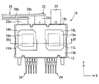
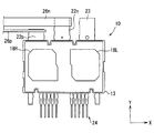
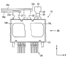
- the semiconductor module 10 includes the IGBTs 11H and 11L, the sealing resin body 13, the first heat sinks 14H and 14L, the terminal 16, the second heat sinks 18H and 18L, the joint portion 20, the power supply terminal 22, An output terminal 23 and a signal terminal 24 are provided.
- the semiconductor module 10 of the present embodiment further includes a bus bar 26.
- the IGBTs 11H and 11L as semiconductor elements are configured on a semiconductor substrate (semiconductor chip) such as silicon or silicon carbide.
- the IGBTs 11H and 11L are both n-channel type.
- the FWDs 12H and 12L are also integrally formed on the IGBTs 11H and 11L. Specifically, the FWD 12H is formed in the IGBT 11H, and the FWD 12L is formed in the IGBT 11L.
- RC (Reverse Conducting) -IGBT is adopted as the IGBTs 11H and 11L.
- the IGBTs 11H and 11L have a vertical structure so that current flows in the Z direction.
- the gate electrodes 11g described above are also formed on the IGBTs 11H and 11L, respectively.
- the gate electrode 11g has a trench structure.
- the collector electrode 11c is formed on one surface of the IGBTs 11H and 11L, and the emitter electrode 11e is formed on the back surface opposite to the one surface.
- the collector electrode 11c doubles as a cathode electrode of the FWDs 12H and 12L, and the emitter electrode 11e doubles as an anode electrode of the FWDs 12H and 12L.
- the IGBTs 11H and 11L have substantially the same planar shape, specifically, a substantially rectangular planar shape, and have substantially the same thickness and approximately the same thickness.
- the IGBTs 11H and 11L have the same configuration.
- the IGBTs 11H and 11L are arranged such that their collector electrodes 11c are on the same side in the Z direction, and their emitter electrodes 11e are on the same side in the Z direction.
- the IGBTs 11H and 11L are located substantially at the same height in the Z direction, and are arranged side by side in the X direction.
- pads serving as signal electrodes are formed on the back surfaces of the IGBTs 11H and 11L, that is, the emitter electrode formation surfaces.
- the pad is formed at a position different from that of the emitter electrode 11e.
- the pad is electrically separated from the emitter electrode 11e.
- the pad is formed at the end opposite to the region where the emitter electrode 11e is formed in the Y direction.
- each of the IGBTs 11H and 11L has five pads. Specifically, five pads for the gate electrode, Kelvin emitter for detecting the potential of the emitter electrode 11 e, for current sensing, for the anode potential of the temperature sensor (temperature sensitive diode) for detecting the temperature of the IGBTs 11 H and 11 L It has a potential.
- the five pads are collectively formed on one end side in the Y direction in the planar substantially rectangular IGBTs 11H and 11L, and are formed side by side in the X direction.
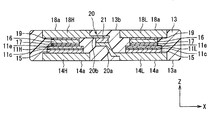
- the sealing resin body 13 seals the IGBTs 11H and 11L.
- Sealing resin body 13 is made of, for example, an epoxy resin.
- Sealing resin body 13 is formed by, for example, a transfer molding method.
- the sealing resin body 13 has a surface 13a orthogonal to the Z direction, a back surface 13b opposite to the surface 13a, and a side surface connecting the surface 13a and the back surface 13b.
- the one surface 13a and the back surface 13b are, for example, flat surfaces.
- the first heat sinks 14H and 14L perform the function of radiating the heat of the corresponding IGBTs 11H and 11L to the outside of the semiconductor module 10, and also perform the function of wiring. For this reason, in order to ensure heat conductivity and electrical conductivity, it is formed using at least a metal material.
- the first heat sinks 14H and 14L are provided so as to include the corresponding IGBTs 11H and 11L in the projection view from the Z direction.
- the first heat sinks 14H and 14L are disposed on one surface 13a side of the sealing resin body 13 with respect to the corresponding IGBTs 11H and 11L.
- the first heat sinks 14H and 14L are connected to the corresponding collector electrodes 11c of the IGBTs 11H and 11L via the solder 15. Most part of each of the first heat sinks 14H and 14L is covered by the sealing resin body 13. Of the surfaces of the first heat sinks 14H and 14L, the heat radiation surface 14a opposite to the IGBTs 11H and 11L is exposed from the sealing resin body 13. The heat dissipation surface 14a is substantially flush with the one surface 13a. Of the surfaces of the first heat sinks 14H and 14L, the portion excluding the connection portion with the solder 15 and the heat radiation surface 14a is covered with the sealing resin body 13.
- the collector electrode 11 c of the IGBT 11 H is connected to the surface of the first heat sink 14 H opposite to the heat dissipation surface 14 a through the solder 15.
- the collector electrode 11 c of the IGBT 11 L is connected to the surface of the first heat sink 14 L opposite to the heat radiation surface 14 a via the solder 15.
- the first heat sinks 14H and 14L are arranged side by side in the X direction and arranged at substantially the same position in the Z direction.
- the heat radiation surfaces 14 a of the first heat sinks 14 H and 14 L are exposed from the one surface 13 a of the sealing resin body 13 and are aligned with each other in the X direction.
- the terminal 16 is interposed between the corresponding IGBTs 11H and 11L and the second heat sinks 18H and 18L.
- the terminal 16 is formed using at least a metal material in order to ensure thermal conductivity and electrical conductivity because it is located on the way of thermal conductivity and electrical conduction path between the IGBTs 11H and 11L and the second heat sinks 18H and 18L. There is.
- the terminal 16 is disposed opposite to the emitter electrode 11 e and connected to the emitter electrode 11 e via the solder 17.
- the terminal 16 is provided for each of the IGBTs 11H and 11L.
- the second heat sinks 18H and 18L not only function to radiate the heat of the corresponding IGBTs 11H and 11L to the outside of the semiconductor module 10, but also function as wiring.
- the second heat sinks 18H and 18L are provided so as to include the corresponding IGBTs 11H and 11L in the projection view from the Z direction.
- the second heat sinks 18H and 18L are disposed on the back surface 13b side of the sealing resin body 13 with respect to the corresponding IGBTs 11H and 11L in the Z direction.
- the second heat sinks 18H and 18L are electrically connected to the emitter electrodes 11e of the corresponding IGBTs 11H and 11L. Specifically, the second heat sinks 18 H and 18 L are electrically connected to the corresponding emitter electrodes 11 e via the solder 17, the terminal 16 and the solder 19. Most part of the second heat sinks 18H and 18L is covered by the sealing resin body 13. Of the surfaces of the second heat sinks 18H and 18L, the heat release surface 18a opposite to the IGBTs 11H and 11L is exposed from the sealing resin body 13. The heat radiation surface 18a is substantially flush with the back surface 13b. Of the surfaces of the second heat sinks 18H and 18L, the portions other than the connection portions with the solder 19 and the heat radiation surface 18a are covered with the sealing resin body 13.
- the terminal 16 corresponding to the IGBT 11H is connected to the surface of the second heat sink 18H opposite to the heat dissipation surface 18a through the solder 19.
- a terminal 16 corresponding to the IGBT 11L is connected via a solder 19 to the surface of the second heat sink 18L opposite to the heat radiation surface 18a.
- the second heat sinks 18H and 18L are disposed side by side in the X direction and disposed at substantially the same position in the Z direction. And while the radiation surface 18a of the 2nd heat sinks 18H and 18L is exposed from the back surface 13b of the sealing resin body 13, it mutually lines up in the X direction.
- the joint portion 20 includes a first joint portion 20a, a second joint portion 20b, and a third joint portion 20c.
- the first joint portion 20a and the second joint portion 20b electrically relay the upper arm and the lower arm.
- the first joint portion 20a and the second joint portion 20b electrically connect the second heat sink 18H on the upper arm side and the first heat sink 14L on the lower arm side.
- the first joint portion 20a is provided integrally with the second heat sink 18H by processing the same metal plate.
- the first joint portion 20 a is provided thinner than the second heat sink 18 H so as to be covered by the sealing resin body 13.
- the first joint portion 20a is connected to the second heat sink 18H so as to be substantially flush with the surface of the second heat sink 18H on the IGBT 11H side.
- the first joint portion 20a has a thin plate shape, and extends in the X direction from the side surface of the second heat sink 18H on the side of the second heat sink 18L.
- the second joint portion 20b is also integrally provided with the first heat sink 14L by processing the same metal plate.
- the second joint portion 20 b is thinner than the first heat sink 14 ⁇ / b> L so as to be covered by the sealing resin body 13.
- the second joint portion 20b is substantially flush with the surface of the first heat sink 14L on the IGBT 11L side.
- the second joint portion 20b is extended from the side surface on the first heat sink 14H side of the first heat sink 14L toward the second heat sink 18H.
- the second joint portion 20 b extends in the X direction in plan view from the Z direction.
- the second joint portion 20 b has two bent portions.
- the tip portion of the second joint portion 20 b overlaps the first joint portion 20 a in projection view from the Z direction.
- the second joint portion 20 b and the first joint portion 20 a are connected via the solder 21.
- the third joint portion 20c electrically relays the second heat sink 18L and the output terminal 23, as shown in FIG.
- the third joint portion 20c is continued to the second heat sink 18L.
- the third joint portion 20c is integrally provided with the second heat sink 18L by processing the same metal plate.
- the third joint portion 20c extends in the X direction from the side surface of the second heat sink 18L on the side of the second heat sink 18H.
- the second joint portion 20b is provided side by side.
- the first joint portion 20a may be a separate member from the first heat sink 14L, and may be connected to the first heat sink 14L to be connected to the first heat sink 14L.
- the second joint portion 20b may be a separate member from the second heat sink 18H, and may be connected to the second heat sink 18H by being connected to the second heat sink 18H.
- the third joint portion 20c may be a separate member from the second heat sink 18L, and may be connected to the second heat sink 18L by being connected to the second heat sink 18L.
- the upper arm and the lower arm can also be electrically connected by only one of the first joint portion 20a and the second joint portion 20b.
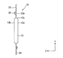
- the power supply terminal 22 has a positive terminal 22p and a negative terminal 22n.
- the positive electrode side terminal 22 p is electrically connected to the positive electrode side terminal of the smoothing capacitor 4.
- the positive electrode side terminal 22 p is electrically connected to the positive electrode side line 6.
- the positive electrode side terminal 22p is a main terminal through which a main current flows.
- the positive electrode side terminal 22p is also referred to as a high potential power supply terminal or a P terminal.
- the positive electrode side terminal 22p is connected to the first heat sink 14H and extends in the Y direction from the first heat sink 14H. In this embodiment, the positive electrode side terminal 22p is provided integrally with the first heat sink 14H by processing the same metal plate.
- the positive electrode side terminal 22p is continuous with one end of the first heat sink 14H in the Y direction.
- the positive electrode side terminal 22 p is extended in the Y direction and protrudes to the outside from the side surface 13 c of the sealing resin body 13.
- the negative terminal 22 n is electrically connected to the negative terminal of the smoothing capacitor 4.
- the negative electrode side terminal 22 n is electrically connected to the negative electrode side line 7.
- the negative electrode side terminal 22 n is a main terminal through which a main current flows.
- the negative terminal 22n is also referred to as a low potential power terminal or an N terminal.
- the negative electrode side terminal 22 n is arranged such that a portion thereof overlaps the third joint portion 20 c in projection view from the Z direction.
- the negative electrode side terminal 22 n is disposed on the IGBT 11 L side with respect to the third joint portion 20 c in the Z direction.
- the negative electrode side terminal 22 n and the third joint portion 20 c are also connected via solder.
- the negative electrode side terminal 22 n is extended in the Y direction and protrudes to the outside from the same side surface 13 c as the positive electrode side terminal 22 p.
- the output terminal 23 is electrically connected to the connection point of the upper and lower arms.
- the output terminal 23 is a main terminal through which a main current flows.
- the output terminal 23 is electrically connected to the coil of the corresponding phase of the motor 3.
- the output terminal 23 is also referred to as an AC terminal or an O terminal.
- the output terminal 23 is connected to the first heat sink 14L, and extends from the first heat sink 14L in the Y direction to the same side as the positive electrode side terminal 22p.
- the output terminal 23 is provided integrally with the first heat sink 14L by processing the same metal plate.
- the output terminal 23 is connected to one end in the Y direction of the first heat sink 14L.
- the output terminal 23 is extended in the Y direction, and protrudes outward from the same side surface 13c as the positive electrode terminal 22p and the negative electrode terminal 22n.
- the protruding portions of the positive electrode terminal 22p, the negative electrode terminal 22n, and the output terminal 23 from the sealing resin body 13 are arranged at substantially the same position in the Z direction.
- the positive terminal 22p, the negative terminal 22n, and the output terminal 23 are arranged in this order. That is, the projecting portion of the output terminal 23 is disposed at one end, and the projecting portion of the positive electrode side terminal 22p is disposed at the other end. And the protrusion part of the negative electrode side terminal 22n is arrange
- the negative electrode side terminal 22n is disposed adjacent to the positive electrode side terminal 22p.
- the positive electrode side terminal 22p, the negative electrode side terminal 22n, and the output terminal 23 each have a substantially flat plate shape, and the thicknesses in the Z direction are substantially equal to each other. Therefore, the thicknesses of the projecting portions of the positive electrode terminal 22p, the negative electrode terminal 22n, and the output terminal 23 are substantially equal to one another. Further, the widths of the projecting portions of the positive electrode terminal 22p, the negative electrode terminal 22n, and the output terminal 23 are substantially equal to one another.
- the width is a direction orthogonal to both the Y direction which is the direction of protrusion from the side surface 13 c and the Z direction which is the plate thickness direction, that is, the length in the X direction.
- the protrusion length of the positive electrode terminal 22p is shorter than the protrusion length of the negative electrode terminal 22n.
- the protruding length is a length extended to the outside with the side surface 13 c of the sealing resin body 13 as a position reference.
- the protrusion length of the output terminal 23 is longer than the protrusion length of the negative electrode side terminal 22 n. That is, as for the projection length, the positive electrode side terminal 22p is shortest and the output terminal 23 is longest.
- the projection length of the negative electrode side terminal 22n is an intermediate length.
- the positive terminal 22p may be a separate member from the first heat sink 14H and may be connected to the first heat sink 14H to be connected to the first heat sink 14H.
- the negative electrode side terminal 22n may be provided integrally with the third joint portion 20c, and thus with the second heat sink 18L.
- the output terminal 23 may be a separate member from the first heat sink 14L, and connected to the first heat sink 14L by being connected to the first heat sink 14L.
- the signal terminal 24 is electrically connected to the corresponding pad of the IGBTs 11H and 11L through the bonding wire 25.
- an aluminum-based bonding wire 25 is employed.
- the signal terminal 24 is extended in the Y direction, and protrudes outward from the surface of the sealing resin body 13 opposite to the side surface 13 c.
- the first heat sinks 14H and 14L, the first joint portion 20a, the positive terminal 22p, the negative terminal 22n, the output terminal 23, and the signal terminal 34 are formed of the same metal plate (lead frame). There is.
- the bus bar 26 electrically relays the IGBTs 11 H and 11 L constituting the upper and lower arms and the external device, specifically the smoothing capacitor 4.
- the bus bar 26 has a positive electrode side bus bar 26p and a negative electrode side bus bar 26n.
- the positive electrode side bus bar 26 p electrically relays the collector electrode 11 c of the IGBT 11 H and the positive electrode side terminal of the smoothing capacitor 4.
- the positive electrode side bus bar 26 p constitutes at least a part of the positive electrode side line 6.
- One end of the positive electrode side bus bar 26p is continuous with the vicinity of the tip of the protruding portion of the positive electrode side terminal 22p.
- the negative bus bar 26 n electrically relays the emitter electrode 11 e of the IGBT 11 L and the negative terminal of the smoothing capacitor 4.
- the negative bus bar 26 n constitutes at least a part of the negative line 7.
- One end of the negative electrode side bus bar 26 n is continuous with the vicinity of the tip of the projecting portion of the negative electrode side terminal 22 n.
- the positive bus bar 26 p and the negative bus bar 26 n extend in the X direction, with the thickness direction being the Y direction, at least in part from the connection portion with the corresponding power supply terminal 22.
- Positive electrode side bus bar 26 p and negative electrode side bus bar 26 n are arranged to face each other with a predetermined gap (interval) in the Y direction.
- positive electrode side bus bar 26p and negative electrode side bus bar 26n are arranged in a parallel plate configuration.
- An end face connected to the surface in the plate thickness direction of positive electrode side bus bar 26p is connected to the surface in the plate thickness direction of positive electrode side terminal 22p.
- an end face connected to the surface in the thickness direction of the negative bus bar 26n is connected to the surface in the thickness direction of the negative terminal 22n.
- the bus bar 26 corresponding to the power supply terminal 22 is connected by laser welding.
- An insulator such as an insulating paper or an insulating plate may be disposed between the positive electrode side bus bar 26p and the negative electrode side bus bar 26n to have a stacked structure of the positive electrode side bus bar 26p, the insulator, and the negative electrode side bus bar 26n. Thereby, parasitic inductance can be reduced.
- the IGBTs 11H and 11L, a part of each of the first heat sinks 14H and 14L, the terminal 16, a part of each of the second heat sinks 18H and 18L, and the power supply terminal A portion of each of the portions 22, a portion of the output terminal, and a portion of the signal terminal 35 are integrally sealed.
- the sealing resin body 13 seals two IGBTs 11H and 11L that constitute upper and lower arms for one phase. For this reason, the semiconductor module 10 is also referred to as a 2 in 1 package.
- the heat release surfaces 14a of the first heat sinks 14H and 14L are located in the same plane, and are substantially flush with the one surface 13a of the sealing resin body 13.
- the heat radiation surfaces 18a of the second heat sinks 18H and 18L are located in the same plane, and are substantially flush with the back surface 13b of the sealing resin body 13.
- the semiconductor module 10 has a double-sided heat radiation structure in which the heat radiation surfaces 14 a and 18 a are both exposed from the sealing resin body 13.
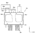
- the comparative example of FIG. 5 shows a semiconductor module of a conventional configuration.
- r is added to the end of the reference numerals of the present embodiment for the elements which are the same as or related to the elements of the present embodiment.
- the protrusion length of the positive electrode side terminal 22 pr is longer than the protrusion length of the negative electrode side terminal 22 nr. For this reason, in order to extend the negative electrode side bus bar 26nr connected to the negative electrode side terminal 22nr disposed in the middle in the X direction, the positive electrode side terminal 22pr disposed at the end must be disposed so as to avoid. As described above, the positive electrode side terminal 22pr must be bypassed, and the length of the negative electrode side bus bar 26nr becomes long, so that the parasitic inductance and hence the surge voltage increase.
- the protrusion length of the positive electrode terminal 22p is shorter than the protrusion length of the negative electrode terminal 22n.
- the negative bus bar 26n can be extended in the X direction without being disposed so as to avoid the positive terminal 22p disposed at the end.
- parasitic inductance can be reduced.
- the suppression of the detour makes it possible to face each other between the positive bus bar 26p connected to the positive terminal 22p and the negative bus bar 26n connected to the negative terminal 22n.
- Opposing arrangement also contributes to the reduction of parasitic inductance.
- the surge voltage can be reduced.
- the width and thickness of each of the projecting portions of the positive terminal 22p, the negative terminal 22n, and the output terminal 23, which are main terminals, are equal. Since the thicknesses are substantially equal to each other, it is possible to suppress the formation of a gap with the mold when the sealing resin body 13 is formed. Also, the configuration of the mold can be simplified. Furthermore, the bias of the pressure received by being pinched by the mold can also be suppressed. Further, since the widths are substantially equal to each other, the body size in the X direction, which is the alignment direction, can be miniaturized while securing the rated current density.
- the example in which the semiconductor module 10 includes the bus bar 26 is shown.
- the bus bar 26 may not be provided. Even in the configuration in which the bus bar 26 is not provided, the protrusion length of the positive electrode terminal 22p is shorter than the protrusion length of the negative electrode terminal 22n. Therefore, in the configuration in which the bus bar 26 is connected to the power supply terminal 22 in the X direction, the parasitic inductance can be reduced by suppressing the detour, and hence the surge voltage can be reduced.
- the protruding portion of the negative electrode side terminal 22 n is disposed in the middle, and the protruding portion of the positive electrode side terminal 22 p is disposed at the end opposite to the output terminal 23.
- the projection length of the negative electrode terminal 22n may be shorter than the projection length of the positive electrode terminal 22p.
- Second Embodiment This embodiment can refer to the preceding embodiments. Therefore, the description of the parts common to the semiconductor module 10 and the power conversion device 1 shown in the preceding embodiment will be omitted.
- the widths of the protruding portions of the positive electrode terminal 22 p and the negative electrode terminal 22 n are wider than the width of the protruding portion of the output terminal 23.
- the thickness of the protruding portion of the power supply terminal 22 and the thickness of the protruding portion of the output terminal 23 are substantially equal to each other.
- the cross-sectional areas of the projecting portions of the positive electrode side terminal 22p and the negative electrode side terminal 22n, which are the power supply terminals 22, are larger than the cross-sectional area of the projecting portion of the output terminal 23.
- the cross-sectional area is an area orthogonal to the Y direction which is the protruding direction.
- the width of the protruding portion of each of the positive electrode side terminal 22p and the negative electrode side terminal 22n, which are the power supply terminals 22, is widened to increase the cross-sectional area.
- the parasitic inductance of the power supply terminal 22 can be reduced, and hence the surge voltage can be reduced.
- the parasitic inductance of the output terminal 23 is not related to the surge voltage.
- the protruding portions of each of the positive electrode side terminal 22 p and the negative electrode side terminal 22 n may be thicker than the protruding portion of the output terminal 23 to thereby increase the cross-sectional area.
- the width of the protruding portion of the power supply terminal 22 and the width of the protruding portion of the output terminal 23 are substantially equal to each other.
- the cross-sectional area may be made different by adjusting both the width and the plate thickness.
- the bus bar 26 may not be provided.
- the positive terminal 22p may be disposed in the middle, and the negative terminal 22n may be disposed at the end.
- This embodiment can refer to the preceding embodiments. Therefore, the description of the parts common to the semiconductor module 10 and the power conversion device 1 shown in the preceding embodiment will be omitted.
- the width of the protruding portion of the negative electrode terminal 22n disposed in the middle among the positive electrode terminal 22p and the negative electrode terminal 22n, which are the power supply terminals 22, is disposed at the end.
- the width is larger than the width of the protruding portion of the positive electrode side terminal 22p.
- the thickness of the protruding portion of the negative electrode terminal 22n and the thickness of the protruding portion of the positive electrode terminal 22p are substantially equal to each other.
- the cross-sectional area of the protruding portion of the negative electrode terminal 22n is larger than the cross-sectional area of the protruding portion of the positive electrode terminal 22p.
- the projecting portion of the negative electrode side terminal 22n disposed in the middle of the two adjacent power supply terminals 22 is made wide to increase the cross sectional area.
- the balance of the parasitic inductance in which the power supply terminal 22 and the bus bar 26 are combined can be made closer, preferably substantially equal, on the positive electrode side and the negative electrode side. Therefore, the surge stresses of the IGBTs 11H and 11L constituting the upper and lower arms can be made to be close to each other, preferably substantially equal.
- specifications of the drive circuit and the heat dissipation structure can be matched by the IGBTs 11H and 11L.
- the protruding portion of the negative electrode side terminal 22n may be thicker than the protruding portion of the positive electrode side terminal 22p, thereby increasing the cross-sectional area.
- the bus bar 26 may not be provided.
- the positive terminal 22p may be disposed at the center and the negative terminal 22n may be disposed at the end.
- the semiconductor module 10 includes the positive electrode side bus bar 26p and the negative electrode side bus bar 26n.
- the negative bus bar 26n connected to the negative terminal 22n disposed in the middle is thicker than the positive bus bar 26p connected to the positive terminal 22p disposed at the end.
- the width of the negative side bus bar 26 n and the width of the positive side bus bar 26 p are substantially equal to each other.
- the cross-sectional area of the negative bus bar 26n is larger than the cross-sectional area of the positive bus bar 26p.
- the cross-sectional area is an area orthogonal to the extending direction.
- the width is a direction perpendicular to both the extending direction and the thickness direction, that is, the length in the Z direction.
- the negative bus bar 26n connected to the middle negative terminal 22n is thickened to increase the cross-sectional area.
- the balance of the parasitic inductance of the combination of the power supply terminal 22 and the bus bar 26 can be made closer, preferably substantially equal, on the positive electrode side and the negative electrode side. Therefore, the surge stresses of the IGBTs 11H and 11L constituting the upper and lower arms can be made to be close to each other, preferably substantially equal.
- the width of the negative bus bar 26n may be increased to increase the cross-sectional area. Further, in the configuration in which the positive electrode side terminal 22p is disposed at the center and the negative electrode side terminal 22n is disposed at the end, the cross sectional area of the positive electrode side bus bar 26p may be larger than that of the negative electrode side bus bar 26n.
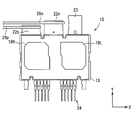
- a notch 27 is formed in the protruding portion of the positive electrode side terminal 22p which is the power supply terminal 22 disposed at the end opposite to the output terminal 23.
- the notch 27 penetrates the positive electrode side terminal 22p in the plate thickness direction.
- the notches 27 are respectively formed at both ends in the Y direction which is the width direction.
- the portion where the notch 27 is formed is a narrow portion with respect to the portion where the notch 27 is not formed.
- the notch 27 corresponds to a first notch.
- the spring property of the positive electrode side terminal 22p is enhanced. Even while shortening the length of the positive electrode side terminal 22p in order to suppress detouring, stress such as vibration during traveling of the vehicle can be alleviated by the spring deformation of the positive electrode side terminal 22p. Therefore, the connection reliability of positive electrode side terminal 22p and positive electrode side bus bar 26p can be improved.
- the bent portion When the bent portion is provided to enhance the spring property, the protrusion length of the positive electrode side terminal 22p becomes long, and the parasitic inductance is increased.
- the spring property is enhanced by the notches 27, connection reliability can be improved while suppressing an increase in parasitic inductance as compared with the case where the bent portion is provided.
- the notch 28 is also formed in the protruding portion of the negative electrode side terminal 22 n which is the power supply terminal 22 disposed in the middle.
- the notch 28 penetrates the negative electrode side terminal 22 n in the plate thickness direction.
- the notches 28 are respectively formed at both ends in the Y direction which is the width direction.
- the portion where the notch 28 is formed is a narrow portion with respect to the portion where the notch 28 is not formed.
- the notch 28 corresponds to a second notch.
- the spring property of the negative electrode side terminal 22n is enhanced.
- the spring property is enhanced by the bent portion
- the projection length of the negative electrode side terminal 22n becomes long, and the parasitic inductance increases.
- connection reliability can be improved while suppressing an increase in parasitic inductance as compared with the case where the bent portion is provided.
- the notch 29 is also formed in the output terminal 23 having the longest projection length.
- the notch 29 penetrates the output terminal 23 in the plate thickness direction.
- the notches 29 are respectively formed at both ends in the Y direction which is the width direction.
- the portion where the notch 29 is formed is a narrow portion with respect to the portion where the notch 29 is not formed.
- a bent portion 30 is formed in the narrow portion of the output terminal 23.
- the bent portion 30 has a substantially semicircular shape as shown in FIG.
- the springiness of the output terminal 23 is enhanced by providing the bent portion 30, and stress such as vibration can be relieved. Therefore, the connection reliability of the connection portion between the not-shown bus bar and the output terminal 23 constituting the output line 8 can be improved.
- the bending portion 30 By providing the bent portion 30, even if the projecting length of the output terminal 23 is increased, the surge voltage is not affected.
- the provision of the bending portion 30 can improve the springability more than the notch.
- the bent portion 30 since the bent portion 30 is provided in the narrow portion by the notch 29, the spring property can be further enhanced.
- the configuration may be such that only the bending portion 30 is provided without the notch 29.
- notches 27 to 29 and the bent portion 30 are shown, but the present invention is not limited to this. It is preferable to have at least the notch 27. Preferably, notches 27 and 28 may be provided. More preferably, the notches 27 and 28 and the bending portion 30 may be provided.
- IGBT11H and FWD12H were formed in the same chip and IGBT11L and FWD12L were formed in the same chip, although it showed an example, it is not limited to this. It may be a separate chip.
- the semiconductor module 10 has the terminal 16
- the terminal 16 may not be provided.
- heat sinking surfaces 14a and 18a are exposed from the corresponding sealing resin body 13
- the heat dissipating surfaces 14a and 18a may not be exposed.
- the semiconductor element which constitutes the upper and lower arms is not limited to the IGBT.
- a MOSFET can be employed.
- the upper arm is comprised by one IGBT11H and the example which a lower arm is comprised by one IGBT11L was shown, it is not limited to this.
- a plurality of semiconductor elements may be connected in parallel to constitute each arm.
Landscapes
- Engineering & Computer Science (AREA)
- Power Engineering (AREA)
- Microelectronics & Electronic Packaging (AREA)
- General Physics & Mathematics (AREA)
- Physics & Mathematics (AREA)
- Computer Hardware Design (AREA)
- Condensed Matter Physics & Semiconductors (AREA)
- Multimedia (AREA)
- Signal Processing (AREA)
- Inverter Devices (AREA)
- Closed-Circuit Television Systems (AREA)
- Computer Vision & Pattern Recognition (AREA)
- Theoretical Computer Science (AREA)
- Quality & Reliability (AREA)
- Lead Frames For Integrated Circuits (AREA)
Priority Applications (2)
| Application Number | Priority Date | Filing Date | Title |
|---|---|---|---|
| CN201880062126.8A CN111133573A (zh) | 2017-09-28 | 2018-08-01 | 半导体模块 |
| US16/814,260 US20200211954A1 (en) | 2017-09-28 | 2020-03-10 | Semiconductor module |
Applications Claiming Priority (2)
| Application Number | Priority Date | Filing Date | Title |
|---|---|---|---|
| JP2017-188647 | 2017-09-28 | ||
| JP2017188647A JP2019067813A (ja) | 2017-09-28 | 2017-09-28 | 半導体モジュール |
Related Child Applications (1)
| Application Number | Title | Priority Date | Filing Date |
|---|---|---|---|
| US16/814,260 Continuation US20200211954A1 (en) | 2017-09-28 | 2020-03-10 | Semiconductor module |
Publications (1)
| Publication Number | Publication Date |
|---|---|
| WO2019064904A1 true WO2019064904A1 (ja) | 2019-04-04 |
Family
ID=65901209
Family Applications (1)
| Application Number | Title | Priority Date | Filing Date |
|---|---|---|---|
| PCT/JP2018/028790 Ceased WO2019064904A1 (ja) | 2017-09-28 | 2018-08-01 | 半導体モジュール |
Country Status (4)
| Country | Link |
|---|---|
| US (2) | US11431255B2 (enExample) |
| JP (1) | JP2019067813A (enExample) |
| CN (1) | CN111133573A (enExample) |
| WO (1) | WO2019064904A1 (enExample) |
Cited By (1)
| Publication number | Priority date | Publication date | Assignee | Title |
|---|---|---|---|---|
| US11587921B2 (en) * | 2019-09-30 | 2023-02-21 | Denso Corporation | Semiconductor device |
Families Citing this family (2)
| Publication number | Priority date | Publication date | Assignee | Title |
|---|---|---|---|---|
| US20240430560A1 (en) * | 2021-03-30 | 2024-12-26 | Nec Corporation | Authentication device, processing method, and program |
| JP2023088055A (ja) * | 2021-12-14 | 2023-06-26 | 富士電機株式会社 | 半導体装置 |
Citations (5)
| Publication number | Priority date | Publication date | Assignee | Title |
|---|---|---|---|---|
| JP2003218311A (ja) * | 2002-01-21 | 2003-07-31 | Aisin Seiki Co Ltd | リード端子付電子部品 |
| JP2006295997A (ja) * | 2005-04-05 | 2006-10-26 | Denso Corp | 電力変換装置 |
| WO2014136271A1 (ja) * | 2013-03-08 | 2014-09-12 | 株式会社東芝 | 車両用電力変換装置 |
| JP2016025298A (ja) * | 2014-07-24 | 2016-02-08 | セイコーエプソン株式会社 | 電子部品、電子部品の製造方法、電子機器、および移動体 |
| JP2017099140A (ja) * | 2015-11-24 | 2017-06-01 | トヨタ自動車株式会社 | 電力変換装置 |
Family Cites Families (33)
| Publication number | Priority date | Publication date | Assignee | Title |
|---|---|---|---|---|
| US6292098B1 (en) * | 1998-08-31 | 2001-09-18 | Hitachi, Ltd. | Surveillance system and network system |
| JP2000358240A (ja) | 1999-06-16 | 2000-12-26 | Nippon Telegr & Teleph Corp <Ntt> | 監視カメラ制御装置 |
| US7394916B2 (en) * | 2003-02-10 | 2008-07-01 | Activeye, Inc. | Linking tracked objects that undergo temporary occlusion |
| US7242423B2 (en) * | 2003-06-16 | 2007-07-10 | Active Eye, Inc. | Linking zones for object tracking and camera handoff |
| US7450638B2 (en) * | 2003-07-21 | 2008-11-11 | Sony Corporation | Power-line communication based surveillance system |
| JP4893649B2 (ja) * | 2008-02-08 | 2012-03-07 | 富士通株式会社 | 帯域制御サーバ及び帯域制御プログラム並びに監視システム |
| KR100994722B1 (ko) * | 2008-08-01 | 2010-11-16 | 포항공과대학교 산학협력단 | 카메라 핸드오프를 이용한 다중 카메라상의 연속적인 물체추적 방법 |
| US20100245588A1 (en) * | 2009-03-31 | 2010-09-30 | Acuity Systems Inc. | Tag tracking system |
| WO2010144566A1 (en) * | 2009-06-09 | 2010-12-16 | Wayne State University | Automated video surveillance systems |
| JP5402431B2 (ja) * | 2009-09-11 | 2014-01-29 | 沖電気工業株式会社 | カメラ制御装置 |
| IL201129A (en) * | 2009-09-23 | 2014-02-27 | Verint Systems Ltd | A system and method for automatically switching cameras according to location measurements |
| JP5213883B2 (ja) | 2010-01-19 | 2013-06-19 | 三菱電機株式会社 | 合成表示装置 |
| WO2011114799A1 (ja) * | 2010-03-15 | 2011-09-22 | オムロン株式会社 | 監視カメラ端末 |
| JP5556599B2 (ja) * | 2010-11-04 | 2014-07-23 | 株式会社デンソー | 電力変換装置 |
| KR101248054B1 (ko) * | 2011-05-04 | 2013-03-26 | 삼성테크윈 주식회사 | 물체의 이동 경로를 추적하는 물체 추적 시스템 및 그 방법 |
| KR101970197B1 (ko) * | 2012-10-29 | 2019-04-18 | 에스케이 텔레콤주식회사 | 복수의 카메라 제어 방법과 그를 위한 카메라 제어 장치 |
| JP2015002553A (ja) * | 2013-06-18 | 2015-01-05 | キヤノン株式会社 | 情報処理システムおよびその制御方法 |
| WO2015019546A1 (ja) * | 2013-08-09 | 2015-02-12 | パナソニックIpマネジメント株式会社 | 無線カメラシステム、センタ装置、画像表示方法、画像表示プログラム |
| JP6221542B2 (ja) * | 2013-09-16 | 2017-11-01 | 株式会社デンソー | 半導体装置 |
| GB2542982A (en) * | 2014-07-15 | 2017-04-05 | Motorola Solutions Inc | Method and apparatus for notifying a user whether or not they are within a camera's field of view |
| KR102150703B1 (ko) * | 2014-08-14 | 2020-09-01 | 한화테크윈 주식회사 | 지능형 비디오 분석 시스템에서 비디오를 분석하는 방법 및 시스템 |
| US20160094810A1 (en) * | 2014-09-30 | 2016-03-31 | Verizon Patent And Licensing Inc. | System and method for providing neighborhood services through networked cameras |
| US20160127695A1 (en) * | 2014-10-30 | 2016-05-05 | Motorola Solutions, Inc | Method and apparatus for controlling a camera's field of view |
| KR102174839B1 (ko) * | 2014-12-26 | 2020-11-05 | 삼성전자주식회사 | 보안 시스템 및 그 운영 방법 및 장치 |
| JP6555906B2 (ja) | 2015-03-05 | 2019-08-07 | キヤノン株式会社 | 情報処理装置、情報処理方法、およびプログラム |
| JP6595287B2 (ja) | 2015-03-27 | 2019-10-23 | エヌ・ティ・ティ・コミュニケーションズ株式会社 | 監視システム、監視方法、解析装置及び解析プログラム |
| US11019268B2 (en) * | 2015-03-27 | 2021-05-25 | Nec Corporation | Video surveillance system and video surveillance method |
| US11272089B2 (en) * | 2015-06-16 | 2022-03-08 | Johnson Controls Tyco IP Holdings LLP | System and method for position tracking and image information access |
| AU2015234329A1 (en) * | 2015-09-30 | 2017-04-13 | Canon Kabushiki Kaisha | Method, system and apparatus for processing an image |
| JP6758858B2 (ja) * | 2016-02-29 | 2020-09-23 | キヤノン株式会社 | 通信装置、通信方法及びプログラム |
| CN106412414B (zh) * | 2016-06-08 | 2019-12-27 | 同济大学 | 追踪系统、摄像头、监测方法、及监测系统 |
| JP2018093401A (ja) * | 2016-12-05 | 2018-06-14 | キヤノンイメージングシステムズ株式会社 | 映像監視装置、映像監視方法および映像監視システム |
| JP7003628B2 (ja) * | 2017-12-19 | 2022-01-20 | 富士通株式会社 | 物体追跡プログラム、物体追跡装置、及び物体追跡方法 |
-
2017
- 2017-09-28 JP JP2017188647A patent/JP2019067813A/ja active Pending
-
2018
- 2018-08-01 WO PCT/JP2018/028790 patent/WO2019064904A1/ja not_active Ceased
- 2018-08-01 CN CN201880062126.8A patent/CN111133573A/zh not_active Withdrawn
- 2018-08-02 US US16/634,658 patent/US11431255B2/en active Active
-
2020
- 2020-03-10 US US16/814,260 patent/US20200211954A1/en not_active Abandoned
Patent Citations (5)
| Publication number | Priority date | Publication date | Assignee | Title |
|---|---|---|---|---|
| JP2003218311A (ja) * | 2002-01-21 | 2003-07-31 | Aisin Seiki Co Ltd | リード端子付電子部品 |
| JP2006295997A (ja) * | 2005-04-05 | 2006-10-26 | Denso Corp | 電力変換装置 |
| WO2014136271A1 (ja) * | 2013-03-08 | 2014-09-12 | 株式会社東芝 | 車両用電力変換装置 |
| JP2016025298A (ja) * | 2014-07-24 | 2016-02-08 | セイコーエプソン株式会社 | 電子部品、電子部品の製造方法、電子機器、および移動体 |
| JP2017099140A (ja) * | 2015-11-24 | 2017-06-01 | トヨタ自動車株式会社 | 電力変換装置 |
Cited By (1)
| Publication number | Priority date | Publication date | Assignee | Title |
|---|---|---|---|---|
| US11587921B2 (en) * | 2019-09-30 | 2023-02-21 | Denso Corporation | Semiconductor device |
Also Published As
| Publication number | Publication date |
|---|---|
| JP2019067813A (ja) | 2019-04-25 |
| US20200211954A1 (en) | 2020-07-02 |
| CN111133573A (zh) | 2020-05-08 |
| US11431255B2 (en) | 2022-08-30 |
| US20200204724A1 (en) | 2020-06-25 |
Similar Documents
| Publication | Publication Date | Title |
|---|---|---|
| US11545419B2 (en) | Semiconductor package having an additional material with a comparative tracking index (CTI) higher than that of encapsulant resin material formed between two terminals | |
| CN110998838B (zh) | 半导体模块 | |
| JP6394489B2 (ja) | 半導体装置 | |
| US8461623B2 (en) | Power semiconductor module | |
| US11380656B2 (en) | Semiconductor device | |
| CN109417066B (zh) | 半导体装置 | |
| US11456238B2 (en) | Semiconductor device including a semiconductor chip connected with a plurality of main terminals | |
| CN111480231B (zh) | 电力转换装置 | |
| CN110178304B (zh) | 半导体装置 | |
| CN109952639A (zh) | 半导体装置、逆变器单元及汽车 | |
| US10978381B2 (en) | Semiconductor device | |
| US20200211954A1 (en) | Semiconductor module | |
| JP6123722B2 (ja) | 半導体装置 | |
| CN112582356A (zh) | 半导体器件 | |
| CN114144965B (zh) | 电路装置 | |
| US12500185B2 (en) | Semiconductor device | |
| US20230230940A1 (en) | Semiconductor device | |
| JP2024018064A (ja) | 半導体装置 | |
| CN116264219A (zh) | 半导体装置 |
Legal Events
| Date | Code | Title | Description |
|---|---|---|---|
| 121 | Ep: the epo has been informed by wipo that ep was designated in this application |
Ref document number: 18861485 Country of ref document: EP Kind code of ref document: A1 |
|
| NENP | Non-entry into the national phase |
Ref country code: DE |
|
| 122 | Ep: pct application non-entry in european phase |
Ref document number: 18861485 Country of ref document: EP Kind code of ref document: A1 |