WO2019031172A1 - 電力変換装置 - Google Patents
電力変換装置 Download PDFInfo
- Publication number
- WO2019031172A1 WO2019031172A1 PCT/JP2018/026932 JP2018026932W WO2019031172A1 WO 2019031172 A1 WO2019031172 A1 WO 2019031172A1 JP 2018026932 W JP2018026932 W JP 2018026932W WO 2019031172 A1 WO2019031172 A1 WO 2019031172A1
- Authority
- WO
- WIPO (PCT)
- Prior art keywords
- flow path
- housing
- electrical component
- path forming
- power conversion
- Prior art date
Links
Images


Classifications
-
- H—ELECTRICITY
- H05—ELECTRIC TECHNIQUES NOT OTHERWISE PROVIDED FOR
- H05K—PRINTED CIRCUITS; CASINGS OR CONSTRUCTIONAL DETAILS OF ELECTRIC APPARATUS; MANUFACTURE OF ASSEMBLAGES OF ELECTRICAL COMPONENTS
- H05K7/00—Constructional details common to different types of electric apparatus
- H05K7/20—Modifications to facilitate cooling, ventilating, or heating
- H05K7/2089—Modifications to facilitate cooling, ventilating, or heating for power electronics, e.g. for inverters for controlling motor
- H05K7/209—Heat transfer by conduction from internal heat source to heat radiating structure
-
- H—ELECTRICITY
- H01—ELECTRIC ELEMENTS
- H01G—CAPACITORS; CAPACITORS, RECTIFIERS, DETECTORS, SWITCHING DEVICES OR LIGHT-SENSITIVE DEVICES, OF THE ELECTROLYTIC TYPE
- H01G2/00—Details of capacitors not covered by a single one of groups H01G4/00-H01G11/00
- H01G2/02—Mountings
-
- H—ELECTRICITY
- H01—ELECTRIC ELEMENTS
- H01G—CAPACITORS; CAPACITORS, RECTIFIERS, DETECTORS, SWITCHING DEVICES OR LIGHT-SENSITIVE DEVICES, OF THE ELECTROLYTIC TYPE
- H01G2/00—Details of capacitors not covered by a single one of groups H01G4/00-H01G11/00
- H01G2/02—Mountings
- H01G2/04—Mountings specially adapted for mounting on a chassis
-
- H—ELECTRICITY
- H01—ELECTRIC ELEMENTS
- H01G—CAPACITORS; CAPACITORS, RECTIFIERS, DETECTORS, SWITCHING DEVICES OR LIGHT-SENSITIVE DEVICES, OF THE ELECTROLYTIC TYPE
- H01G2/00—Details of capacitors not covered by a single one of groups H01G4/00-H01G11/00
- H01G2/08—Cooling arrangements; Heating arrangements; Ventilating arrangements
-
- H—ELECTRICITY
- H01—ELECTRIC ELEMENTS
- H01G—CAPACITORS; CAPACITORS, RECTIFIERS, DETECTORS, SWITCHING DEVICES OR LIGHT-SENSITIVE DEVICES, OF THE ELECTROLYTIC TYPE
- H01G4/00—Fixed capacitors; Processes of their manufacture
- H01G4/32—Wound capacitors
-
- H—ELECTRICITY
- H02—GENERATION; CONVERSION OR DISTRIBUTION OF ELECTRIC POWER
- H02K—DYNAMO-ELECTRIC MACHINES
- H02K5/00—Casings; Enclosures; Supports
- H02K5/04—Casings or enclosures characterised by the shape, form or construction thereof
- H02K5/20—Casings or enclosures characterised by the shape, form or construction thereof with channels or ducts for flow of cooling medium
- H02K5/203—Casings or enclosures characterised by the shape, form or construction thereof with channels or ducts for flow of cooling medium specially adapted for liquids, e.g. cooling jackets
-
- H—ELECTRICITY
- H02—GENERATION; CONVERSION OR DISTRIBUTION OF ELECTRIC POWER
- H02M—APPARATUS FOR CONVERSION BETWEEN AC AND AC, BETWEEN AC AND DC, OR BETWEEN DC AND DC, AND FOR USE WITH MAINS OR SIMILAR POWER SUPPLY SYSTEMS; CONVERSION OF DC OR AC INPUT POWER INTO SURGE OUTPUT POWER; CONTROL OR REGULATION THEREOF
- H02M7/00—Conversion of ac power input into dc power output; Conversion of dc power input into ac power output
- H02M7/42—Conversion of dc power input into ac power output without possibility of reversal
- H02M7/44—Conversion of dc power input into ac power output without possibility of reversal by static converters
- H02M7/48—Conversion of dc power input into ac power output without possibility of reversal by static converters using discharge tubes with control electrode or semiconductor devices with control electrode
-
- H—ELECTRICITY
- H05—ELECTRIC TECHNIQUES NOT OTHERWISE PROVIDED FOR
- H05K—PRINTED CIRCUITS; CASINGS OR CONSTRUCTIONAL DETAILS OF ELECTRIC APPARATUS; MANUFACTURE OF ASSEMBLAGES OF ELECTRICAL COMPONENTS
- H05K7/00—Constructional details common to different types of electric apparatus
- H05K7/20—Modifications to facilitate cooling, ventilating, or heating
- H05K7/2089—Modifications to facilitate cooling, ventilating, or heating for power electronics, e.g. for inverters for controlling motor
- H05K7/20927—Liquid coolant without phase change
Definitions
- the present disclosure relates to a power converter.
- an electric component such as a capacitor constituting a power conversion circuit and a case for housing the same are provided, and the case has a refrigerant flow path through which a refrigerant for cooling the electric component flows.
- Some are integrally formed with the housing.
- the capacitor constituting the power conversion circuit is pressed against the outer wall surface of the refrigerant flow path integrally formed in the housing so that both are closely attached to the housing. It is fixed. Thereby, the cooling of the capacitor is promoted to enhance the heat dissipation.
- the present disclosure is intended to provide a power converter that can obtain a high cooling effect while absorbing dimensional variations of electrical components.
- One aspect of the present disclosure is an electrical component that constitutes at least a part of a power conversion circuit, A housing that accommodates the electrical component and the electrical component is fixed; A flow path forming portion that forms a refrigerant flow path through which the refrigerant flows, and is thermally connected to the electrical component, Equipped with The flow passage forming unit is a separate member from the casing, and an elastically deformable spacer is provided between the flow passage forming unit and the casing.
- the flow passage forming portion to which the electric component is thermally connected is formed separately from the housing. And, an elastically deformable spacer is provided between the housing and the flow path forming portion. Therefore, the relative position between the housing and the flow path forming portion can be easily changed by elastically deforming the spacer. Then, by adjusting the relative position of the casing and the flow path forming portion in accordance with the dimensional variation of the electrical component, the dimensional variation of the electrical component can be absorbed. Therefore, the cooling effect of the electrical component can be improved while suppressing the generation of stress in the electrical component.
- FIG. 1 is a cross-sectional conceptual view of a power conversion device according to a first embodiment
- FIG. 2 is a cross-sectional conceptual view of the power conversion device in the second embodiment
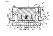
- FIG. 3 is a cross-sectional conceptual view of the power conversion device in the third embodiment.
- the power converter device 1 of this embodiment is equipped with the electrical component 10, the housing
- the electrical component 10 constitutes at least a part of a power conversion circuit.
- the housing 20 accommodates the electrical component 10 and the electrical component 10 is fixed.
- the flow path forming unit 30 forms a refrigerant flow path 31 through which the refrigerant flows, and is thermally connected to the electric component 10.
- the flow path forming unit 30 is a separate member from the housing 20, and an elastically deformable spacer 40 is provided between the flow path forming unit 30 and the housing 20.
- the power conversion device 1 of the present embodiment has a power conversion function such as an inverter or a converter.
- the power converter 1 can be mounted on an electric vehicle or the like.
- the side on which the flow path forming unit 30 is provided in the housing 20 is referred to as the lower side X1
- the opposite side is referred to as the upper side X2
- the vertical direction X is referred to as the vertical direction X.
- the electric component 10 shown in FIG. 1 constitutes a part of a power conversion circuit (not shown).
- the electrical component 10 can be, for example, a capacitor, a current sensor, a reactor, a power module, or the like, and is a capacitor in the present embodiment.
- the electrical component 10 includes a capacitor element 11 and a case 12.
- the capacitor element 11 comprises an electrode 13.
- the electrode 13 is a metallikon electrode formed by spraying metal melted by metallikon.
- the bus bar 50 is connected to the electrode 13 by the bonding member 14 made of solder.
- the bus bar 50 is connected to an electric component such as a power module having a semiconductor element (not shown).
- the case 12 of the electrical component 10 can be made of resin, but not limited to, and in this embodiment, made of PPS (polyphenyl sulfide) resin.
- the case 12 includes the capacitor element 11 and has a case fixing rib 15 for fixing to the case 20. Further, in the present embodiment, a part of the bus bar 50 is also located in the case 12.
- the lower surface 16 of the case 12 is flat.
- the housing 20 has four side walls 21 and has a substantially cylindrical shape with a lower side X1 and an upper side X2 opened.
- an electrical component 10 is housed inside the housing 20.
- a projecting portion 22 is provided on the inner side surface of the side wall 21 of the casing 20, and a casing fixing rib 15 of the electric component 10 is fixed to the projecting portion 22 by a fastening member 17.
- the electrical component 10 is attached to the housing 20.
- An upper lid member (not shown) is provided at the upper end portion of the housing 20, and the upper lid member covers the opening of the upper side X2 of the housing 20.
- the flow path forming unit 30 is formed separately from the housing 20.
- a refrigerant flow path 31 is provided inside the flow path formation unit 30.
- the refrigerant channel 31 has a refrigerant inlet for supplying the refrigerant to the refrigerant channel 31 and a refrigerant outlet for discharging the refrigerant from the refrigerant channel 31.
- a flow path forming portion fixing rib 32 projecting outward is provided. The flow path formation portion fixing rib 32 is fixed to the flange 23 of the housing 20 via the fastening member 44.
- the flow path forming unit 30 is attached to the lower end portion of the housing 20 and covers the opening of the lower side X1 of the housing 20.
- the flow path forming unit 30 also functions as a lid of the lower side X1 in the housing 20.
- a spacer 40 is interposed between the flow path forming portion 30 and the housing 20.
- the spacer 40 is made of an elastically deformable material.
- the spacer 40 is made of a material that can seal between the flow passage forming portion 30 and the housing 20.
- the spacer 40 is provided along the entire circumference of the lower end portion of the housing 20 to seal the space between the housing 20 and the flow path forming portion 30 so that water or the like infiltrates into the housing 20 from the outside. It is being prevented.
- the heat dissipation material 60 is provided between the lower surface 16 of the electric component 10 and the upper surface 33 of the flow path forming portion 30.
- the electrical component 10 and the flow path forming unit 30 are thermally connected to each other through the heat dissipation material 60.
- the lower surface 16 of the electric component 10 and the upper surface 33 of the flow path forming portion 30 are each planar and parallel to each other.
- the heat dissipation material 60 is in the form of a sheet.
- the shape of the heat dissipation material 60 is not particularly limited, but in the present embodiment, the shape is substantially the same as the lower surface 16 of the electric component 10 in a plan view.
- the thickness of the heat dissipation material 60 is not particularly limited, but is preferably 1.0 mm or less, and is about 0.1 mm in the present embodiment.
- the material of the heat dissipating material 60 can have a thermal conductivity higher than that of the material forming the flow path forming portion 30.
- the heat dissipating material 60 is preferably made of an elastically deformable material.
- the flow path forming unit 30 to which the electrical component 10 is thermally connected is formed separately from the housing 20.
- An elastically deformable spacer 40 intervenes between the housing 20 and the flow path forming unit 30. Therefore, by elastically deforming the spacer 40, the relative position between the housing 20 and the flow path forming portion 30 can be easily changed. Then, by adjusting the relative position between the housing 20 and the flow path forming unit 30 in accordance with the dimensional variation of the electrical component 10, the dimensional variation of the electrical component 10 can be absorbed. Therefore, the cooling effect of the electrical component 10 can be improved while suppressing the generation of stress in the electrical component 10.
- the heat dissipation material 60 is interposed between the electrical component 10 and the flow path forming portion 30. Thereby, the cooling effect of the electrical component 10 can be further improved. Furthermore, in the present embodiment, the heat dissipation material 60 is elastically deformable. As a result, it is possible to absorb the dimensional variation of the electrical component 10 by both the spacer 40 and the heat dissipation material 60, so that the dimensional variation of the electrical component 10 is reliably absorbed, and the generation of stress in the electrical component 10 is further enhanced. It can be suppressed. Further, since the spacer 40 can be elastically deformed, the thickness of the heat dissipating material 60 can be sufficiently reduced, so that the cooling effect of the electric component 10 can be improved.
- the spacer 40 seals between the housing 20 and the flow path forming portion 30.
- the spacer 40 has both the function of absorbing the dimensional variation of the electric component 10 and the function of the seal between the housing 20 and the flow path forming portion 30, so it is necessary to separately use a sealing material. Contribute to reducing the number of parts.
- the electric component 10 is a capacitor, and includes the capacitor element 11 and the electrode 13 provided on the capacitor element 11, and the bus bar 50 is connected to the electrode 13 by the bonding member 14. .
- elastic deformation of the spacer 40 between the housing 20 and the flow path forming portion 30 allows stress between the bus bar 50, the bonding member 14, the electrode 13 and the capacitor element 11 to be The occurrence can be suppressed. As a result, it is possible to prevent the occurrence of a crack and to prevent the capacity decrease of the capacitor.
- the refrigerant flowing through the refrigerant channel 31 can also cool other electric components and devices provided on the lower side X1 of the channel forming unit 30.
- the power conversion device 1 capable of obtaining a high cooling effect while absorbing the dimensional variation of the electric component 10.
- the power conversion device 1 of the present embodiment includes a current sensor as the electric component 100 shown in FIG. 2 in place of the capacitor as the electric component 10 in the first embodiment shown in FIG.
- the other components are the same as in the case of the first embodiment, and the same reference numerals as in the case of the first embodiment are used in this embodiment as well, and the description thereof is omitted.
- the electrical component 100 is a current sensor, and includes a sensor element 101, a substrate 102 on which the sensor element 101 is mounted, and a case 12 for holding these.
- the sensor element 101 is connected to the bus bar 50.
- the substrate 102 and the bus bar 50 are provided in parallel with the lower surface 16 in contact with the flow path forming portion 30 in the electric component 100.
- an electrical component (not shown) is mounted on the substrate 102.
- the spacer 40 between the housing 20 and the flow path forming portion 30 is elastically deformed to be mounted on the substrate 102 or the substrate 102. It is possible to suppress the generation of stress in the electric component such as the sensor element 101 and the like. This can prevent the electrical component such as the sensor element 101 from falling off the substrate 102. Also in the present embodiment, the same effects as those of the first embodiment can be obtained.
- the power conversion device 1 of the present embodiment includes, as the electric component 100, a current sensor in a form different from the current sensor in the second embodiment shown in FIG. 2.
- the other components are the same as in the first and second embodiments, and the same reference numerals as in the first and second embodiments are used in this embodiment as well, and the description thereof is omitted.
- the electrical component 100 is a current sensor, and the substrate 102 and the bus bar 50 are provided perpendicularly to the lower surface 16 in contact with the flow path forming portion 30 in the electrical component 100. Also in the present embodiment, the same operation and effect as those of the second embodiment can be obtained. Furthermore, in the present embodiment, the substrate 102 and the bus bar 50 are provided perpendicularly to the lower surface 16, and the positional deviation is likely to occur between the sensor element 101 and the bus bar 50 due to the vibration in the vertical direction X. However, due to the elastic deformation of the spacer 40 between the housing 20 and the flow path forming portion 30, the occurrence of positional deviation between the sensor element 101 and the bus bar 50 described above can be prevented. It is possible to prevent the decrease in detection accuracy in
- the present disclosure is not limited to the above embodiments, and can be applied to various embodiments without departing from the scope of the invention.
- a lid member that does not have the coolant channel 31 is used instead of the channel forming unit 30 in order to share the configuration other than the channel forming unit 30.
- the configuration without the refrigerant channel 31 can be easily realized.
Abstract
電力変換装置(1)は、電気部品(10)、筐体(20)及び流路形成部(30)を備える。電気部品(10)は、電力変換回路の少なくとも一部を構成している。筐体(20)は、電気部品(10)を収納するとともに、電気部品(10)が固定されている。流路形成部(30)は、冷媒が流通される冷媒流路(31)を形成しているとともに、電気部品(10)に熱的に接続されている。そして、流路形成部(30)は筐体(20)とは別部材からなるとともに、流路形成部(30)と筐体(20)との間には弾性変形可能なスペーサ(40)が設けられている。
Description
本出願は2017年8月9日に出願された日本出願番号2017-154361号に基づくもので、ここにその記載内容を援用する。
本開示は、電力変換装置に関する。
従来、電力変換装置において、電力変換回路を構成するコンデンサなどの電気部品とこれを収納する筐体とを備え、該筐体には、上記電気部品等を冷却する冷媒が流通する冷媒流路が該筐体と一体的に形成されたものがある。例えば、特許文献1に開示の電力変換装置では、電力変換回路を構成するコンデンサが筐体に一体的に形成された冷媒流路の外壁面に押し付けられて両者が密着された状態で筐体に固定されている。これにより、コンデンサの冷却を促進して、放熱性を高めている。
特許文献1に開示の構成では、上述の如く、コンデンサは筐体に一体的に形成された冷媒流路に押し付けられているため、コンデンサの寸法ばらつきが大きいと、冷媒流路の外壁面や筐体から大きな反力を受けてコンデンサに大きな応力が生じる。かかる応力の発生を抑制するために、コンデンサと冷媒流路の外壁面との間に弾性変形可能なスペーサを介在させて、コンデンサの寸法ばらつきを吸収することが考えられる。そして、コンデンサの寸法ばらつきを確実に吸収するために、スペーサの厚さを十分大きく確保する必要がある。しかしながら、スペーサの厚さが大きくなると、コンデンサと冷媒流路の外壁面との間の熱伝導性が低下してコンデンサの冷却効率が低下することとなる。従って、特許文献1に開示の構成では電気部品の冷却効果を向上するには改善の余地がある。
本開示は、電気部品の寸法ばらつきを吸収しつつ、高い冷却効果が得られる電力変換装置を提供しようとするものである。
本開示の一態様は、電力変換回路の少なくとも一部を構成する電気部品と、
上記電気部品を収納するとともに、上記電気部品が固定されている筐体と、
冷媒が流通される冷媒流路を形成するとともに、上記電気部品に熱的に接続されている流路形成部と、
を備え、
上記流路形成部は上記筐体とは別部材からなるとともに、上記流路形成部と上記筐体との間には弾性変形可能なスペーサが設けられている、電力変換装置にある。
上記電気部品を収納するとともに、上記電気部品が固定されている筐体と、
冷媒が流通される冷媒流路を形成するとともに、上記電気部品に熱的に接続されている流路形成部と、
を備え、
上記流路形成部は上記筐体とは別部材からなるとともに、上記流路形成部と上記筐体との間には弾性変形可能なスペーサが設けられている、電力変換装置にある。
上記電力変換装置においては、電気部品が熱的に接続された流路形成部は、筐体と別体で形成されている。そして、筐体と流路形成部との間に弾性変形可能なスペーサが設けられている。従って、スペーサを弾性変形させることにより筐体と流路形成部との相対位置を容易に変更することができる。そして、電気部品の寸法ばらつきに合わせて筐体と流路形成部の相対位置を調整することにより、電気部品の寸法ばらつきを吸収することができる。そのため、電気部品における応力の発生を抑制しつつ、電気部品の冷却効果を向上することができる。
以上のごとく、本開示によれば、電気部品の寸法ばらつきを吸収しつつ、高い冷却効果が得られる電力変換装置を提供することができる。
なお、請求の範囲に記載した括弧内の符号は、後述する実施形態に記載の具体的手段との対応関係を示すものであり、本開示の技術的範囲を限定するものではない。
本開示についての上記目的及びその他の目的、特徴や利点は、添付の図面を参照しながら下記の詳細な記述により、より明確になる。その図面は、
図1は、実施形態1における、電力変換装置の断面概念図であり、
図2は、実施形態2における、電力変換装置の断面概念図であり、
図3は、実施形態3における、電力変換装置の断面概念図である。
(実施形態1)
電力変換装置の実施形態について、図1を用いて説明する。
本実施形態の電力変換装置1は、図1に示すように、電気部品10、筐体20及び流路形成部30を備える。
電気部品10は、電力変換回路の少なくとも一部を構成している。
筐体20は、電気部品10を収納するとともに、電気部品10が固定されている。
流路形成部30は、冷媒が流通される冷媒流路31を形成しているとともに、電気部品10に熱的に接続されている。
そして、流路形成部30は筐体20とは別部材からなるとともに、流路形成部30と筐体20との間には弾性変形可能なスペーサ40が設けられている。
電力変換装置の実施形態について、図1を用いて説明する。
本実施形態の電力変換装置1は、図1に示すように、電気部品10、筐体20及び流路形成部30を備える。
電気部品10は、電力変換回路の少なくとも一部を構成している。
筐体20は、電気部品10を収納するとともに、電気部品10が固定されている。
流路形成部30は、冷媒が流通される冷媒流路31を形成しているとともに、電気部品10に熱的に接続されている。
そして、流路形成部30は筐体20とは別部材からなるとともに、流路形成部30と筐体20との間には弾性変形可能なスペーサ40が設けられている。
以下、本実施形態の電力変換装置1について、詳述する。
本実施形態の電力変換装置1は、インバータやコンバータなどの電力変換機能を有する。電力変換装置1は、電気自動車等に搭載することができる。なお、図1において、筐体20に対して流路形成部30が設けられる側を下側X1とし、反対側を上側X2とし、上下方向Xとする。
本実施形態の電力変換装置1は、インバータやコンバータなどの電力変換機能を有する。電力変換装置1は、電気自動車等に搭載することができる。なお、図1において、筐体20に対して流路形成部30が設けられる側を下側X1とし、反対側を上側X2とし、上下方向Xとする。
図1に示す電気部品10は、図示しない電力変換回路の一部を構成している。なお、電気部品10は複数備えられていてもよい。電気部品10は、例えば、コンデンサ、電流センサ、リアクトル、パワーモジュールなどとすることができ、本実施形態ではコンデンサである。電気部品10は、コンデンサ素子11とケース12とを備える。コンデンサ素子11は電極13を備える。本実施形態では電極13はメタリコンにより溶融した金属を吹き付けて形成されたメタリコン電極である。電極13には、はんだからなる接合部材14によりバスバ50が接続されている。なお、バスバ50は図示しない半導体素子を有するパワーモジュール等の電気部品に接続されている。
電気部品10のケース12は、限定されないが樹脂製とすることができ、本実施形態ではPPS(ポリフェニルサルファイド)樹脂製である。図1に示すように、ケース12は、コンデンサ素子11を内包しており、筐体20に固定するための筐体固定用リブ15を有する。また、本実施形態ではバスバ50の一部もケース12内に位置している。なお、ケース12の下面16は平面状となっている。
図1に示すように、筐体20は、4つの側壁21を有し、下側X1及び上側X2が開口した略筒状をなしている。筐体20の内側には、電気部品10が収納されている。筐体20の側壁21の内側面には突出部22が設けられており、該突出部22に電気部品10の筐体固定用リブ15が締結部材17により固定されている。これにより、電気部品10が筐体20に取り付けられる。筐体20の上端部には図示しない上蓋部材が設けられ、上蓋部材により筐体20の上側X2の開口部が覆われる。筐体20の下側端部には後述の流路形成部30を取り付けるためのフランジ23が形成されている。
図1に示すように、流路形成部30は筐体20と別体で形成されている。流路形成部30の内部には冷媒流路31が設けられている。冷媒流路31は、図示しないが、冷媒流路31に冷媒を供給するための冷媒導入口と、冷媒流路31から冷媒を排出するための冷媒導出口とを有する。流路形成部30の外縁には外方に突出する流路形成部固定用リブ32が設けられている。流路形成部固定用リブ32が筐体20のフランジ23に締結部材44を介して固定されている。本実施形態では、流路形成部30は筐体20の下端部に取り付けられて筐体20の下側X1の開口部を覆っている。これにより、流路形成部30は筐体20における下側X1の蓋としても機能している。
図1に示すように、流路形成部30と筐体20との間にはスペーサ40が介在している。スペーサ40は弾性変形可能な材質からなり、本実施形態では、流路形成部30と筐体20との間をシール可能な材質からなっている。そして、スペーサ40は、筐体20の下端部の全周に沿って設けられて、筐体20と流路形成部30との間をシールして、外部から筐体20内に水等が浸入することが防止されている。
本実施形態では、図1に示すように、電気部品10の下面16と流路形成部30の上面33との間に放熱材60が設けられている。これにより、放熱材60を介して、電気部品10と流路形成部30とが熱的に接続されている。本実施形態では、電気部品10の下面16と流路形成部30の上面33とはそれぞれ平面状であって、互いに平行となっている。そして、放熱材60はシート状を成している。放熱材60の形状は特に限定されないが、本実施形態では、平面視で電気部品10の下面16と略同一の形状となっている。放熱材60の厚さは特に限定されないが、1.0mm以下とすることが好ましく、本実施形態では0.1mm程度としている。放熱材60の材質は、流路形成部30の形成材料よりも熱伝導率が高いものとすることができる。放熱材60は弾性変形可能な材料からなることが好ましい。
次に、本実施形態の電力変換装置1における作用効果について、詳述する。
電力変換装置1によれば、電気部品10が熱的に接続された流路形成部30は、筐体20と別体で形成されている。そして、筐体20と流路形成部30との間に弾性変形可能なスペーサ40が介在している。従って、スペーサ40を弾性変形させることにより筐体20と流路形成部30との相対位置を容易に変更することができる。そして、電気部品10の寸法ばらつきに合わせて筐体20と流路形成部30との相対位置を調整することにより、電気部品10の寸法ばらつきを吸収することができる。そのため、電気部品10における応力の発生を抑制しつつ、電気部品10の冷却効果を向上することができる。
電力変換装置1によれば、電気部品10が熱的に接続された流路形成部30は、筐体20と別体で形成されている。そして、筐体20と流路形成部30との間に弾性変形可能なスペーサ40が介在している。従って、スペーサ40を弾性変形させることにより筐体20と流路形成部30との相対位置を容易に変更することができる。そして、電気部品10の寸法ばらつきに合わせて筐体20と流路形成部30との相対位置を調整することにより、電気部品10の寸法ばらつきを吸収することができる。そのため、電気部品10における応力の発生を抑制しつつ、電気部品10の冷却効果を向上することができる。
また、本実施形態では、電気部品10と流路形成部30との間に放熱材60が介在している。これにより、電気部品10の冷却効果を一層向上することができる。さらに、本実施形態では、放熱材60が弾性変形可能となっている。これにより、スペーサ40と放熱材60との両方で、電気部品10の寸法ばらつきの吸収が可能となるため、電気部品10の寸法ばらつきを確実に吸収して、電気部品10における応力の発生を一層抑制することができる。また、スペーサ40が弾性変形可能であることから、放熱材60の厚さを十分小さくすることができるため、電気部品10の冷却効果を向上することができる。
また、本実施形態では、スペーサ40は、筐体20と流路形成部30との間をシールしている。これにより、スペーサ40は、電気部品10の寸法ばらつきの吸収の機能と筐体20と流路形成部30との間のシールの機能とを合わせ持つこととなるため、別途シール材を用いる必要がなく、部品点数の削減に寄与する。
また、本実施形態では、電気部品10はコンデンサであって、コンデンサ素子11とコンデンサ素子11に設けられた電極13とを含んでおり、電極13には接合部材14によってバスバ50が接続されている。かかる構成を有する場合であっても、筐体20と流路形成部30との間のスペーサ40が弾性変形することにより、バスバ50、接合部材14、電極13及びコンデンサ素子11の間における応力の発生を抑制できる。これにより、クラックの発生を防止してコンデンサの容量低下を防止することができる。
なお、流路形成部30の下側X1に他の電気部品や装置が設けられていてもよい。この場合は、冷媒流路31を流通する冷媒によって、流路形成部30の下側X1に設けられた他の電気部品や装置も冷却することができる。
以上のように、本実施形態によれば、電気部品10の寸法ばらつきを吸収しつつ、高い冷却効果が得られる電力変換装置1を提供することができる。
(実施形態2)
本実施形態の電力変換装置1は、図1に示す実施形態1における電気部品10としてのコンデンサに替えて、図2に示す電気部品100としての電流センサを備える。その他の構成要素は実施形態1の場合と同様であり、本実施形態においても実施形態1の場合と同一の符号を用いてその説明を省略する。
本実施形態の電力変換装置1は、図1に示す実施形態1における電気部品10としてのコンデンサに替えて、図2に示す電気部品100としての電流センサを備える。その他の構成要素は実施形態1の場合と同様であり、本実施形態においても実施形態1の場合と同一の符号を用いてその説明を省略する。
図2に示すように、電気部品100は電流センサであって、センサ素子101と、センサ素子101が搭載された基板102と、これらを保持するケース12とからなる。そして、センサ素子101がバスバ50に接続されている。本実施形態では、基板102及びバスバ50は、電気部品100において流路形成部30と接する下面16と平行に設けられている。なお、基板102には、図2に示すセンサ素子101の他に図示しない電気部品が実装されている。
本実施形態の電力変換装置1においても、実施形態1の場合と同様に、筐体20と流路形成部30との間のスペーサ40が弾性変形することにより、基板102や基板102に搭載されたセンサ素子101等の電気部品における応力の発生を抑制することができる。これにより、センサ素子101等の電気部品が基板102から脱落することを防止できる。なお、本実施形態においても、実施形態1と同等の作用効果を奏する。
(実施形態3)
本実施形態の電力変換装置1は、図3に示すように、電気部品100として、図2に示す実施形態2における電流センサとは異なる形態の電流センサを備える。その他の構成要素は実施形態1及び2の場合と同様であり、本実施形態においても実施形態1及び2の場合と同一の符号を用いてその説明を省略する。
本実施形態の電力変換装置1は、図3に示すように、電気部品100として、図2に示す実施形態2における電流センサとは異なる形態の電流センサを備える。その他の構成要素は実施形態1及び2の場合と同様であり、本実施形態においても実施形態1及び2の場合と同一の符号を用いてその説明を省略する。
図3に示すように、電気部品100は電流センサであって、基板102及びバスバ50は、電気部品100において流路形成部30と接する下面16と垂直に設けられている。本実施形態においても実施形態2の場合と同等の作用効果を奏する。さらに、本実施形態では、基板102及びバスバ50が下面16と垂直に設けられており、上下方向Xの振動によってセンサ素子101とバスバ50との間に位置ずれが生じやすい。しかしながら、筐体20と流路形成部30との間のスペーサ40が弾性変形することにより、上述のセンサ素子101とバスバ50との間に位置ずれの発生を防止することができ、センサ素子101における検出精度の低下を防止することができる。
本開示は上記各実施形態に限定されるものではなく、その要旨を逸脱しない範囲において種々の実施形態に適用することが可能である。なお、冷媒流路31が不要な場合には、流路形成部30に替えて冷媒流路31を有さない蓋部材を使用することにより、流路形成部30以外の構成の共通化を図りつつ、冷媒流路31の無い構成を容易に実現できる。
本開示は、実施形態に準拠して記述されたが、本開示は当該実施形態や構造に限定されるものではないと理解される。本開示は、様々な変形形態や均等範囲内の変形をも包含する。加えて、様々な組み合わせや形態、さらには、それらに一要素のみ、それ以上、あるいはそれ以下、を含む他の組み合わせや形態をも、本開示の範疇や思想範囲に入るものである。
Claims (5)
- 電力変換回路の少なくとも一部を構成する電気部品(10)と、
上記電気部品を収納するとともに、上記電気部品が固定されている筐体(20)と、
冷媒が流通される冷媒流路(31)を形成するとともに、上記電気部品に熱的に接続されている流路形成部(30)と、
を備え、
上記流路形成部は上記筐体とは別部材からなるとともに、上記流路形成部と上記筐体との間には弾性変形可能なスペーサ(40)が設けられている、電力変換装置(1)。 - 上記電気部品と上記流路形成部との間に放熱材(60)が介在している、請求項1に記載の電力変換装置。
- 上記スペーサは、上記筐体と上記流路形成部との間をシールしている、請求項1又は2に記載の電力変換装置。
- 上記電気部品(10)はコンデンサであって、コンデンサ素子(11)と該コンデンサ素子に設けられた電極(13)とを含んでおり、該電極には接合部材(14)によってバスバ(50)が接続されている、請求項1~3のいずれか一項に記載の電力変換装置。
- 上記電気部品(100)は電流センサであって、センサ素子(101)と該センサ素子が搭載された基板(102)とを含んでおり、上記センサ素子にはバスバ(50)が接続されている、請求項1~3のいずれか一項に記載の電力変換装置。
Priority Applications (1)
| Application Number | Priority Date | Filing Date | Title |
|---|---|---|---|
| US16/782,468 US11432440B2 (en) | 2017-08-09 | 2020-02-05 | Power conversion apparatus |
Applications Claiming Priority (2)
| Application Number | Priority Date | Filing Date | Title |
|---|---|---|---|
| JP2017154361A JP2019033624A (ja) | 2017-08-09 | 2017-08-09 | 電力変換装置 |
| JP2017-154361 | 2017-08-09 |
Related Child Applications (1)
| Application Number | Title | Priority Date | Filing Date |
|---|---|---|---|
| US16/782,468 Continuation US11432440B2 (en) | 2017-08-09 | 2020-02-05 | Power conversion apparatus |
Publications (1)
| Publication Number | Publication Date |
|---|---|
| WO2019031172A1 true WO2019031172A1 (ja) | 2019-02-14 |
Family
ID=65272176
Family Applications (1)
| Application Number | Title | Priority Date | Filing Date |
|---|---|---|---|
| PCT/JP2018/026932 WO2019031172A1 (ja) | 2017-08-09 | 2018-07-18 | 電力変換装置 |
Country Status (3)
| Country | Link |
|---|---|
| US (1) | US11432440B2 (ja) |
| JP (3) | JP2019033624A (ja) |
| WO (1) | WO2019031172A1 (ja) |
Cited By (1)
| Publication number | Priority date | Publication date | Assignee | Title |
|---|---|---|---|---|
| JP2020120447A (ja) * | 2019-01-21 | 2020-08-06 | 株式会社デンソー | 電力変換ユニット |
Citations (4)
| Publication number | Priority date | Publication date | Assignee | Title |
|---|---|---|---|---|
| JP2005245164A (ja) * | 2004-02-27 | 2005-09-08 | Mitsubishi Heavy Ind Ltd | カーエアコン用インバータの筐体構造、及び、その筐体の組立方法 |
| JP2007295639A (ja) * | 2006-04-20 | 2007-11-08 | Denso Corp | 車両用モータ駆動装置 |
| JP2007306671A (ja) * | 2006-05-09 | 2007-11-22 | Denso Corp | 車両用のモータ駆動装置 |
| WO2014024361A1 (ja) * | 2012-08-08 | 2014-02-13 | 富士電機株式会社 | 冷却構造体及び電力変換装置 |
Family Cites Families (30)
| Publication number | Priority date | Publication date | Assignee | Title |
|---|---|---|---|---|
| US5455458A (en) * | 1993-08-09 | 1995-10-03 | Hughes Aircraft Company | Phase change cooling of semiconductor power modules |
| JPH11297906A (ja) * | 1998-03-23 | 1999-10-29 | Motorola Inc | 電子アセンブリおよび製造方法 |
| US6414867B2 (en) * | 2000-02-16 | 2002-07-02 | Hitachi, Ltd. | Power inverter |
| US7564129B2 (en) * | 2007-03-30 | 2009-07-21 | Nichicon Corporation | Power semiconductor module, and power semiconductor device having the module mounted therein |
| JP4797077B2 (ja) * | 2009-02-18 | 2011-10-19 | 株式会社日立製作所 | 半導体パワーモジュール、電力変換装置、および、半導体パワーモジュールの製造方法 |
| JP5702988B2 (ja) * | 2010-01-29 | 2015-04-15 | 株式会社 日立パワーデバイス | 半導体パワーモジュール及びそれが搭載される電力変換装置並びに半導体パワーモジュール搭載用水路形成体の製造方法 |
| CN103765751B (zh) * | 2011-09-02 | 2016-08-17 | 富士电机株式会社 | 电力变换装置 |
| US8963321B2 (en) * | 2011-09-12 | 2015-02-24 | Infineon Technologies Ag | Semiconductor device including cladded base plate |
| WO2013140502A1 (ja) * | 2012-03-19 | 2013-09-26 | 三菱電機株式会社 | 電力変換装置 |
| JP6060553B2 (ja) * | 2012-04-06 | 2017-01-18 | 株式会社豊田自動織機 | 半導体装置 |
| WO2014045766A1 (ja) * | 2012-09-19 | 2014-03-27 | 富士電機株式会社 | 半導体装置及び半導体装置の製造方法 |
| WO2014061178A1 (ja) * | 2012-10-16 | 2014-04-24 | 富士電機株式会社 | 冷却構造体及び発熱体 |
| TWI482244B (zh) * | 2012-11-19 | 2015-04-21 | Ind Tech Res Inst | 熱交換器以及半導體模組 |
| JP5953246B2 (ja) * | 2013-02-20 | 2016-07-20 | 株式会社日立製作所 | 電力変換装置 |
| WO2014147963A1 (ja) * | 2013-03-19 | 2014-09-25 | 富士電機株式会社 | 冷却装置及びこれを備えた電力変換装置 |
| WO2015033724A1 (ja) * | 2013-09-05 | 2015-03-12 | 富士電機株式会社 | 電力用半導体モジュール |
| FR3011713B1 (fr) * | 2013-10-09 | 2017-06-23 | Valeo Systemes De Controle Moteur | Module electrique, systeme electrique comportant un tel module electrique, procedes de fabrication correspondants |
| WO2015075976A1 (ja) * | 2013-11-20 | 2015-05-28 | 日産自動車株式会社 | 電力変換装置 |
| JP6112003B2 (ja) * | 2013-12-18 | 2017-04-12 | トヨタ自動車株式会社 | 冷却機能付き電子装置 |
| CN105981168B (zh) * | 2014-08-28 | 2018-10-16 | 富士电机株式会社 | 功率半导体模块 |
| US10264695B2 (en) * | 2014-09-25 | 2019-04-16 | Hitachi Automotive Systems, Ltd. | Power converter |
| JP2016073144A (ja) * | 2014-10-01 | 2016-05-09 | 日産自動車株式会社 | 電力変換装置 |
| JP5925863B2 (ja) | 2014-11-07 | 2016-05-25 | 日立オートモティブシステムズ株式会社 | 電力変換装置 |
| JP6398704B2 (ja) * | 2014-12-25 | 2018-10-03 | アイシン・エィ・ダブリュ株式会社 | インバータ装置 |
| JP6119787B2 (ja) * | 2015-03-31 | 2017-04-26 | トヨタ自動車株式会社 | ケース体に対する回路基板の姿勢維持構造 |
| CN107004660A (zh) * | 2015-06-17 | 2017-08-01 | 富士电机株式会社 | 功率半导体模块及冷却器 |
| US10027251B2 (en) * | 2016-01-05 | 2018-07-17 | Atse, Llc | Power converter |
| US20190096787A1 (en) * | 2017-09-25 | 2019-03-28 | General Electric Company | Methods and Devices for Attaching and Sealing a Semiconductor Cooling Structure |
| JP6457678B1 (ja) * | 2018-03-19 | 2019-01-23 | 株式会社ケーヒン | 電力変換装置 |
| JP7275706B2 (ja) * | 2019-03-20 | 2023-05-18 | セイコーエプソン株式会社 | 液体吐出ユニットおよび液体吐出装置 |
-
2017
- 2017-08-09 JP JP2017154361A patent/JP2019033624A/ja active Pending
-
2018
- 2018-07-18 WO PCT/JP2018/026932 patent/WO2019031172A1/ja active Application Filing
-
2020
- 2020-02-05 US US16/782,468 patent/US11432440B2/en active Active
- 2020-12-21 JP JP2020210934A patent/JP2021065089A/ja active Pending
-
2022
- 2022-12-21 JP JP2022204381A patent/JP2023027342A/ja active Pending
Patent Citations (4)
| Publication number | Priority date | Publication date | Assignee | Title |
|---|---|---|---|---|
| JP2005245164A (ja) * | 2004-02-27 | 2005-09-08 | Mitsubishi Heavy Ind Ltd | カーエアコン用インバータの筐体構造、及び、その筐体の組立方法 |
| JP2007295639A (ja) * | 2006-04-20 | 2007-11-08 | Denso Corp | 車両用モータ駆動装置 |
| JP2007306671A (ja) * | 2006-05-09 | 2007-11-22 | Denso Corp | 車両用のモータ駆動装置 |
| WO2014024361A1 (ja) * | 2012-08-08 | 2014-02-13 | 富士電機株式会社 | 冷却構造体及び電力変換装置 |
Cited By (2)
| Publication number | Priority date | Publication date | Assignee | Title |
|---|---|---|---|---|
| JP2020120447A (ja) * | 2019-01-21 | 2020-08-06 | 株式会社デンソー | 電力変換ユニット |
| JP7099340B2 (ja) | 2019-01-21 | 2022-07-12 | 株式会社デンソー | 電力変換ユニット |
Also Published As
| Publication number | Publication date |
|---|---|
| JP2023027342A (ja) | 2023-03-01 |
| JP2021065089A (ja) | 2021-04-22 |
| JP2019033624A (ja) | 2019-02-28 |
| US11432440B2 (en) | 2022-08-30 |
| US20200178424A1 (en) | 2020-06-04 |
Similar Documents
| Publication | Publication Date | Title |
|---|---|---|
| JP4124137B2 (ja) | 電子ユニット筐体 | |
| JP5423655B2 (ja) | 電力変換装置 | |
| JP6409968B2 (ja) | 機電一体型の回転電機装置 | |
| WO2018055668A1 (ja) | 電力変換装置 | |
| WO2016047212A1 (ja) | 電力変換装置 | |
| JP2010087002A (ja) | 発熱部品冷却構造 | |
| JP2008306048A (ja) | 電子ユニット筐体 | |
| US10524383B2 (en) | Inverter device | |
| US10461656B2 (en) | Power conversion device having a cover that covers DC positive and negative terminals | |
| JP6253815B2 (ja) | 電力変換装置 | |
| JP2015088629A (ja) | 電子制御装置 | |
| JP2023027342A (ja) | 電力変換装置 | |
| WO2014024361A1 (ja) | 冷却構造体及び電力変換装置 | |
| WO2014020808A1 (ja) | 冷却構造体及び電力変換装置 | |
| JP4450632B2 (ja) | 電力変換装置 | |
| JP2014512678A (ja) | 電子モジュールおよびその製造方法 | |
| JP2018110469A (ja) | 半導体装置 | |
| JP6432909B2 (ja) | 電力機器 | |
| JP2019033624A5 (ja) | ||
| JP5949286B2 (ja) | 電力変換装置 | |
| JP2016052204A (ja) | 電力変換装置 | |
| JP2018064120A (ja) | 電子制御装置 | |
| JP2014023386A (ja) | 電力変換装置 | |
| JP7081525B2 (ja) | 電力変換装置 | |
| JP6785721B2 (ja) | Dcdcコンバータ一体インバータ装置。 |
Legal Events
| Date | Code | Title | Description |
|---|---|---|---|
| 121 | Ep: the epo has been informed by wipo that ep was designated in this application |
Ref document number: 18843898 Country of ref document: EP Kind code of ref document: A1 |
|
| NENP | Non-entry into the national phase |
Ref country code: DE |
|
| 122 | Ep: pct application non-entry in european phase |
Ref document number: 18843898 Country of ref document: EP Kind code of ref document: A1 |