WO2018230312A1 - 半導体装置 - Google Patents
半導体装置 Download PDFInfo
- Publication number
- WO2018230312A1 WO2018230312A1 PCT/JP2018/020231 JP2018020231W WO2018230312A1 WO 2018230312 A1 WO2018230312 A1 WO 2018230312A1 JP 2018020231 W JP2018020231 W JP 2018020231W WO 2018230312 A1 WO2018230312 A1 WO 2018230312A1
- Authority
- WO
- WIPO (PCT)
- Prior art keywords
- layer
- collector
- drift
- region
- semiconductor substrate
- Prior art date
- Legal status (The legal status is an assumption and is not a legal conclusion. Google has not performed a legal analysis and makes no representation as to the accuracy of the status listed.)
- Ceased
Links
Images


Classifications
-
- H—ELECTRICITY
- H10—SEMICONDUCTOR DEVICES; ELECTRIC SOLID-STATE DEVICES NOT OTHERWISE PROVIDED FOR
- H10D—INORGANIC ELECTRIC SEMICONDUCTOR DEVICES
- H10D12/00—Bipolar devices controlled by the field effect, e.g. insulated-gate bipolar transistors [IGBT]
-
- H—ELECTRICITY
- H10—SEMICONDUCTOR DEVICES; ELECTRIC SOLID-STATE DEVICES NOT OTHERWISE PROVIDED FOR
- H10D—INORGANIC ELECTRIC SEMICONDUCTOR DEVICES
- H10D30/00—Field-effect transistors [FET]
- H10D30/60—Insulated-gate field-effect transistors [IGFET]
-
- H—ELECTRICITY
- H10—SEMICONDUCTOR DEVICES; ELECTRIC SOLID-STATE DEVICES NOT OTHERWISE PROVIDED FOR
- H10D—INORGANIC ELECTRIC SEMICONDUCTOR DEVICES
- H10D84/00—Integrated devices formed in or on semiconductor substrates that comprise only semiconducting layers, e.g. on Si wafers or on GaAs-on-Si wafers
- H10D84/01—Manufacture or treatment
- H10D84/0123—Integrating together multiple components covered by H10D12/00 or H10D30/00, e.g. integrating multiple IGBTs
- H10D84/0126—Integrating together multiple components covered by H10D12/00 or H10D30/00, e.g. integrating multiple IGBTs the components including insulated gates, e.g. IGFETs
-
- H—ELECTRICITY
- H10—SEMICONDUCTOR DEVICES; ELECTRIC SOLID-STATE DEVICES NOT OTHERWISE PROVIDED FOR
- H10D—INORGANIC ELECTRIC SEMICONDUCTOR DEVICES
- H10D84/00—Integrated devices formed in or on semiconductor substrates that comprise only semiconducting layers, e.g. on Si wafers or on GaAs-on-Si wafers
- H10D84/01—Manufacture or treatment
- H10D84/02—Manufacture or treatment characterised by using material-based technologies
- H10D84/03—Manufacture or treatment characterised by using material-based technologies using Group IV technology, e.g. silicon technology or silicon-carbide [SiC] technology
- H10D84/038—Manufacture or treatment characterised by using material-based technologies using Group IV technology, e.g. silicon technology or silicon-carbide [SiC] technology using silicon technology, e.g. SiGe
Definitions
- the present disclosure relates to a semiconductor device in which an insulated gate bipolar transistor (hereinafter referred to as an IGBT) element having an insulated gate structure and a free wheel diode (hereinafter referred to as an FWD) element are formed on a common semiconductor substrate.
- IGBT insulated gate bipolar transistor
- FWD free wheel diode
- a base layer is formed in a surface layer portion of a semiconductor substrate constituting an N ⁇ type drift layer, and a plurality of trenches are formed so as to penetrate the base layer.
- a gate insulating film and a gate electrode are sequentially formed.
- an N + -type emitter region is formed on the surface layer portion of the base layer so as to be in contact with the trench.
- a P + -type collector layer and an N + -type cathode layer are formed on the other side of the semiconductor substrate.
- An N-type field stop layer (hereinafter referred to as an FS layer) having a higher impurity concentration than the drift layer is formed on the collector layer and the cathode layer.
- the FS layer is formed in contact with the collector layer and the cathode layer.
- An upper electrode electrically connected to the base layer and the emitter region is formed on one side of the semiconductor substrate.
- a lower electrode electrically connected to the collector layer and the cathode layer is formed on the other surface side of the semiconductor substrate.
- the region where the collector layer is formed on the other side of the semiconductor substrate is the IGBT region having the IGBT element, and the region where the cathode layer is formed is the FWD region having the FWD element.
- the FWD element having a PN junction is configured by the N-type cathode layer, the FS layer, the drift layer, and the P-type base layer because of the above configuration.
- the IGBT element when a lower voltage than the lower electrode is applied to the upper electrode and a predetermined voltage is applied to the gate electrode, the IGBT element has an N-type inversion layer (that is, a portion in contact with the trench in the base layer). Channel). In the IGBT element, electrons are supplied from the emitter region to the drift layer via the inversion layer, and holes are supplied from the collector layer to the drift layer. It becomes.
- the FWD element when a higher voltage is applied to the upper electrode than the lower electrode, the FWD element is turned on by supplying holes from the base layer to the drift layer and electrons from the cathode layer to the drift layer. Thereafter, when a voltage higher than that of the upper electrode is applied to the lower electrode of the FWD element, holes accumulated in the FWD element are attracted to the upper electrode and electrons are attracted to the lower electrode, thereby generating a recovery current. The recovery state is entered, and the off state is entered after the recovery state has elapsed.
- the depletion layer formed between the drift layer and the base layer extends to the lower electrode side (that is, the other surface side of the semiconductor substrate).
- the surge peak voltage in the recovery state (hereinafter, also simply referred to as surge peak voltage) tends to increase.
- surge peak voltage tends to increase.
- the semiconductor device may be destroyed due to the surge peak voltage becoming large.
- This disclosure is intended to provide a semiconductor device capable of reducing the surge peak voltage in the recovery state.
- the IGBT region (1) having the IGBT element (1a) and the FWD region (2) having the FWD element (2a) are formed on a common semiconductor substrate (10).
- the semiconductor device includes a first conductivity type drift layer (11), a second conductivity type base layer (12) formed on the drift layer, and a surface layer portion of the base layer, and drifts with the base layer interposed therebetween.
- the first conductivity type emitter region (16) formed at a position away from the layer and having a higher impurity concentration than the drift layer, and the side opposite to the base layer across the drift layer and formed in the IGBT region A second conductivity type collector layer (20), and a first conductivity type cathode layer (21) formed in the FWD region on the opposite side of the base layer across the drift layer and adjacent to the collector layer;
- Base layer and collector layer A semiconductor substrate having an FS layer (22) formed between the emitter layer and the cathode layer, and a gate insulating film (14) disposed on a surface of the base layer located between the emitter region and the drift layer, A gate electrode (15) disposed on the gate insulating film, a first electrode (18) electrically connected to the base layer and the emitter region, and a second electrode electrically connected to the collector layer and the cathode layer (23), and the FS layer is formed away from the collector layer and the cathode layer.
- the second carrier capable of reducing the surge peak voltage is injected. For this reason, it can suppress that a semiconductor device is destroyed.
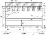
- FIG. 1 is a schematic plan view of a semiconductor device according to a first embodiment.
- FIG. 2 is a cross-sectional view taken along line II-II in FIG. It is a schematic diagram which shows the state of the electron which flows into the collector layer in a recovery state, and the hole inject
- a first embodiment will be described with reference to the drawings. Note that the semiconductor device of this embodiment is preferably used as a power switching element used in a power supply circuit such as an inverter or a DC / DC converter.
- the semiconductor device is an RC (ie, Reverse Conducting) -IGBT in which an IGBT region 1 having an IGBT element 1a and an FWD region 2 having an FWD element 2a are formed on a common semiconductor substrate 10. It is said that.
- the IGBT regions 1 and the FWD regions 2 extend along one direction and are alternately formed in a direction crossing the extending direction.
- the IGBT region 1 and the FWD region 2 extend along the horizontal direction of the paper surface and are alternately formed in the vertical direction of the paper surface.
- the semiconductor substrate 10 has an N ⁇ type drift layer 11.
- the semiconductor substrate 10 is comprised with a silicon substrate, for example.
- a P-type base layer 12 is formed on the drift layer 11 (that is, on the one surface 10a side of the semiconductor substrate 10).
- a plurality of trenches 13 are formed in the semiconductor substrate 10 so as to penetrate the base layer 12 and reach the drift layer 11. Thereby, the base layer 12 is separated into a plurality by the trench 13.
- the plurality of trenches 13 are formed in the IGBT region 1 and the FWD region 2, respectively, and are formed in stripes formed at equal intervals along one direction of the surface direction of the one surface 10a of the semiconductor substrate 10. ing. In FIG. 2, each trench 13 is formed along the direction perpendicular to the paper surface.
- Each trench 13 is embedded with a gate insulating film 14 formed so as to cover the wall surface of each trench 13 and a gate electrode 15 made of polysilicon or the like formed on the gate insulating film 14. . Thereby, a trench gate structure is configured.
- An N + -type emitter region 16 having a higher impurity concentration than that of the drift layer 11 is formed in the surface layer portion of the base layer 12 (that is, the one surface 10 a side of the semiconductor substrate 10). Specifically, the emitter region 16 is formed so as to terminate in the base layer 12 and to be in contact with the side surface of the trench 13. More specifically, the emitter region 16 extends in a rod shape so as to be in contact with the side surface of the trench 13 along the longitudinal direction of the trench 13 in the region between the trenches 13 and terminates inside the tip of the trench 13.
- the portion of the wall surface of the trench 13 located between the emitter region 16 and the drift layer 11 corresponds to the surface of the base layer located between the emitter region and the drift layer.
- An interlayer insulating film 17 made of BPSG (ie, Boron Phosphorus Silicon Glass) or the like is formed on one surface 10a of the semiconductor substrate 10.
- An upper electrode 18 electrically connected to the emitter region 16 and the base layer 12 is formed on the interlayer insulating film 17 through a contact hole 17 a formed in the interlayer insulating film 17. That is, an upper electrode 18 that functions as an emitter electrode in the IGBT region 1 and functions as an anode electrode in the FWD region 2 is formed on the interlayer insulating film 17.
- the upper electrode 18 corresponds to the first electrode.
- a plurality of pad portions 19 connected to the gate electrode 15, a temperature sensor (not shown), and the like are formed on one surface 10 a of the semiconductor substrate 10.
- a P + -type collector layer 20 is formed on the drift layer 11 on the side opposite to the base layer 12 side (that is, the other surface 10 b side) of the drift layer 11.
- an N + -type cathode layer 21 is formed on the side of the drift layer 11 opposite to the base layer 12 side (that is, the other surface 10 b side of the semiconductor substrate 10). That is, the IGBT region 1 and the FWD region 2 are partitioned depending on whether the layer formed on the other surface 10 b side of the semiconductor substrate 10 is the collector layer 20 or the cathode layer 21.
- the portion on the collector layer 20 is the IGBT region 1 and the portion on the cathode layer 21 is the FWD region 2.
- the collector layer 20 and the cathode layer 21 are formed to the same depth from the other surface 10b of the semiconductor substrate 10 toward the one surface 10a.
- an N-type FS layer 22 having a higher impurity concentration than the drift layer 11 is formed on the drift layer 11 on the side opposite to the base layer 12 side (that is, the other surface 10b side of the semiconductor substrate 10).
- the FS layer 22 is formed at a position away from the collector layer 20 and the cathode layer 21.
- the FS layer 22 is formed in the drift layer 11. That is, the FS layer 22 is formed so that a part of the drift layer 11 remains between the collector layer 20 and the cathode layer 21.
- the FS layer 22 is formed such that the ratio of the distance L2 between the FS layer 22, the collector layer 20, and the cathode layer 21 to the thickness L1 of the semiconductor substrate 10 is a predetermined value. Yes.
- a lower electrode 23 electrically connected to the collector layer 20 and the cathode layer 21 is formed on the opposite side of the drift layer 11 (that is, the other surface 10b of the semiconductor substrate 10) with the collector layer 20 and the cathode layer 21 interposed therebetween. ing. That is, the lower electrode 23 that functions as a collector electrode in the IGBT region 1 and functions as a cathode electrode in the FWD region 2 is formed. In the present embodiment, the lower electrode 23 corresponds to the second electrode.
- the FWD region 2 includes the FWD element 2a that is PN-junctioned with the base layer 12 as an anode and the drift layer 11, the FS layer 22, and the cathode layer 21 as a cathode. ing.
- the N type, N + type, and N ⁇ type correspond to the first conductivity type
- the P type and P + type correspond to the second conductivity type
- the semiconductor substrate 10 includes the collector layer 20, the cathode layer 21, the drift layer 11, the FS layer 22, the base layer 12, and the emitter region 16 as described above. Next, the operation of the semiconductor device will be described.
- the semiconductor device when a voltage higher than that of the upper electrode 18 is applied to the lower electrode 23, the PN junction formed between the base layer 12 and the drift layer 11 is in a reverse conducting state, and a depletion layer is formed. The At this time, no current flows between the upper electrode 18 and the lower electrode 23 when a low level (for example, 0 V) voltage lower than the threshold voltage Vth of the insulated gate structure is applied to the gate electrode 15.
- a low level for example, 0 V
- a high level voltage equal to or higher than the threshold voltage Vth of the insulated gate structure is applied to the gate electrode 15 while a voltage higher than that of the upper electrode 18 is applied to the lower electrode 23.
- an inversion layer is formed in a portion of the base layer 12 that is in contact with the trench 13.
- electrons are supplied from the emitter region 16 to the drift layer 11 through the inversion layer, whereby holes are supplied from the collector layer 20 to the drift layer 11, and the resistance of the drift layer 11 is controlled by conductivity modulation. When the value decreases, it is turned on.
- the IGBT element 1a is turned off and the FWD element 2a is turned on (that is, the FWD element 2a is diode-operated)
- the voltage applied to the upper electrode 18 and the lower electrode 23 is switched, and the upper electrode A voltage higher than that of the lower electrode 23 is applied to 18.
- a low level voltage for example, 0 V
- the threshold voltage Vth of the insulated gate structure is applied to the gate electrode 15.
- the inversion layer is not formed in the portion of the base layer 12 in contact with the trench 13, holes are supplied from the upper electrode 18 through the base layer 12, and from the lower electrode 23 through the cathode layer 21. Electrons are supplied, and the FWD element 2a operates as a diode.
- a reverse voltage is applied to the lower electrode 23 to apply a voltage higher than that of the upper electrode 18. That is, when the current is cut off from a state in which a forward current flows through the FWD element 2a, reverse voltage application is performed to apply a voltage higher than that of the upper electrode 18 to the lower electrode 23. As a result, the FWD element 2a enters a recovery state. Then, holes in the base layer 12 are attracted to the upper electrode 18 side, and electrons in the drift layer 11 are attracted to the lower electrode 23 side, so that a recovery current is generated, and the gap between the base layer 12 and the drift layer 11 is generated. The depletion layer grows.
- the FS layer 22 is formed away from the collector layer 20 and the cathode layer 21. Therefore, in the semiconductor device of this embodiment, the internal resistance of the region located on and near the collector layer 20 is higher than that of the conventional semiconductor device in which the FS layer 22 is in contact with the collector layer 20 and the cathode layer 21. growing. For this reason, in the semiconductor device of this embodiment, the voltage drop when electrons flow into the collector layer 20 is larger than that in the conventional semiconductor device. That is, in the semiconductor device of this embodiment, the potential of the region on the collector layer 20 and in the vicinity thereof is likely to be lower than that of the conventional semiconductor device.
- the semiconductor device of this embodiment in the recovery state, electrons easily flow into the collector layer 20, and accordingly, the amount of holes injected into the drift layer 11 via the collector layer 20 increases. Then, since holes injected from the collector layer 20 spread along the surface direction of the semiconductor substrate 10, the holes are also supplied to the region on the cathode layer 21. For this reason, in the semiconductor device of this embodiment, in the recovery state, carriers are not easily depleted in the FWD region 2, and the depletion layer is difficult to extend to the other surface 10 b side of the semiconductor substrate 10. That is, in the semiconductor device of this embodiment, in the recovery state, the space charge density of the FWD region 2 is increased, and the depletion layer is difficult to extend to the other surface 10 b side of the semiconductor substrate 10. Thereby, in the semiconductor device of this embodiment, complete depletion can be suppressed and the surge peak voltage can be reduced in the recovery state.
- electrons correspond to first carriers and holes correspond to second carriers.
- the FS layer 22 of the present embodiment is formed at a position where an appropriate amount of holes with a reduced surge peak voltage is injected in the recovery state.
- the inventors further examined the magnitude of the surge peak voltage and the ratio of the distance L2 between the FS layer 22, the collector layer 20, and the cathode layer 21 with respect to the thickness L1 of the semiconductor substrate 10, and FIG. The results shown are obtained.
- the thickness L1 of the semiconductor substrate 10 is the length between the one surface 10a and the other surface 10b of the semiconductor substrate 10.
- the distance L2 between the FS layer 22, the collector layer 20, and the cathode layer 21 is the length along the thickness direction of the semiconductor substrate 10 between the FS layer 22, the collector layer 20, and the cathode layer 21.
- the distance L ⁇ b> 2 between the FS layer 22, the collector layer 20, and the cathode layer 21 is simply indicated as the distance between the FS layers 22.
- the ratio [%] of the distance L2 between the FS layer 22, the collector layer 20, and the cathode layer 21 with respect to the thickness L1 of the semiconductor substrate 10 is simply referred to as L2 / L1.
- the surge peak voltage decreases as L2 / L1 is gradually increased from 0.
- the case where L2 / L1 is 0 is a case where the FS layer 22 is in contact with the collector layer 20 and the cathode layer 21.
- the surge peak voltage is almost equal when L2 / L1 is 2 to 17%. Further, the surge peak voltage is sharply reduced when L2 / L1 is further increased from 17%, and is minimized when L2 / L1 is about 19%. The surge peak voltage sharply decreases when L2 / L1 is between 17% and 19% because the number of holes injected into the drift layer 11 increases, so that the constant voltage is reached when the surge peak voltage is reached. This is because the sustain voltage up to the time point increases.
- the surge peak voltage gradually increases when L2 / L1 is greater than 19%, and becomes the same magnitude as when L1 / L2 is 0 when L2 / L1 is 21.5%. .
- the surge peak voltage further increases when L2 / L1 is made larger than 21.5%.
- the reason why the surge peak voltage is further increased when L2 / L1 is made larger than 21.5% is that holes are excessively injected when L2 / L1 becomes too large, and the sustain voltage becomes too large. That is, if the distance L2 between the FS layer 22, the collector layer 20 and the cathode layer 21 becomes too large, the surge peak voltage will increase.
- the FS layer 22 is formed at a position where L2 / L1 is less than 21.5% so that an appropriate amount of holes with a small surge peak voltage is injected. More specifically, the FS layer 22 is preferably formed so that L2 / L1 is 2 to 19% so that the surge peak voltage is stably reduced.
- the thickness of the semiconductor substrate 10 is 80 ⁇ m
- the impurity concentration of the drift layer 11 is 1.0 ⁇ 10 14 cm ⁇ 3
- the impurity concentration of the FS layer 22 is 1.0 ⁇ 10 16 cm ⁇ 3
- the base This is a simulation result when the impurity concentration of the layer 12 is 2.5 ⁇ 10 17 cm ⁇ 3 and the impurity concentration of the cathode layer 21 is 5.0 ⁇ 10 19 cm ⁇ 3 .
- the semiconductor device of this embodiment can reduce the surge peak voltage regardless of the impurity concentration or the like by forming the FS layer 22 so that L2 / L1 is less than 21.5%.
- the FS layer 22 is formed at a position away from the collector layer 20 and the cathode layer 21.
- an appropriate amount of holes is injected from the collector layer 20 into the drift layer 11 so that the surge peak voltage can be reduced. That is, L1 / L2 is set to be less than 21.5%. For this reason, a surge peak voltage can be made small and it can suppress that a semiconductor device is destroyed.
- a plurality of P + type carrier injection layers 24 are formed in the cathode layer 21.
- the plurality of carrier injection layers 24 are formed in a stripe shape along the extending direction of the cathode layer 21.
- the holes in the drift layer 11 flow into the carrier injection layer 24 located in the cathode layer 21 together with the collector layer 20. Then, holes are also injected into the drift layer 11 via the carrier injection layer 24. For this reason, in the recovery state, the carriers are more difficult to be depleted in the FWD region 2, and the surge peak voltage can be reduced.
- the FS layer 22 is formed at a position where the distance L2 between the collector layer 20 and the cathode layer 21 is adjusted so that an appropriate amount of holes for reducing the surge peak voltage is injected.
- the first conductivity type is N type and the second conductivity type is P type has been described.
- the first conductivity type is P type
- the second conductivity type is N type.
- a P + -type contact region having a higher impurity concentration than that of the base layer 12 is formed on the surface layer portion of the base layer 12 (that is, on the one surface 10a side of the semiconductor substrate 10). Also good.
- a plurality of FS layers 22 may be formed in the thickness direction of the semiconductor substrate 10.
- two FS layers 22 may be formed along the thickness direction of the semiconductor substrate 10.
- the distance L2 between the FS layer 22 located closest to the other surface 10b of the semiconductor substrate 10 and the collector layer 20 and the cathode layer 21 is such that an appropriate amount of holes that reduce the surge peak voltage is injected. It may be adjusted so as to be the same as in the first embodiment.
- a trench gate type semiconductor device not a trench gate type semiconductor device but a planar type semiconductor device in which the gate electrode 15 is disposed on the one surface 10a of the semiconductor substrate 10 may be used.
- the gate electrode 15 since the gate electrode 15 is disposed on the one surface 10a of the semiconductor substrate 10 via the gate insulating film 14, a portion of the base layer 12 constituting the one surface 10a of the semiconductor substrate 10 is on the surface of the base layer. Equivalent to.
- the plurality of carrier injection layers 24 may be formed in a lattice shape, for example, instead of a stripe shape. Moreover, the carrier injection layer 24 may be formed only one instead of plural.
Landscapes
- Metal-Oxide And Bipolar Metal-Oxide Semiconductor Integrated Circuits (AREA)
Applications Claiming Priority (2)
| Application Number | Priority Date | Filing Date | Title |
|---|---|---|---|
| JP2017117072A JP2019004030A (ja) | 2017-06-14 | 2017-06-14 | 半導体装置 |
| JP2017-117072 | 2017-06-14 |
Publications (1)
| Publication Number | Publication Date |
|---|---|
| WO2018230312A1 true WO2018230312A1 (ja) | 2018-12-20 |
Family
ID=64660825
Family Applications (1)
| Application Number | Title | Priority Date | Filing Date |
|---|---|---|---|
| PCT/JP2018/020231 Ceased WO2018230312A1 (ja) | 2017-06-14 | 2018-05-25 | 半導体装置 |
Country Status (2)
| Country | Link |
|---|---|
| JP (1) | JP2019004030A (enExample) |
| WO (1) | WO2018230312A1 (enExample) |
Families Citing this family (1)
| Publication number | Priority date | Publication date | Assignee | Title |
|---|---|---|---|---|
| JP7409326B2 (ja) | 2019-01-15 | 2024-01-09 | ソニーグループ株式会社 | サーバおよび学習システム |
Citations (6)
| Publication number | Priority date | Publication date | Assignee | Title |
|---|---|---|---|---|
| WO2007055352A1 (ja) * | 2005-11-14 | 2007-05-18 | Fuji Electric Device Technology Co., Ltd. | 半導体装置およびその製造方法 |
| JP2013065735A (ja) * | 2011-09-19 | 2013-04-11 | Denso Corp | 半導体装置 |
| JP2015177057A (ja) * | 2014-03-14 | 2015-10-05 | 株式会社東芝 | 半導体装置 |
| JP2015213193A (ja) * | 2015-07-21 | 2015-11-26 | ルネサスエレクトロニクス株式会社 | Igbt |
| JP2016006891A (ja) * | 2011-07-27 | 2016-01-14 | トヨタ自動車株式会社 | ダイオード、半導体装置およびmosfet |
| EP3154091A1 (en) * | 2015-10-07 | 2017-04-12 | ABB Technology AG | Reverse-conducting semiconductor device |
Family Cites Families (4)
| Publication number | Priority date | Publication date | Assignee | Title |
|---|---|---|---|---|
| JP2012142537A (ja) * | 2010-12-16 | 2012-07-26 | Mitsubishi Electric Corp | 絶縁ゲート型バイポーラトランジスタとその製造方法 |
| JP5751125B2 (ja) * | 2011-10-20 | 2015-07-22 | 株式会社デンソー | 半導体装置 |
| JP6119577B2 (ja) * | 2013-11-26 | 2017-04-26 | 三菱電機株式会社 | 半導体装置 |
| JP6261494B2 (ja) * | 2014-12-03 | 2018-01-17 | 三菱電機株式会社 | 電力用半導体装置 |
-
2017
- 2017-06-14 JP JP2017117072A patent/JP2019004030A/ja active Pending
-
2018
- 2018-05-25 WO PCT/JP2018/020231 patent/WO2018230312A1/ja not_active Ceased
Patent Citations (6)
| Publication number | Priority date | Publication date | Assignee | Title |
|---|---|---|---|---|
| WO2007055352A1 (ja) * | 2005-11-14 | 2007-05-18 | Fuji Electric Device Technology Co., Ltd. | 半導体装置およびその製造方法 |
| JP2016006891A (ja) * | 2011-07-27 | 2016-01-14 | トヨタ自動車株式会社 | ダイオード、半導体装置およびmosfet |
| JP2013065735A (ja) * | 2011-09-19 | 2013-04-11 | Denso Corp | 半導体装置 |
| JP2015177057A (ja) * | 2014-03-14 | 2015-10-05 | 株式会社東芝 | 半導体装置 |
| JP2015213193A (ja) * | 2015-07-21 | 2015-11-26 | ルネサスエレクトロニクス株式会社 | Igbt |
| EP3154091A1 (en) * | 2015-10-07 | 2017-04-12 | ABB Technology AG | Reverse-conducting semiconductor device |
Also Published As
| Publication number | Publication date |
|---|---|
| JP2019004030A (ja) | 2019-01-10 |
Similar Documents
| Publication | Publication Date | Title |
|---|---|---|
| US10170607B2 (en) | Semiconductor device | |
| JP6589817B2 (ja) | 半導体装置 | |
| US10062760B2 (en) | Semiconductor device | |
| JP5787853B2 (ja) | 電力用半導体装置 | |
| JP2017208413A (ja) | 半導体装置 | |
| JPWO2018220879A1 (ja) | 半導体装置 | |
| WO2017155122A1 (ja) | 半導体装置 | |
| JP5480084B2 (ja) | 半導体装置 | |
| JP2016136620A (ja) | 半導体装置 | |
| JP2008053648A (ja) | 絶縁ゲート型半導体装置及びその製造方法 | |
| WO2013065247A1 (ja) | 半導体装置 | |
| JP2007184486A (ja) | 半導体装置 | |
| JP2016157934A (ja) | 半導体装置 | |
| JP2013235891A (ja) | 半導体装置 | |
| JP2013080796A (ja) | 半導体装置 | |
| CN112673466A (zh) | 半导体装置 | |
| JP5537359B2 (ja) | 半導体装置 | |
| JP2020177973A (ja) | 半導体装置 | |
| US20150357450A1 (en) | Charge reservoir igbt top structure | |
| US20170309704A1 (en) | Semiconductor device and manufacturing method therefor | |
| JP6935731B2 (ja) | 半導体装置 | |
| JP6624101B2 (ja) | 半導体装置 | |
| US20150187919A1 (en) | Power semiconductor device | |
| WO2018198575A1 (ja) | 半導体装置 | |
| JP2014154739A (ja) | 半導体装置 |
Legal Events
| Date | Code | Title | Description |
|---|---|---|---|
| 121 | Ep: the epo has been informed by wipo that ep was designated in this application |
Ref document number: 18816891 Country of ref document: EP Kind code of ref document: A1 |
|
| NENP | Non-entry into the national phase |
Ref country code: DE |
|
| 122 | Ep: pct application non-entry in european phase |
Ref document number: 18816891 Country of ref document: EP Kind code of ref document: A1 |