WO2018180224A1 - Procédé de nettoyage d'une tranche de semi-conducteur - Google Patents
Procédé de nettoyage d'une tranche de semi-conducteur Download PDFInfo
- Publication number
- WO2018180224A1 WO2018180224A1 PCT/JP2018/008197 JP2018008197W WO2018180224A1 WO 2018180224 A1 WO2018180224 A1 WO 2018180224A1 JP 2018008197 W JP2018008197 W JP 2018008197W WO 2018180224 A1 WO2018180224 A1 WO 2018180224A1
- Authority
- WO
- WIPO (PCT)
- Prior art keywords
- semiconductor wafer
- ozone water
- cleaning
- hydrofluoric acid
- speed
- Prior art date
Links
- 239000004065 semiconductor Substances 0.000 title claims abstract description 90
- 238000004140 cleaning Methods 0.000 title claims abstract description 61
- 238000000034 method Methods 0.000 title claims abstract description 29
- XLYOFNOQVPJJNP-UHFFFAOYSA-N water Substances O XLYOFNOQVPJJNP-UHFFFAOYSA-N 0.000 claims abstract description 81
- CBENFWSGALASAD-UHFFFAOYSA-N Ozone Chemical compound [O-][O+]=O CBENFWSGALASAD-UHFFFAOYSA-N 0.000 claims abstract description 79
- KRHYYFGTRYWZRS-UHFFFAOYSA-N Fluorane Chemical compound F KRHYYFGTRYWZRS-UHFFFAOYSA-N 0.000 claims abstract description 78
- 238000003780 insertion Methods 0.000 claims abstract description 24
- 230000037431 insertion Effects 0.000 claims abstract description 24
- XUIMIQQOPSSXEZ-UHFFFAOYSA-N Silicon Chemical compound [Si] XUIMIQQOPSSXEZ-UHFFFAOYSA-N 0.000 claims description 11
- 229910052710 silicon Inorganic materials 0.000 claims description 11
- 239000010703 silicon Substances 0.000 claims description 11
- 239000002245 particle Substances 0.000 abstract description 34
- 238000007654 immersion Methods 0.000 abstract description 8
- 235000012431 wafers Nutrition 0.000 description 86
- 239000007788 liquid Substances 0.000 description 7
- 239000000126 substance Substances 0.000 description 6
- QGZKDVFQNNGYKY-UHFFFAOYSA-N Ammonia Chemical compound N QGZKDVFQNNGYKY-UHFFFAOYSA-N 0.000 description 4
- 230000000052 comparative effect Effects 0.000 description 4
- 238000001035 drying Methods 0.000 description 3
- 238000005259 measurement Methods 0.000 description 3
- 238000007254 oxidation reaction Methods 0.000 description 3
- 229910021529 ammonia Inorganic materials 0.000 description 2
- 230000015572 biosynthetic process Effects 0.000 description 2
- 238000003795 desorption Methods 0.000 description 2
- 230000005661 hydrophobic surface Effects 0.000 description 2
- QPJSUIGXIBEQAC-UHFFFAOYSA-N n-(2,4-dichloro-5-propan-2-yloxyphenyl)acetamide Chemical compound CC(C)OC1=CC(NC(C)=O)=C(Cl)C=C1Cl QPJSUIGXIBEQAC-UHFFFAOYSA-N 0.000 description 2
- 230000003647 oxidation Effects 0.000 description 2
- 230000000630 rising effect Effects 0.000 description 2
- 239000000758 substrate Substances 0.000 description 2
- 238000005406 washing Methods 0.000 description 2
- MHAJPDPJQMAIIY-UHFFFAOYSA-N Hydrogen peroxide Chemical compound OO MHAJPDPJQMAIIY-UHFFFAOYSA-N 0.000 description 1
- 230000002411 adverse Effects 0.000 description 1
- 230000007423 decrease Effects 0.000 description 1
- 238000007598 dipping method Methods 0.000 description 1
- 230000000694 effects Effects 0.000 description 1
- 238000011835 investigation Methods 0.000 description 1
- 239000000463 material Substances 0.000 description 1
- 230000001590 oxidative effect Effects 0.000 description 1
- 238000000926 separation method Methods 0.000 description 1
Images


Classifications
-
- H—ELECTRICITY
- H01—ELECTRIC ELEMENTS
- H01L—SEMICONDUCTOR DEVICES NOT COVERED BY CLASS H10
- H01L21/00—Processes or apparatus adapted for the manufacture or treatment of semiconductor or solid state devices or of parts thereof
- H01L21/02—Manufacture or treatment of semiconductor devices or of parts thereof
- H01L21/02041—Cleaning
- H01L21/02043—Cleaning before device manufacture, i.e. Begin-Of-Line process
- H01L21/02052—Wet cleaning only
-
- H—ELECTRICITY
- H01—ELECTRIC ELEMENTS
- H01L—SEMICONDUCTOR DEVICES NOT COVERED BY CLASS H10
- H01L21/00—Processes or apparatus adapted for the manufacture or treatment of semiconductor or solid state devices or of parts thereof
- H01L21/02—Manufacture or treatment of semiconductor devices or of parts thereof
- H01L21/02041—Cleaning
- H01L21/02057—Cleaning during device manufacture
-
- B—PERFORMING OPERATIONS; TRANSPORTING
- B08—CLEANING
- B08B—CLEANING IN GENERAL; PREVENTION OF FOULING IN GENERAL
- B08B3/00—Cleaning by methods involving the use or presence of liquid or steam
- B08B3/04—Cleaning involving contact with liquid
- B08B3/08—Cleaning involving contact with liquid the liquid having chemical or dissolving effect
-
- C—CHEMISTRY; METALLURGY
- C11—ANIMAL OR VEGETABLE OILS, FATS, FATTY SUBSTANCES OR WAXES; FATTY ACIDS THEREFROM; DETERGENTS; CANDLES
- C11D—DETERGENT COMPOSITIONS; USE OF SINGLE SUBSTANCES AS DETERGENTS; SOAP OR SOAP-MAKING; RESIN SOAPS; RECOVERY OF GLYCEROL
- C11D7/00—Compositions of detergents based essentially on non-surface-active compounds
- C11D7/02—Inorganic compounds
- C11D7/04—Water-soluble compounds
- C11D7/08—Acids
-
- H—ELECTRICITY
- H01—ELECTRIC ELEMENTS
- H01L—SEMICONDUCTOR DEVICES NOT COVERED BY CLASS H10
- H01L21/00—Processes or apparatus adapted for the manufacture or treatment of semiconductor or solid state devices or of parts thereof
- H01L21/02—Manufacture or treatment of semiconductor devices or of parts thereof
- H01L21/04—Manufacture or treatment of semiconductor devices or of parts thereof the devices having at least one potential-jump barrier or surface barrier, e.g. PN junction, depletion layer or carrier concentration layer
- H01L21/18—Manufacture or treatment of semiconductor devices or of parts thereof the devices having at least one potential-jump barrier or surface barrier, e.g. PN junction, depletion layer or carrier concentration layer the devices having semiconductor bodies comprising elements of Group IV of the Periodic System or AIIIBV compounds with or without impurities, e.g. doping materials
- H01L21/30—Treatment of semiconductor bodies using processes or apparatus not provided for in groups H01L21/20 - H01L21/26
- H01L21/302—Treatment of semiconductor bodies using processes or apparatus not provided for in groups H01L21/20 - H01L21/26 to change their surface-physical characteristics or shape, e.g. etching, polishing, cutting
- H01L21/304—Mechanical treatment, e.g. grinding, polishing, cutting
-
- H—ELECTRICITY
- H01—ELECTRIC ELEMENTS
- H01L—SEMICONDUCTOR DEVICES NOT COVERED BY CLASS H10
- H01L21/00—Processes or apparatus adapted for the manufacture or treatment of semiconductor or solid state devices or of parts thereof
- H01L21/67—Apparatus specially adapted for handling semiconductor or electric solid state devices during manufacture or treatment thereof; Apparatus specially adapted for handling wafers during manufacture or treatment of semiconductor or electric solid state devices or components ; Apparatus not specifically provided for elsewhere
- H01L21/67005—Apparatus not specifically provided for elsewhere
- H01L21/67011—Apparatus for manufacture or treatment
- H01L21/67017—Apparatus for fluid treatment
- H01L21/67028—Apparatus for fluid treatment for cleaning followed by drying, rinsing, stripping, blasting or the like
- H01L21/6704—Apparatus for fluid treatment for cleaning followed by drying, rinsing, stripping, blasting or the like for wet cleaning or washing
- H01L21/67057—Apparatus for fluid treatment for cleaning followed by drying, rinsing, stripping, blasting or the like for wet cleaning or washing with the semiconductor substrates being dipped in baths or vessels
-
- C11D2111/22—
-
- H—ELECTRICITY
- H01—ELECTRIC ELEMENTS
- H01L—SEMICONDUCTOR DEVICES NOT COVERED BY CLASS H10
- H01L2924/00—Indexing scheme for arrangements or methods for connecting or disconnecting semiconductor or solid-state bodies as covered by H01L24/00
- H01L2924/01—Chemical elements
- H01L2924/01009—Fluorine [F]
-
- Y—GENERAL TAGGING OF NEW TECHNOLOGICAL DEVELOPMENTS; GENERAL TAGGING OF CROSS-SECTIONAL TECHNOLOGIES SPANNING OVER SEVERAL SECTIONS OF THE IPC; TECHNICAL SUBJECTS COVERED BY FORMER USPC CROSS-REFERENCE ART COLLECTIONS [XRACs] AND DIGESTS
- Y02—TECHNOLOGIES OR APPLICATIONS FOR MITIGATION OR ADAPTATION AGAINST CLIMATE CHANGE
- Y02P—CLIMATE CHANGE MITIGATION TECHNOLOGIES IN THE PRODUCTION OR PROCESSING OF GOODS
- Y02P70/00—Climate change mitigation technologies in the production process for final industrial or consumer products
- Y02P70/50—Manufacturing or production processes characterised by the final manufactured product
Definitions
- the present invention relates to a method for cleaning a semiconductor wafer.
- the immersion (insertion) speed into the ozone water tank is conventionally fixed and is not changed. The speed was as low as about 10,000 mm / min.
- the present invention has been made in view of the above problems, and in the method of cleaning a semiconductor wafer by immersing it in hydrofluoric acid and then immersing it in ozone water, cleaning and removing foreign matters such as particles. It is an object of the present invention to provide a method for cleaning a semiconductor wafer that can prevent reattachment of foreign matters.
- the present invention inserts a semiconductor wafer into a hydrofluoric acid tank filled with hydrofluoric acid, immerses it in the hydrofluoric acid, pulls it out from the hydrofluoric acid tank,
- the semiconductor wafer cleaning method is characterized in that the insertion speed is set to 20000 mm / min or more until the semiconductor wafer is completely immersed in the ozone water after the lower end of the substrate contacts the ozone water.
- Such a method for cleaning a semiconductor wafer can prevent foreign matters such as particles from remaining and reattachment of removed foreign matters.
- the transport speed is increased, the throughput is improved.
- the insertion of the semiconductor wafer into the ozone water tank is performed such that the lower end of the semiconductor wafer is in contact with the ozone water, and the upper end of the semiconductor wafer is at a position of 50 mm or more from the liquid level of the ozone water. Until it becomes, it is preferable to perform insertion speed as 20000 mm / min or more.
- the cleaning method of the present invention is particularly effective when cleaning a silicon wafer.
- the semiconductor wafer is immersed in hydrofluoric acid to remove the natural oxide film, and then immersed in ozone water to form a natural oxide film. It is possible to prevent reattachment of the remaining or removed foreign matter. Furthermore, it leads to an increase in the conveyance speed, so that the throughput is improved.
- the present inventors have made the insertion of the semiconductor wafer into the ozone water tank at a predetermined insertion speed or higher, so that foreign matters such as particles can remain.
- the present inventors have found that it is possible to prevent reattachment of the removed foreign matter, and have reached the present invention.
- a semiconductor wafer is inserted into a hydrofluoric acid tank filled with hydrofluoric acid, immersed in the hydrofluoric acid, pulled out from the hydrofluoric acid tank, and then filled with ozone water.
- the semiconductor wafer cleaning method is characterized in that the insertion speed is set to 20000 mm / min or more until the semiconductor wafer is completely immersed in ozone water after contacting the substrate.
- the “insertion speed” refers to the relative speed between the semiconductor wafer and the cleaning tank. Specifically, (i) when the semiconductor wafer is pulled down and inserted into the cleaning tank at a predetermined position, Both the semiconductor wafer pulling speed, (ii) the cleaning tank rising speed when the cleaning tank is raised and a semiconductor wafer at a predetermined position is inserted into the cleaning tank, and (iii) the semiconductor wafer pulling down and the cleaning tank rise. It includes both of the semiconductor wafer pulling speed and the cleaning tank rising speed.
- the “drawing speed” also refers to the relative speed between the semiconductor wafer and the cleaning tank.
- FIG. 1 shows a cleaning flow chart showing an example of a semiconductor wafer cleaning method of the present invention.
- the semiconductor wafer to be cleaned is not particularly limited, but a silicon wafer can be used.
- the semiconductor wafer can be rinsed with, for example, ammonia / hydrogen peroxide solution cleaning (SC1 cleaning) or pure water before cleaning with hydrofluoric acid (FIGS. 1A and 1B).
- SC1 cleaning ammonia / hydrogen peroxide solution cleaning
- pure water before cleaning with hydrofluoric acid
- the semiconductor wafer is inserted into a hydrofluoric acid tank filled with hydrofluoric acid and immersed in hydrofluoric acid to perform hydrofluoric acid cleaning (FIG. 1C).
- hydrofluoric acid cleaning the natural oxide film formed on the semiconductor wafer is removed.
- concentration and temperature of hydrofluoric acid are not limited, but the concentration is preferably 0.3 to 3.0% and the temperature is preferably 10 to 30 ° C.
- the lower limit of the drawing speed is not particularly limited, and can be a speed exceeding 0 mm / min.
- the semiconductor wafer is inserted into an ozone water tank filled with ozone water and immersed in ozone water for cleaning (FIG. 1D).
- FIG. 2 is a schematic view showing a process of inserting a semiconductor wafer into an ozone water tank.
- the semiconductor wafer 1 when the semiconductor wafer 1 is inserted into the ozone water tank 3 filled with the ozone water 2, at least the lower end of the semiconductor wafer 1 comes into contact with the ozone water 2 (FIG. 2A).
- the insertion speed is 20000 mm / min or more until the semiconductor wafer 1 is completely immersed in the ozone water 2 (FIG. 2B).
- the upper limit of the insertion speed is not particularly limited, but usually 50000 mm / min is the apparatus limit.
- the semiconductor wafer 1 from which the natural oxide film has been removed by washing in a hydrofluoric acid bath has a bare surface (hydrophobic surface), and therefore, foreign substances such as particles are very easily attached to the semiconductor wafer 1. There is also a large amount of foreign matter adhering to the surface.
- the insertion speed of the semiconductor wafer 1 is increased to 20000 mm / min or more as in the present invention, the desorption of particles from the semiconductor wafer 1 is efficiently performed, and the semiconductor wafer 1 is quickly submerged in the ozone water tank 3. Therefore, the reattachment of particles near the liquid surface (tank interface) is reduced, and a high-quality wafer can be obtained. In addition, since the transport speed is increased, the throughput is improved.
- the upper end of the semiconductor wafer 1 is at a position of 50 mm or more from the liquid surface of the ozone water 2 (see FIG. 2 (C)), it is preferable to insert the semiconductor wafer 1 into the ozone water tank 3 at an insertion speed of 20000 mm / min or more.
- the position of the upper end of the semiconductor wafer 1 in FIG. 2C can be set to 200 mm or less from the surface of the ozone water 2.
- the semiconductor wafer 1 inserted into the ozone water tank 3 as described above is immersed in the ozone water 2 while being held by the wafer holder 4 (FIG. 2 (D)).
- the concentration of ozone water is preferably 1 ppm or more, the temperature of ozone water is preferably 10 to 30 ° C., and the preferred cleaning time is 60 to 300 seconds.
- the drawing speed at this time is not particularly limited, and can be 1000 mm / min or less.
- treatment such as drying (FIG. 1E) may be performed as appropriate.
- the insertion speed of the semiconductor wafer is not adversely affected by increasing the speed, and it is expected that the reattachment of particles and the like will be suppressed and the throughput will be improved. Therefore, it is desirable that the insertion speed of all the tanks is high, for example, 20000 mm / min or more.
- Examples 1 to 6, Comparative Examples 1 to 4 Using a silicon wafer having a diameter of 300 mm, dip cleaning was performed in the order of ammonia / overwater cleaning ⁇ pure water rinsing ⁇ hydrofluoric acid cleaning ⁇ ozone water cleaning, followed by drying. At that time, the insertion speed of the silicon wafer into the ozone water tank is shown in Table 1 until the lower end of the silicon wafer comes into contact with the ozone water until the upper end of the silicon wafer is positioned 50 mm from the surface of the ozone water. Done as a speed. The insertion speed into tanks other than the ozone water tank was 15000 mm / min, and the drawing speed from all tanks was 1000 mm / min.
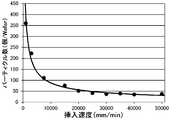
- FIG. 3 shows the relationship between the insertion speed of the silicon wafer into the ozone water tank and the particle measurement results.
- the number of particles on the silicon wafer decreases as the immersion rate in the ozone water bath increases and the insertion rate is 20000 mm / min (Example 1) or more. It was found that the number of particles on the wafer converged and became almost constant. That is, in Examples 1 to 6, the number of particles on the wafer was improved and the quality of the wafer was improved.
- the present invention is not limited to the above embodiment.
- the above-described embodiment is an exemplification, and the present invention has substantially the same configuration as the technical idea described in the claims of the present invention, and any device that exhibits the same function and effect is the present invention. It is included in the technical scope of the invention.
Landscapes
- Engineering & Computer Science (AREA)
- Physics & Mathematics (AREA)
- Condensed Matter Physics & Semiconductors (AREA)
- General Physics & Mathematics (AREA)
- Manufacturing & Machinery (AREA)
- Computer Hardware Design (AREA)
- Microelectronics & Electronic Packaging (AREA)
- Power Engineering (AREA)
- Chemical & Material Sciences (AREA)
- Chemical Kinetics & Catalysis (AREA)
- General Chemical & Material Sciences (AREA)
- Inorganic Chemistry (AREA)
- Life Sciences & Earth Sciences (AREA)
- Oil, Petroleum & Natural Gas (AREA)
- Wood Science & Technology (AREA)
- Organic Chemistry (AREA)
- Cleaning Or Drying Semiconductors (AREA)
Abstract
La présente invention concerne un procédé de nettoyage d'une tranche de semi-conducteur dans lequel : une tranche de semi-conducteur est introduite dans un réservoir d'acide fluorhydrique rempli d'acide fluorhydrique, immergée dans l'acide fluorhydrique et extraite du réservoir d'acide fluorhydrique ; et la tranche de semi-conducteur est ensuite introduite dans un réservoir d'eau ozonisée rempli d'eau ozonisée, immergée dans l'eau ozonisée et nettoyée, le procédé étant caractérisé en ce que l'introduction de la tranche de semi-conducteur dans le réservoir d'eau ozonisée est effectuée à une vitesse d'introduction de 20 000 mm/min ou plus au moins depuis le moment où l'extrémité inférieure de la tranche de semi-conducteur entre en contact avec l'eau ozonisée jusqu'au moment où la tranche de semi-conducteur est complètement immergée dans l'eau ozonisée. Il est ainsi proposé un procédé de nettoyage d'une tranche de semi-conducteur au moyen duquel il est possible d'empêcher des particules et d'autres matières étrangères de rester sur une tranche de semi-conducteur et d'empêcher les matières étrangères retirées de re-adhérer à ladite tranche dans un procédé de nettoyage dans lequel la tranche de semi-conducteur est nettoyée par immersion dans de l'acide fluorhydrique et ensuite nettoyée par immersion dans de l'eau ozonisée.
Priority Applications (5)
| Application Number | Priority Date | Filing Date | Title |
|---|---|---|---|
| CN201880019193.1A CN110447088B (zh) | 2017-03-29 | 2018-03-05 | 半导体晶圆的清洗方法 |
| DE112018001115.1T DE112018001115T5 (de) | 2017-03-29 | 2018-03-05 | Verfahren zum Reinigen eines Halbleiterwafers |
| US16/491,294 US11177125B2 (en) | 2017-03-29 | 2018-03-05 | Method for cleaning semiconductor wafer |
| SG11201908278R SG11201908278RA (en) | 2017-03-29 | 2018-03-05 | Method for cleaning semiconductor wafer |
| KR1020197027585A KR102466269B1 (ko) | 2017-03-29 | 2018-03-05 | 반도체 웨이퍼의 세정방법 |
Applications Claiming Priority (2)
| Application Number | Priority Date | Filing Date | Title |
|---|---|---|---|
| JP2017-065628 | 2017-03-29 | ||
| JP2017065628A JP6686955B2 (ja) | 2017-03-29 | 2017-03-29 | 半導体ウェーハの洗浄方法 |
Publications (1)
| Publication Number | Publication Date |
|---|---|
| WO2018180224A1 true WO2018180224A1 (fr) | 2018-10-04 |
Family
ID=63675389
Family Applications (1)
| Application Number | Title | Priority Date | Filing Date |
|---|---|---|---|
| PCT/JP2018/008197 WO2018180224A1 (fr) | 2017-03-29 | 2018-03-05 | Procédé de nettoyage d'une tranche de semi-conducteur |
Country Status (8)
| Country | Link |
|---|---|
| US (1) | US11177125B2 (fr) |
| JP (1) | JP6686955B2 (fr) |
| KR (1) | KR102466269B1 (fr) |
| CN (1) | CN110447088B (fr) |
| DE (1) | DE112018001115T5 (fr) |
| SG (1) | SG11201908278RA (fr) |
| TW (1) | TWI755496B (fr) |
| WO (1) | WO2018180224A1 (fr) |
Families Citing this family (1)
| Publication number | Priority date | Publication date | Assignee | Title |
|---|---|---|---|---|
| JP2021025092A (ja) * | 2019-08-06 | 2021-02-22 | 株式会社荏原製作所 | 基板処理装置 |
Citations (2)
| Publication number | Priority date | Publication date | Assignee | Title |
|---|---|---|---|---|
| JPH0677201A (ja) * | 1992-06-29 | 1994-03-18 | Matsushita Electric Ind Co Ltd | 基板洗浄方法 |
| JP2017011005A (ja) * | 2015-06-18 | 2017-01-12 | 信越半導体株式会社 | シリコンウェーハの洗浄方法 |
Family Cites Families (15)
| Publication number | Priority date | Publication date | Assignee | Title |
|---|---|---|---|---|
| JP2839615B2 (ja) * | 1990-01-24 | 1998-12-16 | 株式会社東芝 | 半導体基板の洗浄液及び半導体装置の製造方法 |
| US5415698A (en) * | 1992-06-29 | 1995-05-16 | Matsushita Electric Industrial Co., Ltd. | Method for cleaning semiconductor wafers |
| JP3146841B2 (ja) * | 1994-03-28 | 2001-03-19 | 信越半導体株式会社 | ウエーハのリンス装置 |
| JP2893676B2 (ja) * | 1994-05-19 | 1999-05-24 | 信越半導体株式会社 | シリコンウェーハのhf洗浄方法 |
| JP2914555B2 (ja) * | 1994-08-30 | 1999-07-05 | 信越半導体株式会社 | 半導体シリコンウェーハの洗浄方法 |
| JP3202508B2 (ja) * | 1994-11-29 | 2001-08-27 | 株式会社東芝 | 半導体ウェハの洗浄方法 |
| JPH09283483A (ja) | 1996-04-08 | 1997-10-31 | Nkk Corp | 洗浄装置および洗浄方法 |
| JPH10256211A (ja) * | 1997-03-11 | 1998-09-25 | Sony Corp | 半導体基板の洗浄方法 |
| US5837662A (en) | 1997-12-12 | 1998-11-17 | Memc Electronic Materials, Inc. | Post-lapping cleaning process for silicon wafers |
| TW426874B (en) * | 1998-10-14 | 2001-03-21 | United Microelectronics Corp | Method for cleaning a semiconductor wafer |
| US6199564B1 (en) * | 1998-11-03 | 2001-03-13 | Tokyo Electron Limited | Substrate processing method and apparatus |
| JP4844912B2 (ja) * | 2001-08-01 | 2011-12-28 | 野村マイクロ・サイエンス株式会社 | フォトレジストの除去方法及び除去装置 |
| JP4020810B2 (ja) * | 2002-03-29 | 2007-12-12 | 株式会社神戸製鋼所 | 半導体キャリアの寿命測定装置,その方法 |
| US20050208774A1 (en) * | 2004-01-08 | 2005-09-22 | Akira Fukunaga | Wet processing method and processing apparatus of substrate |
| KR101755826B1 (ko) * | 2015-08-13 | 2017-07-10 | 주식회사 엘지실트론 | 웨이퍼 세정장치 및 웨이퍼 세정방법 |
-
2017
- 2017-03-29 JP JP2017065628A patent/JP6686955B2/ja active Active
-
2018
- 2018-03-05 WO PCT/JP2018/008197 patent/WO2018180224A1/fr active Application Filing
- 2018-03-05 CN CN201880019193.1A patent/CN110447088B/zh active Active
- 2018-03-05 US US16/491,294 patent/US11177125B2/en active Active
- 2018-03-05 DE DE112018001115.1T patent/DE112018001115T5/de active Pending
- 2018-03-05 SG SG11201908278R patent/SG11201908278RA/en unknown
- 2018-03-05 KR KR1020197027585A patent/KR102466269B1/ko active IP Right Grant
- 2018-03-09 TW TW107107974A patent/TWI755496B/zh active
Patent Citations (2)
| Publication number | Priority date | Publication date | Assignee | Title |
|---|---|---|---|---|
| JPH0677201A (ja) * | 1992-06-29 | 1994-03-18 | Matsushita Electric Ind Co Ltd | 基板洗浄方法 |
| JP2017011005A (ja) * | 2015-06-18 | 2017-01-12 | 信越半導体株式会社 | シリコンウェーハの洗浄方法 |
Also Published As
| Publication number | Publication date |
|---|---|
| CN110447088A (zh) | 2019-11-12 |
| JP6686955B2 (ja) | 2020-04-22 |
| TWI755496B (zh) | 2022-02-21 |
| JP2018170366A (ja) | 2018-11-01 |
| US20200027721A1 (en) | 2020-01-23 |
| TW201841244A (zh) | 2018-11-16 |
| CN110447088B (zh) | 2023-03-28 |
| DE112018001115T5 (de) | 2019-11-21 |
| KR102466269B1 (ko) | 2022-11-11 |
| US11177125B2 (en) | 2021-11-16 |
| KR20190129876A (ko) | 2019-11-20 |
| SG11201908278RA (en) | 2019-10-30 |
Similar Documents
| Publication | Publication Date | Title |
|---|---|---|
| KR100846271B1 (ko) | 실리콘 웨이퍼 세정 방법 | |
| JP5315596B2 (ja) | 貼合せsoiウェーハの製造方法 | |
| WO2016203681A1 (fr) | Procédé de lavage de tranche de silicium | |
| CN109326501B (zh) | 一种半导体晶圆最终抛光后的清洗方法 | |
| WO2018180224A1 (fr) | Procédé de nettoyage d'une tranche de semi-conducteur | |
| WO2013179569A1 (fr) | Procédé pour nettoyer une tranche de semi-conducteur | |
| US8288291B2 (en) | Method for removal of bulk metal contamination from III-V semiconductor substrates | |
| JP4817887B2 (ja) | 半導体基板の洗浄方法 | |
| JP2009260085A (ja) | 半導体装置の製造方法および半導体基板の洗浄方法 | |
| US11114317B2 (en) | Method for cleaning semiconductor wafer and manufacturing method of semiconductor wafer using the method for cleaning | |
| KR20120092713A (ko) | 세정 방법 | |
| KR100914606B1 (ko) | 습식 게이트 산화막 형성 방법 | |
| JP4357456B2 (ja) | 半導体基板の洗浄方法 | |
| JPH0831781A (ja) | 洗浄薬液 | |
| JP4351497B2 (ja) | 半導体装置の製造方法、及び半導体製造装置 | |
| JPH0750281A (ja) | シリコンウェハーの洗浄方法 | |
| JP4620714B2 (ja) | 洗浄乾燥装置 | |
| KR100495653B1 (ko) | 웨이퍼세정방법 | |
| KR100199376B1 (ko) | 세정 장치 및 그를 이용한 웨이퍼 세정 방법 | |
| KR970001344Y1 (ko) | 반도체 웨이퍼의 세정장치 | |
| JP2004140126A (ja) | 洗浄後の半導体基板の乾燥方法 | |
| JP2010123773A (ja) | ウェハ洗浄方法及び半導体装置の製造方法 | |
| JPH0964007A (ja) | 半導体基板の洗浄装置 |
Legal Events
| Date | Code | Title | Description |
|---|---|---|---|
| 121 | Ep: the epo has been informed by wipo that ep was designated in this application |
Ref document number: 18775292 Country of ref document: EP Kind code of ref document: A1 |
|
| ENP | Entry into the national phase |
Ref document number: 20197027585 Country of ref document: KR Kind code of ref document: A |
|
| 122 | Ep: pct application non-entry in european phase |
Ref document number: 18775292 Country of ref document: EP Kind code of ref document: A1 |