WO2018180224A1 - Method for cleaning semiconductor wafer - Google Patents
Method for cleaning semiconductor wafer Download PDFInfo
- Publication number
- WO2018180224A1 WO2018180224A1 PCT/JP2018/008197 JP2018008197W WO2018180224A1 WO 2018180224 A1 WO2018180224 A1 WO 2018180224A1 JP 2018008197 W JP2018008197 W JP 2018008197W WO 2018180224 A1 WO2018180224 A1 WO 2018180224A1
- Authority
- WO
- WIPO (PCT)
- Prior art keywords
- semiconductor wafer
- ozone water
- cleaning
- hydrofluoric acid
- speed
- Prior art date
Links
- 239000004065 semiconductor Substances 0.000 title claims abstract description 90
- 238000004140 cleaning Methods 0.000 title claims abstract description 61
- 238000000034 method Methods 0.000 title claims abstract description 29
- XLYOFNOQVPJJNP-UHFFFAOYSA-N water Substances O XLYOFNOQVPJJNP-UHFFFAOYSA-N 0.000 claims abstract description 81
- CBENFWSGALASAD-UHFFFAOYSA-N Ozone Chemical compound [O-][O+]=O CBENFWSGALASAD-UHFFFAOYSA-N 0.000 claims abstract description 79
- KRHYYFGTRYWZRS-UHFFFAOYSA-N Fluorane Chemical compound F KRHYYFGTRYWZRS-UHFFFAOYSA-N 0.000 claims abstract description 78
- 238000003780 insertion Methods 0.000 claims abstract description 24
- 230000037431 insertion Effects 0.000 claims abstract description 24
- XUIMIQQOPSSXEZ-UHFFFAOYSA-N Silicon Chemical compound [Si] XUIMIQQOPSSXEZ-UHFFFAOYSA-N 0.000 claims description 11
- 229910052710 silicon Inorganic materials 0.000 claims description 11
- 239000010703 silicon Substances 0.000 claims description 11
- 239000002245 particle Substances 0.000 abstract description 34
- 238000007654 immersion Methods 0.000 abstract description 8
- 235000012431 wafers Nutrition 0.000 description 86
- 239000007788 liquid Substances 0.000 description 7
- 239000000126 substance Substances 0.000 description 6
- QGZKDVFQNNGYKY-UHFFFAOYSA-N Ammonia Chemical compound N QGZKDVFQNNGYKY-UHFFFAOYSA-N 0.000 description 4
- 230000000052 comparative effect Effects 0.000 description 4
- 238000001035 drying Methods 0.000 description 3
- 238000005259 measurement Methods 0.000 description 3
- 238000007254 oxidation reaction Methods 0.000 description 3
- 229910021529 ammonia Inorganic materials 0.000 description 2
- 230000015572 biosynthetic process Effects 0.000 description 2
- 238000003795 desorption Methods 0.000 description 2
- 230000005661 hydrophobic surface Effects 0.000 description 2
- QPJSUIGXIBEQAC-UHFFFAOYSA-N n-(2,4-dichloro-5-propan-2-yloxyphenyl)acetamide Chemical compound CC(C)OC1=CC(NC(C)=O)=C(Cl)C=C1Cl QPJSUIGXIBEQAC-UHFFFAOYSA-N 0.000 description 2
- 230000003647 oxidation Effects 0.000 description 2
- 230000000630 rising effect Effects 0.000 description 2
- 239000000758 substrate Substances 0.000 description 2
- 238000005406 washing Methods 0.000 description 2
- MHAJPDPJQMAIIY-UHFFFAOYSA-N Hydrogen peroxide Chemical compound OO MHAJPDPJQMAIIY-UHFFFAOYSA-N 0.000 description 1
- 230000002411 adverse Effects 0.000 description 1
- 230000007423 decrease Effects 0.000 description 1
- 238000007598 dipping method Methods 0.000 description 1
- 230000000694 effects Effects 0.000 description 1
- 238000011835 investigation Methods 0.000 description 1
- 239000000463 material Substances 0.000 description 1
- 230000001590 oxidative effect Effects 0.000 description 1
- 238000000926 separation method Methods 0.000 description 1
Images


Classifications
-
- H—ELECTRICITY
- H01—ELECTRIC ELEMENTS
- H01L—SEMICONDUCTOR DEVICES NOT COVERED BY CLASS H10
- H01L21/00—Processes or apparatus adapted for the manufacture or treatment of semiconductor or solid state devices or of parts thereof
- H01L21/02—Manufacture or treatment of semiconductor devices or of parts thereof
- H01L21/02041—Cleaning
- H01L21/02043—Cleaning before device manufacture, i.e. Begin-Of-Line process
- H01L21/02052—Wet cleaning only
-
- H—ELECTRICITY
- H01—ELECTRIC ELEMENTS
- H01L—SEMICONDUCTOR DEVICES NOT COVERED BY CLASS H10
- H01L21/00—Processes or apparatus adapted for the manufacture or treatment of semiconductor or solid state devices or of parts thereof
- H01L21/02—Manufacture or treatment of semiconductor devices or of parts thereof
- H01L21/02041—Cleaning
- H01L21/02057—Cleaning during device manufacture
-
- B—PERFORMING OPERATIONS; TRANSPORTING
- B08—CLEANING
- B08B—CLEANING IN GENERAL; PREVENTION OF FOULING IN GENERAL
- B08B3/00—Cleaning by methods involving the use or presence of liquid or steam
- B08B3/04—Cleaning involving contact with liquid
- B08B3/08—Cleaning involving contact with liquid the liquid having chemical or dissolving effect
-
- C—CHEMISTRY; METALLURGY
- C11—ANIMAL OR VEGETABLE OILS, FATS, FATTY SUBSTANCES OR WAXES; FATTY ACIDS THEREFROM; DETERGENTS; CANDLES
- C11D—DETERGENT COMPOSITIONS; USE OF SINGLE SUBSTANCES AS DETERGENTS; SOAP OR SOAP-MAKING; RESIN SOAPS; RECOVERY OF GLYCEROL
- C11D7/00—Compositions of detergents based essentially on non-surface-active compounds
- C11D7/02—Inorganic compounds
- C11D7/04—Water-soluble compounds
- C11D7/08—Acids
-
- H—ELECTRICITY
- H01—ELECTRIC ELEMENTS
- H01L—SEMICONDUCTOR DEVICES NOT COVERED BY CLASS H10
- H01L21/00—Processes or apparatus adapted for the manufacture or treatment of semiconductor or solid state devices or of parts thereof
- H01L21/02—Manufacture or treatment of semiconductor devices or of parts thereof
- H01L21/04—Manufacture or treatment of semiconductor devices or of parts thereof the devices having at least one potential-jump barrier or surface barrier, e.g. PN junction, depletion layer or carrier concentration layer
- H01L21/18—Manufacture or treatment of semiconductor devices or of parts thereof the devices having at least one potential-jump barrier or surface barrier, e.g. PN junction, depletion layer or carrier concentration layer the devices having semiconductor bodies comprising elements of Group IV of the Periodic System or AIIIBV compounds with or without impurities, e.g. doping materials
- H01L21/30—Treatment of semiconductor bodies using processes or apparatus not provided for in groups H01L21/20 - H01L21/26
- H01L21/302—Treatment of semiconductor bodies using processes or apparatus not provided for in groups H01L21/20 - H01L21/26 to change their surface-physical characteristics or shape, e.g. etching, polishing, cutting
- H01L21/304—Mechanical treatment, e.g. grinding, polishing, cutting
-
- H—ELECTRICITY
- H01—ELECTRIC ELEMENTS
- H01L—SEMICONDUCTOR DEVICES NOT COVERED BY CLASS H10
- H01L21/00—Processes or apparatus adapted for the manufacture or treatment of semiconductor or solid state devices or of parts thereof
- H01L21/67—Apparatus specially adapted for handling semiconductor or electric solid state devices during manufacture or treatment thereof; Apparatus specially adapted for handling wafers during manufacture or treatment of semiconductor or electric solid state devices or components ; Apparatus not specifically provided for elsewhere
- H01L21/67005—Apparatus not specifically provided for elsewhere
- H01L21/67011—Apparatus for manufacture or treatment
- H01L21/67017—Apparatus for fluid treatment
- H01L21/67028—Apparatus for fluid treatment for cleaning followed by drying, rinsing, stripping, blasting or the like
- H01L21/6704—Apparatus for fluid treatment for cleaning followed by drying, rinsing, stripping, blasting or the like for wet cleaning or washing
- H01L21/67057—Apparatus for fluid treatment for cleaning followed by drying, rinsing, stripping, blasting or the like for wet cleaning or washing with the semiconductor substrates being dipped in baths or vessels
-
- C11D2111/22—
-
- H—ELECTRICITY
- H01—ELECTRIC ELEMENTS
- H01L—SEMICONDUCTOR DEVICES NOT COVERED BY CLASS H10
- H01L2924/00—Indexing scheme for arrangements or methods for connecting or disconnecting semiconductor or solid-state bodies as covered by H01L24/00
- H01L2924/01—Chemical elements
- H01L2924/01009—Fluorine [F]
-
- Y—GENERAL TAGGING OF NEW TECHNOLOGICAL DEVELOPMENTS; GENERAL TAGGING OF CROSS-SECTIONAL TECHNOLOGIES SPANNING OVER SEVERAL SECTIONS OF THE IPC; TECHNICAL SUBJECTS COVERED BY FORMER USPC CROSS-REFERENCE ART COLLECTIONS [XRACs] AND DIGESTS
- Y02—TECHNOLOGIES OR APPLICATIONS FOR MITIGATION OR ADAPTATION AGAINST CLIMATE CHANGE
- Y02P—CLIMATE CHANGE MITIGATION TECHNOLOGIES IN THE PRODUCTION OR PROCESSING OF GOODS
- Y02P70/00—Climate change mitigation technologies in the production process for final industrial or consumer products
- Y02P70/50—Manufacturing or production processes characterised by the final manufactured product
Definitions
- the present invention relates to a method for cleaning a semiconductor wafer.
- the immersion (insertion) speed into the ozone water tank is conventionally fixed and is not changed. The speed was as low as about 10,000 mm / min.
- the present invention has been made in view of the above problems, and in the method of cleaning a semiconductor wafer by immersing it in hydrofluoric acid and then immersing it in ozone water, cleaning and removing foreign matters such as particles. It is an object of the present invention to provide a method for cleaning a semiconductor wafer that can prevent reattachment of foreign matters.
- the present invention inserts a semiconductor wafer into a hydrofluoric acid tank filled with hydrofluoric acid, immerses it in the hydrofluoric acid, pulls it out from the hydrofluoric acid tank,
- the semiconductor wafer cleaning method is characterized in that the insertion speed is set to 20000 mm / min or more until the semiconductor wafer is completely immersed in the ozone water after the lower end of the substrate contacts the ozone water.
- Such a method for cleaning a semiconductor wafer can prevent foreign matters such as particles from remaining and reattachment of removed foreign matters.
- the transport speed is increased, the throughput is improved.
- the insertion of the semiconductor wafer into the ozone water tank is performed such that the lower end of the semiconductor wafer is in contact with the ozone water, and the upper end of the semiconductor wafer is at a position of 50 mm or more from the liquid level of the ozone water. Until it becomes, it is preferable to perform insertion speed as 20000 mm / min or more.
- the cleaning method of the present invention is particularly effective when cleaning a silicon wafer.
- the semiconductor wafer is immersed in hydrofluoric acid to remove the natural oxide film, and then immersed in ozone water to form a natural oxide film. It is possible to prevent reattachment of the remaining or removed foreign matter. Furthermore, it leads to an increase in the conveyance speed, so that the throughput is improved.
- the present inventors have made the insertion of the semiconductor wafer into the ozone water tank at a predetermined insertion speed or higher, so that foreign matters such as particles can remain.
- the present inventors have found that it is possible to prevent reattachment of the removed foreign matter, and have reached the present invention.
- a semiconductor wafer is inserted into a hydrofluoric acid tank filled with hydrofluoric acid, immersed in the hydrofluoric acid, pulled out from the hydrofluoric acid tank, and then filled with ozone water.
- the semiconductor wafer cleaning method is characterized in that the insertion speed is set to 20000 mm / min or more until the semiconductor wafer is completely immersed in ozone water after contacting the substrate.
- the “insertion speed” refers to the relative speed between the semiconductor wafer and the cleaning tank. Specifically, (i) when the semiconductor wafer is pulled down and inserted into the cleaning tank at a predetermined position, Both the semiconductor wafer pulling speed, (ii) the cleaning tank rising speed when the cleaning tank is raised and a semiconductor wafer at a predetermined position is inserted into the cleaning tank, and (iii) the semiconductor wafer pulling down and the cleaning tank rise. It includes both of the semiconductor wafer pulling speed and the cleaning tank rising speed.
- the “drawing speed” also refers to the relative speed between the semiconductor wafer and the cleaning tank.
- FIG. 1 shows a cleaning flow chart showing an example of a semiconductor wafer cleaning method of the present invention.
- the semiconductor wafer to be cleaned is not particularly limited, but a silicon wafer can be used.
- the semiconductor wafer can be rinsed with, for example, ammonia / hydrogen peroxide solution cleaning (SC1 cleaning) or pure water before cleaning with hydrofluoric acid (FIGS. 1A and 1B).
- SC1 cleaning ammonia / hydrogen peroxide solution cleaning
- pure water before cleaning with hydrofluoric acid
- the semiconductor wafer is inserted into a hydrofluoric acid tank filled with hydrofluoric acid and immersed in hydrofluoric acid to perform hydrofluoric acid cleaning (FIG. 1C).
- hydrofluoric acid cleaning the natural oxide film formed on the semiconductor wafer is removed.
- concentration and temperature of hydrofluoric acid are not limited, but the concentration is preferably 0.3 to 3.0% and the temperature is preferably 10 to 30 ° C.
- the lower limit of the drawing speed is not particularly limited, and can be a speed exceeding 0 mm / min.
- the semiconductor wafer is inserted into an ozone water tank filled with ozone water and immersed in ozone water for cleaning (FIG. 1D).
- FIG. 2 is a schematic view showing a process of inserting a semiconductor wafer into an ozone water tank.
- the semiconductor wafer 1 when the semiconductor wafer 1 is inserted into the ozone water tank 3 filled with the ozone water 2, at least the lower end of the semiconductor wafer 1 comes into contact with the ozone water 2 (FIG. 2A).
- the insertion speed is 20000 mm / min or more until the semiconductor wafer 1 is completely immersed in the ozone water 2 (FIG. 2B).
- the upper limit of the insertion speed is not particularly limited, but usually 50000 mm / min is the apparatus limit.
- the semiconductor wafer 1 from which the natural oxide film has been removed by washing in a hydrofluoric acid bath has a bare surface (hydrophobic surface), and therefore, foreign substances such as particles are very easily attached to the semiconductor wafer 1. There is also a large amount of foreign matter adhering to the surface.
- the insertion speed of the semiconductor wafer 1 is increased to 20000 mm / min or more as in the present invention, the desorption of particles from the semiconductor wafer 1 is efficiently performed, and the semiconductor wafer 1 is quickly submerged in the ozone water tank 3. Therefore, the reattachment of particles near the liquid surface (tank interface) is reduced, and a high-quality wafer can be obtained. In addition, since the transport speed is increased, the throughput is improved.
- the upper end of the semiconductor wafer 1 is at a position of 50 mm or more from the liquid surface of the ozone water 2 (see FIG. 2 (C)), it is preferable to insert the semiconductor wafer 1 into the ozone water tank 3 at an insertion speed of 20000 mm / min or more.
- the position of the upper end of the semiconductor wafer 1 in FIG. 2C can be set to 200 mm or less from the surface of the ozone water 2.
- the semiconductor wafer 1 inserted into the ozone water tank 3 as described above is immersed in the ozone water 2 while being held by the wafer holder 4 (FIG. 2 (D)).
- the concentration of ozone water is preferably 1 ppm or more, the temperature of ozone water is preferably 10 to 30 ° C., and the preferred cleaning time is 60 to 300 seconds.
- the drawing speed at this time is not particularly limited, and can be 1000 mm / min or less.
- treatment such as drying (FIG. 1E) may be performed as appropriate.
- the insertion speed of the semiconductor wafer is not adversely affected by increasing the speed, and it is expected that the reattachment of particles and the like will be suppressed and the throughput will be improved. Therefore, it is desirable that the insertion speed of all the tanks is high, for example, 20000 mm / min or more.
- Examples 1 to 6, Comparative Examples 1 to 4 Using a silicon wafer having a diameter of 300 mm, dip cleaning was performed in the order of ammonia / overwater cleaning ⁇ pure water rinsing ⁇ hydrofluoric acid cleaning ⁇ ozone water cleaning, followed by drying. At that time, the insertion speed of the silicon wafer into the ozone water tank is shown in Table 1 until the lower end of the silicon wafer comes into contact with the ozone water until the upper end of the silicon wafer is positioned 50 mm from the surface of the ozone water. Done as a speed. The insertion speed into tanks other than the ozone water tank was 15000 mm / min, and the drawing speed from all tanks was 1000 mm / min.
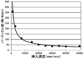
- FIG. 3 shows the relationship between the insertion speed of the silicon wafer into the ozone water tank and the particle measurement results.
- the number of particles on the silicon wafer decreases as the immersion rate in the ozone water bath increases and the insertion rate is 20000 mm / min (Example 1) or more. It was found that the number of particles on the wafer converged and became almost constant. That is, in Examples 1 to 6, the number of particles on the wafer was improved and the quality of the wafer was improved.
- the present invention is not limited to the above embodiment.
- the above-described embodiment is an exemplification, and the present invention has substantially the same configuration as the technical idea described in the claims of the present invention, and any device that exhibits the same function and effect is the present invention. It is included in the technical scope of the invention.
Abstract
The present invention is a method for cleaning a semiconductor wafer in which: a semiconductor wafer is inserted into a hydrofluoric acid tank filled with hydrofluoric acid, immersed in the hydrofluoric acid, and extracted from the hydrofluoric acid tank; and the semiconductor wafer is then inserted into an ozone water tank filled with ozone water, immersed in the ozone water, and cleaned, wherein the method is characterized in that the insertion of the semiconductor wafer into the ozone water tank is performed at an insertion speed of 20,000 mm/min or higher at least from when the lower end of the semiconductor wafer comes into contact with the ozone water to when the semiconductor wafer is completely immersed in the ozone water. There is thereby provided a method for cleaning a semiconductor wafer with which it is possible to prevent particles and other foreign matter from remaining on a semiconductor wafer and to prevent removed foreign matter from re-adhering thereto in a cleaning method in which the semiconductor wafer is cleaned by immersion in hydrofluoric acid and then cleaned by immersion in ozone water.
Description
本発明は、半導体ウェーハの洗浄方法に関する。
The present invention relates to a method for cleaning a semiconductor wafer.
現在、半導体ウェーハのバッチ式洗浄において、フッ酸(HF)とオゾン水を用いた浸漬式の洗浄方法が一般的となっている。この方法では、HF洗浄でウェーハ上の酸化膜を除去するのと同時にパーティクル等の異物を除去し、その後のオゾン水洗浄でウェーハの酸化を行うことによって、自然酸化膜の生成と、残っているパーティクル等の異物の除去を行っている。
Currently, in the batch cleaning of semiconductor wafers, an immersion cleaning method using hydrofluoric acid (HF) and ozone water is common. In this method, a foreign oxide such as particles is removed at the same time as removing the oxide film on the wafer by HF cleaning, and the wafer is oxidized by subsequent ozone water cleaning, thereby generating a natural oxide film and remaining. Foreign matter such as particles is removed.
この時、従来より、半導体ウェーハを洗浄液が充填された洗浄槽内に浸漬(挿入)する速度(浸漬速度)に比べ、洗浄槽から引き上げる(引き出す)速度(引き上げ速度)が重要であるとされている(例えば、特許文献1)。
At this time, the speed at which the semiconductor wafer is pulled up (drawn) (the pulling speed) is more important than the speed at which the semiconductor wafer is immersed (inserted) in the cleaning tank filled with the cleaning liquid (dipping speed). (For example, Patent Document 1).
従来、半導体ウェーハ上に付着するパーティクル等の異物を低減させるために、フッ酸槽からの引き上げ速度を低速とすることが行われている。
Conventionally, in order to reduce foreign matters such as particles adhering to a semiconductor wafer, the pulling rate from the hydrofluoric acid tank is reduced.
半導体ウェーハをフッ酸洗浄して自然酸化膜を剥離すると、ベア面(疎水面)が出ている状態となる。このベア面が出ている状態のウェーハをオゾン水槽にて洗浄(酸化)させる工程において、従来では、オゾン水槽への浸漬(挿入)速度は固定されており、変更することは無く、一般的に10000mm/min程度と低速であった。
When the semiconductor wafer is washed with hydrofluoric acid and the natural oxide film is peeled off, the bare surface (hydrophobic surface) is exposed. In the process of cleaning (oxidizing) the wafer with the bare surface in the ozone water tank, the immersion (insertion) speed into the ozone water tank is conventionally fixed and is not changed. The speed was as low as about 10,000 mm / min.
ところが、オゾン水槽での洗浄工程においては、酸化膜の形成時にパーティクル等の異物の除去も同時に行われるが、浸漬速度が遅い場合、オゾン水と半導体ウェーハの相対速度が遅いために、パーティクルの脱離が起きにくく、パーティクル等の異物が残留してしまう問題があることが判った。
However, in the cleaning process in the ozone water tank, foreign substances such as particles are also removed at the same time as the formation of the oxide film. However, when the immersion speed is slow, the relative speed between the ozone water and the semiconductor wafer is slow, so the particles are removed. It has been found that there is a problem that separation is difficult to occur and foreign matters such as particles remain.
さらに、一般に、オゾン水の薬液の流れが下から上へ流れる向きであるため、洗浄槽の液面付近にパーティクル等の脱離した異物が滞留しやすい。そのため、浸漬速度が遅いと、脱離したパーティクルがウェーハ上の完全に酸化が進んでいない箇所に再付着してしまう問題があることも判ってきた。
Furthermore, generally, since the flow of the chemical solution of ozone water flows from the bottom to the top, foreign substances such as particles are likely to stay near the liquid surface of the cleaning tank. For this reason, it has also been found that when the immersion speed is low, the desorbed particles are reattached to locations on the wafer where oxidation has not progressed completely.
本発明は、上記問題点に鑑みてなされたものであって、半導体ウェーハをフッ酸に浸漬して洗浄した後、オゾン水に浸漬して洗浄する方法において、パーティクル等の異物の残留や除去した異物の再付着を防ぐことができる半導体ウェーハの洗浄方法を提供することを目的とする。
The present invention has been made in view of the above problems, and in the method of cleaning a semiconductor wafer by immersing it in hydrofluoric acid and then immersing it in ozone water, cleaning and removing foreign matters such as particles. It is an object of the present invention to provide a method for cleaning a semiconductor wafer that can prevent reattachment of foreign matters.
上記課題を解決するために、本発明は、半導体ウェーハを、フッ酸を充填したフッ酸槽内に挿入して、前記フッ酸に浸漬し、前記フッ酸槽から引き出した後、前記半導体ウェーハを、オゾン水を充填したオゾン水槽内に挿入して、前記オゾン水に浸漬して洗浄する半導体ウェーハの洗浄方法であって、前記オゾン水槽内への前記半導体ウェーハの挿入を、少なくとも、前記半導体ウェーハの下端が前記オゾン水に接触してから、前記半導体ウェーハが完全にオゾン水に浸漬するまで、挿入速度を20000mm/min以上として行うことを特徴とする半導体ウェーハの洗浄方法を提供する。
In order to solve the above-mentioned problems, the present invention inserts a semiconductor wafer into a hydrofluoric acid tank filled with hydrofluoric acid, immerses it in the hydrofluoric acid, pulls it out from the hydrofluoric acid tank, A method of cleaning a semiconductor wafer that is inserted into an ozone water tank filled with ozone water and is immersed in the ozone water for cleaning, wherein at least the semiconductor wafer is inserted into the ozone water tank The semiconductor wafer cleaning method is characterized in that the insertion speed is set to 20000 mm / min or more until the semiconductor wafer is completely immersed in the ozone water after the lower end of the substrate contacts the ozone water.
このような半導体ウェーハの洗浄方法であれば、パーティクル等の異物の残留や除去した異物の再付着を防ぐことができる。また、搬送速度の高速化にも繋がるため、スループットが向上する。
Such a method for cleaning a semiconductor wafer can prevent foreign matters such as particles from remaining and reattachment of removed foreign matters. In addition, since the transport speed is increased, the throughput is improved.
またこの場合、前記フッ酸槽からの前記半導体ウェーハの引き出しを、引き出し速度1000mm/min以下として行うことが好ましい。
In this case, it is preferable to pull out the semiconductor wafer from the hydrofluoric acid tank at a drawing speed of 1000 mm / min or less.
このようにフッ酸槽からの引き出し速度を低速化させることで、より一層、パーティクル等の異物を低減させることができる。
Thus, by reducing the drawing speed from the hydrofluoric acid tank, foreign matters such as particles can be further reduced.
またこの場合、前記オゾン水槽内への前記半導体ウェーハの挿入を、前記半導体ウェーハの下端が前記オゾン水に接触してから、前記半導体ウェーハの上端が前記オゾン水の液面から50mm以上の位置となるまで、挿入速度を20000mm/min以上として行うことが好ましい。
In this case, the insertion of the semiconductor wafer into the ozone water tank is performed such that the lower end of the semiconductor wafer is in contact with the ozone water, and the upper end of the semiconductor wafer is at a position of 50 mm or more from the liquid level of the ozone water. Until it becomes, it is preferable to perform insertion speed as 20000 mm / min or more.
このようにオゾン水槽内へ半導体ウェーハを挿入することで、オゾン水槽の液面付近に滞留しているパーティクル等の異物の付着を、確実に防止することができるために好ましい。
It is preferable to insert a semiconductor wafer into the ozone water tank in this manner, because it is possible to reliably prevent foreign substances such as particles staying near the liquid surface of the ozone water tank.
また、前記半導体ウェーハとして、シリコンウェーハを洗浄することが好ましい。
Further, it is preferable to clean a silicon wafer as the semiconductor wafer.
本発明の洗浄方法は、シリコンウェーハを洗浄する場合に特に有効である。
The cleaning method of the present invention is particularly effective when cleaning a silicon wafer.
本発明の半導体ウェーハの洗浄方法であれば、半導体ウェーハをフッ酸に浸漬して自然酸化膜を除去した後、オゾン水に浸漬して自然酸化膜を形成する洗浄方法において、パーティクル等の異物の残留や除去した異物の再付着を防ぐことができる。さらに、搬送速度の高速化にも繋がるので、スループットが向上する。
In the method for cleaning a semiconductor wafer according to the present invention, the semiconductor wafer is immersed in hydrofluoric acid to remove the natural oxide film, and then immersed in ozone water to form a natural oxide film. It is possible to prevent reattachment of the remaining or removed foreign matter. Furthermore, it leads to an increase in the conveyance speed, so that the throughput is improved.
上述したように、半導体ウェーハをフッ酸槽に浸漬して自然酸化膜を除去後、オゾン水槽に浸漬することで酸化し、自然酸化膜を形成する方法において、従来の洗浄方法では、パーティクル等の異物が残留する問題や除去した異物が再付着する問題があった。
As described above, after removing a natural oxide film by immersing a semiconductor wafer in a hydrofluoric acid tank, it is oxidized by immersing it in an ozone water tank to form a natural oxide film. There was a problem that foreign matter remained or a removed foreign matter reattached.
そして、本発明者らは上記の問題を解決するために鋭意検討を重ねた結果、オゾン水槽内への半導体ウェーハの挿入を、所定の挿入速度以上とすることによって、パーティクル等の異物の残留や除去した異物の再付着を防ぐことができることを見出し、本発明に到達した。
And, as a result of intensive investigations to solve the above problems, the present inventors have made the insertion of the semiconductor wafer into the ozone water tank at a predetermined insertion speed or higher, so that foreign matters such as particles can remain. The present inventors have found that it is possible to prevent reattachment of the removed foreign matter, and have reached the present invention.
即ち、本発明は、半導体ウェーハを、フッ酸を充填したフッ酸槽内に挿入して、前記フッ酸に浸漬し、前記フッ酸槽から引き出した後、前記半導体ウェーハを、オゾン水を充填したオゾン水槽内に挿入して、前記オゾン水に浸漬して洗浄する半導体ウェーハの洗浄方法であって、前記オゾン水槽内への前記半導体ウェーハの挿入を、少なくとも、前記半導体ウェーハの下端が前記オゾン水に接触してから、前記半導体ウェーハが完全にオゾン水に浸漬するまで、挿入速度を20000mm/min以上として行うことを特徴とする半導体ウェーハの洗浄方法を提供する。
That is, according to the present invention, a semiconductor wafer is inserted into a hydrofluoric acid tank filled with hydrofluoric acid, immersed in the hydrofluoric acid, pulled out from the hydrofluoric acid tank, and then filled with ozone water. A method for cleaning a semiconductor wafer that is inserted into an ozone water tank and immersed in the ozone water for cleaning, wherein the semiconductor wafer is inserted into the ozone water tank so that at least the lower end of the semiconductor wafer is the ozone water. The semiconductor wafer cleaning method is characterized in that the insertion speed is set to 20000 mm / min or more until the semiconductor wafer is completely immersed in ozone water after contacting the substrate.
尚、本発明において「挿入速度」とは、半導体ウェーハと洗浄槽との相対速度をいい、具体的には、(i)半導体ウェーハを引き下げて、所定の位置の洗浄槽に挿入する場合の、半導体ウェーハの引き下げ速度、(ii)洗浄槽を上昇させて所定の位置の半導体ウェーハを洗浄槽に挿入する場合の洗浄槽の上昇速度、(iii)半導体ウェーハの引き下げ及び洗浄槽の上昇が共に行われ、半導体ウェーハの引き下げ速度と洗浄槽の上昇速度を足した速度等のいずれをも含む。以下、「引き出し速度」も同様に、半導体ウェーハと洗浄槽との相対速度をいう。
In the present invention, the “insertion speed” refers to the relative speed between the semiconductor wafer and the cleaning tank. Specifically, (i) when the semiconductor wafer is pulled down and inserted into the cleaning tank at a predetermined position, Both the semiconductor wafer pulling speed, (ii) the cleaning tank rising speed when the cleaning tank is raised and a semiconductor wafer at a predetermined position is inserted into the cleaning tank, and (iii) the semiconductor wafer pulling down and the cleaning tank rise. It includes both of the semiconductor wafer pulling speed and the cleaning tank rising speed. Hereinafter, the “drawing speed” also refers to the relative speed between the semiconductor wafer and the cleaning tank.
以下、本発明の半導体ウェーハの洗浄方法を詳細に説明する。図1に、本発明の半導体ウェーハの洗浄方法の一例を示した洗浄フロー図を示す。
Hereinafter, the semiconductor wafer cleaning method of the present invention will be described in detail. FIG. 1 shows a cleaning flow chart showing an example of a semiconductor wafer cleaning method of the present invention.
本発明において、洗浄対象の半導体ウェーハは、特に限定されないが、シリコンウェーハを用いることができる。
In the present invention, the semiconductor wafer to be cleaned is not particularly limited, but a silicon wafer can be used.
半導体ウェーハに対し、フッ酸洗浄の前に、例えばアンモニア・過酸化水素水洗浄(SC1洗浄)や純水によるリンスを行うことができる(図1(A)、(B))。
The semiconductor wafer can be rinsed with, for example, ammonia / hydrogen peroxide solution cleaning (SC1 cleaning) or pure water before cleaning with hydrofluoric acid (FIGS. 1A and 1B).
次いで、半導体ウェーハを、フッ酸を充填したフッ酸槽内に挿入して、フッ酸に浸漬してフッ酸洗浄を行う(図1(C))。このフッ酸洗浄では、半導体ウェーハに形成されていた自然酸化膜が除去される。フッ酸の濃度や温度は限定されないが、濃度は0.3~3.0%、温度は10~30℃が好ましい。
Next, the semiconductor wafer is inserted into a hydrofluoric acid tank filled with hydrofluoric acid and immersed in hydrofluoric acid to perform hydrofluoric acid cleaning (FIG. 1C). In this hydrofluoric acid cleaning, the natural oxide film formed on the semiconductor wafer is removed. The concentration and temperature of hydrofluoric acid are not limited, but the concentration is preferably 0.3 to 3.0% and the temperature is preferably 10 to 30 ° C.
フッ酸槽からの半導体ウェーハの引き出しは、引き出し速度1000mm/min以下として行うことが好ましい。このように、フッ酸槽からの半導体ウェーハの引き出しを比較的低速で行うことによって、より一層、パーティクル等の異物を低減させることができる。尚、引き出し速度の下限は特に限定されず、0mm/minを超える速度とすることができる。
It is preferable to pull out the semiconductor wafer from the hydrofluoric acid tank at a drawing speed of 1000 mm / min or less. As described above, by removing the semiconductor wafer from the hydrofluoric acid tank at a relatively low speed, foreign matters such as particles can be further reduced. The lower limit of the drawing speed is not particularly limited, and can be a speed exceeding 0 mm / min.
次いで、半導体ウェーハを、オゾン水を充填したオゾン水槽内に挿入して、オゾン水に浸漬して洗浄する(図1(D))。
Next, the semiconductor wafer is inserted into an ozone water tank filled with ozone water and immersed in ozone water for cleaning (FIG. 1D).
図2は、半導体ウェーハをオゾン水槽内に挿入する工程を示す概略図である。本発明は、半導体ウェーハ1を、オゾン水2が充填されたオゾン水槽3内へ挿入するのに際し、少なくとも、半導体ウェーハ1の下端がオゾン水2に接触してから(図2(A))、半導体ウェーハ1が完全にオゾン水2に浸漬する(図2(B))まで、挿入速度を20000mm/min以上として行うことを特徴とする。また、挿入速度の上限は特に限定されないが、通常、50000mm/minが装置限界である。
FIG. 2 is a schematic view showing a process of inserting a semiconductor wafer into an ozone water tank. In the present invention, when the semiconductor wafer 1 is inserted into the ozone water tank 3 filled with the ozone water 2, at least the lower end of the semiconductor wafer 1 comes into contact with the ozone water 2 (FIG. 2A). The insertion speed is 20000 mm / min or more until the semiconductor wafer 1 is completely immersed in the ozone water 2 (FIG. 2B). The upper limit of the insertion speed is not particularly limited, but usually 50000 mm / min is the apparatus limit.
フッ酸槽での洗浄で自然酸化膜が除去された半導体ウェーハ1は、表面がベア面(疎水面)となっているために、非常にパーティクルなどの異物が付着しやすく、また、半導体ウェーハ1に付着している異物の量も多い。
The semiconductor wafer 1 from which the natural oxide film has been removed by washing in a hydrofluoric acid bath has a bare surface (hydrophobic surface), and therefore, foreign substances such as particles are very easily attached to the semiconductor wafer 1. There is also a large amount of foreign matter adhering to the surface.
フッ酸槽での洗浄後のオゾン水槽での洗浄(再酸化処理)において、従来の様に低速(10000mm/min程度)でオゾン水槽内へ浸漬すると、酸化膜形成時にパーティクル等の異物の除去も同時に行われるが、オゾン水と半導体ウェーハの相対速度が遅いために、パーティクルの脱離が起きにくく、パーティクル等の異物が残留してしまう。
In cleaning with ozone water tank after cleaning in hydrofluoric acid tank (re-oxidation treatment), if immersed in ozone water tank at low speed (about 10,000 mm / min) as before, removal of foreign matters such as particles during oxide film formation is also possible. Although it is performed at the same time, since the relative speed between the ozone water and the semiconductor wafer is low, the desorption of particles hardly occurs, and foreign matters such as particles remain.
更に、オゾン水の洗浄液の流れが下から上へ流れる向きであるため、オゾン水槽の液面付近にパーティクル等の脱離した異物が滞留しやすい。そのため、浸漬速度が遅いと脱離したパーティクルがウェーハ上の完全に酸化が進んでいない箇所に再付着してしまう。
Furthermore, since the flow of the cleaning solution of ozone water is from the bottom to the top, foreign substances such as particles are likely to stay near the surface of the ozone water tank. For this reason, when the immersion speed is low, the detached particles are reattached to a location on the wafer where oxidation has not progressed completely.
一方で、本発明のように、半導体ウェーハ1の挿入速度を20000mm/min以上と高速にすると、半導体ウェーハ1からのパーティクルの脱離が効率良くなされ、半導体ウェーハ1をオゾン水槽3内へ素早く沈められるために、液面(槽界面)付近でのパーティクルの再付着が減少し、高品質なウェーハが得られることになる。また、搬送速度の高速化にも繋がるため、スループットが向上する。
On the other hand, when the insertion speed of the semiconductor wafer 1 is increased to 20000 mm / min or more as in the present invention, the desorption of particles from the semiconductor wafer 1 is efficiently performed, and the semiconductor wafer 1 is quickly submerged in the ozone water tank 3. Therefore, the reattachment of particles near the liquid surface (tank interface) is reduced, and a high-quality wafer can be obtained. In addition, since the transport speed is increased, the throughput is improved.
また、本発明では、半導体ウェーハ1の下端がオゾン水2に接触してから(図2(A))、半導体ウェーハ1の上端がオゾン水2の液面から50mm以上の位置となるまで(図2(C))、挿入速度を20000mm/min以上として、半導体ウェーハ1のオゾン水槽3への挿入を行うことが好ましい。このようにすることで、オゾン水槽3の液面付近に滞留しているパーティクル等の異物の付着を、確実に防止することができるために好ましい。またこのとき、図2(C)における半導体ウェーハ1の上端の位置は、オゾン水2の液面から200mm以下とすることができる。
In the present invention, after the lower end of the semiconductor wafer 1 comes into contact with the ozone water 2 (FIG. 2A), the upper end of the semiconductor wafer 1 is at a position of 50 mm or more from the liquid surface of the ozone water 2 (see FIG. 2 (C)), it is preferable to insert the semiconductor wafer 1 into the ozone water tank 3 at an insertion speed of 20000 mm / min or more. By doing in this way, since adhesion of foreign materials, such as the particle | grains which remain | survive near the liquid level of the ozone water tank 3, can be prevented reliably, it is preferable. At this time, the position of the upper end of the semiconductor wafer 1 in FIG. 2C can be set to 200 mm or less from the surface of the ozone water 2.
上記のようにオゾン水槽3内に挿入された半導体ウェーハ1は、ウェーハ保持部4に保持された状態でオゾン水2に浸漬される(図2(D))。オゾン水の濃度は、好ましくは1ppm以上であり、オゾン水の温度は、好ましくは10~30℃であり、好ましい洗浄時間は60~300秒である。
The semiconductor wafer 1 inserted into the ozone water tank 3 as described above is immersed in the ozone water 2 while being held by the wafer holder 4 (FIG. 2 (D)). The concentration of ozone water is preferably 1 ppm or more, the temperature of ozone water is preferably 10 to 30 ° C., and the preferred cleaning time is 60 to 300 seconds.
その後、半導体ウェーハ1をオゾン水槽3から引き出す。この際の引き出し速度については特に限定されず、1000mm/min以下とすることができる。オゾン水による洗浄後は、適宜、乾燥等の処理(図1(E))を行っても良い。
Thereafter, the semiconductor wafer 1 is pulled out from the ozone water tank 3. The drawing speed at this time is not particularly limited, and can be 1000 mm / min or less. After washing with ozone water, treatment such as drying (FIG. 1E) may be performed as appropriate.
尚、オゾン水槽以外のすべての槽において、半導体ウェーハの挿入速度は、高速化することによって悪影響を及ぼすことはなく、パーティクル等の再付着の抑制やスループットの改善が見込まれる。従って、すべての槽の挿入速度を高速とする、例えば、20000mm/min以上とすることが望ましい。
In all the tanks other than the ozone water tank, the insertion speed of the semiconductor wafer is not adversely affected by increasing the speed, and it is expected that the reattachment of particles and the like will be suppressed and the throughput will be improved. Therefore, it is desirable that the insertion speed of all the tanks is high, for example, 20000 mm / min or more.
以下、実施例及び比較例を示して本発明をより具体的に説明するが、本発明はこれらの実施例に限定されるものではない。
Hereinafter, the present invention will be described more specifically with reference to examples and comparative examples, but the present invention is not limited to these examples.
(実施例1~6、比較例1~4)
直径300mmのシリコンウェーハを用いて、アンモニア・過水洗浄→純水リンス→フッ酸洗浄→オゾン水洗浄の順にディップ式洗浄を行い、その後乾燥を行った。その際、オゾン水槽内へのシリコンウェーハの挿入速度を、シリコンウェーハの下端がオゾン水に接触してから、シリコンウェーハの上端がオゾン水の液面から50mmの位置となるまで、表1に示す速度として行った。オゾン水槽以外の槽内への挿入速度は、15000mm/minとし、全ての槽からの引き出し速度は、1000mm/minとした。 (Examples 1 to 6, Comparative Examples 1 to 4)
Using a silicon wafer having a diameter of 300 mm, dip cleaning was performed in the order of ammonia / overwater cleaning → pure water rinsing → hydrofluoric acid cleaning → ozone water cleaning, followed by drying. At that time, the insertion speed of the silicon wafer into the ozone water tank is shown in Table 1 until the lower end of the silicon wafer comes into contact with the ozone water until the upper end of the silicon wafer is positioned 50 mm from the surface of the ozone water. Done as a speed. The insertion speed into tanks other than the ozone water tank was 15000 mm / min, and the drawing speed from all tanks was 1000 mm / min.
乾燥後、KLA-Tencor社製SP5にて、直径16nm以上のパーティクルについて、パーティクル測定を行った。表1に測定されたパーティクル数を示す。図3に、オゾン水槽内へのシリコンウェーハの挿入速度と、パーティクル測定結果との関係を示す。
After drying, particle measurement was performed on particles having a diameter of 16 nm or more using SP5 manufactured by KLA-Tencor. Table 1 shows the number of particles measured. FIG. 3 shows the relationship between the insertion speed of the silicon wafer into the ozone water tank and the particle measurement results.

表1、図3に示されるように、シリコンウェーハ上のパーティクル数は、オゾン水槽への浸漬速度を上昇させていくと共に減少していき、挿入速度が20000mm/min(実施例1)以上であれば、ウェーハ上のパーティクル数は収束していきほぼ一定となることが判った。即ち、実施例1~6では、ウェーハ上のパーティクル数が改善し、ウェーハの品質が向上した。
As shown in Table 1 and FIG. 3, the number of particles on the silicon wafer decreases as the immersion rate in the ozone water bath increases and the insertion rate is 20000 mm / min (Example 1) or more. It was found that the number of particles on the wafer converged and became almost constant. That is, in Examples 1 to 6, the number of particles on the wafer was improved and the quality of the wafer was improved.
一方で、比較例1~比較例4では、パーティクルが多く観察された。
On the other hand, in Comparative Examples 1 to 4, many particles were observed.
なお、本発明は、上記実施形態に限定されるものではない。上記実施形態は、例示であり、本発明の特許請求の範囲に記載された技術的思想と実質的に同一な構成を有し、同様な作用効果を奏するものは、いかなるものであっても本発明の技術的範囲に包含される。
Note that the present invention is not limited to the above embodiment. The above-described embodiment is an exemplification, and the present invention has substantially the same configuration as the technical idea described in the claims of the present invention, and any device that exhibits the same function and effect is the present invention. It is included in the technical scope of the invention.
Claims (4)
- 半導体ウェーハを、フッ酸を充填したフッ酸槽内に挿入して、前記フッ酸に浸漬し、前記フッ酸槽から引き出した後、前記半導体ウェーハを、オゾン水を充填したオゾン水槽内に挿入して、前記オゾン水に浸漬して洗浄する半導体ウェーハの洗浄方法であって、
前記オゾン水槽内への前記半導体ウェーハの挿入を、少なくとも、前記半導体ウェーハの下端が前記オゾン水に接触してから、前記半導体ウェーハが完全にオゾン水に浸漬するまで、挿入速度を20000mm/min以上として行うことを特徴とする半導体ウェーハの洗浄方法。 A semiconductor wafer is inserted into a hydrofluoric acid tank filled with hydrofluoric acid, immersed in the hydrofluoric acid, pulled out from the hydrofluoric acid tank, and then inserted into an ozone water tank filled with ozone water. A method of cleaning a semiconductor wafer that is immersed in the ozone water for cleaning,
Insertion of the semiconductor wafer into the ozone water tank is performed at an insertion speed of 20000 mm / min or more until at least the lower end of the semiconductor wafer is in contact with the ozone water until the semiconductor wafer is completely immersed in the ozone water. A method for cleaning a semiconductor wafer, characterized in that: - 前記フッ酸槽からの前記半導体ウェーハの引き出しを、引き出し速度1000mm/min以下として行うことを特徴とする請求項1に記載の半導体ウェーハの洗浄方法。 2. The method for cleaning a semiconductor wafer according to claim 1, wherein the semiconductor wafer is drawn from the hydrofluoric acid bath at a drawing speed of 1000 mm / min or less.
- 前記オゾン水槽内への前記半導体ウェーハの挿入を、前記半導体ウェーハの下端が前記オゾン水に接触してから、前記半導体ウェーハの上端が前記オゾン水の液面から50mm以上の位置となるまで、挿入速度を20000mm/min以上として行うことを特徴とする請求項1又は請求項2に記載の半導体ウェーハの洗浄方法。 Insertion of the semiconductor wafer into the ozone water tank is performed until the lower end of the semiconductor wafer comes into contact with the ozone water until the upper end of the semiconductor wafer is at a position of 50 mm or more from the surface of the ozone water. The method for cleaning a semiconductor wafer according to claim 1, wherein the cleaning is performed at a speed of 20000 mm / min or more.
- 前記半導体ウェーハとして、シリコンウェーハを洗浄することを特徴とする請求項1から請求項3のいずれか一項に記載の半導体ウェーハの洗浄方法。
The method for cleaning a semiconductor wafer according to any one of claims 1 to 3, wherein a silicon wafer is cleaned as the semiconductor wafer.
Priority Applications (5)
| Application Number | Priority Date | Filing Date | Title |
|---|---|---|---|
| US16/491,294 US11177125B2 (en) | 2017-03-29 | 2018-03-05 | Method for cleaning semiconductor wafer |
| DE112018001115.1T DE112018001115T5 (en) | 2017-03-29 | 2018-03-05 | Method for cleaning a semiconductor wafer |
| KR1020197027585A KR102466269B1 (en) | 2017-03-29 | 2018-03-05 | Semiconductor wafer cleaning method |
| SG11201908278R SG11201908278RA (en) | 2017-03-29 | 2018-03-05 | Method for cleaning semiconductor wafer |
| CN201880019193.1A CN110447088B (en) | 2017-03-29 | 2018-03-05 | Method for cleaning semiconductor wafer |
Applications Claiming Priority (2)
| Application Number | Priority Date | Filing Date | Title |
|---|---|---|---|
| JP2017065628A JP6686955B2 (en) | 2017-03-29 | 2017-03-29 | Semiconductor wafer cleaning method |
| JP2017-065628 | 2017-03-29 |
Publications (1)
| Publication Number | Publication Date |
|---|---|
| WO2018180224A1 true WO2018180224A1 (en) | 2018-10-04 |
Family
ID=63675389
Family Applications (1)
| Application Number | Title | Priority Date | Filing Date |
|---|---|---|---|
| PCT/JP2018/008197 WO2018180224A1 (en) | 2017-03-29 | 2018-03-05 | Method for cleaning semiconductor wafer |
Country Status (8)
| Country | Link |
|---|---|
| US (1) | US11177125B2 (en) |
| JP (1) | JP6686955B2 (en) |
| KR (1) | KR102466269B1 (en) |
| CN (1) | CN110447088B (en) |
| DE (1) | DE112018001115T5 (en) |
| SG (1) | SG11201908278RA (en) |
| TW (1) | TWI755496B (en) |
| WO (1) | WO2018180224A1 (en) |
Families Citing this family (1)
| Publication number | Priority date | Publication date | Assignee | Title |
|---|---|---|---|---|
| JP2021025092A (en) * | 2019-08-06 | 2021-02-22 | 株式会社荏原製作所 | Substrate processing apparatus |
Citations (2)
| Publication number | Priority date | Publication date | Assignee | Title |
|---|---|---|---|---|
| JPH0677201A (en) * | 1992-06-29 | 1994-03-18 | Matsushita Electric Ind Co Ltd | Substrate washing method |
| JP2017011005A (en) * | 2015-06-18 | 2017-01-12 | 信越半導体株式会社 | Method for cleaning silicon wafer |
Family Cites Families (15)
| Publication number | Priority date | Publication date | Assignee | Title |
|---|---|---|---|---|
| JP2839615B2 (en) * | 1990-01-24 | 1998-12-16 | 株式会社東芝 | Cleaning solution for semiconductor substrate and method for manufacturing semiconductor device |
| US5415698A (en) * | 1992-06-29 | 1995-05-16 | Matsushita Electric Industrial Co., Ltd. | Method for cleaning semiconductor wafers |
| JP3146841B2 (en) * | 1994-03-28 | 2001-03-19 | 信越半導体株式会社 | Wafer rinse equipment |
| JP2893676B2 (en) * | 1994-05-19 | 1999-05-24 | 信越半導体株式会社 | HF cleaning method for silicon wafer |
| JP2914555B2 (en) * | 1994-08-30 | 1999-07-05 | 信越半導体株式会社 | Cleaning method for semiconductor silicon wafer |
| JP3202508B2 (en) * | 1994-11-29 | 2001-08-27 | 株式会社東芝 | Semiconductor wafer cleaning method |
| JPH09283483A (en) | 1996-04-08 | 1997-10-31 | Nkk Corp | Equipment and method for washing |
| JPH10256211A (en) * | 1997-03-11 | 1998-09-25 | Sony Corp | Cleaning method for semiconductor substrate |
| US5837662A (en) | 1997-12-12 | 1998-11-17 | Memc Electronic Materials, Inc. | Post-lapping cleaning process for silicon wafers |
| TW426874B (en) * | 1998-10-14 | 2001-03-21 | United Microelectronics Corp | Method for cleaning a semiconductor wafer |
| US6199564B1 (en) * | 1998-11-03 | 2001-03-13 | Tokyo Electron Limited | Substrate processing method and apparatus |
| JP4844912B2 (en) * | 2001-08-01 | 2011-12-28 | 野村マイクロ・サイエンス株式会社 | Photoresist removal method and removal apparatus |
| JP4020810B2 (en) * | 2002-03-29 | 2007-12-12 | 株式会社神戸製鋼所 | Semiconductor carrier lifetime measuring apparatus and method |
| US20050208774A1 (en) * | 2004-01-08 | 2005-09-22 | Akira Fukunaga | Wet processing method and processing apparatus of substrate |
| KR101755826B1 (en) * | 2015-08-13 | 2017-07-10 | 주식회사 엘지실트론 | Wafer cleaning apparatus and Wafer cleaning method |
-
2017
- 2017-03-29 JP JP2017065628A patent/JP6686955B2/en active Active
-
2018
- 2018-03-05 KR KR1020197027585A patent/KR102466269B1/en active IP Right Grant
- 2018-03-05 US US16/491,294 patent/US11177125B2/en active Active
- 2018-03-05 DE DE112018001115.1T patent/DE112018001115T5/en active Pending
- 2018-03-05 SG SG11201908278R patent/SG11201908278RA/en unknown
- 2018-03-05 CN CN201880019193.1A patent/CN110447088B/en active Active
- 2018-03-05 WO PCT/JP2018/008197 patent/WO2018180224A1/en active Application Filing
- 2018-03-09 TW TW107107974A patent/TWI755496B/en active
Patent Citations (2)
| Publication number | Priority date | Publication date | Assignee | Title |
|---|---|---|---|---|
| JPH0677201A (en) * | 1992-06-29 | 1994-03-18 | Matsushita Electric Ind Co Ltd | Substrate washing method |
| JP2017011005A (en) * | 2015-06-18 | 2017-01-12 | 信越半導体株式会社 | Method for cleaning silicon wafer |
Also Published As
| Publication number | Publication date |
|---|---|
| US20200027721A1 (en) | 2020-01-23 |
| SG11201908278RA (en) | 2019-10-30 |
| CN110447088A (en) | 2019-11-12 |
| CN110447088B (en) | 2023-03-28 |
| KR20190129876A (en) | 2019-11-20 |
| US11177125B2 (en) | 2021-11-16 |
| JP6686955B2 (en) | 2020-04-22 |
| DE112018001115T5 (en) | 2019-11-21 |
| TWI755496B (en) | 2022-02-21 |
| KR102466269B1 (en) | 2022-11-11 |
| TW201841244A (en) | 2018-11-16 |
| JP2018170366A (en) | 2018-11-01 |
Similar Documents
| Publication | Publication Date | Title |
|---|---|---|
| KR100846271B1 (en) | Method for cleaning silicon wafer | |
| JP5315596B2 (en) | Manufacturing method of bonded SOI wafer | |
| WO2016203681A1 (en) | Silicon wafer washing method | |
| CN109326501B (en) | Cleaning method for semiconductor wafer after final polishing | |
| WO2018180224A1 (en) | Method for cleaning semiconductor wafer | |
| WO2013179569A1 (en) | Method for cleaning semiconductor wafer | |
| US8288291B2 (en) | Method for removal of bulk metal contamination from III-V semiconductor substrates | |
| JP4817887B2 (en) | Semiconductor substrate cleaning method | |
| JP2009260085A (en) | Method for manufacturing semiconductor device and method for cleaning semiconductor substrate | |
| US11114317B2 (en) | Method for cleaning semiconductor wafer and manufacturing method of semiconductor wafer using the method for cleaning | |
| KR20120092713A (en) | Cleaning method | |
| KR100914606B1 (en) | Method for manufacturing gate oxide film on semiconductor wafer by wet process | |
| JP4357456B2 (en) | Semiconductor substrate cleaning method | |
| JPH0831781A (en) | Washing chemicals | |
| JP4351497B2 (en) | Semiconductor device manufacturing method and semiconductor manufacturing apparatus | |
| JPH0750281A (en) | Cleaning method for silicon wafer | |
| JP4620714B2 (en) | Washing and drying equipment | |
| JP2007266467A (en) | Device and method for manufacturing semiconductor | |
| KR100495653B1 (en) | Process for clearing an wafer | |
| KR100199376B1 (en) | Cleaning apparatus and cleaning method thereby | |
| JP2004140126A (en) | Method of drying semiconductor substrate after cleaning | |
| JP2010123773A (en) | Method of cleaning wafer, and method of manufacturing semiconductor device | |
| JPH0964007A (en) | Cleaning apparatus for semiconductor substrate |
Legal Events
| Date | Code | Title | Description |
|---|---|---|---|
| 121 | Ep: the epo has been informed by wipo that ep was designated in this application |
Ref document number: 18775292 Country of ref document: EP Kind code of ref document: A1 |
|
| ENP | Entry into the national phase |
Ref document number: 20197027585 Country of ref document: KR Kind code of ref document: A |
|
| 122 | Ep: pct application non-entry in european phase |
Ref document number: 18775292 Country of ref document: EP Kind code of ref document: A1 |