WO2018079007A1 - 弾性波装置、高周波フロントエンド回路及び通信装置 - Google Patents
弾性波装置、高周波フロントエンド回路及び通信装置 Download PDFInfo
- Publication number
- WO2018079007A1 WO2018079007A1 PCT/JP2017/028480 JP2017028480W WO2018079007A1 WO 2018079007 A1 WO2018079007 A1 WO 2018079007A1 JP 2017028480 W JP2017028480 W JP 2017028480W WO 2018079007 A1 WO2018079007 A1 WO 2018079007A1
- Authority
- WO
- WIPO (PCT)
- Prior art keywords
- main surface
- bump
- piezoelectric substrate
- substrate
- idt electrode
- Prior art date
- Legal status (The legal status is an assumption and is not a legal conclusion. Google has not performed a legal analysis and makes no representation as to the accuracy of the status listed.)
- Ceased
Links
Images


Classifications
-
- H—ELECTRICITY
- H03—ELECTRONIC CIRCUITRY
- H03F—AMPLIFIERS
- H03F3/00—Amplifiers with only discharge tubes or only semiconductor devices as amplifying elements
- H03F3/20—Power amplifiers, e.g. Class B amplifiers, Class C amplifiers
- H03F3/24—Power amplifiers, e.g. Class B amplifiers, Class C amplifiers of transmitter output stages
-
- H—ELECTRICITY
- H03—ELECTRONIC CIRCUITRY
- H03H—IMPEDANCE NETWORKS, e.g. RESONANT CIRCUITS; RESONATORS
- H03H9/00—Networks comprising electromechanical or electro-acoustic elements; Electromechanical resonators
- H03H9/70—Multiple-port networks for connecting several sources or loads, working on different frequencies or frequency bands, to a common load or source
- H03H9/72—Networks using surface acoustic waves
-
- H—ELECTRICITY
- H03—ELECTRONIC CIRCUITRY
- H03H—IMPEDANCE NETWORKS, e.g. RESONANT CIRCUITS; RESONATORS
- H03H9/00—Networks comprising electromechanical or electro-acoustic elements; Electromechanical resonators
- H03H9/02—Details
- H03H9/02535—Details of surface acoustic wave devices
- H03H9/02818—Means for compensation or elimination of undesirable effects
- H03H9/02834—Means for compensation or elimination of undesirable effects of temperature influence
-
- H—ELECTRICITY
- H03—ELECTRONIC CIRCUITRY
- H03H—IMPEDANCE NETWORKS, e.g. RESONANT CIRCUITS; RESONATORS
- H03H9/00—Networks comprising electromechanical or electro-acoustic elements; Electromechanical resonators
- H03H9/02—Details
- H03H9/05—Holders or supports
- H03H9/0538—Constructional combinations of supports or holders with electromechanical or other electronic elements
- H03H9/0542—Constructional combinations of supports or holders with electromechanical or other electronic elements consisting of a lateral arrangement
-
- H—ELECTRICITY
- H03—ELECTRONIC CIRCUITRY
- H03H—IMPEDANCE NETWORKS, e.g. RESONANT CIRCUITS; RESONATORS
- H03H9/00—Networks comprising electromechanical or electro-acoustic elements; Electromechanical resonators
- H03H9/02—Details
- H03H9/05—Holders or supports
- H03H9/0538—Constructional combinations of supports or holders with electromechanical or other electronic elements
- H03H9/0566—Constructional combinations of supports or holders with electromechanical or other electronic elements for duplexers
- H03H9/0576—Constructional combinations of supports or holders with electromechanical or other electronic elements for duplexers including surface acoustic wave [SAW] devices
-
- H—ELECTRICITY
- H03—ELECTRONIC CIRCUITRY
- H03H—IMPEDANCE NETWORKS, e.g. RESONANT CIRCUITS; RESONATORS
- H03H9/00—Networks comprising electromechanical or electro-acoustic elements; Electromechanical resonators
- H03H9/02—Details
- H03H9/05—Holders or supports
- H03H9/058—Holders or supports for surface acoustic wave devices
- H03H9/059—Holders or supports for surface acoustic wave devices consisting of mounting pads or bumps
-
- H—ELECTRICITY
- H03—ELECTRONIC CIRCUITRY
- H03H—IMPEDANCE NETWORKS, e.g. RESONANT CIRCUITS; RESONATORS
- H03H9/00—Networks comprising electromechanical or electro-acoustic elements; Electromechanical resonators
- H03H9/02—Details
- H03H9/05—Holders or supports
- H03H9/10—Mounting in enclosures
- H03H9/1064—Mounting in enclosures for surface acoustic wave [SAW] devices
-
- H—ELECTRICITY
- H03—ELECTRONIC CIRCUITRY
- H03H—IMPEDANCE NETWORKS, e.g. RESONANT CIRCUITS; RESONATORS
- H03H9/00—Networks comprising electromechanical or electro-acoustic elements; Electromechanical resonators
- H03H9/02—Details
- H03H9/05—Holders or supports
- H03H9/10—Mounting in enclosures
- H03H9/1064—Mounting in enclosures for surface acoustic wave [SAW] devices
- H03H9/1085—Mounting in enclosures for surface acoustic wave [SAW] devices the enclosure being defined by a non-uniform sealing mass covering the non-active sides of the SAW device
-
- H—ELECTRICITY
- H03—ELECTRONIC CIRCUITRY
- H03H—IMPEDANCE NETWORKS, e.g. RESONANT CIRCUITS; RESONATORS
- H03H9/00—Networks comprising electromechanical or electro-acoustic elements; Electromechanical resonators
- H03H9/02—Details
- H03H9/125—Driving means, e.g. electrodes, coils
- H03H9/145—Driving means, e.g. electrodes, coils for networks using surface acoustic waves
-
- H—ELECTRICITY
- H03—ELECTRONIC CIRCUITRY
- H03H—IMPEDANCE NETWORKS, e.g. RESONANT CIRCUITS; RESONATORS
- H03H9/00—Networks comprising electromechanical or electro-acoustic elements; Electromechanical resonators
- H03H9/02—Details
- H03H9/125—Driving means, e.g. electrodes, coils
- H03H9/145—Driving means, e.g. electrodes, coils for networks using surface acoustic waves
- H03H9/14538—Formation
- H03H9/14541—Multilayer finger or busbar electrode
-
- H—ELECTRICITY
- H03—ELECTRONIC CIRCUITRY
- H03H—IMPEDANCE NETWORKS, e.g. RESONANT CIRCUITS; RESONATORS
- H03H9/00—Networks comprising electromechanical or electro-acoustic elements; Electromechanical resonators
- H03H9/25—Constructional features of resonators using surface acoustic waves
-
- H—ELECTRICITY
- H03—ELECTRONIC CIRCUITRY
- H03H—IMPEDANCE NETWORKS, e.g. RESONANT CIRCUITS; RESONATORS
- H03H9/00—Networks comprising electromechanical or electro-acoustic elements; Electromechanical resonators
- H03H9/46—Filters
- H03H9/64—Filters using surface acoustic waves
- H03H9/6489—Compensation of undesirable effects
-
- H—ELECTRICITY
- H03—ELECTRONIC CIRCUITRY
- H03H—IMPEDANCE NETWORKS, e.g. RESONANT CIRCUITS; RESONATORS
- H03H9/00—Networks comprising electromechanical or electro-acoustic elements; Electromechanical resonators
- H03H9/70—Multiple-port networks for connecting several sources or loads, working on different frequencies or frequency bands, to a common load or source
- H03H9/72—Networks using surface acoustic waves
- H03H9/725—Duplexers
-
- H—ELECTRICITY
- H04—ELECTRIC COMMUNICATION TECHNIQUE
- H04B—TRANSMISSION
- H04B1/00—Details of transmission systems, not covered by a single one of groups H04B3/00 - H04B13/00; Details of transmission systems not characterised by the medium used for transmission
- H04B1/38—Transceivers, i.e. devices in which transmitter and receiver form a structural unit and in which at least one part is used for functions of transmitting and receiving
- H04B1/40—Circuits
-
- H—ELECTRICITY
- H03—ELECTRONIC CIRCUITRY
- H03F—AMPLIFIERS
- H03F2200/00—Indexing scheme relating to amplifiers
- H03F2200/451—Indexing scheme relating to amplifiers the amplifier being a radio frequency amplifier
-
- H—ELECTRICITY
- H03—ELECTRONIC CIRCUITRY
- H03F—AMPLIFIERS
- H03F3/00—Amplifiers with only discharge tubes or only semiconductor devices as amplifying elements
- H03F3/20—Power amplifiers, e.g. Class B amplifiers, Class C amplifiers
Definitions
- the present invention relates to an elastic wave device, a high-frequency front end circuit, and a communication device.
- Patent Document 1 discloses an example of an acoustic wave device.
- a transmission filter and a reception filter are mounted on a mounting substrate.
- An insulating material is provided on the mounting substrate so as to cover the transmission filter and the reception filter.
- a piezoelectric layer is provided on a support substrate, and an IDT electrode is provided on the piezoelectric layer.
- the thermal conductivity of the support substrate is higher than the thermal conductivity of the piezoelectric layer.
- An acoustic wave device includes a mounting substrate, a first piezoelectric substrate, a first IDT electrode provided on the first piezoelectric substrate, and a first bump.
- the first piezoelectric substrate has a first main surface which is a main surface on the mounting substrate side, and a second main surface opposite to the first main surface, and the second piezoelectric substrate is , A first main surface which is a main surface on the mounting substrate side, and a second main surface opposite to the first main surface
- the height direction is a direction connecting the mounting substrate and the first piezoelectric substrate, the height of the first bump is H1, and the first bump is bonded to the first piezoelectric substrate.
- An area is A1
- a bonding area of the first bump on the mounting substrate side is B1
- a height of the second bump is H2
- a bonding area of the second bump on the second piezoelectric substrate side is A2.
- the bonding area on the mounting substrate side of the second bump is B2
- the first bump and the second bump are at least one of A1> A2, B1> B2, and H1 ⁇ H2. There is one relationship.
- the first IDT electrode is provided on the first main surface of the first piezoelectric substrate. In this case, heat dissipation can be further enhanced.
- a main surface, the first main surface of the second piezoelectric substrate, and Serial wherein the height direction position of the main surface and the second IDT electrode is positioned within the second main surface is different.
- heat hardly propagates from the first IDT electrode to the second IDT electrode through the sealing resin layer. Therefore, it is less likely that a problem occurs in the reception filter.
- the high-frequency front-end circuit according to the present invention includes an elastic wave device configured according to the present invention and a power amplifier.
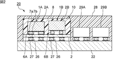
- the first IDT electrode 4A is provided on the first main surface 3Aa of the first piezoelectric substrate 3A.
- a first electrode pad 5A electrically connected to the first IDT electrode 4A is provided on the first main surface 3Aa.
- a first bump 6A is provided on the first electrode pad 5A.
- the first bump 6A is made of, for example, solder.
- the transmission filter 1A is bonded to the mounting substrate 2 by the first bump 6A. More specifically, a plurality of terminals 7a are provided on the main surface of the mounting substrate 2 on the side of the transmission filter 1A and the reception filter 1B. The first electrode pad 5A and the terminal 7a are joined by the first bump 6A. A plurality of terminals 7 b are also provided on the main surface opposite to the main surface of the mounting substrate 2. The first IDT electrode 4A of the transmission filter 1A is electrically connected to the outside through the first electrode pad 5A, the first bump 6A, and the terminals 7a and 7b.
- the reception filter 1B includes a second piezoelectric substrate 3B.
- the second piezoelectric substrate 3B has a first main surface 3Ba that is a surface on the mounting substrate 2 side, and a second main surface 3Bb that faces the first main surface 3Ba.
- the second piezoelectric substrate 3B has a side surface 3Bc that connects the first main surface 3Ba and the second main surface 3Bb.
- the second piezoelectric substrate 3B is not particularly limited, and is made of, for example, a piezoelectric single crystal such as LiTaO 3 or LiNbO 3 or an appropriate piezoelectric ceramic.
- the direction connecting the mounting substrate 2 and the first piezoelectric substrate 3A is the height direction.
- the height of the first bump 6A is H1
- the bonding area of the first bump 6A on the first piezoelectric substrate 3A side is A1
- the bonding area of the first bump 6A on the mounting substrate 2 side is B1.
- the height of the second bump 6B is H2, the bonding area of the second bump 6B on the second piezoelectric substrate 3B side is A2, and the bonding area of the second bump 6B on the mounting substrate 2 side is B2.
- the first bump 6A and the second bump 6B have a relationship of A1> A2, B1> B2, and H1 ⁇ H2.
- the first bump 6A and the second bump 6B may be in a relationship of at least one of A1> A2, B1> B2, and H1 ⁇ H2.
- the height-direction positions of the second main surface 3Ab of the first piezoelectric substrate 3A and the second main surface 3Bb of the second piezoelectric substrate 3B are also different. More specifically, the mounting substrate 2 has a position in the height direction of the second main surface 3Ab of the first piezoelectric substrate 3A that is higher than a position in the height direction of the second main surface 3Bb of the second piezoelectric substrate 3B. Close to.
- the transmission filter generates more heat than the transmission filter and the reception filter.
- the first bump 6A and the second bump 6B have a relationship of A1> A2 and B1> B2.
- the bonding area of the first bump 6A on the first piezoelectric substrate 3A side is large, heat quickly propagates from the first piezoelectric substrate 3A side to the first bump 6A.
- the bonding area of the first bump 6A on the mounting substrate 2 side is large, the heat generated by the heat generation of the transmission filter 1A is quickly propagated to the mounting substrate 2.
- wiring (not shown) that connects the terminals 7a and 7b is provided.
- the first bump 6A and the second bump 6B are preferably in a relationship of A1> A2, B1> B2, and H1 ⁇ H2.
- the first bump 6A and the second bump 6B may be in a relationship of at least one of A1> A2, B1> B2, and H1 ⁇ H2.
- the first piezoelectric substrate 3A side of the first bump 6A and the mounting substrate 2 Large joint area on the side. Thereby, heat quickly propagates from the first piezoelectric substrate 3A side to the mounting substrate 2 side via the first bump 6A.
- the heat radiation path from the transmission filter 1A to the mounting substrate 2 can be shortened.
- the heat generated by the heat generation of the transmission filter 1 ⁇ / b> A quickly propagates to the mounting substrate 2.
- the heat dissipation of the transmission filter 1B can be enhanced via the mounting substrate 2. Therefore, propagation of heat from the transmission filter 1A to the reception filter 1B can be suppressed.
- the second IDT electrode 4B in the reception filter 1B is provided on the first main surface 3Ba of the second piezoelectric substrate 3B.
- heat is generated mainly from the second IDT electrode 4B. Since the second IDT electrode 4B is provided on the first main surface 3Ba, the heat radiation path from the second IDT electrode 4B to the mounting substrate 2 can be shortened. Therefore, the heat dissipation of the reception filter 1B can be effectively improved.
- the first IDT electrode 4A is provided on the second main surface 3Ab of the first piezoelectric substrate 3A, and the second IDT electrode 4B is the second main surface 3Bb of the second piezoelectric substrate 3B. The structure provided above may be sufficient.
- the first IDT electrode 4A and the second IDT electrode 4B are provided on the second main surface 3Ab and the second main surface 3Bb, respectively, the second main surface 3Ab and the second main surface 3Ab It is preferable that the positions in the height direction of the main surface 3Bb are different.
- the acoustic wave device 10 only needs to have at least one pair of transmission filter 1A and reception filter 1B, and other transmission filters and reception filters may be mounted on the mounting substrate 2.
- the elastic wave device 10 of the first embodiment is mounted on the substrate 22. More specifically, the terminal 27 is provided on the substrate 22. The terminal 7 b of the acoustic wave device 10 and the terminal 27 on the substrate 22 are bonded together by a conductive bonding material 26.
- a sealing resin layer 28 is provided on the substrate 22 so as to cover the acoustic wave device 10 and the elements 29A and 29B.
- the heat generated by the heat generation of the transmission filter 1A is radiated to the substrate 22 side via the first bump 6A, the terminals 7a and 7b, the conductive bonding material 26 and the terminal 27.
- the heat dissipation of the elastic wave device 10 can be improved.
- the propagation of heat from the transmission filter 1A to the reception filter 1B can be suppressed.
- the conductive bonding material 26 is preferably a bump. In this case, the heat dissipation of the acoustic wave device 10 can be suitably improved.
- the conductive bonding material 26 is not limited to a bump.
- the high-frequency front-end circuit 230 includes a switch 225, duplexers 201A and 201B, filters 231, 232, low noise amplifier circuits 214, 224, and power amplifier circuits 234a, 234b, 244a, 244b. Note that the high-frequency front-end circuit 230 and the communication device 240 in FIG. 3 are examples of the high-frequency front-end circuit and the communication device, and are not limited to this configuration.
- the filters 231 and 232 in the communication device 240 are connected between the RF signal processing circuit 203 and the switch 225 without passing through the low noise amplifier circuits 214 and 224 and the power amplifier circuits 234a, 234b, 244a and 244b.
- the filters 231 and 232 are also connected to the antenna element 202 via the switch 225, similarly to the duplexers 201A and 201B.
- heat dissipation of heat generated by the heat generated by the transmission filters in the duplexers 201A and 201B is enhanced, and heat is transmitted from the transmission filters to the reception filters. Can be suppressed.
- the elastic wave device, the high-frequency front-end circuit, and the communication device according to the embodiment of the present invention have been described with reference to the embodiment and the modified examples thereof.
- a high-frequency front-end circuit according to the present invention a modification obtained by making various modifications conceived by those skilled in the art without departing from the gist of the present invention, and a high-frequency front-end circuit according to the present invention.
- Various devices incorporating the communication device are also included in the present invention.
- the present invention can be widely used in communication devices such as mobile phones as an elastic wave resonator, a filter, a duplexer, a multiplexer, a front-end circuit, and a communication device applicable to a multiband system.
- SYMBOLS 1A Transmission filter 1B ... Reception filter 2 ... Mounting substrate 3A, 3B ... 1st, 2nd piezoelectric substrate 3Aa, 3Ab ... 1st, 2nd main surface 3Ac ... Side surface 3Ba, 3Bb ... 1st, 2nd main Surface 3Bc: Side surfaces 4A, 4B ... First and second IDT electrodes 5A, 5B ... First and second electrode pads 6A, 6B ... First and second bumps 7a, 7b ... Terminal 8 ... Sealing resin layer DESCRIPTION OF SYMBOLS 10 ... Elastic wave apparatus 20 ... Elastic wave apparatus mounting structure 22 ... Board
Landscapes
- Physics & Mathematics (AREA)
- Acoustics & Sound (AREA)
- Engineering & Computer Science (AREA)
- Power Engineering (AREA)
- Computer Networks & Wireless Communication (AREA)
- Signal Processing (AREA)
- Surface Acoustic Wave Elements And Circuit Networks Thereof (AREA)
Abstract
Description
1B…受信フィルタ
2…実装基板
3A,3B…第1,第2の圧電基板
3Aa,3Ab…第1,第2の主面
3Ac…側面
3Ba,3Bb…第1,第2の主面
3Bc…側面
4A,4B…第1,第2のIDT電極
5A,5B…第1,第2の電極パッド
6A,6B…第1,第2のバンプ
7a,7b…端子
8…封止樹脂層
10…弾性波装置
20…弾性波装置実装構造体
22…基板
26…導電性接合材
27…端子
28…封止樹脂層
29A,29B…素子
201A,201B…デュプレクサ
202…アンテナ素子
203…RF信号処理回路
211,212…フィルタ
214…ローノイズアンプ回路
221,222…フィルタ
224…ローノイズアンプ回路
225…スイッチ
230…高周波フロントエンド回路
231,232…フィルタ
234a,234b…パワーアンプ回路
240…通信装置
244a,244b…パワーアンプ回路
Claims (8)
- 実装基板と、
第1の圧電基板と、前記第1の圧電基板上に設けられている第1のIDT電極と、第1のバンプと、を有し、前記第1のバンプにより前記実装基板に接合されている、送信フィルタと、
第2の圧電基板と、前記第2の圧電基板上に設けられている第2のIDT電極と、第2のバンプと、を有し、前記第2のバンプにより前記実装基板に接合されている、受信フィルタと、
前記送信フィルタ及び前記受信フィルタを覆うように、前記実装基板上に設けられている封止樹脂層と、
を備え、
前記第1の圧電基板が、前記実装基板側の主面である第1の主面と、該第1の主面に対向する第2の主面と、を有し、
前記第2の圧電基板が、前記実装基板側の主面である第1の主面と、該第1の主面に対向する第2の主面と、を有し、
前記実装基板と前記第1の圧電基板とを結ぶ方向を高さ方向とし、前記第1のバンプの高さをH1、前記第1のバンプにおける前記第1の圧電基板側の接合面積をA1、前記第1のバンプにおける前記実装基板側の接合面積をB1とし、前記第2のバンプの高さをH2、前記第2のバンプにおける前記第2の圧電基板側の接合面積をA2、前記第2のバンプにおける前記実装基板側の接合面積をB2としたときに、前記第1のバンプと前記第2のバンプとが、A1>A2かつB1>B2、及びH1<H2のうち少なくとも一方の関係にある、弾性波装置。 - 前記第1のバンプと前記第2のバンプとが、A1>A2かつB1>B2、及びH1<H2の関係にある、請求項1に記載の弾性波装置。
- 前記第1のIDT電極が前記第1の圧電基板の前記第1の主面上に設けられている、請求項1または2に記載の弾性波装置。
- 前記第1の圧電基板における前記第1の主面と前記第2の圧電基板における前記第1の主面との前記高さ方向の位置、及び前記第1の圧電基板における前記第2の主面と前記第2の圧電基板における前記第2の主面との前記高さ方向の位置のうち少なくとも一方が異なる、請求項1~3のいずれか1項に記載の弾性波装置。
- 前記第1のIDT電極及び前記第2のIDT電極の前記第1の圧電基板及び前記第2の圧電基板における配置が、前記第1のIDT電極が前記第1の圧電基板における前記第1の主面上に位置しており、かつ前記第2のIDT電極が前記第2の圧電基板における前記第1の主面上に位置している配置、及び前記第1のIDT電極が前記第1の圧電基板における前記第2の主面上に位置しており、かつ前記第2のIDT電極が前記第2の圧電基板における前記第2の主面上に位置している配置のうち一方の配置であり、
前記第1の圧電基板における前記第1の主面及び前記第2の主面のうち前記第1のIDT電極が位置している主面と、前記第2の圧電基板における前記第1の主面及び前記第2の主面のうち前記第2のIDT電極が位置している主面との前記高さ方向の位置が異なる、請求項4に記載の弾性波装置。 - 前記第2の圧電基板における前記第1の主面の前記高さ方向の位置より、前記第1の圧電基板における前記第1の主面の高さ方向の位置が前記実装基板に近い、請求項4または5に記載の弾性波装置。
- 請求項1~6のいずれか1項に記載の弾性波装置と、
パワーアンプと、
を備える、高周波フロントエンド回路。 - 請求項7に記載の高周波フロントエンド回路と、
RF信号処理回路と、
を備える、通信装置。
Priority Applications (3)
| Application Number | Priority Date | Filing Date | Title |
|---|---|---|---|
| CN201780064154.9A CN109845104B (zh) | 2016-10-28 | 2017-08-04 | 弹性波装置、高频前端电路以及通信装置 |
| KR1020197007163A KR102217746B1 (ko) | 2016-10-28 | 2017-08-04 | 탄성파 장치, 고주파 프론트 엔드 회로 및 통신 장치 |
| US16/375,870 US10637433B2 (en) | 2016-10-28 | 2019-04-05 | Elastic wave device, radio-frequency front-end circuit, and communication device |
Applications Claiming Priority (2)
| Application Number | Priority Date | Filing Date | Title |
|---|---|---|---|
| JP2016-211931 | 2016-10-28 | ||
| JP2016211931 | 2016-10-28 |
Related Child Applications (1)
| Application Number | Title | Priority Date | Filing Date |
|---|---|---|---|
| US16/375,870 Continuation US10637433B2 (en) | 2016-10-28 | 2019-04-05 | Elastic wave device, radio-frequency front-end circuit, and communication device |
Publications (1)
| Publication Number | Publication Date |
|---|---|
| WO2018079007A1 true WO2018079007A1 (ja) | 2018-05-03 |
Family
ID=62023391
Family Applications (1)
| Application Number | Title | Priority Date | Filing Date |
|---|---|---|---|
| PCT/JP2017/028480 Ceased WO2018079007A1 (ja) | 2016-10-28 | 2017-08-04 | 弾性波装置、高周波フロントエンド回路及び通信装置 |
Country Status (4)
| Country | Link |
|---|---|
| US (1) | US10637433B2 (ja) |
| KR (1) | KR102217746B1 (ja) |
| CN (1) | CN109845104B (ja) |
| WO (1) | WO2018079007A1 (ja) |
Families Citing this family (2)
| Publication number | Priority date | Publication date | Assignee | Title |
|---|---|---|---|---|
| JP2022138735A (ja) * | 2021-03-10 | 2022-09-26 | 三安ジャパンテクノロジー株式会社 | 弾性波デバイス、その弾性波デバイスを備えるモジュール、およびその弾性波デバイスの製造方法 |
| CN114094978B (zh) * | 2022-01-19 | 2022-04-15 | 深圳新声半导体有限公司 | 一种声表面滤波器组去耦封装结构 |
Citations (2)
| Publication number | Priority date | Publication date | Assignee | Title |
|---|---|---|---|---|
| JPH1126623A (ja) * | 1997-06-30 | 1999-01-29 | Oki Electric Ind Co Ltd | 電子装置、電子装置の製造方法 |
| JP2015023474A (ja) * | 2013-07-19 | 2015-02-02 | 太陽誘電株式会社 | 分波器 |
Family Cites Families (9)
| Publication number | Priority date | Publication date | Assignee | Title |
|---|---|---|---|---|
| JPH07249657A (ja) | 1994-03-10 | 1995-09-26 | Hitachi Ltd | 半導体集積回路装置 |
| JP2003218150A (ja) * | 2002-01-23 | 2003-07-31 | Fujitsu Media Device Kk | モジュール部品 |
| TW555152U (en) * | 2002-12-13 | 2003-09-21 | Advanced Semiconductor Eng | Structure of flip chip package with area bump |
| WO2009104438A1 (ja) * | 2008-02-18 | 2009-08-27 | 株式会社 村田製作所 | 弾性波装置及びその製造方法 |
| JP2011199810A (ja) * | 2010-03-24 | 2011-10-06 | Murata Mfg Co Ltd | 弾性波分波器 |
| JP5807715B2 (ja) | 2012-03-23 | 2015-11-10 | 株式会社村田製作所 | 弾性波フィルタ素子及びその製造方法 |
| JP6170349B2 (ja) | 2013-06-18 | 2017-07-26 | 太陽誘電株式会社 | 弾性波デバイス |
| KR101754193B1 (ko) * | 2013-08-02 | 2017-07-05 | 가부시키가이샤 무라타 세이사쿠쇼 | 분파장치 |
| WO2015098792A1 (ja) * | 2013-12-25 | 2015-07-02 | 株式会社村田製作所 | 弾性波フィルタデバイス |
-
2017
- 2017-08-04 WO PCT/JP2017/028480 patent/WO2018079007A1/ja not_active Ceased
- 2017-08-04 KR KR1020197007163A patent/KR102217746B1/ko active Active
- 2017-08-04 CN CN201780064154.9A patent/CN109845104B/zh active Active
-
2019
- 2019-04-05 US US16/375,870 patent/US10637433B2/en active Active
Patent Citations (2)
| Publication number | Priority date | Publication date | Assignee | Title |
|---|---|---|---|---|
| JPH1126623A (ja) * | 1997-06-30 | 1999-01-29 | Oki Electric Ind Co Ltd | 電子装置、電子装置の製造方法 |
| JP2015023474A (ja) * | 2013-07-19 | 2015-02-02 | 太陽誘電株式会社 | 分波器 |
Also Published As
| Publication number | Publication date |
|---|---|
| US10637433B2 (en) | 2020-04-28 |
| CN109845104B (zh) | 2022-12-27 |
| KR20190039764A (ko) | 2019-04-15 |
| US20190238112A1 (en) | 2019-08-01 |
| CN109845104A (zh) | 2019-06-04 |
| KR102217746B1 (ko) | 2021-02-19 |
Similar Documents
| Publication | Publication Date | Title |
|---|---|---|
| CN114342073B (zh) | 高频模块以及通信装置 | |
| KR102432608B1 (ko) | 고주파 모듈 및 통신 장치 | |
| KR102431544B1 (ko) | 고주파 모듈 및 통신장치 | |
| CN215646781U (zh) | 高频模块和通信装置 | |
| WO2021006021A1 (ja) | 高周波モジュール及び通信装置 | |
| CN114830543B (zh) | 高频模块以及通信装置 | |
| KR102444727B1 (ko) | 탄성파 장치, 고주파 프론트엔드 회로 및 통신 장치 | |
| CN111418152A (zh) | 弹性波装置、高频前端电路及通信装置 | |
| WO2022009976A1 (ja) | 高周波モジュール及び通信装置 | |
| WO2021124691A1 (ja) | 高周波モジュール及び通信装置 | |
| JP2018078419A (ja) | 弾性波装置、高周波フロントエンド回路及び通信装置 | |
| KR102217746B1 (ko) | 탄성파 장치, 고주파 프론트 엔드 회로 및 통신 장치 | |
| KR20210117949A (ko) | 고주파 모듈 및 통신 장치 | |
| CN114614852B (zh) | 高频模块以及通信装置 | |
| WO2022118891A1 (ja) | 高周波モジュール及び通信装置 | |
| JP2022113172A (ja) | 弾性波デバイス | |
| WO2023047957A1 (ja) | 高周波モジュール、及び、通信装置 | |
| WO2022260015A1 (ja) | 高周波モジュール及び通信装置 | |
| WO2022137708A1 (ja) | 高周波モジュール及び通信装置 | |
| WO2022034823A1 (ja) | 高周波モジュール及び通信装置 | |
| WO2021157177A1 (ja) | 高周波モジュール及び通信装置 | |
| JP2021100213A (ja) | 高周波モジュール及び通信装置 | |
| WO2022145412A1 (ja) | 高周波モジュール及び通信装置 | |
| WO2022014337A1 (ja) | 高周波モジュール及び通信装置 | |
| WO2022209482A1 (ja) | 高周波モジュール及び通信装置 |
Legal Events
| Date | Code | Title | Description |
|---|---|---|---|
| 121 | Ep: the epo has been informed by wipo that ep was designated in this application |
Ref document number: 17866305 Country of ref document: EP Kind code of ref document: A1 |
|
| ENP | Entry into the national phase |
Ref document number: 20197007163 Country of ref document: KR Kind code of ref document: A |
|
| NENP | Non-entry into the national phase |
Ref country code: DE |
|
| 122 | Ep: pct application non-entry in european phase |
Ref document number: 17866305 Country of ref document: EP Kind code of ref document: A1 |
|
| NENP | Non-entry into the national phase |
Ref country code: JP |