WO2018062300A1 - 蒸着マスク、フレーム付き蒸着マスク、蒸着マスク準備体、蒸着パターン形成方法、有機半導体素子の製造方法、有機elディスプレイの製造方法 - Google Patents
蒸着マスク、フレーム付き蒸着マスク、蒸着マスク準備体、蒸着パターン形成方法、有機半導体素子の製造方法、有機elディスプレイの製造方法 Download PDFInfo
- Publication number
- WO2018062300A1 WO2018062300A1 PCT/JP2017/035012 JP2017035012W WO2018062300A1 WO 2018062300 A1 WO2018062300 A1 WO 2018062300A1 JP 2017035012 W JP2017035012 W JP 2017035012W WO 2018062300 A1 WO2018062300 A1 WO 2018062300A1
- Authority
- WO
- WIPO (PCT)
- Prior art keywords
- vapor deposition
- resin
- mask
- deposition mask
- protective sheet
- Prior art date
Links
Images


Classifications
-
- C—CHEMISTRY; METALLURGY
- C23—COATING METALLIC MATERIAL; COATING MATERIAL WITH METALLIC MATERIAL; CHEMICAL SURFACE TREATMENT; DIFFUSION TREATMENT OF METALLIC MATERIAL; COATING BY VACUUM EVAPORATION, BY SPUTTERING, BY ION IMPLANTATION OR BY CHEMICAL VAPOUR DEPOSITION, IN GENERAL; INHIBITING CORROSION OF METALLIC MATERIAL OR INCRUSTATION IN GENERAL
- C23C—COATING METALLIC MATERIAL; COATING MATERIAL WITH METALLIC MATERIAL; SURFACE TREATMENT OF METALLIC MATERIAL BY DIFFUSION INTO THE SURFACE, BY CHEMICAL CONVERSION OR SUBSTITUTION; COATING BY VACUUM EVAPORATION, BY SPUTTERING, BY ION IMPLANTATION OR BY CHEMICAL VAPOUR DEPOSITION, IN GENERAL
- C23C14/00—Coating by vacuum evaporation, by sputtering or by ion implantation of the coating forming material
- C23C14/22—Coating by vacuum evaporation, by sputtering or by ion implantation of the coating forming material characterised by the process of coating
- C23C14/24—Vacuum evaporation
-
- C—CHEMISTRY; METALLURGY
- C23—COATING METALLIC MATERIAL; COATING MATERIAL WITH METALLIC MATERIAL; CHEMICAL SURFACE TREATMENT; DIFFUSION TREATMENT OF METALLIC MATERIAL; COATING BY VACUUM EVAPORATION, BY SPUTTERING, BY ION IMPLANTATION OR BY CHEMICAL VAPOUR DEPOSITION, IN GENERAL; INHIBITING CORROSION OF METALLIC MATERIAL OR INCRUSTATION IN GENERAL
- C23C—COATING METALLIC MATERIAL; COATING MATERIAL WITH METALLIC MATERIAL; SURFACE TREATMENT OF METALLIC MATERIAL BY DIFFUSION INTO THE SURFACE, BY CHEMICAL CONVERSION OR SUBSTITUTION; COATING BY VACUUM EVAPORATION, BY SPUTTERING, BY ION IMPLANTATION OR BY CHEMICAL VAPOUR DEPOSITION, IN GENERAL
- C23C14/00—Coating by vacuum evaporation, by sputtering or by ion implantation of the coating forming material
- C23C14/04—Coating on selected surface areas, e.g. using masks
- C23C14/042—Coating on selected surface areas, e.g. using masks using masks
-
- C—CHEMISTRY; METALLURGY
- C23—COATING METALLIC MATERIAL; COATING MATERIAL WITH METALLIC MATERIAL; CHEMICAL SURFACE TREATMENT; DIFFUSION TREATMENT OF METALLIC MATERIAL; COATING BY VACUUM EVAPORATION, BY SPUTTERING, BY ION IMPLANTATION OR BY CHEMICAL VAPOUR DEPOSITION, IN GENERAL; INHIBITING CORROSION OF METALLIC MATERIAL OR INCRUSTATION IN GENERAL
- C23C—COATING METALLIC MATERIAL; COATING MATERIAL WITH METALLIC MATERIAL; SURFACE TREATMENT OF METALLIC MATERIAL BY DIFFUSION INTO THE SURFACE, BY CHEMICAL CONVERSION OR SUBSTITUTION; COATING BY VACUUM EVAPORATION, BY SPUTTERING, BY ION IMPLANTATION OR BY CHEMICAL VAPOUR DEPOSITION, IN GENERAL
- C23C16/00—Chemical coating by decomposition of gaseous compounds, without leaving reaction products of surface material in the coating, i.e. chemical vapour deposition [CVD] processes
- C23C16/04—Coating on selected surface areas, e.g. using masks
- C23C16/042—Coating on selected surface areas, e.g. using masks using masks
-
- C—CHEMISTRY; METALLURGY
- C23—COATING METALLIC MATERIAL; COATING MATERIAL WITH METALLIC MATERIAL; CHEMICAL SURFACE TREATMENT; DIFFUSION TREATMENT OF METALLIC MATERIAL; COATING BY VACUUM EVAPORATION, BY SPUTTERING, BY ION IMPLANTATION OR BY CHEMICAL VAPOUR DEPOSITION, IN GENERAL; INHIBITING CORROSION OF METALLIC MATERIAL OR INCRUSTATION IN GENERAL
- C23C—COATING METALLIC MATERIAL; COATING MATERIAL WITH METALLIC MATERIAL; SURFACE TREATMENT OF METALLIC MATERIAL BY DIFFUSION INTO THE SURFACE, BY CHEMICAL CONVERSION OR SUBSTITUTION; COATING BY VACUUM EVAPORATION, BY SPUTTERING, BY ION IMPLANTATION OR BY CHEMICAL VAPOUR DEPOSITION, IN GENERAL
- C23C16/00—Chemical coating by decomposition of gaseous compounds, without leaving reaction products of surface material in the coating, i.e. chemical vapour deposition [CVD] processes
- C23C16/44—Chemical coating by decomposition of gaseous compounds, without leaving reaction products of surface material in the coating, i.e. chemical vapour deposition [CVD] processes characterised by the method of coating
-
- H—ELECTRICITY
- H10—SEMICONDUCTOR DEVICES; ELECTRIC SOLID-STATE DEVICES NOT OTHERWISE PROVIDED FOR
- H10K—ORGANIC ELECTRIC SOLID-STATE DEVICES
- H10K50/00—Organic light-emitting devices
- H10K50/10—OLEDs or polymer light-emitting diodes [PLED]
- H10K50/11—OLEDs or polymer light-emitting diodes [PLED] characterised by the electroluminescent [EL] layers
-
- H—ELECTRICITY
- H10—SEMICONDUCTOR DEVICES; ELECTRIC SOLID-STATE DEVICES NOT OTHERWISE PROVIDED FOR
- H10K—ORGANIC ELECTRIC SOLID-STATE DEVICES
- H10K59/00—Integrated devices, or assemblies of multiple devices, comprising at least one organic light-emitting element covered by group H10K50/00
- H10K59/10—OLED displays
- H10K59/12—Active-matrix OLED [AMOLED] displays
-
- H—ELECTRICITY
- H10—SEMICONDUCTOR DEVICES; ELECTRIC SOLID-STATE DEVICES NOT OTHERWISE PROVIDED FOR
- H10K—ORGANIC ELECTRIC SOLID-STATE DEVICES
- H10K71/00—Manufacture or treatment specially adapted for the organic devices covered by this subclass
-
- H—ELECTRICITY
- H10—SEMICONDUCTOR DEVICES; ELECTRIC SOLID-STATE DEVICES NOT OTHERWISE PROVIDED FOR
- H10K—ORGANIC ELECTRIC SOLID-STATE DEVICES
- H10K71/00—Manufacture or treatment specially adapted for the organic devices covered by this subclass
- H10K71/10—Deposition of organic active material
- H10K71/16—Deposition of organic active material using physical vapour deposition [PVD], e.g. vacuum deposition or sputtering
- H10K71/164—Deposition of organic active material using physical vapour deposition [PVD], e.g. vacuum deposition or sputtering using vacuum deposition
-
- H—ELECTRICITY
- H10—SEMICONDUCTOR DEVICES; ELECTRIC SOLID-STATE DEVICES NOT OTHERWISE PROVIDED FOR
- H10K—ORGANIC ELECTRIC SOLID-STATE DEVICES
- H10K71/00—Manufacture or treatment specially adapted for the organic devices covered by this subclass
- H10K71/10—Deposition of organic active material
- H10K71/16—Deposition of organic active material using physical vapour deposition [PVD], e.g. vacuum deposition or sputtering
- H10K71/166—Deposition of organic active material using physical vapour deposition [PVD], e.g. vacuum deposition or sputtering using selective deposition, e.g. using a mask
Definitions
- Embodiments of the present disclosure relate to a vapor deposition mask, a vapor deposition mask with a frame, a vapor deposition mask preparation, a vapor deposition pattern forming method, a method for manufacturing an organic semiconductor element, and a method for manufacturing an organic EL display.
- Formation of a vapor deposition pattern using a vapor deposition mask is usually performed by bringing a vapor deposition mask provided with an opening corresponding to a pattern to be vapor-deposited and an object to be vapor-deposited, and allowing a vapor deposition material released from a vapor deposition source to pass through the opening. It is performed by adhering to a vapor deposition object. Moreover, the said vapor deposition mask is fixed to a flame
- a metal mask having a resin mask opening having a resin mask opening corresponding to the pattern to be vapor deposited and a metal mask opening (sometimes referred to as a slit).
- a vapor deposition mask (for example, Patent Documents 1 to 5) is known.
- Japanese Patent No. 5288072 Japanese Patent No. 5288073 Japanese Patent No. 5288074 JP 2014-218735 A Japanese Patent No. 6163376
- the main object of the embodiment of the present disclosure is to provide a vapor deposition mask capable of forming a high-definition vapor deposition pattern.
- a vapor deposition mask includes a resin mask having a resin mask opening corresponding to a pattern to be vapor-deposited, and a metal layer partially positioned on one surface of the resin mask.
- the resin mask may have a quadrilateral shape having a long side and a short side, and the metal layer may have a band shape along the long side of the resin mask.
- a vapor deposition mask with a frame according to another embodiment of the present disclosure includes the vapor deposition mask according to the embodiment of the present disclosure and a frame, and the vapor deposition mask is fixed to the frame via the metal layer.
- a vapor deposition mask with a frame according to another embodiment of the present disclosure includes the vapor deposition mask according to the embodiment of the present disclosure and a frame, and the vapor deposition mask is fixed to the frame via the resin mask.
- a deposition mask with a frame according to another embodiment of the present disclosure includes the deposition mask according to the embodiment of the present disclosure and a frame, and the deposition mask is interposed through both the resin mask and the metal layer. Fixed to the frame.
- a vapor deposition mask preparation according to another embodiment of the present disclosure is a vapor deposition mask preparation for manufacturing the vapor deposition mask according to the embodiment of the present disclosure, and includes a resin plate and one surface of the resin plate. A metal layer partially located thereon.
- the vapor deposition mask used is the vapor deposition mask according to the embodiment of the present disclosure.
- the manufacturing method of the organic-semiconductor element concerning another one Embodiment of this indication includes the vapor deposition pattern formation process which forms a vapor deposition pattern in a vapor deposition target object using a vapor deposition mask,
- the vapor deposition mask is a vapor deposition mask according to the embodiment of the present disclosure.
- an organic EL element manufactured by the method for manufacturing an organic semiconductor element according to the embodiment of the present disclosure is used for the method of manufacturing the organic EL display according to another embodiment of the present disclosure.
- a high-definition vapor deposition pattern can be formed.
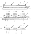
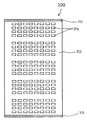
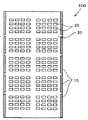
- (A) is a front view which shows an example when the vapor deposition mask concerning embodiment of this indication is planarly viewed from the side in which the metal layer is formed
- (b) is AA part of (a) It is a schematic sectional drawing in. It is a front view which shows an example when the vapor deposition mask concerning another embodiment of this indication is planarly viewed from the side in which the metal layer is formed. It is a front view which shows an example when the vapor deposition mask concerning another embodiment of this indication is planarly viewed from the side in which the metal layer is formed.
- FIG. It is a figure which shows an example of the device which has an organic EL display. It is process drawing which shows an example of the manufacturing method of a vapor deposition mask. It is process drawing which shows an example of the manufacturing method of a vapor deposition mask preparation body.
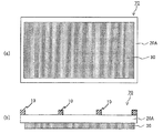
- (A) is a front view when the vapor deposition mask preparation body as an example is planarly viewed from the protection sheet side,
- (b) is a schematic sectional drawing of the vapor deposition mask preparation body of (a).
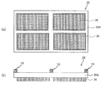
- (A) is a front view when the vapor deposition mask preparation body as an example is planarly viewed from the protection sheet side
- (b) is a schematic sectional drawing of the vapor deposition mask preparation body of (a).
- (A)-(c) is a front view when the vapor deposition mask preparation as an example is planarly viewed from the protective sheet side. It is a front view which shows an example when the vapor deposition mask concerning another embodiment of this indication is planarly viewed from the side in which the metal layer is formed. It is a front view which shows an example when the vapor deposition mask concerning another embodiment of this indication is planarly viewed from the side in which the metal layer is formed.
- FIG.1 (a) is a front view which shows an example when the vapor deposition mask concerning embodiment of this indication is planarly viewed from the side in which the metal layer is formed
- FIG.1 (b) is FIG.1 (a). Is a schematic cross-sectional view taken along the line AA of FIG. Note that a portion near the center of the vapor deposition mask in FIG. 1B is omitted.
- a deposition mask 100 includes a resin mask 20 having a resin mask opening 25 corresponding to a pattern to be deposited, and the resin mask 20. 1 side, the metal layer 10 partially located on the upper surface in FIG.1 (b) is included.
- the weight can be reduced as compared with a vapor deposition mask using a conventional metal.
- the resin mask opening 25 can be further refined. You can also.
- the metal layer 10 is partially provided on one surface of the resin mask 20 as described above, the resin mask 20 can be prevented from being bent and handling can be simplified.
- the vapor deposition mask 100 is often used while being fixed to a metal frame. However, since the metal layer 10 is provided, the metal layer 10 and the frame are fixed to the frame.
- the vapor deposition mask 100 can be fixed to the frame simply and accurately. Furthermore, according to such a vapor deposition mask 100, since the metal layer 10 is provided, the stiffness of the resin mask 20 can be strengthened, so that the vapor deposition mask is wrinkled when fixed to the frame. Can be suppressed.
- the vapor deposition mask is usually fixed to the frame in a state where a tensile member (for example, a clamp) is fixed to the end of the vapor deposition mask and the tensile member is pulled outward of the vapor deposition mask.
- the resin mask 20 constituting the vapor deposition mask 100 according to the embodiment of the present disclosure is not particularly limited, and can be appropriately selected from conventionally known various resin masks 20.
- a high-definition resin mask opening 25 can be formed by laser processing or the like, and it is preferable to use a light material that has a small dimensional change rate and moisture absorption rate over time and with time.
- Such materials include polyimide resin, polyamide resin, polyamideimide resin, polyester resin, polyethylene resin, polyvinyl alcohol resin, polypropylene resin, polycarbonate resin, polystyrene resin, polyacrylonitrile resin, ethylene vinyl acetate copolymer resin, ethylene- Examples thereof include vinyl alcohol copolymer resin, ethylene-methacrylic acid copolymer resin, polyvinyl chloride resin, polyvinylidene chloride resin, cellophane, and ionomer resin.
- a resin material having a moisture absorption rate of 1.0% or less is preferable, and a resin material having both conditions is particularly preferable.
- the thickness of the resin mask 20 is not particularly limited, but in the case of further improving the effect of suppressing the generation of shadows, the thickness of the resin mask 20 is preferably 25 ⁇ m or less, and more preferably less than 10 ⁇ m. .
- the preferable range of the lower limit value when the thickness of the resin mask 20 is less than 3 ⁇ m, defects such as pinholes are likely to occur, and the risk of deformation and the like increases.
- the thickness of the resin mask 20 by setting the thickness of the resin mask 20 to 3 ⁇ m or more and less than 10 ⁇ m, more preferably 4 ⁇ m or more and 8 ⁇ m or less, it is possible to more effectively prevent the influence of shadows when forming a high-definition pattern exceeding 400 ppi. .
- the resin mask 20 and the metal layer 10 to be described later may be joined directly or via an adhesive layer, but the resin mask 20 and the metal layer via the adhesive layer. 10 is bonded, it is preferable that the total thickness of the resin mask 20 and the pressure-sensitive adhesive layer is within the range of the preferable thickness.
- a shadow is a film that is thinner than the target deposition thickness because part of the deposition material released from the deposition source does not reach the deposition target by colliding with the inner wall surface of the opening of the resin mask. This refers to a phenomenon in which an undeposited portion that becomes thick occurs.
- the cross-sectional shape of the resin mask opening 25 is not particularly limited, and the end faces of the resin mask that form the resin mask opening 25 may be substantially parallel to each other. However, as shown in FIG. It is preferable that the cross-sectional shape of the mask opening 25 is a shape that expands toward the vapor deposition source. In other words, it preferably has a gradient (sometimes referred to as a taper) that expands toward the surface on which the metal layer is formed.
- the angle of the gradient can be appropriately set in consideration of the thickness of the resin mask 20, etc., and a straight line connecting the lower bottom tip in the resin mask opening 25 and the upper bottom tip in the resin mask opening,
- the angle formed with the bottom surface of the resin mask in other words, the surface on the side that does not contact the inner wall surface of the resin mask opening 25 and the metal layer 10 of the resin mask 20 in the cross section in the thickness direction of the inner wall surface constituting the resin mask opening 25.
- the angle formed with the lower surface of the resin mask is preferably in the range of 5 ° to 85 °, more preferably in the range of 15 ° to 75 °, and 25 °. More preferably, it is in the range of 65 ° or less.
- the end face forming the resin mask opening 25 has a linear shape, but is not limited to this, and has an outwardly convex curved shape, that is, the resin mask opening.
- the entire shape of 25 may be a bowl shape. Further, it may be the opposite, that is, it may have a convex curved shape.
- “one screen” including an aggregate of a plurality of resin mask openings 25 is formed on the resin mask 20 constituting the vapor deposition mask at a predetermined interval. Multiple screens are arranged with a gap.
- the resin mask opening 25 referred to here means a pattern to be produced using the vapor deposition mask 100 according to the embodiment of the present disclosure.
- the vapor deposition mask is formed as an organic layer in an organic EL display.
- the shape of the resin mask opening 25 is the shape of the organic layer.
- “one screen” consists of an assembly of resin mask openings 25 corresponding to one product. When the one product is an organic EL display, one organic EL display is formed.
- An aggregate of necessary organic layers, that is, an aggregate of resin mask openings 25 serving as an organic layer is “one screen”.
- Metal layer As shown in FIG. 1, in the vapor deposition mask 100 according to the embodiment of the present disclosure, a metal layer 10 is partially provided on one surface of the resin mask 20.
- the material of the metal layer 10 constituting the vapor deposition mask 100 according to the embodiment of the present disclosure is not particularly limited, and examples thereof include metal materials such as stainless steel, iron-nickel alloy, and aluminum alloy. Further, other metal materials may be used. Among them, an invar material that is an iron-nickel alloy can be suitably used because it is less deformed by heat.
- the thickness of the metal layer 10 is not particularly limited, but is preferably 100 ⁇ m or less, more preferably 50 ⁇ m or less, and more preferably 35 ⁇ m or less in order to more effectively prevent the occurrence of shadows. Particularly preferred. When the thickness is less than 5 ⁇ m, the risk of breakage and deformation increases and handling tends to be difficult.
- the several metal layer 10 is arrange
- the cross-sectional shape of the metal layer 10 is not particularly limited, and as shown in FIG. 1B, the end faces facing each other of the metal layer 10 may be substantially parallel to each other. Similarly to the resin mask opening 25, it may have a gradient shape.
- the position where the metal layer 10 is provided and the shape of the metal layer when viewed in plan are not particularly limited. That is, the planar shape of the metal layer can be appropriately designed according to the position where the metal layer is provided.
- the resin mask 20 constituting the vapor deposition mask 100 when the resin mask 20 constituting the vapor deposition mask 100 is viewed in plan, the resin mask 20 exhibits a quadrangle having a long side and a short side, for example, a rectangle.
- the metal layer may have a band shape along the long side of the resin mask.
- the metal layer 10 may be disposed in parallel with the short side of the resin mask 20 while forming a strip shape having the same length as the short side.
- the metal mask 10 is formed when the resin mask 20 exhibits a rectangle having a long side and a short side.
- the shape of the metal layer may be a band shape having a predetermined angle with respect to the long side of the resin mask.
- the quadrilateral is not limited to a rectangle, and may be a trapezoid or a parallelogram, for example. Other quadrilaterals may be used.
- the shape and arrangement of the metal layer 10 described in the present specification can be applied as appropriate to the resin mask 20 having a shape other than the quadrangular shape when the resin mask 20 is planarized.
- each band-shaped metal layers 10 are arranged in parallel with the short sides of the resin mask 20, and in the form shown in FIG. 14, three bands in parallel with the long sides of the resin mask 20.
- the shape metal layer 10 is arranged, the number of the metal layers 10 arranged is not limited. For example, although not illustrated, only one metal layer 10 of the plurality of metal layers 10 is arranged. It is good also as the form which arrange
- a band-shaped metal layer 10 having the same length as the short side may be disposed only in the vicinity of the upper side and the lower side of the resin mask 20, and as shown in FIG.
- the band-shaped metal layer 10 having the same length as the long side may be disposed only on the left side of the mask 20 and in the vicinity of the right side. Moreover, it is good also as a strip
- the metal layer 10 located near the upper and lower sides of the resin mask, or near the right and left sides of the resin mask is disposed so as to be in contact with the circumference of the resin mask 20. However, it may not be in contact with the periphery.
- the metal layer 10 may be disposed only on the peripheral edge of the resin mask 20.
- the peripheral part of the resin mask 20 as used in this specification means the area
- the metal layer 10 may be arranged only in the vicinity of one or both of the upper side and the lower side of the resin mask in the peripheral part of the resin mask 20. In this case, the metal layer 10 may be disposed so as to contact the periphery of the resin mask.
- a metal layer having a length different from the long side or the short side of the resin mask 20 is used instead of the strip-shaped metal layer 10 having the same length as the long side or the short side of the resin mask 20 .
- One may be arranged in parallel with 20 long sides or short sides, or a plurality of them may be arranged.
- One or a plurality of band-shaped metal layers 10 may be arranged in random directions.
- the strip-shaped metal layer 10 having a length shorter than the right side and the left side, that is, the long side of the resin mask 20 is arranged at positions separated from the peripheral edges of the right side and the left side of the resin mask 20. May be.
- the region where the metal layer 10 is disposed in FIG. 16 may be a peripheral portion of the resin mask 20 or a non-peripheral portion.
- region which straddles a peripheral part and a non-peripheral part may be sufficient.
- the non-peripheral part of the resin mask 20 as used in this specification means the whole area
- the strip-shaped metal layer 10 arranged in parallel to the long side of the resin mask 20 is divided into a plurality of pieces in the length direction and five pieces in FIG. Also good.
- the metal layer 10 is preferably arranged in parallel to the long side having a large amount of change such as elongation or shrinkage.
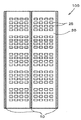
- FIG. 2 is a front view showing an example when a vapor deposition mask according to another embodiment of the present disclosure is viewed in plan view from the side on which the metal layer is formed.
- the metal layer 10 is not necessarily required to be positioned on the peripheral edge of the resin mask 20.
- FIG. 2 shows an example in which the metal layer 10 is positioned only on the non-peripheral portion of the resin mask 20. Further, the metal layer 10 may be disposed on the peripheral edge and the non-peripheral edge of the resin mask 20.
- the metal layer 10 is used only for fixing to the frame by disposing the metal layer 10 on the non-peripheral portion of the resin mask 20, specifically, at a position that does not overlap the frame in the resin mask 20. Instead, deformation such as elongation or shrinkage that can occur in the resin mask 20 can be effectively suppressed.
- the resin mask 20 is fixed when the vapor deposition mask is fixed to the frame as compared with the case where the metal layer surrounds the periphery of the opening 25 formed in the resin mask 20. It is possible to appropriately release the stress that can be generated in the film, and as a result, it is possible to effectively suppress deformation such as expansion and contraction.
- the dotted line shown in FIG. 2 indicates the “one screen” area.
- the metal layer 10 may be disposed between “one screen” and “one screen”.
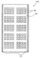
- FIG. 3 is a front view showing an example when a vapor deposition mask according to still another embodiment of the present disclosure is viewed in plan view from the side on which the metal layer is formed.
- the metal layer 10 does not necessarily have a strip shape, and may be arranged so as to be scattered on the resin mask 20. Further, as shown in FIG. It may be arranged only at the four corners of the resin mask 20. In such a case, the metal layer 10 shown in FIG. 3 and FIG. 18 is a square, but is not limited to this, and is not limited to this, but a rectangle, a triangle, a quadrilateral or more, a circle, an ellipse, a semicircle, a donut. Any shape such as a shape, an alphabetic “C” shape, a “T” shape, a “cross” shape or a “star” shape can be employed.
- the vapor deposition mask 100 does not need to be configured only by the resin mask 20 and the metal layer 10 as illustrated in FIGS. 1 to 3, 11, and 14 to 18.
- a protective sheet may be a protective film, a protective layer, or a protective plate
- the resin mask opening 25 is formed by laser processing, the generation of burrs and debris can be suppressed, and the resin mask opening 25 is formed during laser processing. It is possible to prevent the peripheral strength from being lowered.
- the manufacturing method of such a vapor deposition mask 100 is not particularly limited. For example, by preparing a resin plate and forming a metal layer at a desired position on the resin plate, a resin plate with a metal layer, a so-called vapor deposition mask preparation is formed.
- the method for forming the metal layer in this case is not particularly limited, and the metal layer can be formed by various plating methods, etching methods, various printing methods, vapor deposition methods, and the like.
- the vapor deposition mask 100 can be obtained by forming an opening having a desired shape in the resin plate in the state of the resin plate with the metal layer or after being fixed to the frame 60 by laser processing or the like.
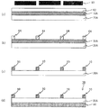
- the manufacturing method of the vapor deposition mask includes the resin mask 20 having the resin mask opening 25 corresponding to the pattern to be vapor-deposited, and the metal layer 10 partially located on one surface of the resin mask 20. As shown in FIG. 6A, the metal layer 10 is partially located on one surface of the resin plate 20A for obtaining the resin mask 20, as shown in FIG.
- FIG. 6 is a process diagram illustrating an example of a method for manufacturing a vapor deposition mask according to an embodiment of the present disclosure.
- the peel strength referred to in this specification is synonymous with 180 ° peeling adhesive strength based on JIS Z-0237: 2009, and the measurement of peel strength is (Method 2) in JIS Z-0237: 2009: back side It can be performed in accordance with the peel strength of 180 °.
- a test tape a polyimide film having an adhesive on its surface (polyimide tape 5413 (manufactured by 3M Japan)) is bonded to a stainless steel plate so that the stainless steel plate and the adhesive face each other.
- a test sheet is used, a protective sheet as a test piece is attached to the polyimide film of this test board, and the peel strength when the protective sheet as a test piece is peeled 180 ° from the polyimide film as a test board (against polyimide) Can be measured by a method according to JIS Z-0237: 2009, and the peel strength of the protective sheet can be measured.
- the measuring device for measuring the peel strength is an electromechanical universal testing machine (5900 series instrument). Ron).
- the vapor deposition mask manufacturing method using the vapor deposition mask preparation 70 when the resin plate 20A of the vapor deposition mask preparation 70 is irradiated with laser light and the resin plate 20A is disassembled to form the resin mask opening 25.
- the vapor deposition mask 100 which can form a high-definition vapor deposition pattern can be obtained.
- the protective sheet 30 provided on the other surface of the resin plate 20A can suppress focus blurring when the resin plate 20A is irradiated with laser light to form the resin mask opening 25.
- the occurrence of “burrs” and “wrinkles” due to insufficient disassembly of the resin plate 20A due to the focus blur can be suppressed.
- the vapor deposition mask preparation 70 for example, when the vapor deposition mask preparation 70 is placed on the processing stage 75 to form the resin mask opening 25, the processing stage 75 and the vapor deposition mask preparation 70 Even when a gap is generated between them, it is possible to suppress focus blurring when the resin mask 20A is formed by irradiating the resin plate 20A with laser light.
- the strength of the resin plate 20A itself can be increased. This also makes it possible to suppress the occurrence of “burrs” and “wrinkles”.
- the presence of the protective sheet 30 provided on the other surface of the resin plate 20A prevents the recesses that will eventually become the resin mask opening 25 and the strength reduction of the resin plate 20A in the vicinity of the recesses. Can be planned.
- the protective sheet 30 is a resin plate, the apparent thickness of the resin plate 20A can be increased.
- the protective sheet 30 serves as a support for preventing the focus blur and for preventing the strength of the resin plate from being lowered.
- the protective sheet 30 provided on the other surface of the resin plate 20A prevents laser light from decreasing in strength of the recess that will eventually become the resin mask opening 25 and the resin plate 20A in the vicinity of the recess.
- the resin mask opening is formed in the resin plate 20A by irradiation, it is possible to prevent the resin plate 20A from being partially cut off.
- the manufacturing method of the vapor deposition mask according to the embodiment of the present disclosure it is possible to suppress the occurrence of “burrs” and “wrinkles” when the resin mask opening 25 is formed in the resin plate 20A.
- the resin mask opening 25 can be accurately formed in the plate 20A.
- resin board 20A resin mask 20 in which the resin mask opening part 25 was formed
- resin board 20A receives damage.
- unintended peeling of the protective sheet 30 before the step of peeling the protective sheet 30 can be suppressed.
- the vapor deposition mask preparation 70 in a preferred form is provided with a protective sheet having a peel strength of 0.0012 N / 10 mm or more and 0.012 N / 10 mm or less in accordance with JIS Z-0237: 2009 on the other surface of the resin plate 20A. It has been.
- the vapor deposition mask preparation 70 in a more preferable form is provided with a protective sheet having a peel strength of 0.002 N / 10 mm or more and 0.04 N / 10 mm or less compliant with JIS Z-0237: 2009 on the other surface of the resin plate 20A. It has been.
- the vapor deposition mask preparation 70 in a particularly preferred form has a protective sheet 30 having a peel strength of 0.002 N / 10 mm or more and 0.02 N / 10 mm or less conforming to JIS Z-0237: 2009 on the other surface of the resin plate 20A. Is provided.
- the resin mask opening 25 is formed with the deposition mask preparation 70 placed on the processing stage 75 has been described as an example.
- the deposition mask according to the embodiment of the present disclosure is described.
- a laser is applied to the resin plate 20A of the vapor deposition mask preparation body in a state where the vapor deposition mask preparation body 70 is fixed to the frame 60 without placing the vapor deposition mask preparation body 70 on the processing stage 75, or in other methods.
- the resin mask opening 25 can also be formed by irradiating light.
- FIGS. 7A to 7D are schematic cross-sectional views illustrating an example of a method for manufacturing the vapor deposition mask preparation 70 used for manufacturing the vapor deposition mask according to the embodiment of the present disclosure.
- the protective sheet 30 is provided on the surface of the resin plate 20A that is not in contact with the metal layer 10. It should be noted that when the protective sheet 30 is peeled from the resin plate 20A, the protective sheet 30A is protected from the resin plate 20A so that the peel strength according to JIS Z-0237: 2009 is 0.0004 N / 10 mm or more and less than 0.2 N / 10 mm.
- An arbitrary layer can be provided between the sheet 30 and the sheet 30.
- the manufacturing method of the vapor deposition mask preparation body prepares the laminated body of the resin plate 20A and the metal plate 10A as shown to Fig.7 (a).
- the laminate of the resin plate 20A and the metal plate 10A is formed by applying a coating solution obtained by dispersing or dissolving a resin as a material of the resin plate 20A in an appropriate solvent on the metal plate 10A by a conventionally known coating method.
- Examples of the method include forming a resin plate 20A (also referred to as a resin layer 20A) by drying.
- a resin plate 20A (which may be a resin film or a resin sheet) may be bonded to the metal plate 10A via an adhesive layer or the like. In this method, as shown in FIG.
- a resist material 62 is applied to the surface of the metal plate 10A, and a mask 63 for obtaining the metal layer 10 is obtained.
- the resist material is masked using, exposed and developed.
- a resist pattern 64 is formed on the surface of the metal plate 10A.
- the resist pattern 64 is used as an etching resistant mask, only the metal plate 10A is etched, and the resist pattern is washed and removed after the etching is completed.
- FIG.7 (c) the laminated body in which the metal layer 10 was partially provided on one surface of 20 A of resin plates is obtained.
- the protective sheet 30 is bonded to the other surface of the resin plate 20A of the obtained laminate, or a layer that becomes the protective sheet 30 is formed using various printing methods. By doing so, the vapor deposition mask preparation 70 is obtained.
- the resist material masking method is not particularly limited. As shown in FIG. 7A, the resist material 62 may be applied only to the surface of the metal plate 10A that does not contact the resin plate 20A. A resist material 62 may be applied to each surface of the plate 10A (not shown). Alternatively, a dry film method in which a dry film resist is bonded to the surface of the metal plate 10A that is not in contact with the resin plate 20A or the respective surfaces of the resin plate 20A and the metal plate 10A can be used. The coating method of the resist material 62 is not particularly limited. When the resist material 62 is coated only on the side of the metal plate 10A that does not contact the resin plate 20A, a spin coating method or a spray coating method can be used. .
- the laminate of the resin plate 20A and the metal plate 10A is a long sheet
- the resist material 62 is applied to the respective surfaces of the resin plate 20A and the metal plate 10A.
- the etching material used in the etching process is not particularly limited, and a known etching material may be appropriately selected.
- the etching method for the metal plate 10A is not particularly limited.
- a spray etching method in which an etching material is sprayed from a spray nozzle at a predetermined spray pressure, an immersion etching method or an etching material is dropped in an etching solution filled with the etching material.
- a wet etching method such as a spin etching method or a dry etching method using gas, plasma, or the like can be used.
- Examples of the protective sheet 30 directly provided on the other surface of the resin plate 20A include a protective sheet 30 having a self-adsorbing or self-adhesive surface.
- the self-adsorption property of the protective sheet 30 means a property that can be adsorbed on the other surface of the resin plate 20A by the mechanism of the protective sheet 30 itself. Specifically, no adhesive or pressure-sensitive adhesive is interposed between the other surface of the resin plate 20A and the protective sheet, and the resin plate 20A and the protective sheet are attracted by an external mechanism such as a magnet. This means that it can be brought into close contact with the other surface of the resin plate 20A. According to the protective sheet 30 having such a self-adsorbing property, the protective sheet 30 can be adsorbed to the resin plate 20A while retreating air (air) when contacting the resin plate 20A.
- the protective sheet 30 having self-adsorbing property for example, a sheet that exhibits self-adsorbing property by the action of the resin material constituting the protective sheet 30 can be used.
- the resin material of the protective sheet 30 is not particularly limited, and the peel strength when peeled from the resin plate 20A is a peel strength based on JIS Z-0237: 2009 of 0.0004 N / 10 mm or more and 0.2 N / A material that is less than 10 mm can be appropriately selected and used.
- the protective sheet 30 is made of an acrylic resin, a silicone resin, a urethane resin, a polyester resin, an epoxy resin, a polyvinyl alcohol resin, a cycloolefin resin, a polyethylene resin, or the like as a resin that can exhibit self-adsorption.
- the peel strength when peeling the protective sheet 30 from the resin plate 20A is 0.0004 N / 10 mm or more and less than 0.2 N / 10 mm according to JIS Z-0237: 2009. .
- These resin materials can also be used for the resin material of a protective sheet having a cell suction cup structure to be described later.
- the protective sheet 30 may contain 1 type of resin independently, and may contain 2 or more types of resin.
- the protective sheet 30 in which the resin material itself has adsorptivity for example, a sheet-like material in which the material itself described in JP 2008-36895 A has adsorbability can be used.
- a protective sheet 30 having a cell sucker structure on its surface may be used instead of the protective sheet 30 having a self-adsorbing property due to the function of the resin material itself.
- a protective sheet 30 having a cell sucker structure on its surface may be used. Even when the protective sheet 30 having a cell suction cup structure is used, the peel strength when the protective sheet 30 is peeled from the resin plate 20A only needs to be the above peel strength.
- the cell suction cup structure means a continuous fine concavo-convex structure formed on the surface, and the continuous fine concavo-convex structure exerts an action as a sucker to give the protective sheet 30 self-adsorption.
- Examples of such a protective sheet 30 include a sheet-like material having a cell suction cup structure described in Japanese Patent Application Laid-Open No. 2008-36895.
- the protective sheet 30 By performing an adhesion treatment on the surface of the protective sheet 30 on the side in contact with the resin plate 20A, the protective sheet 30 can be made sticky (sometimes referred to as adhesiveness).
- the adhesion treatment include corona discharge treatment, flame treatment, ozone treatment, ultraviolet treatment, radiation treatment, surface roughening treatment, chemical treatment, plasma treatment, low temperature plasma treatment, primer treatment, grafting treatment, and the like. it can.
- a layer having adhesiveness or tackiness (hereinafter referred to as an intermediate layer) may be provided on the other surface of the resin plate 20A. )),
- the protective sheet 30 may be provided indirectly. Even when the protective sheet 30 is provided indirectly, the peel strength when the protective sheet 30 is peeled off from the resin plate 20A side is 0.0004N according to JIS Z-0237: 2009. / 10 mm or more and less than 0.2 N / 10 mm.
- the intermediate layer plays a role for bringing the resin plate 20 ⁇ / b> A and the protective sheet 30 into close contact with each other. That is, a layer having adhesiveness or tackiness is used as the intermediate layer.
- the peel strength in accordance with JIS Z-0237: 2009 is 0.0004 N / 10 mm or more and less than 0.2 N / 10 mm. If the condition cannot be satisfied, an intermediate layer may be provided between the resin plate 20A and the protective sheet 30 as a layer for adjusting the peel strength when the protective sheet 30 is peeled from the resin plate 20A. .
- the intermediate layer for adjusting the peel strength has a peel strength of 0.2 N when the protective sheet 30 is peeled off, for example, when the protective sheet 30 is directly provided on the other surface of the resin plate 20A. / 10 mm or more, it may be provided between the resin plate 20A and the protective sheet 30 as a layer for lowering the peel strength, and the peel strength when peeling the protective sheet 30 is less than 0.0004 N / 10 mm. In this case, a layer for increasing the peel strength may be provided between the resin plate 20A and the protective sheet 30.
- the intermediate layer may have a single-layer structure composed of one layer, or may have a stacked structure in which two or more layers are stacked.
- an intermediate layer in which an adhesive layer for closely attaching the resin plate 20A and the protective sheet 30 and a release layer for adjusting the peel strength when the protective sheet is peeled are laminated in this order from the resin plate 20A side. May be provided between the resin plate 20 ⁇ / b> A and the protective sheet 30.
- the intermediate layer may be a layer peeled from the resin plate 20A together with the protective sheet 30 when the protective sheet 30 is peeled from the resin plate 20A, or may be a layer remaining on the resin plate 20A side.
- the protective sheet 30 or the intermediate layer is decomposed with laser light, a new “burr” or “ Therefore, as will be described later, it is preferable that the protective sheet 30 and the intermediate layer are not decomposed by the laser beam or are not easily decomposed.
- the intermediate layer remaining in the intermediate layer that is not decomposed by the laser beam or hardly decomposed is used. This is not preferable because the layer will block the resin mask opening 25 formed in the resin plate 20A.
- the material of the intermediate layer is not decomposed by laser light or is not easily decomposed, and the peel strength when the protective sheet 30 is peeled from the resin plate 20A is in the above-described peel strength range, and It is preferable to use a material that can make the adhesiveness with the protective sheet 30 higher than the adhesiveness with the resin plate 20A. According to this embodiment, the protective sheet 30 can be peeled off from the resin plate 20A together with the intermediate layer.
- Examples of the protective sheet 30 provided indirectly on the other surface of the resin plate 20A include, for example, polyesters such as polyethylene terephthalate, polyarylate, polycarbonate, polyurethane, polyimide, polyetherimide, cellulose derivatives, polyethylene, ethylene / vinyl acetate.
- polyesters such as polyethylene terephthalate, polyarylate, polycarbonate, polyurethane, polyimide, polyetherimide, cellulose derivatives, polyethylene, ethylene / vinyl acetate.
- Copolymer Polypropylene, Polystyrene, Acrylic, Polyvinyl chloride, Polyvinylidene chloride, Polyvinyl alcohol, Polyvinyl butyral, Nylon, Polyether ether ketone, Polysulfone, Polyether sulfone, Tetrafluoroethylene / perfluoroalkyl vinyl ether, Polyvinyl fluoride , Tetrafluoroethylene / ethylene, tetrafluoroethylene / hexafluoropropylene, polychlorotrifluoroethylene, poly It can include various plastic films or sheets such as two benzylidene fluoride.
- Examples of the material for the intermediate layer include acrylic resins, vinyl chloride resins, vinyl acetate resins, vinyl chloride / vinyl acetate copolymer resins, polyester resins, polyamide resins, and the like.
- the thickness of the intermediate layer is not particularly limited, but is preferably in the range of 1 ⁇ m to 50 ⁇ m, and more preferably in the range of 3 ⁇ m to 20 ⁇ m.
- the intermediate layer there is no particular limitation on the method of forming the intermediate layer.
- one or two or more kinds of resin materials satisfying the above-described peel strength range when the peel strength when peeling the protective sheet 30 from the resin plate 20A An intermediate layer coating solution obtained by dissolving or dispersing an additive added as necessary in an appropriate solvent can be formed by applying and drying on the other surface of the resin plate 20A.
- an adhesive sheet or the like that has a peel strength satisfying the above-described peel strength range when the protective sheet 30 is peeled from the resin plate 20A is pasted Layers can also be formed.
- the protective sheet 30 provided on the intermediate layer has a peel strength when peeling the protective sheet 30 from the resin plate 20A, and a peel strength in accordance with JIS Z-0237: 2009 is 0.0004 N / 10 mm or more and 0.2 N /
- a protective sheet (which may be a protective film or a protective plate) that satisfies the condition that it is less than 10 mm may be formed on the intermediate layer, and when the protective sheet 30 is peeled off from the resin plate 20A.
- a preferred form of the protective sheet 30 is that the resin is applied to the resin plate 20A regardless of whether the protective sheet 30 is provided directly on the resin plate 20A or indirectly through an intermediate layer or the like.
- the transmittance of the wavelength of the laser beam for forming the mask opening 25 is 70% or more, preferably 80% or more.
- the intermediate layer together with the protective sheet 30 also forms the resin mask opening 25 in the resin plate 20A. It is preferable that the transmittance of the wavelength of the laser beam is 70% or more, particularly 80% or more.
- the protective sheet 30 in a preferred form, when laser light is irradiated to form the resin mask opening 25 in the resin plate 20A, the intermediate layer and the protective sheet 30 are decomposed by the laser light. Can be suppressed. As a result, various problems caused by the decomposition of the intermediate layer and the protective sheet 30, for example, the “wrinkles” generated by the decomposition of the intermediate layer and the protective sheet 30 are formed on the resin plate 20A. Adhering to the inner wall surface of the mask opening 25 can be suppressed.
- the wavelength of the laser beam varies depending on the type of laser beam used. For example, when a polyimide resin is used as the material of the resin plate 20A, a YAG laser, an excimer laser, or the like is used.
- a YAG laser (third harmonic) having a laser beam wavelength of 355 nm or an excimer laser (KrF) having a laser beam wavelength of 248 nm is suitable. Therefore, when selecting the protective sheet 30, the material of the protective sheet 30 may be appropriately set so that the transmittance of the laser light becomes the above-described preferable transmittance according to the type of laser used. Moreover, as a method of setting the transmittance of the protective sheet 30 to the above-described preferable transmittance, a measure for adjusting the thickness of the protective sheet 30, specifically, a method of reducing the thickness of the protective sheet 30, As a resin material, a method using a highly transparent resin material or the like can be given.
- the thickness of the protective sheet 30 is not particularly limited, but is preferably 1 ⁇ m or more and 100 ⁇ m or less, more preferably 2 ⁇ m or more and 75 ⁇ m or less, further preferably 2 ⁇ m or more and 50 ⁇ m or less, and a range of 3 ⁇ m or more and 30 ⁇ m or less. It is particularly preferred that By setting the thickness of the protective sheet 30 to 1 ⁇ m or more, the strength of the protective sheet 30 can be sufficiently increased, and when the resin plate 20A is irradiated with laser light to form the resin mask opening, the protective sheet 30 is The risk of breakage or the occurrence of cracks in the protective sheet 30 can be reduced. In particular, when the thickness of the protective sheet 30 is 3 ⁇ m or more, this risk can be further reduced.
- the protective sheet 30 a protective member integrated protective sheet (not shown) in which the protective sheet 30 is supported by a supporting member may be used.
- the thickness of the support member is not particularly limited and can be appropriately set according to the thickness of the protective sheet 30, but is preferably 3 ⁇ m or more and 200 ⁇ m or less, more preferably 3 ⁇ m or more and 150 ⁇ m or less, and 3 ⁇ m or more and 100 ⁇ m. More preferably, it is more preferably 10 ⁇ m or more and 75 ⁇ m or less.
- the material of the support member is not particularly limited, and a resin material, a glass material, or the like can be used. However, it is preferable to use a resin material from the viewpoint of flexibility and the like.
- the protective sheet 30 is provided on the other surface of the resin plate 20A and at a position overlapping the resin mask opening 25 finally formed in the resin plate 20A in the thickness direction.
- One protective sheet 30 may be provided on the other surface of the resin plate 20A, or a plurality of protective sheets 30 may be provided.
- 8A and 8B one protective sheet 30 is provided on the other surface of the resin plate 20A.
- Fig.8 (a) is the front view which looked at the vapor deposition mask preparation 70 as an example from the protective sheet 30 side
- (b) is a schematic sectional drawing. In the form shown in FIG. 8, the length of the protective sheet 30 in the horizontal direction (left-right direction in the figure) is shorter than the length of the resin plate 20 ⁇ / b> A in the horizontal direction.
- the outer circumference of the protective sheet 30 may be protruded from the resin plate 20A by making it longer than the lateral length of the resin plate 20A. The same applies to the length of the protective sheet 30 in the vertical direction. The same applies to various types of protective sheets 30 described later.
- the protective sheet 30 in a preferable form is provided with a plurality of protective sheets 30 on the other surface of the resin plate 20A.
- the protective sheet 30 can be provided on the surface.
- the protective sheet 30 is a self-adsorbing protective sheet 30, air remains between the resin plate 20 ⁇ / b> A and the protective sheet 30 as the size of the protective sheet 30 increases.
- each protective sheet 30 is reduced by dividing the protective sheet 30 into a plurality of pieces and reducing the size thereof.
- the adhesion between the resin plate 20A and the protective sheet 30 can be easily increased.
- it is provided on the other surface of the resin plate 20A before the step of forming the resin mask opening 25 in the resin plate 20A due to human error when the protective sheet 30 is bonded to the resin plate 20A. Even when it is necessary to peel off the protective sheet 30, it is only necessary to peel off the target protective sheet 30, which is preferable in terms of work efficiency.
- the size or the like of the protective sheet 30 in the case where a plurality of protective sheets 30 are provided on the other surface of the resin plate 20A.
- one or a plurality of resin mask openings finally formed or a plurality of protective sheet 30 are provided.
- the size may be sufficient to cover the resin mask opening 25, or may be large enough to cover "one screen” of the resin mask 20 or a plurality of screens.
- Each of the plurality of protective sheets 30 has a size that overlaps “one screen” of the resin mask 20 that is finally formed on the resin plate 20A, or a plurality of screens.
- the protective sheet 30 is the said resin mask 20.
- the “one screen” or a plurality of screens of the resin mask 20 is preferably provided at a position overlapping the “one screen” or the plurality of screens in the thickness direction.
- a region closed by a dotted line is a planned layout region of “one screen” of the resin mask 20.
- a plurality of vapor deposition mask preparations 70 are arranged in the vertical direction and the horizontal direction (vertical direction and horizontal direction in the drawing).
- the protective sheet 30 is regularly provided, but as shown in FIG. 10 (a), a plurality of protective sheets 30 extending in the vertical direction may be provided in the horizontal direction, as shown in FIG. 10 (b). A plurality of protective sheets 30 extending in the horizontal direction may be provided in the vertical direction.
- FIG.10 (c) you may provide the some protective sheet 30 at random alternately.
- the deposition mask preparation 70 prepared above is irradiated with laser light from the metal layer 10 side to the resin plate 20A to form a pattern for vapor deposition on the resin plate 20A.
- This is a step of forming a corresponding resin mask opening 25.
- laser beam irradiation is performed on the vapor deposition mask preparation 70 placed on the processing stage 75.
- the processing stage 75 includes the vapor deposition mask according to the embodiment of the present disclosure.
- the resin mask opening 25 may be formed without placing the vapor deposition mask preparation 70 on the processing stage 75, which is an arbitrary configuration in the manufacturing method.
- a vapor deposition pattern means a pattern to be produced using the vapor deposition mask.
- the vapor deposition mask is used to form an organic layer of an organic EL element, the organic The shape of the layer.
- the vapor deposition mask manufacturing method may include a step of fixing the vapor deposition mask preparation 70 to the frame during or after any step before the resin mask opening 25 is formed. Good. This step is an optional step in the method of manufacturing the vapor deposition mask of the present invention, but the vapor deposition mask preparation 70 is formed at a stage before the resin mask 20A is formed in the resin plate 20A by irradiating the laser beam. By fixing to the frame in advance, it is possible to reduce attachment errors that occur when the obtained vapor deposition mask 100 is fixed to the frame.
- the protective sheet 30 may be provided on the other surface of the resin plate 20 ⁇ / b> A in the laminated body after the laminated body provided with the metal plate 10 ⁇ / b> A for obtaining the metal layer 10 is fixed to the frame.
- the fixing between the frame and the vapor deposition mask preparation may be performed on the surface of the frame or on the side surface of the frame.
- the vapor deposition mask preparation 70 and the processing stage 75 may be interposed. There is a gap, or the adhesion between the vapor deposition mask preparation 70 and the processing stage 75 is insufficient, and a gap is generated microscopically.
- the vapor deposition mask preparation 70 is formed of the resin plate 20A. Since the protective sheet 30 is provided on the other surface, the presence of the protective sheet 30 causes a focus blur that may occur due to a decrease in strength of the resin plate 20A or a gap between the resin plate 20A and the processing stage 75. Can be prevented. Therefore, the vapor deposition mask manufacturing method according to the embodiment of the present disclosure is particularly suitable when the resin mask opening 25 is formed in a state where the vapor deposition mask preparation 70 is fixed to the frame.
- Step of peeling off protective sheet> As shown in FIG. 6C, the resin mask opening 25 is formed in the resin plate 20 ⁇ / b> A of the vapor deposition mask preparation 70 to obtain the resin mask 20, and then the protective sheet 30 is removed from the resin mask 20. It is the process of peeling and removing. In other words, the protective sheet 30 is peeled off from the vapor deposition mask. By passing through this process, the vapor deposition mask 100 in which the metal layer 10 is partially positioned is obtained on the resin mask 20 in which the resin mask opening 25 corresponding to the pattern to be vapor deposited is formed.
- the peel strength compliant with JIS Z-0237: 2009 is 0.0004 N / 10 mm or more on the other surface of the resin plate 20A. Since the protective sheet 30 of less than 0.2 N / 10 mm is provided, the protective sheet 30 can be lifted without performing a separate process, for example, a dissolving process for removing the protective sheet or a UV process. The protective sheet 30 can be easily peeled from the resin mask 20 in which the resin mask opening 25 is formed. In addition, by setting the upper limit value of the peel strength to less than 0.2 N / 10 mm, it is possible to prevent stress from being applied to the resin plate 20A when the protective sheet 30 is peeled off.
- the resin plate 20A (resin mask) in which the resin mask opening 25 is formed when the protective sheet 30 is peeled from the resin plate 20A.
- the surface of 20) is not contaminated by the material of the protective sheet 30, and no cleaning process is required.
- the metal layer 10 is partially formed on the resin mask 20 having the high-definition resin mask opening 25 due to the presence of the protective sheet 30.
- the provided deposition mask can be manufactured with high yield.
- a protective sheet having a peel strength of 0.0004 N / 10 mm or more and less than 0.2 N / 10 mm according to JIS Z-0237: 2009 was provided on the other surface of the resin plate 20A of the vapor deposition mask preparation 70.
- the supporting member-integrated protective sheet (Samples 1 to 7) shown in Table 1 below is bonded so that the resin plate and the protective sheet face each other, and the metal layer side.
- the resin mask opening 25 was formed by irradiating with laser light, and the laser resistance of the protective sheet at this time and the presence or absence of burrs and wrinkles were confirmed.
- sample A a resin mask opening was formed in the resin plate without providing a protective sheet. Samples 6 and 7 were only evaluated for peelability.
- a metal layer (invar material thickness 40 ⁇ m) is partially provided on one surface of a resin plate (polyimide resin thickness 5 ⁇ m), and shown in Table 1 below on the other surface of the resin plate.
- a support member-integrated protective sheet provided was used.
- a YAG laser having a wavelength of 355 nm was used.
- the support member constituting the support member integrated protection sheet, the thickness of the protection sheet, and the transmittance of the protection sheet at a wavelength of 355 nm are as shown in Table 1 below.
- the peel strength is measured in accordance with JIS Z-0237: 2009.
- test tape polyimide film having a pressure-sensitive adhesive on its surface (polyimide tape 5413 (manufactured by 3M Japan)) is attached to a stainless steel plate and a stainless steel plate.
- a protective sheet (samples 1 to 7) as a test piece is attached to the polyimide film of this test plate, and the protective sheet as a test piece is attached to the test plate.
- the peel strength (against the polyimide) when peeled 180 ° from the polyimide film was measured by an electromechanical universal testing machine (5900 series manufactured by Instron) The evaluation results are shown in Table 1.
- the thickness is 1 ⁇ m and 355 nm on the other surface of the resin plate 20A.
- a layer (a layer having no self-adsorbing property) having a transmittance of 1% with respect to the wavelength of was formed by coating, and this was designated as sample B.
- sample C a layer having a thickness of 0.5 ⁇ m and a transmittance of 1% with respect to a wavelength of 355 nm (a layer having no self-adsorption property) is formed by coating, and this is referred to as sample C. did.
- Samples B and C were evaluated for the presence or absence of burrs and wrinkles and the resistance of the coating layer during laser processing.
- a polyimide resin Photo Nice DL-1602 Toray Industries, Inc.
- Test report a) Standard name: JIS Z-0237: 2009 b) Test method: Method 2 The tape is polyimide tape 5413 (manufactured by 3M Japan). c) Material identification: Product number (product name) is as shown in the table d) Test date and test location: September 3 and December 7, 2015, Sakai City, Chiba e) Test results: Interface failure Others) Measuring device: Electromechanical universal testing machine (5900 series manufactured by Instron)
- a protective sheet having a peel strength of 0.0004 N / 10 mm or more and less than 0.2 N / 10 mm according to JIS Z-0237: 2009 damage to the resin mask can be suppressed. It was.
- sample B in which a coating layer having a thickness of 1 ⁇ m is provided in place of the protective sheet having self-adsorption property, a crack occurs in the coating layer during laser processing, and a coating layer having a thickness of 0.5 ⁇ m is provided.
- sample C the coating layer was damaged during laser processing.
- Samples B and C with a transmittance of less than 70% the coating layer absorbs the laser beam and the coating layer is processed with the laser beam, resulting in slight burrs and wrinkles. Occurred.
- the peel strength based on JIS Z-0237: 2009 is 0 on the other surface of the resin plate 20A for obtaining the resin mask 20.
- the resin plate 20A is replaced by a method for manufacturing the vapor deposition mask. You may manufacture a vapor deposition mask using the vapor deposition mask preparation 70 which provided the protective sheet 30 which has a self-adsorption property and peelability on the other surface.
- the peel strength based on JIS Z-0237: 2009 is 0.0004 N on the other surface of the resin plate 20A for obtaining the resin mask 20 described above. / 10mm or more and less than 0.2N / 10mm, the same effect as the manufacturing method of the vapor deposition mask using the vapor deposition mask preparation 70 provided with the protective sheet 30 is produced.
- the manufacturing method of the vapor deposition mask of this form is a self-adsorption as the protective sheet 30 instead of the protective sheet 30 having a peel strength of 0.0004 N / 10 mm or more and less than 0.2 N / 10 mm according to JIS Z-0237: 2009.
- the vapor deposition mask preparation 70 which provided the protective sheet 30 which has the property and peelability it differs from the manufacturing method of the said vapor deposition mask.
- the description that the protective sheet 30 having a peel strength of 0.0004 N / 10 mm or more and less than 0.2 N / 10 mm based on JIS Z-0237: 2009 is self-adsorption What is necessary is just to read as the protective sheet 30 which has a property and peelability.
- Examples of the material of the protective sheet 30 having self-adsorption property and peelability include acrylic resin, silicone resin, urethane resin, polyester resin, epoxy resin, polyvinyl alcohol resin, cycloolefin resin, polyethylene resin, and the like. Can do. Especially, the protective sheet containing any one or both of a silicone type resin and a urethane type resin is preferable, and the protective sheet 30 containing a silicone type resin is more preferable.
- FIG. 4A is a front view showing an example of a vapor deposition mask with a frame according to an embodiment of the present disclosure when viewed from the frame side, and FIG. It is a schematic sectional drawing in A part. Note that a portion near the center of the vapor deposition mask with frame in FIG. 4B is omitted.
- the frame-equipped vapor deposition mask 1 includes the vapor deposition mask 100 according to the embodiment of the present disclosure illustrated in FIG.
- the vapor deposition mask 100 is fixed to the frame 60 through the metal layer 10. Since the vapor deposition mask 100 has already been described, the frame 60 will be mainly described below.
- the frame 60 constituting the vapor deposition mask 1 with the frame according to the embodiment of the present disclosure is not particularly limited, and can be appropriately selected from conventionally known frames.
- the frame 60 is a substantially rectangular frame member, and a metal material, a glass material, a ceramic material, or the like may be used as the material thereof.
- the thickness of the frame 60 is not particularly limited, but is preferably in the range of 10 mm or more and 100 mm or less from the viewpoint of rigidity or the like.
- the width between the inner peripheral end face of the opening of the frame and the outer peripheral end face of the frame is not particularly limited as long as it can fix the frame and the metal layer 10 of the vapor deposition mask, for example, 10 mm or more and 300 mm or less.
- the width of the range can be illustrated.
- the method for fixing the vapor deposition mask 100 to the frame 60 is not particularly limited, but when the frame 60 is made of a metal material, the metal layer 10 in the vapor deposition mask 100 and the frame 60 are welded. You may fix by doing.
- the metal layer 10 is disposed only on the non-peripheral portion of the resin mask 10 as in the vapor deposition mask 100 shown in FIG. 2, the resin mask 20 and the frame are bonded using an adhesive or the like. By doing so, you may fix the vapor deposition mask 100 and a flame
- the metal layer 10 is scattered on the resin mask 20 as in the vapor deposition mask 100 shown in FIG. 3, the metal layer 10 and the frame are welded, while the resin mask 20 and the frame are bonded.
- the vapor deposition mask 100 and the frame may be fixed by bonding with an agent or the like.
- two deposition masks 100 according to the embodiment of the present disclosure shown in FIG. 1 are fixed to the frame 60, but the present invention is not limited to this, and one deposition mask 100 is provided per frame.
- the evaporation mask 100 may be fixed, and three or more evaporation masks may be fixed to one frame.
- a single vapor deposition mask 100 in which a plurality of vapor deposition masks are integrated may be fixed to a frame 60.
- all or a part of the end portions of the respective metal layers 10 extending in the longitudinal direction are in contact with the frame (in the illustrated embodiment, the end portions in the longitudinal direction of all the metal layers 10 are the frames.
- the metal layer 10 and the frame are not only on the upper side and the lower side of the vapor deposition mask 100, but also on part or all of the end portions of the metal layer 10. It is fixed.
- the metal layer 10 extending in the longitudinal direction is configured such that the end thereof and the frame 60 do not contact each other, and the vapor deposition mask 100 and the frame are fixed to each other in the vicinity of the upper side and the lower side of the vapor deposition mask 100. It can also be performed only by fixing to 10.
- two vapor deposition masks are arranged with a gap therebetween, but as shown in FIG. 13, three or more vapor deposition masks 100 may be arranged side by side (illustrated). 3 vapor deposition masks in the form).
- the plurality of vapor deposition masks 100 may be arranged such that no gap is formed between adjacent vapor deposition masks 100, or may be arranged with a gap (in the form shown in FIG. 13). Three deposition masks are arranged without gaps).
- FIG. 13 three deposition masks are arranged without gaps.
- frame is a form which does not contact
- the end portions of the metal layer 10 of the vapor deposition mask 100 located at both ends in the longitudinal direction may be in contact with the frame (not shown).
- the vapor deposition method used for forming the vapor deposition pattern using the vapor deposition mask 100 and the framed vapor deposition mask 1 of the present disclosure described above is not particularly limited.
- reactive sputtering, vacuum vapor deposition, ion plating, and the like are examples of reactive sputtering, vacuum vapor deposition, ion plating, and the like.
- physical vapor deposition methods such as electron beam evaporation, and chemical vapor deposition methods such as thermal CVD, plasma CVD, and photo-CVD methods.
- the vapor deposition pattern can be formed using a conventionally known vacuum vapor deposition apparatus or the like.
- the method for producing an organic semiconductor element of the present disclosure includes a step of forming a vapor deposition pattern on a vapor deposition object using a vapor deposition mask or a vapor deposition mask with a frame, and in the step of forming the vapor deposition pattern, the vapor deposition of the present disclosure described above.
- a mask or a vapor deposition mask with a frame is used.
- a vapor deposition pattern is formed using a vapor deposition pattern forming method.
- the vapor deposition pattern forming method is applied to the R (red), G (green), and B (blue) light emitting layer forming steps of the organic EL device, the vapor deposition pattern of each color light emitting layer is formed on the substrate. It is formed.
- the manufacturing method of the organic-semiconductor element of this indication is not limited to these processes, It is applicable to the arbitrary processes in manufacture of a conventionally well-known organic-semiconductor element.
- vapor deposition for forming the organic semiconductor element can be performed in a state in which the deposition mask with the frame and the deposition target are closely adhered to each other without gaps, and high-definition is achieved.
- An organic semiconductor element can be manufactured.
- the organic layer, light emitting layer, cathode electrode, etc. of an organic EL element can be mentioned, for example.
- the method for manufacturing an organic semiconductor element of the present disclosure is preferably used for manufacturing R (red), G (green), and B (blue) light emitting layers of organic EL elements that require high-definition pattern accuracy. it can.
- a method for manufacturing an organic EL display (organic electroluminescence display) according to an embodiment of the present disclosure (hereinafter referred to as a method for manufacturing an organic EL display of the present disclosure) will be described.
- the manufacturing method of the organic EL display of the present disclosure uses the organic semiconductor element manufactured by the manufacturing method of the organic semiconductor element of the present disclosure described above in the manufacturing process of the organic EL display.
- Examples of the organic EL display using the organic semiconductor device manufactured by the organic semiconductor device manufacturing method of the present disclosure include a notebook personal computer (see FIG. 5A) and a tablet terminal (see FIG. 5B).
- Mobile phones see FIG. 5C
- smartphones see FIG. 5D
- video cameras see FIG. 5E
- digital cameras see FIG. 5F
- smart watches see FIG. 5
- Examples thereof include organic EL displays used in g).
Landscapes
- Chemical & Material Sciences (AREA)
- Engineering & Computer Science (AREA)
- Chemical Kinetics & Catalysis (AREA)
- Materials Engineering (AREA)
- Mechanical Engineering (AREA)
- Metallurgy (AREA)
- Organic Chemistry (AREA)
- Manufacturing & Machinery (AREA)
- General Chemical & Material Sciences (AREA)
- Microelectronics & Electronic Packaging (AREA)
- Physics & Mathematics (AREA)
- Optics & Photonics (AREA)
- Electroluminescent Light Sources (AREA)
- Physical Vapour Deposition (AREA)
- Devices For Indicating Variable Information By Combining Individual Elements (AREA)
- Physical Deposition Of Substances That Are Components Of Semiconductor Devices (AREA)
Abstract
Description
図1(a)は、本開示の実施形態にかかる蒸着マスクを金属層が形成されている側から平面視したときの一例を示す正面図であり、図1(b)は、図1(a)のA-A部分での概略断面図である。なお、図1(b)における蒸着マスクの中央付近の一部は省略されている。
本開示の実施形態にかかる蒸着マスク100を構成する樹脂マスク20については特に限定されることはなく、従来公知の種々の樹脂マスク20から適宜選択して用いることができる。
図1に示すように、本開示の実施形態にかかる蒸着マスク100にあっては、前記樹脂マスク20の一方の面上に部分的に金属層10が設けられている。
以下、本開示の実施の形態に係る蒸着マスクの製造方法について一例を挙げて説明する。一例としての蒸着マスクの製造方法は、蒸着作製するパターンに対応する樹脂マスク開口部25を有する樹脂マスク20と、樹脂マスク20の一方の面上に部分的に位置する金属層10と、を含む蒸着マスクの製造方法であって、図6(a)に示すように、樹脂マスク20を得るための樹脂板20Aの一方の面上に、金属層10が部分的に位置し、樹脂板20Aの他方の面上にJIS Z-0237:2009で準拠される剥離強度が0.0004N/10mm以上0.2N/10mm未満の保護シート30が設けられた蒸着マスク準備体70を準備する工程と、図6(b)に示すように、蒸着マスク準備体70に対し、金属層10側から樹脂板20Aにレーザー光を照射し、当該樹脂板20Aに蒸着作製するパターンに対応した樹脂マスク開口部25を形成する工程と、図6(c)に示すように、蒸着作製するパターンに対応した樹脂マスク開口部25が形成された樹脂マスク20から保護シート30を剥離する工程、換言すれば、最終的な製造対象物である蒸着マスク100から保護シート30を剥離する工程と、を含む。図6は、本開示の実施の形態に係る蒸着マスクの製造方法の一例を示す工程図である。
本工程は、図6(b)に示すように、上記で準備した蒸着マスク準備体70に対し、金属層10側から樹脂板20Aにレーザー光を照射し、樹脂板20Aに蒸着作製するパターンに対応した樹脂マスク開口部25を形成する工程である。なお、図示する形態では、加工ステージ75に載置された蒸着マスク準備体70に対してレーザー光の照射が行われているが、加工ステージ75は、本開示の実施の形態に係る蒸着マスクの製造方法における任意の構成であり、蒸着マスク準備体70を加工ステージ75に載置せずに樹脂マスク開口部25の形成を行ってもよい。
本開示の実施の形態に係る蒸着マスクの製造方法では、樹脂マスク開口部25を形成する前の任意の工程間、或いは工程後に、蒸着マスク準備体70をフレームに固定する工程を備えていてもよい。本工程は、本発明の蒸着マスクの製造方法における任意の工程であるが、レーザー光を照射して、樹脂板20Aに樹脂マスク開口部25を形成する前の段階で、蒸着マスク準備体70を予めフレームに固定しておくことで、得られた蒸着マスク100をフレームに固定する際に生じる取り付け誤差を低減することができる。なお、蒸着マスク準備体70をフレームに固定することにかえて、樹脂板20Aの一方の面上に、部分的に金属層10が設けられてなる積層体、或いは、樹脂板20Aの一方の面上に、金属層10を得るための金属板10Aが設けられなる積層体をフレームに固定した後に、当該積層体における樹脂板20Aの他方の面上に保護シート30を設けてもよい。
本工程では、図6(c)に示すように、蒸着マスク準備体70の樹脂板20Aに樹脂マスク開口部25を形成して、樹脂マスク20を得た後に、当該樹脂マスク20から保護シート30を剥離除去する工程である。換言すれば、蒸着マスクから保護シート30を剥離除去する工程である。本工程を経ることで、蒸着作製するパターンに対応する樹脂マスク開口部25が形成された樹脂マスク20上に、金属層10が部分的に位置する蒸着マスク100を得る。
a)規格名称: JIS Z-0237:2009
b)試験方法: 方法2
テープはポリイミドテープ5413(スリーエムジャパン(株)製)
c)資料の識別: 製品番号(製品名)は表に記載のとおり
d)試験日および試験場所: 2015年9月3日、及び12月7日、千葉県柏市
e)試験結果: 界面破壊
その他)測定装置: 電気機械式万能試験機(5900シリーズ インストロン社製)

以上、本開示の実施の形態に係る蒸着マスクの製造方法の一例として、樹脂マスク20を得るための樹脂板20Aの他方の面上に、JIS Z-0237:2009で準拠される剥離強度が0.0004N/10mm以上0.2N/10mm未満の保護シート30を設けた蒸着マスク準備体70を用いた例を挙げて説明を行ったが、この蒸着マスクの製造方法にかえて、樹脂板20Aの他方の面上に、自己吸着性及び剥離性を有する保護シート30を設けた蒸着マスク準備体70を用いて蒸着マスクを製造してもよい。本形態の蒸着マススの製造方法によれば、上記で説明した、樹脂マスク20を得るための樹脂板20Aの他方の面上に、JIS Z-0237:2009で準拠される剥離強度が0.0004N/10mm以上0.2N/10mm未満の保護シート30を設けた蒸着マスク準備体70を用いた蒸着マスクの製造方法と同様の作用効果を奏する。
図4(a)は、本開示の実施形態にかかるフレーム付き蒸着マスクをフレーム側から平面視したときの一例を示す正面図であり、図4(b)は、図4(a)のA-A部分での概略断面図である。なお、図4(b)におけるフレーム付き蒸着マスクの中央付近の一部は省略されている。
本開示の実施形態にかかるフレーム付き蒸着マスク1を構成するフレーム60については特に限定されることはなく、従来公知のフレームから適宜選択して用いることができる。例えば、図4に示すように、フレーム60は略矩形形状の枠部材であり、その材料としては、金属材料や、ガラス材料、セラミック材料等を用いても良い。また、フレーム60の厚さについても特に限定はないが、剛性等の点から10mm以上100mm以下の範囲であることが好ましい。フレームの開口の内周端面と、フレームの外周端面間の幅は、当該フレームと、蒸着マスクの金属層10とを固定することができる幅であれば特に限定はなく、例えば、10mm以上300mm以下の範囲の幅を例示することができる。
上記で説明した本開示の蒸着マスク100およびフレーム付き蒸着マスク1を用いた蒸着パターンの形成に用いられる蒸着方法については、特に限定はなく、例えば、反応性スパッタリング法、真空蒸着法、イオンプレーティング、電子ビーム蒸着法等の物理的気相成長法(Physical Vapor Deposition)、熱CVD、プラズマCVD、光CVD法等の化学気相成長法(Chemical Vapor Deposition)等を挙げることができる。また、蒸着パターンの形成は、従来公知の真空蒸着装置などを用いて行うことができる。
次に、本開示の実施の形態にかかる有機半導体素子の製造方法(以下、本開示の有機半導体素子の製造方法と言う)について説明する。本開示の有機半導体素子の製造方法は、蒸着マスクまたはフレーム付き蒸着マスクを用いて蒸着対象物に蒸着パターンを形成する工程を含み、蒸着パターンを形成する工程において、上記で説明した本開示の蒸着マスクまたはフレーム付き蒸着マスクが用いられることを特徴としている。
次に、本開示の実施の形態にかかる有機ELディスプレイ(有機エレクトロルミネッセンスディスプレイ)の製造方法(以下、本開示の有機ELディスプレイの製造方法と言う)について説明する。本開示の有機ELディスプレイの製造方法は、有機ELディスプレイの製造工程において、上記で説明した本開示の有機半導体素子の製造方法により製造された有機半導体素子が用いられる。
10・・・金属層
20・・・樹脂マスク
25・・・樹脂マスク開口部
30・・・保護シート
60・・・フレーム
70・・・蒸着マスク準備体
100・・・蒸着マスク
Claims (9)
- 蒸着作製するパターンに対応する樹脂マスク開口部を有する樹脂マスクと、
前記樹脂マスクの一方の面上に部分的に位置する金属層と、
を含む蒸着マスク。 - 前記樹脂マスクは、長辺と短辺を有する四辺形を呈しており、
前記金属層は、前記樹脂マスクの長辺に沿った帯形状である、
請求項1に記載の蒸着マスク。 - 請求項1または2に記載の蒸着マスクと、フレームと、を含み、
前記蒸着マスクはその金属層を介して前記フレームに固定されている、
フレーム付き蒸着マスク。 - 請求項1または2に記載の蒸着マスクと、フレームと、を含み、
前記蒸着マスクはその樹脂マスクを介して前記フレームに固定されている、
フレーム付き蒸着マスク。 - 請求項1または2に記載の蒸着マスクと、フレームと、を含み、
前記蒸着マスクはその樹脂マスクと金属層の双方を介して前記フレームに固定されている、
フレーム付き蒸着マスク。 - 請求項1または2に記載の蒸着マスクを製造するための蒸着マスク準備体であって、
樹脂板と、前記樹脂板の一方の面上に部分的に位置する金属層と、
を含む蒸着マスク準備体。 - 蒸着マスクを用いて蒸着対象物に蒸着パターンを形成する蒸着パターン形成方法であって、
前記蒸着マスクが、前記請求項1または2に記載の蒸着マスクである、
蒸着パターン形成方法。 - 有機半導体素子の製造方法であって、
蒸着マスクを用いて蒸着対象物に蒸着パターンを形成する蒸着パターン形成工程を含み、
前記蒸着パターン形成工程で用いられる前記蒸着マスクが、前記請求項1または2に記載の蒸着マスクである、
有機半導体素子の製造方法。 - 有機ELディスプレイの製造方法であって、
請求項8に記載の有機半導体素子の製造方法によって製造された有機半導体素子が用いられる、
有機ELディスプレイの製造方法。
Priority Applications (6)
| Application Number | Priority Date | Filing Date | Title |
|---|---|---|---|
| JP2018526276A JP6451902B2 (ja) | 2016-09-30 | 2017-09-27 | 蒸着マスク、フレーム付き蒸着マスク、蒸着マスク準備体、蒸着パターン形成方法、有機半導体素子の製造方法、有機elディスプレイの製造方法 |
| CN201780055858.XA CN109689922B (zh) | 2016-09-30 | 2017-09-27 | 蒸镀掩模、带框架的蒸镀掩模、蒸镀掩模制备体、蒸镀图案形成方法、有机半导体元件的制造方法、有机el显示装置的制造方法 |
| KR1020197002568A KR102372834B1 (ko) | 2016-09-30 | 2017-09-27 | 증착 마스크, 프레임 부착 증착 마스크, 증착 마스크 준비체, 증착 패턴 형성 방법, 유기 반도체 소자의 제조 방법, 유기 el 디스플레이의 제조 방법 |
| KR1020227007188A KR20220032648A (ko) | 2016-09-30 | 2017-09-27 | 증착 마스크, 프레임 부착 증착 마스크, 증착 마스크 준비체, 증착 패턴 형성 방법, 유기 반도체 소자의 제조 방법, 유기 el 디스플레이의 제조 방법 |
| US16/333,366 US10982316B2 (en) | 2016-09-30 | 2017-09-27 | Vapor deposition mask, frame-equipped vapor deposition mask, vapor deposition mask preparation body, vapor deposition pattern forming method, method for producing organic semiconductor element, and method for producing organic EL display |
| US17/208,076 US20210222283A1 (en) | 2016-09-30 | 2021-03-22 | Vapor deposition mask, frame-equipped vapor deposition mask, vapor deposition mask preparation body, vapor deposition pattern forming method, method for producing organic semiconductor element, and method for producing organic el display |
Applications Claiming Priority (4)
| Application Number | Priority Date | Filing Date | Title |
|---|---|---|---|
| JP2016194252 | 2016-09-30 | ||
| JP2016-194252 | 2016-09-30 | ||
| JP2017119666 | 2017-06-19 | ||
| JP2017-119666 | 2017-06-19 |
Related Child Applications (2)
| Application Number | Title | Priority Date | Filing Date |
|---|---|---|---|
| US16/333,366 A-371-Of-International US10982316B2 (en) | 2016-09-30 | 2017-09-27 | Vapor deposition mask, frame-equipped vapor deposition mask, vapor deposition mask preparation body, vapor deposition pattern forming method, method for producing organic semiconductor element, and method for producing organic EL display |
| US17/208,076 Continuation US20210222283A1 (en) | 2016-09-30 | 2021-03-22 | Vapor deposition mask, frame-equipped vapor deposition mask, vapor deposition mask preparation body, vapor deposition pattern forming method, method for producing organic semiconductor element, and method for producing organic el display |
Publications (1)
| Publication Number | Publication Date |
|---|---|
| WO2018062300A1 true WO2018062300A1 (ja) | 2018-04-05 |
Family
ID=61763462
Family Applications (1)
| Application Number | Title | Priority Date | Filing Date |
|---|---|---|---|
| PCT/JP2017/035012 WO2018062300A1 (ja) | 2016-09-30 | 2017-09-27 | 蒸着マスク、フレーム付き蒸着マスク、蒸着マスク準備体、蒸着パターン形成方法、有機半導体素子の製造方法、有機elディスプレイの製造方法 |
Country Status (6)
| Country | Link |
|---|---|
| US (2) | US10982316B2 (ja) |
| JP (4) | JP6451902B2 (ja) |
| KR (2) | KR102372834B1 (ja) |
| CN (4) | CN113463017A (ja) |
| TW (1) | TWI772328B (ja) |
| WO (1) | WO2018062300A1 (ja) |
Families Citing this family (7)
| Publication number | Priority date | Publication date | Assignee | Title |
|---|---|---|---|---|
| KR102153870B1 (ko) * | 2017-09-15 | 2020-09-09 | 도판 인사츠 가부시키가이샤 | 증착 마스크의 제조 방법, 표시 장치의 제조 방법, 및 증착 마스크 |
| CN110838565B (zh) * | 2019-11-26 | 2022-07-29 | 京东方科技集团股份有限公司 | 金属掩模版、显示面板和显示装置 |
| JP7359223B2 (ja) * | 2019-12-25 | 2023-10-11 | 株式会社村田製作所 | セラミック電子部品の製造方法およびその製法に用いるマスクプレート |
| WO2021157755A1 (ko) * | 2020-02-05 | 2021-08-12 | 주식회사 볼트크리에이션 | 증착 마스크 모듈 및 그 제조 방법 |
| JP7454988B2 (ja) * | 2020-04-01 | 2024-03-25 | 株式会社ジャパンディスプレイ | 蒸着マスクの製造装置および製造方法 |
| KR20220021994A (ko) | 2020-08-14 | 2022-02-23 | 삼성디스플레이 주식회사 | 마스크, 마스크의 제조방법, 및 표시 패널의 제조방법 |
| KR20230020035A (ko) * | 2021-08-02 | 2023-02-10 | 삼성디스플레이 주식회사 | 증착용 마스크 |
Citations (7)
| Publication number | Priority date | Publication date | Assignee | Title |
|---|---|---|---|---|
| JP2009249706A (ja) * | 2008-04-09 | 2009-10-29 | Sumco Corp | 蒸着用マスク、ならびにそれを用いる蒸着パターン作製方法、半導体ウェーハ評価用試料の作製方法、半導体ウェーハの評価方法および半導体ウェーハの製造方法 |
| JP2013173968A (ja) * | 2012-02-24 | 2013-09-05 | V Technology Co Ltd | 蒸着マスク及び蒸着マスクの製造方法 |
| JP2015028194A (ja) * | 2013-07-30 | 2015-02-12 | 株式会社ブイ・テクノロジー | 成膜マスクの製造方法、成膜マスク及びタッチパネル基板 |
| WO2015087936A1 (ja) * | 2013-12-13 | 2015-06-18 | 株式会社ブイ・テクノロジー | マスク及びその製造方法 |
| WO2016060216A1 (ja) * | 2014-10-15 | 2016-04-21 | シャープ株式会社 | 蒸着マスク、蒸着装置、蒸着方法、および蒸着マスクの製造方法 |
| WO2016088632A1 (ja) * | 2014-12-03 | 2016-06-09 | シャープ株式会社 | 蒸着マスク、蒸着装置、蒸着マスクの製造方法、および蒸着方法 |
| JP2017150017A (ja) * | 2016-02-23 | 2017-08-31 | 株式会社ジャパンディスプレイ | 蒸着マスクの製造方法及び有機elディスプレイの製造方法 |
Family Cites Families (30)
| Publication number | Priority date | Publication date | Assignee | Title |
|---|---|---|---|---|
| JPS5288072A (en) | 1976-01-17 | 1977-07-22 | Citizen Watch Co Ltd | Electronic watch with leghting |
| JPS5288073A (en) | 1976-01-17 | 1977-07-22 | Citizen Watch Co Ltd | Electronic watch with illumination |
| JPS5288074A (en) | 1976-01-19 | 1977-07-22 | Seiko Instr & Electronics Ltd | Electronic alarm watch |
| JPS6163376A (ja) | 1984-09-04 | 1986-04-01 | Nippon Kokan Kk <Nkk> | 自動溶接フラツクス回収装置 |
| TW200526794A (en) * | 2004-02-09 | 2005-08-16 | Geniray Opto Electronic Technology Co Ltd | Manufacturing method of photomask and vapor deposition mask |
| JP5862238B2 (ja) * | 2011-05-27 | 2016-02-16 | 東洋紡株式会社 | 積層体とその製造方法及びそれを用いたデバイス構造体の製造方法 |
| TWI555862B (zh) | 2011-09-16 | 2016-11-01 | V科技股份有限公司 | 蒸鍍遮罩、蒸鍍遮罩的製造方法及薄膜圖案形成方法 |
| JP5935179B2 (ja) * | 2011-12-13 | 2016-06-15 | 株式会社ブイ・テクノロジー | 蒸着マスク及び蒸着マスクの製造方法 |
| KR102354233B1 (ko) * | 2012-01-12 | 2022-01-20 | 다이니폰 인사츠 가부시키가이샤 | 스텝 앤드 리피트 증착 마스크의 제조 방법, 이것에 의해 얻어지는 스텝 앤드 리피트 증착 마스크, 및 유기 반도체 소자의 제조 방법 |
| TWI601838B (zh) * | 2012-01-12 | 2017-10-11 | 大日本印刷股份有限公司 | A method of manufacturing a vapor deposition mask, and a method of manufacturing an organic semiconductor element |
| KR20210046847A (ko) | 2012-01-12 | 2021-04-28 | 다이니폰 인사츠 가부시키가이샤 | 수지판을 구비한 금속 마스크, 증착 마스크, 증착 마스크 장치의 제조 방법, 및 유기 반도체 소자의 제조 방법 |
| JP2013245392A (ja) * | 2012-05-29 | 2013-12-09 | V Technology Co Ltd | 蒸着マスク及び蒸着マスクの製造方法 |
| CN102766844B (zh) * | 2012-08-10 | 2014-10-22 | 深圳市华星光电技术有限公司 | 有机电致发光二极管有机材料蒸镀用掩模装置 |
| CN103668051A (zh) * | 2012-09-07 | 2014-03-26 | 昆山允升吉光电科技有限公司 | 一种掩模框架及其对应的蒸镀用掩模组件 |
| JP6123301B2 (ja) | 2013-01-11 | 2017-05-10 | 大日本印刷株式会社 | 蒸着マスクの製造方法、金属マスク付き樹脂層、及び有機半導体素子の製造方法 |
| CN103938153A (zh) * | 2013-01-22 | 2014-07-23 | 昆山允升吉光电科技有限公司 | 一种蒸镀用掩模组件及相应的掩模板安装方法 |
| JP6142196B2 (ja) * | 2013-03-15 | 2017-06-07 | 株式会社ブイ・テクノロジー | 蒸着マスクの製造方法 |
| KR20150143433A (ko) | 2013-04-12 | 2015-12-23 | 다이니폰 인사츠 가부시키가이샤 | 증착 마스크, 증착 마스크 준비체, 증착 마스크의 제조 방법 및 유기 반도체 소자의 제조 방법 |
| JP6078818B2 (ja) * | 2013-07-02 | 2017-02-15 | 株式会社ブイ・テクノロジー | 成膜マスク及び成膜マスクの製造方法 |
| JP6168944B2 (ja) * | 2013-09-20 | 2017-07-26 | 株式会社ブイ・テクノロジー | 成膜マスク |
| JP6394877B2 (ja) * | 2013-09-30 | 2018-09-26 | 大日本印刷株式会社 | 蒸着マスク、蒸着マスクの製造方法、蒸着マスク準備体、フレーム付き蒸着マスク、及び有機半導体素子の製造方法 |
| JP2015074826A (ja) * | 2013-10-11 | 2015-04-20 | 株式会社ブイ・テクノロジー | 成膜マスク及びその製造方法 |
| JP6357777B2 (ja) | 2014-01-08 | 2018-07-18 | 大日本印刷株式会社 | 積層マスクの製造方法 |
| JP6240960B2 (ja) * | 2014-02-03 | 2017-12-06 | 株式会社ブイ・テクノロジー | 成膜マスクの製造方法及び成膜マスク |
| JP6326885B2 (ja) * | 2014-03-19 | 2018-05-23 | 大日本印刷株式会社 | 蒸着マスク、蒸着マスク準備体、及び有機半導体素子の製造方法 |
| JP6269264B2 (ja) * | 2014-03-31 | 2018-01-31 | 大日本印刷株式会社 | 蒸着マスク、蒸着マスク準備体、多面付け蒸着マスク、有機半導体素子の製造方法 |
| JP6394879B2 (ja) * | 2014-09-30 | 2018-09-26 | 大日本印刷株式会社 | 蒸着マスク、蒸着マスク準備体、フレーム付き蒸着マスク、及び有機半導体素子の製造方法 |
| CN111172496B (zh) * | 2015-02-03 | 2022-12-13 | 大日本印刷株式会社 | 激光用掩模 |
| JP6191712B2 (ja) * | 2016-03-02 | 2017-09-06 | 大日本印刷株式会社 | 蒸着マスクの製造方法、及び蒸着マスク装置の製造方法 |
| JP6304425B2 (ja) * | 2017-04-06 | 2018-04-04 | 大日本印刷株式会社 | 蒸着マスクの製造方法、金属マスク付き樹脂層、及び有機半導体素子の製造方法 |
-
2017
- 2017-09-27 US US16/333,366 patent/US10982316B2/en active Active
- 2017-09-27 WO PCT/JP2017/035012 patent/WO2018062300A1/ja active Application Filing
- 2017-09-27 CN CN202110612638.0A patent/CN113463017A/zh active Pending
- 2017-09-27 CN CN202110612782.4A patent/CN113463029A/zh active Pending
- 2017-09-27 CN CN202110612639.5A patent/CN113463018A/zh active Pending
- 2017-09-27 JP JP2018526276A patent/JP6451902B2/ja active Active
- 2017-09-27 CN CN201780055858.XA patent/CN109689922B/zh active Active
- 2017-09-27 KR KR1020197002568A patent/KR102372834B1/ko active IP Right Grant
- 2017-09-27 KR KR1020227007188A patent/KR20220032648A/ko not_active Application Discontinuation
- 2017-09-29 TW TW106133554A patent/TWI772328B/zh active
-
2018
- 2018-12-12 JP JP2018232606A patent/JP6642691B2/ja active Active
-
2019
- 2019-12-25 JP JP2019234459A patent/JP7247085B2/ja active Active
-
2021
- 2021-03-22 US US17/208,076 patent/US20210222283A1/en not_active Abandoned
-
2022
- 2022-05-23 JP JP2022083721A patent/JP2022116127A/ja active Pending
Patent Citations (7)
| Publication number | Priority date | Publication date | Assignee | Title |
|---|---|---|---|---|
| JP2009249706A (ja) * | 2008-04-09 | 2009-10-29 | Sumco Corp | 蒸着用マスク、ならびにそれを用いる蒸着パターン作製方法、半導体ウェーハ評価用試料の作製方法、半導体ウェーハの評価方法および半導体ウェーハの製造方法 |
| JP2013173968A (ja) * | 2012-02-24 | 2013-09-05 | V Technology Co Ltd | 蒸着マスク及び蒸着マスクの製造方法 |
| JP2015028194A (ja) * | 2013-07-30 | 2015-02-12 | 株式会社ブイ・テクノロジー | 成膜マスクの製造方法、成膜マスク及びタッチパネル基板 |
| WO2015087936A1 (ja) * | 2013-12-13 | 2015-06-18 | 株式会社ブイ・テクノロジー | マスク及びその製造方法 |
| WO2016060216A1 (ja) * | 2014-10-15 | 2016-04-21 | シャープ株式会社 | 蒸着マスク、蒸着装置、蒸着方法、および蒸着マスクの製造方法 |
| WO2016088632A1 (ja) * | 2014-12-03 | 2016-06-09 | シャープ株式会社 | 蒸着マスク、蒸着装置、蒸着マスクの製造方法、および蒸着方法 |
| JP2017150017A (ja) * | 2016-02-23 | 2017-08-31 | 株式会社ジャパンディスプレイ | 蒸着マスクの製造方法及び有機elディスプレイの製造方法 |
Also Published As
| Publication number | Publication date |
|---|---|
| CN113463018A (zh) | 2021-10-01 |
| CN113463029A (zh) | 2021-10-01 |
| CN109689922A (zh) | 2019-04-26 |
| JP2020073726A (ja) | 2020-05-14 |
| JP6451902B2 (ja) | 2019-01-16 |
| KR102372834B1 (ko) | 2022-03-08 |
| US20210222283A1 (en) | 2021-07-22 |
| JP7247085B2 (ja) | 2023-03-28 |
| US20190211437A1 (en) | 2019-07-11 |
| JP2019073800A (ja) | 2019-05-16 |
| CN109689922B (zh) | 2021-06-15 |
| JP2022116127A (ja) | 2022-08-09 |
| JPWO2018062300A1 (ja) | 2018-09-27 |
| KR20220032648A (ko) | 2022-03-15 |
| TWI772328B (zh) | 2022-08-01 |
| TW201833349A (zh) | 2018-09-16 |
| CN113463017A (zh) | 2021-10-01 |
| JP6642691B2 (ja) | 2020-02-12 |
| US10982316B2 (en) | 2021-04-20 |
| KR20190058450A (ko) | 2019-05-29 |
Similar Documents
| Publication | Publication Date | Title |
|---|---|---|
| JP6451902B2 (ja) | 蒸着マスク、フレーム付き蒸着マスク、蒸着マスク準備体、蒸着パターン形成方法、有機半導体素子の製造方法、有機elディスプレイの製造方法 | |
| JP7024837B2 (ja) | 蒸着マスクの製造方法、蒸着マスク準備体、フレーム付き蒸着マスク準備体、蒸着マスク、保護シート付き蒸着マスク、フレーム一体型の保護シート付き蒸着マスク、有機半導体素子の製造方法、及び有機elディスプレイの製造方法 | |
| WO2017006821A1 (ja) | 蒸着マスクの製造方法、蒸着マスク準備体、有機半導体素子の製造方法、有機elディスプレイの製造方法、及び蒸着マスク | |
| JP6658790B2 (ja) | 蒸着マスク、フレーム付き蒸着マスク、蒸着マスク準備体、蒸着マスクの製造方法、有機半導体素子の製造方法、有機elディスプレイの製造方法、及びパターンの形成方法 | |
| JP2013097308A (ja) | ペリクル | |
| JP6926435B2 (ja) | 蒸着マスクの製造方法、及び有機半導体素子の製造方法、並びに有機elディスプレイの製造方法 | |
| JP2019212803A (ja) | ウェーハ用スペーサ |
Legal Events
| Date | Code | Title | Description |
|---|---|---|---|
| WWE | Wipo information: entry into national phase |
Ref document number: 2018526276 Country of ref document: JP |
|
| 121 | Ep: the epo has been informed by wipo that ep was designated in this application |
Ref document number: 17856249 Country of ref document: EP Kind code of ref document: A1 |
|
| ENP | Entry into the national phase |
Ref document number: 20197002568 Country of ref document: KR Kind code of ref document: A |
|
| NENP | Non-entry into the national phase |
Ref country code: DE |
|
| 122 | Ep: pct application non-entry in european phase |
Ref document number: 17856249 Country of ref document: EP Kind code of ref document: A1 |