WO2018043300A1 - 炭化珪素半導体装置およびその製造方法 - Google Patents
炭化珪素半導体装置およびその製造方法 Download PDFInfo
- Publication number
- WO2018043300A1 WO2018043300A1 PCT/JP2017/030407 JP2017030407W WO2018043300A1 WO 2018043300 A1 WO2018043300 A1 WO 2018043300A1 JP 2017030407 W JP2017030407 W JP 2017030407W WO 2018043300 A1 WO2018043300 A1 WO 2018043300A1
- Authority
- WO
- WIPO (PCT)
- Prior art keywords
- epitaxial film
- film
- film thickness
- type
- thickness
- Prior art date
- Legal status (The legal status is an assumption and is not a legal conclusion. Google has not performed a legal analysis and makes no representation as to the accuracy of the status listed.)
- Ceased
Links
Images


Classifications
-
- G—PHYSICS
- G01—MEASURING; TESTING
- G01B—MEASURING LENGTH, THICKNESS OR SIMILAR LINEAR DIMENSIONS; MEASURING ANGLES; MEASURING AREAS; MEASURING IRREGULARITIES OF SURFACES OR CONTOURS
- G01B11/00—Measuring arrangements characterised by the use of optical techniques
- G01B11/02—Measuring arrangements characterised by the use of optical techniques for measuring length, width or thickness
- G01B11/06—Measuring arrangements characterised by the use of optical techniques for measuring length, width or thickness for measuring thickness ; e.g. of sheet material
- G01B11/0616—Measuring arrangements characterised by the use of optical techniques for measuring length, width or thickness for measuring thickness ; e.g. of sheet material of coating
- G01B11/0625—Measuring arrangements characterised by the use of optical techniques for measuring length, width or thickness for measuring thickness ; e.g. of sheet material of coating with measurement of absorption or reflection
-
- G—PHYSICS
- G01—MEASURING; TESTING
- G01B—MEASURING LENGTH, THICKNESS OR SIMILAR LINEAR DIMENSIONS; MEASURING ANGLES; MEASURING AREAS; MEASURING IRREGULARITIES OF SURFACES OR CONTOURS
- G01B11/00—Measuring arrangements characterised by the use of optical techniques
- G01B11/02—Measuring arrangements characterised by the use of optical techniques for measuring length, width or thickness
- G01B11/06—Measuring arrangements characterised by the use of optical techniques for measuring length, width or thickness for measuring thickness ; e.g. of sheet material
- G01B11/0616—Measuring arrangements characterised by the use of optical techniques for measuring length, width or thickness for measuring thickness ; e.g. of sheet material of coating
- G01B11/0675—Measuring arrangements characterised by the use of optical techniques for measuring length, width or thickness for measuring thickness ; e.g. of sheet material of coating using interferometry
-
- H—ELECTRICITY
- H10—SEMICONDUCTOR DEVICES; ELECTRIC SOLID-STATE DEVICES NOT OTHERWISE PROVIDED FOR
- H10D—INORGANIC ELECTRIC SEMICONDUCTOR DEVICES
- H10D12/00—Bipolar devices controlled by the field effect, e.g. insulated-gate bipolar transistors [IGBT]
- H10D12/01—Manufacture or treatment
- H10D12/031—Manufacture or treatment of IGBTs
-
- H—ELECTRICITY
- H10—SEMICONDUCTOR DEVICES; ELECTRIC SOLID-STATE DEVICES NOT OTHERWISE PROVIDED FOR
- H10D—INORGANIC ELECTRIC SEMICONDUCTOR DEVICES
- H10D12/00—Bipolar devices controlled by the field effect, e.g. insulated-gate bipolar transistors [IGBT]
- H10D12/411—Insulated-gate bipolar transistors [IGBT]
- H10D12/441—Vertical IGBTs
- H10D12/461—Vertical IGBTs having non-planar surfaces, e.g. having trenches, recesses or pillars in the surfaces of the emitter, base or collector regions
- H10D12/481—Vertical IGBTs having non-planar surfaces, e.g. having trenches, recesses or pillars in the surfaces of the emitter, base or collector regions having gate structures on slanted surfaces, on vertical surfaces, or in grooves, e.g. trench gate IGBTs
-
- H—ELECTRICITY
- H10—SEMICONDUCTOR DEVICES; ELECTRIC SOLID-STATE DEVICES NOT OTHERWISE PROVIDED FOR
- H10D—INORGANIC ELECTRIC SEMICONDUCTOR DEVICES
- H10D30/00—Field-effect transistors [FET]
- H10D30/01—Manufacture or treatment
- H10D30/021—Manufacture or treatment of FETs having insulated gates [IGFET]
- H10D30/028—Manufacture or treatment of FETs having insulated gates [IGFET] of double-diffused metal oxide semiconductor [DMOS] FETs
- H10D30/0291—Manufacture or treatment of FETs having insulated gates [IGFET] of double-diffused metal oxide semiconductor [DMOS] FETs of vertical DMOS [VDMOS] FETs
- H10D30/0297—Manufacture or treatment of FETs having insulated gates [IGFET] of double-diffused metal oxide semiconductor [DMOS] FETs of vertical DMOS [VDMOS] FETs using recessing of the gate electrodes, e.g. to form trench gate electrodes
-
- H—ELECTRICITY
- H10—SEMICONDUCTOR DEVICES; ELECTRIC SOLID-STATE DEVICES NOT OTHERWISE PROVIDED FOR
- H10D—INORGANIC ELECTRIC SEMICONDUCTOR DEVICES
- H10D30/00—Field-effect transistors [FET]
- H10D30/60—Insulated-gate field-effect transistors [IGFET]
-
- H—ELECTRICITY
- H10—SEMICONDUCTOR DEVICES; ELECTRIC SOLID-STATE DEVICES NOT OTHERWISE PROVIDED FOR
- H10D—INORGANIC ELECTRIC SEMICONDUCTOR DEVICES
- H10D30/00—Field-effect transistors [FET]
- H10D30/60—Insulated-gate field-effect transistors [IGFET]
- H10D30/64—Double-diffused metal-oxide semiconductor [DMOS] FETs
- H10D30/66—Vertical DMOS [VDMOS] FETs
- H10D30/668—Vertical DMOS [VDMOS] FETs having trench gate electrodes, e.g. UMOS transistors
-
- H—ELECTRICITY
- H10—SEMICONDUCTOR DEVICES; ELECTRIC SOLID-STATE DEVICES NOT OTHERWISE PROVIDED FOR
- H10D—INORGANIC ELECTRIC SEMICONDUCTOR DEVICES
- H10D62/00—Semiconductor bodies, or regions thereof, of devices having potential barriers
- H10D62/10—Shapes, relative sizes or dispositions of the regions of the semiconductor bodies; Shapes of the semiconductor bodies
- H10D62/17—Semiconductor regions connected to electrodes not carrying current to be rectified, amplified or switched, e.g. channel regions
- H10D62/393—Body regions of DMOS transistors or IGBTs
-
- H—ELECTRICITY
- H10—SEMICONDUCTOR DEVICES; ELECTRIC SOLID-STATE DEVICES NOT OTHERWISE PROVIDED FOR
- H10D—INORGANIC ELECTRIC SEMICONDUCTOR DEVICES
- H10D62/00—Semiconductor bodies, or regions thereof, of devices having potential barriers
- H10D62/80—Semiconductor bodies, or regions thereof, of devices having potential barriers characterised by the materials
- H10D62/81—Semiconductor bodies, or regions thereof, of devices having potential barriers characterised by the materials of structures exhibiting quantum-confinement effects, e.g. single quantum wells; of structures having periodic or quasi-periodic potential variation
-
- H—ELECTRICITY
- H10—SEMICONDUCTOR DEVICES; ELECTRIC SOLID-STATE DEVICES NOT OTHERWISE PROVIDED FOR
- H10D—INORGANIC ELECTRIC SEMICONDUCTOR DEVICES
- H10D62/00—Semiconductor bodies, or regions thereof, of devices having potential barriers
- H10D62/80—Semiconductor bodies, or regions thereof, of devices having potential barriers characterised by the materials
- H10D62/83—Semiconductor bodies, or regions thereof, of devices having potential barriers characterised by the materials being Group IV materials, e.g. B-doped Si or undoped Ge
- H10D62/832—Semiconductor bodies, or regions thereof, of devices having potential barriers characterised by the materials being Group IV materials, e.g. B-doped Si or undoped Ge being Group IV materials comprising two or more elements, e.g. SiGe
- H10D62/8325—Silicon carbide
-
- H—ELECTRICITY
- H10—SEMICONDUCTOR DEVICES; ELECTRIC SOLID-STATE DEVICES NOT OTHERWISE PROVIDED FOR
- H10P—GENERIC PROCESSES OR APPARATUS FOR THE MANUFACTURE OR TREATMENT OF DEVICES COVERED BY CLASS H10
- H10P30/00—Ion implantation into wafers, substrates or parts of devices
- H10P30/20—Ion implantation into wafers, substrates or parts of devices into semiconductor materials, e.g. for doping
- H10P30/202—Ion implantation into wafers, substrates or parts of devices into semiconductor materials, e.g. for doping characterised by the semiconductor materials
- H10P30/204—Ion implantation into wafers, substrates or parts of devices into semiconductor materials, e.g. for doping characterised by the semiconductor materials into Group IV semiconductors
-
- H—ELECTRICITY
- H10—SEMICONDUCTOR DEVICES; ELECTRIC SOLID-STATE DEVICES NOT OTHERWISE PROVIDED FOR
- H10P—GENERIC PROCESSES OR APPARATUS FOR THE MANUFACTURE OR TREATMENT OF DEVICES COVERED BY CLASS H10
- H10P30/00—Ion implantation into wafers, substrates or parts of devices
- H10P30/20—Ion implantation into wafers, substrates or parts of devices into semiconductor materials, e.g. for doping
- H10P30/21—Ion implantation into wafers, substrates or parts of devices into semiconductor materials, e.g. for doping of electrically active species
-
- H—ELECTRICITY
- H10—SEMICONDUCTOR DEVICES; ELECTRIC SOLID-STATE DEVICES NOT OTHERWISE PROVIDED FOR
- H10P—GENERIC PROCESSES OR APPARATUS FOR THE MANUFACTURE OR TREATMENT OF DEVICES COVERED BY CLASS H10
- H10P74/00—Testing or measuring during manufacture or treatment of wafers, substrates or devices
- H10P74/20—Testing or measuring during manufacture or treatment of wafers, substrates or devices characterised by the properties tested or measured, e.g. structural or electrical properties
- H10P74/203—Structural properties, e.g. testing or measuring thicknesses, line widths, warpage, bond strengths or physical defects
-
- H—ELECTRICITY
- H10—SEMICONDUCTOR DEVICES; ELECTRIC SOLID-STATE DEVICES NOT OTHERWISE PROVIDED FOR
- H10P—GENERIC PROCESSES OR APPARATUS FOR THE MANUFACTURE OR TREATMENT OF DEVICES COVERED BY CLASS H10
- H10P74/00—Testing or measuring during manufacture or treatment of wafers, substrates or devices
- H10P74/23—Testing or measuring during manufacture or treatment of wafers, substrates or devices characterised by multiple measurements, corrections, marking or sorting processes
-
- H—ELECTRICITY
- H10—SEMICONDUCTOR DEVICES; ELECTRIC SOLID-STATE DEVICES NOT OTHERWISE PROVIDED FOR
- H10D—INORGANIC ELECTRIC SEMICONDUCTOR DEVICES
- H10D12/00—Bipolar devices controlled by the field effect, e.g. insulated-gate bipolar transistors [IGBT]
- H10D12/01—Manufacture or treatment
- H10D12/031—Manufacture or treatment of IGBTs
- H10D12/032—Manufacture or treatment of IGBTs of vertical IGBTs
- H10D12/038—Manufacture or treatment of IGBTs of vertical IGBTs having a recessed gate, e.g. trench-gate IGBTs
-
- H—ELECTRICITY
- H10—SEMICONDUCTOR DEVICES; ELECTRIC SOLID-STATE DEVICES NOT OTHERWISE PROVIDED FOR
- H10D—INORGANIC ELECTRIC SEMICONDUCTOR DEVICES
- H10D30/00—Field-effect transistors [FET]
- H10D30/60—Insulated-gate field-effect transistors [IGFET]
- H10D30/64—Double-diffused metal-oxide semiconductor [DMOS] FETs
- H10D30/66—Vertical DMOS [VDMOS] FETs
- H10D30/665—Vertical DMOS [VDMOS] FETs having edge termination structures
-
- H—ELECTRICITY
- H10—SEMICONDUCTOR DEVICES; ELECTRIC SOLID-STATE DEVICES NOT OTHERWISE PROVIDED FOR
- H10D—INORGANIC ELECTRIC SEMICONDUCTOR DEVICES
- H10D62/00—Semiconductor bodies, or regions thereof, of devices having potential barriers
- H10D62/10—Shapes, relative sizes or dispositions of the regions of the semiconductor bodies; Shapes of the semiconductor bodies
- H10D62/102—Constructional design considerations for preventing surface leakage or controlling electric field concentration
- H10D62/103—Constructional design considerations for preventing surface leakage or controlling electric field concentration for increasing or controlling the breakdown voltage of reverse-biased devices
- H10D62/105—Constructional design considerations for preventing surface leakage or controlling electric field concentration for increasing or controlling the breakdown voltage of reverse-biased devices by having particular doping profiles, shapes or arrangements of PN junctions; by having supplementary regions, e.g. junction termination extension [JTE]
- H10D62/106—Constructional design considerations for preventing surface leakage or controlling electric field concentration for increasing or controlling the breakdown voltage of reverse-biased devices by having particular doping profiles, shapes or arrangements of PN junctions; by having supplementary regions, e.g. junction termination extension [JTE] having supplementary regions doped oppositely to or in rectifying contact with regions of the semiconductor bodies, e.g. guard rings with PN or Schottky junctions
Definitions
- the present disclosure relates to a silicon carbide (hereinafter referred to as SiC) semiconductor device and a manufacturing method thereof.
- SiC silicon carbide
- FTIR Fourier transform infrared spectroscopy
- infrared light is irradiated to a thin film whose thickness is to be measured, interference light of reflected light from the interface between the base and the thin film or the surface of the thin film is measured, and the interference light is Fourier transformed.
- the spectrum of each reflected light is obtained, and the film thickness of the thin film is measured.
- the film thickness cannot be measured unless the film thickness is determined to some extent, in a configuration in which a plurality of ion-implanted layers and epitaxial layers exist as in a SiC semiconductor device, the film thickness of each layer is accurately set. It is difficult to measure. In particular, when the epitaxial film is formed on the underlying SiC, the difference in impurity concentration between the underlying SiC and the epitaxial film is small, and thus the thickness of the epitaxial film cannot be measured.
- An object of the present disclosure is to provide a SiC semiconductor device in which film thickness control is accurately performed and a manufacturing method thereof.
- Irradiation with external light is performed by Fourier transform infrared spectroscopy based on the reflected light from the interface between the first epitaxial film and the underlying layer and the reflected light from the surface of the second epitaxial film.
- the second epitaxial film having a thickness of 0.5 to 2.0 ⁇ m is formed on the first epitaxial film having a thickness of 5 to 14 ⁇ m
- the second film thickness is measured while measuring the first film thickness with high accuracy.
- the film thickness can be measured. Therefore, the thickness of the second epitaxial film can be accurately calculated by subtracting the first thickness from the second thickness. Therefore, it is possible to manufacture a SiC semiconductor device in which film thickness control is accurately performed.
- a method of manufacturing a SiC semiconductor device includes preparing a structure in which a first epitaxial film having a thickness of 5 to 14 ⁇ m is formed on an underlayer formed of silicon carbide; Infrared light is irradiated from the surface side of the first epitaxial film, and Fourier transform infrared spectroscopy is performed based on the reflected light from the interface between the first epitaxial film and the underlying layer and the reflected light from the surface of the first epitaxial film.
- a first film thickness that is a film thickness of the first epitaxial film by a method
- growing a second epitaxial film having a thickness of 0.5 to 2.0 ⁇ m on the first epitaxial film Infrared light is irradiated from the surface side of the epitaxial film, and based on the reflected light from the interface between the first epitaxial film and the underlayer and the reflected light from the surface of the second epitaxial film, Fourier transform infrared
- the thickness of the second epitaxial film is calculated by measuring the second film thickness, which is the total film thickness of the first epitaxial film and the second epitaxial film, by subtracting the first film thickness from the second film thickness. And etching back the second epitaxial film by the calculated thickness.
- the second epitaxial film is etched back, it is necessary to be able to accurately measure the thickness of the second epitaxial film. Also in this case, when the second epitaxial film having a thickness of 0.5 to 2.0 ⁇ m is formed on the first epitaxial film having a thickness of 5 to 14 ⁇ m, the first film thickness is measured with high accuracy while the first film thickness is measured. 2 The film thickness can be measured. Therefore, the thickness of the second epitaxial film can be accurately calculated by subtracting the first thickness from the second thickness. Therefore, it is possible to accurately etch back the film thickness of the second epitaxial film, and it is possible to manufacture a SiC semiconductor device in which film thickness control is accurately performed.
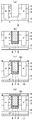
- FIG. 3 is a cross-sectional view showing a manufacturing process of the SiC semiconductor device shown in FIG. 1.
- FIG. 3 is a cross-sectional view showing a manufacturing step of the SiC semiconductor device following FIG. 2.
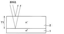
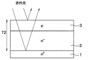
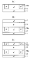
- FIG. 5 is a cross-sectional view showing a state of measuring a film thickness of an n ⁇ type drift layer. It is sectional drawing which showed the mode of the film thickness measurement of a p-type base area
- the SiC semiconductor device according to the present embodiment has a MOSFET formed thereon.
- the MOSFET is formed in the cell region of the SiC semiconductor device, and the SiC semiconductor device is configured by forming the outer peripheral withstand voltage structure so as to surround the cell region.
- the MOSFET is illustrated here. is there.
- an n + type substrate 1 made of SiC is used as a semiconductor substrate.
- An n ⁇ type drift layer 2 made of SiC, a p type base region 3 and an n + type source region 4 are epitaxially grown in this order on the main surface of the n + type substrate 1.
- the n + type substrate 1 has an n-type impurity concentration of 1.0 ⁇ 10 19 / cm 3 and a surface of a (0001) Si surface.
- the n ⁇ -type drift layer 2 has an n-type impurity concentration of 0.5 to 2.0 ⁇ 10 16 / cm 3 and a thickness of 5 to 14 ⁇ m.
- the p-type base region 3 is a portion where a channel region is formed, and has a p-type impurity concentration of, for example, about 2.0 ⁇ 10 17 / cm 3 and a thickness of 0.5 to 2 ⁇ m.
- the n + -type source region 4 has a higher impurity concentration than the n ⁇ -type drift layer 2, and the n-type impurity concentration in the surface layer portion is, for example, 2.5 ⁇ 10 18 to 1.0 ⁇ 10 19 / cm 3 and has a thickness. It is composed of about 0.5 to 2 ⁇ m.
- the film thicknesses of the n ⁇ -type drift layer 2, the p-type base region 3 and the n + -type source region 4 are arbitrarily set, but the total film thickness thereof is set in the range of 5 to 16 ⁇ m. ing.
- a p-type deep layer 5 is formed so as to penetrate the n + -type source region 4 and the p-type base region 3 and reach the n ⁇ -type drift layer 2.
- the p-type deep layer 5 has a higher p-type impurity concentration than the p-type base region 3.
- a plurality of p-type deep layers 5 are arranged at equal intervals on the n ⁇ -type drift layer 2 and are spaced apart from each other so that the top surface layout is striped.
- each p-type deep layer 5 has a p-type impurity concentration of, for example, 1.0 ⁇ 10 17 to 1.0 ⁇ 10 19 / cm 3 , a width of 0.7 ⁇ m, and a depth of p-type base region 3 and n + -type. It is configured to be deeper than the total film thickness of the source region 4 by 0.4 ⁇ m or more.
- the width is 0.8 ⁇ m and the depth is the p-type base region 3 and the n + -type source region so as to penetrate the p-type base region 3 and the n + -type source region 4 and reach the n ⁇ -type drift layer 2.
- a gate trench 6 that is deeper by 0.2 to 0.4 ⁇ m than the total thickness of 4 is formed.
- the p-type base region 3 and the n + -type source region 4 described above are arranged so as to be in contact with the side surface of the gate trench 6.
- the gate trench 6 is formed in a line-shaped layout in which the horizontal direction in FIG. 1 is the width direction, the normal direction to the longitudinal direction is the longitudinal direction, and the vertical direction is the depth direction.
- gate trench 6 Although only one gate trench 6 is shown in FIG. 1, a plurality of gate trenches 6 are arranged at equal intervals in the left-right direction on the paper surface, and are arranged so as to be sandwiched between p-type deep layers 5 respectively. It is made into a shape.
- a portion of the p-type base region 3 located on the side surface of the gate trench 6 is used as a channel region that connects the n + -type source region 4 and the n ⁇ -type drift layer 2 when the vertical MOSFET is operated.
- a gate insulating film 7 is formed on the inner wall surface of the gate trench 6 including the channel region.
- a gate electrode 8 made of doped Poly-Si is formed on the surface of the gate insulating film 7, and the gate trench 6 is completely filled with the gate insulating film 7 and the gate electrode 8.
- a source electrode 9 corresponding to the first electrode is formed on the surface of the n + -type source region 4 and the p-type deep layer 5 and the surface of the gate electrode 8 with an interlayer insulating film 10 interposed therebetween.
- the source electrode 9 and the like are made of a plurality of metals, such as Ni / Al.
- the plurality of metals at least the n-type SiC, specifically, the n + -type source region 4 and the portion in contact with the gate electrode 8 in the case of n-type doping are made of a metal capable of ohmic contact with the n-type SiC. Yes.
- At least a portion of the plurality of metals that contacts the p-type SiC, specifically, the p-type deep layer 5, is made of a metal that can make ohmic contact with the p-type SiC.
- the source electrode 9 and the like are electrically insulated by being formed on the interlayer insulating film 10. The source electrode 9 is in electrical contact with the n + -type source region 4 and the p-type deep layer 5 through a contact hole formed in the interlayer insulating film 10.
- the drain electrode 11 corresponding to the second electrode electrically connected to the n + -type substrate 1 is formed on the back side of the n + -type substrate 1 .
- an n-channel inversion type MOSFET having a trench gate structure is formed.
- a cell region is configured by arranging a plurality of such MOSFETs.
- An SiC semiconductor device is configured by forming an outer peripheral breakdown voltage structure such as a guard ring (not shown) so as to surround a cell region where such a MOSFET is formed.
- the n ⁇ type drift layer 2 formed on the n + type substrate 1 is relatively thick at 5 to 14 ⁇ m, so that the film thickness measurement by the well-known FTIR is performed. Is possible. That is, the n + type substrate 1 on which the n ⁇ type drift layer 2 is grown is irradiated with infrared light from the n ⁇ type drift layer 2 side, and the interface between the n ⁇ type drift layer 2 and the n + type substrate 1 is irradiated. And the interference light of the reflected light from the surface of the n ⁇ type drift layer 2 is measured. Then, the spectrum of each reflected light is obtained by Fourier transforming the interference light, and the film thickness of the n ⁇ -type drift layer 2 can be measured.
- the p-type base region 3 and the n + -type source region 4 formed on the n ⁇ -type drift layer 2 have a very thin film thickness of 0.5 to 2.0 ⁇ m.
- the film thickness of the p-type base region 3 cannot be measured by reflection from the interface between the n ⁇ -type drift layer 2 and the p-type base region 3 serving as a base or from the surface of the p-type base region 3.
- the amount of protrusion from the bottom surface of the p-type base region 3 of the gate trench 6 formed from the surface of the n + -type source region 4 can be accurately set, for example, within a range of 0.2 to 0.4 ⁇ m. Is possible. If the protruding amount of the gate trench 6 is too large, the distance from the n + -type substrate 1 is shortened and the breakdown voltage against the reverse bias is reduced. Therefore, the reliability with respect to the reverse bias can be ensured by being within the above range. . Therefore, a low on-resistance can be achieved by setting the thickness of the p-type base region 3 accurately, and a high reverse bias reliability can be ensured by setting the protruding amount of the gate trench 6 accurately.
- an n + type substrate 1 is prepared as a semiconductor substrate. Then, an n ⁇ type drift layer 2 made of SiC, a p type base region 3 and an n + type source region 4 are epitaxially grown on the main surface of the n + type substrate 1 in this order. At this time, when the n ⁇ -type drift layer 2, the p-type base region 3, and the n + -type source region 4 are formed, a process of measuring each film thickness is performed.
- n - n after forming the type drift layer 2 in a film thickness of 5 ⁇ 14 [mu] m - -type drift layer 2 having a thickness (hereinafter, even as thickness T1) performs the step of measuring. Specifically, as shown in FIG. 4, n - infrared light irradiated from the type drift layer 2 side, n - - type n drift layer 2 with respect to n + -type substrate 1 having grown -type drift layer The interference light of the reflected light from the interface between 2 and the n + type substrate 1 and the surface of the n ⁇ type drift layer 2 is measured. And the spectrum of each reflected light is obtained by carrying out the Fourier transform of the interference light, and the film thickness T1 can be further measured. At this time, since the n ⁇ -type drift layer 2 is formed with a film thickness of 5 to 14 ⁇ m, the film thickness T1 can be accurately measured by FTIR, and the film thickness can be accurately determined. Can be confirmed.
- a film thickness measurement step for the p-type base region 3 is performed. Specifically, as shown in FIG. 5, infrared light is irradiated from the p-type base region 3 side to the n + -type substrate 1 on which the p-type base region 3 and the n ⁇ -type drift layer 2 are grown.
- the film thickness of the p-type base region 3 can be calculated by calculating T2-T1 obtained by subtracting the one-layer film thickness T1 measured earlier from the two-layer film thickness T2.
- the repeatability is required for the FTIR film thickness measurement.
- the repeatability means that when the thin film is formed on the base, there is less variation in measurement results when the film thickness of the thin film is repeatedly measured. If the repeatability is high and the variation in measurement results is small, the film thickness measurement accuracy when a thin film is formed is high.
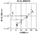
- the result shown in FIG. 6 was obtained. Specifically, a substrate on which an epitaxial film having an in-plane average film thickness of about 2 ⁇ m, 6 ⁇ m, 10 ⁇ m, 16 ⁇ m, and 22 ⁇ m was prepared, and the film thickness of the epitaxial film was repeatedly measured by FTIR. As a result, when the average film thickness was 2 ⁇ m or 20 ⁇ m, the repeatability was about 0.02 ⁇ m, but between 5 and 16 ⁇ m, the repeatability was 0.01 or less. In particular, when the average film thickness is between 5 and 10 ⁇ m, the repeatability is as high as 0.005 ⁇ m or less.
- the thickness of the epitaxial film to be measured is in the range of at least 5 to 16 ⁇ m, high repeatability can be obtained, and the thickness measurement accuracy when the epitaxial film is formed is 0. It can be seen that it can be suppressed to 0.01 ⁇ m.
- the measurement accuracy of the thickness T1 can be suppressed to 0.01 ⁇ m at the maximum.
- the film thickness measurement accuracy of the two-layer film thickness T2 can be suppressed to 0.01 ⁇ m at the maximum. Therefore, since the maximum film thickness measurement accuracy of the two-layer film thickness T2 is 0.01 ⁇ m and the one-layer film thickness T1 is a maximum film thickness measurement accuracy of 0.01 ⁇ m, the one-layer film thickness T1 is subtracted from the two-layer film thickness T2. The film thickness measurement accuracy of the obtained p-type base region 3 is 0.02 ⁇ m at the maximum.
- the film thickness of the p-type base region 3 can be evaluated with a film thickness measurement accuracy of 0.02 ⁇ m or less.
- the mold base region 3 can have a desired film thickness.
- the thickness of the n ⁇ -type drift layer 2 is set within a range of 5 to 10 ⁇ m, and the total thickness of the n ⁇ -type drift layer 2 and the p-type base region 3 is also set within a range of 5 to 10 ⁇ m.
- the film thickness measurement accuracy of the single layer thickness T1 and the double layer thickness T2 is 0.005 ⁇ m at the maximum. Therefore, in this case, it becomes possible to evaluate the film thickness of the p-type base region 3 with a film thickness measurement accuracy of 0.01 ⁇ m or less, and to make the p-type base region 3 a desired film thickness with higher accuracy. Is possible.
- an n + -type source region 4 is formed on the p-type base region 3 to a thickness of 0.5 to 2.0 ⁇ m. Then, a film thickness measurement process of the n + type source region 4 is performed. In this case, the n + -type source region infrared light irradiated from the 4 side, rather than the reflected light at the interface between the n + -type source region 4 and the p-type base region 3, n - -type drift layer 2 and the n + The interference light of the reflected light from the interface with the mold substrate 1 and the reflected light from the surface of the n + type source region 4 is measured.
- the film thickness of the n + -type source region 4 can be calculated by calculating T3 ⁇ T2 obtained by subtracting the two-layer film thickness T2 measured previously from the three-layer film thickness T3.
- the n + type source region 4 can have a desired film thickness.
- the two-layer film thickness T2 is set within the range of 5 to 10 ⁇ m and the three-layer film thickness T3 is also within the range of 5 to 10 ⁇ m, the variation between the two-layer film thickness T2 and the three-layer film thickness T3. Is 0.005 ⁇ m at the maximum. Therefore, in this case, it is possible to evaluate the thickness of the n + -type source region 4 with the following film thickness measurement accuracy 0.01 [mu] m, and the desired thickness of the n + -type source region 4 with higher accuracy It becomes possible to do.
- the n ⁇ type drift layer 2 the p type base region 3 and the n + type source region 4, it is possible to form them with a film thickness controlled with high precision.
- a mask (not shown) is arranged on the surface of the n + -type source region 4, and a region where the p-type deep layer 5 is to be formed in the mask is opened. Then, a trench 5a having a predetermined width is formed by performing anisotropic etching such as RIE (Reactive Ion Etching) using a mask.
- anisotropic etching such as RIE (Reactive Ion Etching)
- Step shown in FIG. 2 (c)] After removing the mask, the p-type layer 50 is formed. At this time, the p-type layer 50 is buried in the trench 5a by buried epi. However, since the trench 5a is formed in a narrow line shape, the p-type layer 50 is surely formed in the trench 5a. It becomes possible to embed in.
- Etchback is performed so that a portion of the p-type layer 50 formed above the surface of the n + -type source region 4 is removed by dry etching. Thereby, the p-type deep layer 5 is formed.
- Step shown in FIG. 3 (a) After forming a mask (not shown) on the n + -type source region 4 and the like, a region where the gate trench 6 is to be formed in the mask is opened. Then, the gate trench 6 is formed by performing anisotropic etching such as RIE using a mask.
- the p-type base region 3 and the n + -type source region 4 can be formed with a film thickness controlled with high precision. Therefore, when the gate trench 6 is formed, the p-type base region 3 It is possible to accurately set the protruding amount from the low part.
- the p-type base region 3 is 0.5 to 2 ⁇ m
- the n + -type source region 4 is 0.5 to 2 ⁇ m.
- the etching is performed such that the depth of the gate trench 6 is 0.2 to 0.4 ⁇ m deeper than the total film thickness of the p-type base region 3 and the n + -type source region 4,
- the protruding amount of the bottom of the mold base region 3 can be accurately adjusted to 0.2 to 0.4 ⁇ m.
- the gate insulating film 7 is formed by, for example, thermal oxidation, and the gate insulating film 7 covers the inner wall surface of the gate trench 6 and the surface of the n + -type source region 4. Then, after depositing Poly-Si doped with p-type impurities or n-type impurities, this is etched back to leave the Poly-Si at least in the gate trench 6 to form the gate electrode 8.
- An interlayer insulating film 10 made of, for example, an oxide film is formed so as to cover the surfaces of the gate electrode 8 and the gate insulating film 7. Then, after forming a mask (not shown) on the surface of the interlayer insulating film 10, a portion of the mask located between the gate electrodes 8, that is, a portion corresponding to the p-type deep layer 5 and its vicinity are opened. Thereafter, the interlayer insulating film 10 is patterned using a mask to form a contact hole exposing the p-type deep layer 5 and the n + -type source region 4.
- Step shown in FIG. 3 (d)] On the surface of the interlayer insulating film 10, for example, an electrode material composed of a laminated structure of a plurality of metals is formed. Then, the source electrode 9 is formed by patterning the electrode material.
- the SiC semiconductor device according to the present embodiment is completed by performing steps such as forming the drain electrode 11 on the back surface side of the n + type substrate 1.
- the p-type base region 3 and the n + -type source region 4 as in the present embodiment, these can be formed with a highly controlled film thickness. Thereby, it is possible to obtain a SiC semiconductor device in which the film thickness is accurately controlled.
- the p-type base region 3 Since the thickness of the p-type base region 3 can be set accurately, the p-type base region 3 is not formed thicker than necessary, and a low on-resistance can be achieved. Furthermore, since the film thicknesses of the p-type base region 3 and the n + -type source region 4 can be accurately set, the protruding amount of the gate trench 6 can be accurately set, and high reverse bias reliability is ensured. It becomes possible.
- the film thickness measurement of the p-type base region 3 and the n + -type source region 4 has been described.
- the film thickness measurement of the p-type deep layer 5 at the time of etch-back in other words, the etch-back amount.
- the same FTIR as in the first embodiment is used.
- the p-type layer 50 is formed to embed the p-type layer 50 in the trench 5a.
- the p-type layer 50 is also formed on the n + -type source region 4 at this time.
- FTIR is used to measure the film thickness of the p-type layer 50 on the n + -type source region 4.
- the n ⁇ type drift layer 2, the p type base region 3, and the n + type source region 4 are epitaxially grown in order on the main surface of the n + type substrate 1 in the step shown in FIG.
- the three-layer film thickness T3 is measured.
- a triple epi substrate in which an n ⁇ type drift layer 2, a p type base region 3 and an n + type source region 4 are epitaxially grown in advance on the main surface of the n + type substrate 1 may be prepared.
- the steps shown in FIGS. 2B and 2C are performed.
- p-type layer 50 is formed so as to fill trench 5a, and p-type layer 50 is also formed on n + -type source region 4.
- the film thickness measurement process of the p-type layer 50 is performed.
- the total thickness of the n ⁇ type drift layer 2, the p type base region 3, the n + type source region 4 and the p type layer 50 (hereinafter referred to as the four-layer thickness T4). Measure).
- the film thickness of the p-type layer 50 can be calculated by calculating T4-T3 obtained by subtracting the three-layer film thickness T3 from the four-layer film thickness T4.
- the n ⁇ -type drift layer 2 and the p-type base region are set so that the three-layer film thickness T3 is in the range of 5 to 16 ⁇ m and the four-layer film thickness T4 is also in the range of 5 to 16 ⁇ m. 3.
- the film thicknesses of the n + -type source region 4 and the p-type layer 50 are set. Thereby, the film thickness of the p-type layer 50 can be evaluated with a film thickness measurement accuracy of 0.02 ⁇ m or less.
- the film thickness of the p-type layer 50 can be evaluated with a film thickness measurement accuracy of 0.01 ⁇ m or less.
- the etching surface is irradiated with infrared light, and the film thickness from the interface between the n ⁇ type drift layer 2 and the n + type substrate 1 to the etching surface by FTIR (hereinafter referred to as etching surface film thickness T5). Can also be measured.
- the remaining amount of the p-type layer 50 can be grasped by calculating T5-T3 obtained by subtracting the three-layer film thickness T3 from the etching surface film thickness T5. Therefore, if the residue of the p-type layer 50 is confirmed by the measurement during the etch back, the etch back can be performed with higher accuracy by repeating the etch back again. Only the p-type layer 50 can be removed more accurately.
- the protruding amount of the gate trench 6 can be set accurately.
- a third embodiment will be described.
- the present embodiment is different from the first embodiment in that an ion implantation layer is formed before the film thickness measurement, but is otherwise the same as the first embodiment. Only the different parts will be described.
- the p-type deep layer 5 is formed by forming the p-type layer 50 in the trench 5a and etching back.
- the p-type deep layer 5 can also be formed by ion implantation.
- a mask (not shown) in which the region where the p-type deep layer 5 is to be formed is arranged to perform ion implantation.
- the lower layer portion 5b of the p-type deep layer 5 is formed.
- a p-type base region 3 is formed, and an n + -type source region 4 is further formed.
- the p-type base region and go the thickness measuring step of p-type base region 3 3 after forming, n + -type source after forming the n + -type source region 4 A film thickness measurement process in region 4 is performed. Thereby, the film thicknesses of the p-type base region 3 and the n + -type source region 4 can be accurately measured.
- a p-type deep is formed by arranging a mask (not shown) in which a region where the p-type deep layer 5 is to be formed is opened on the n + -type source region 4 and performing ion implantation.
- a contact portion 5c of the layer 5 is formed. At this time, as long as the contact portion 5c is formed so as to be in contact with at least the p-type base region 3, since it has the same conductivity type, it is electrically connected to the lower layer portion 5b. Also good.
- the p-type deep layer 5 can also be formed by ion implantation.
- an ion implantation layer is formed thereunder.
- the film thickness may not be measured.
- the p-type base is accurately obtained regardless of whether or not the ion implantation layer is formed.
- the film thickness of the region 3 and the film thickness of the n + -type source region 4 can be measured.
- the n + type substrate 1 is used as the base layer
- the n ⁇ type drift layer 2 is used as the first epitaxial film
- the p type base region 3 is used as the second epitaxial film.
- the above-described FTIR is used when measuring the thickness of the second epitaxial film.
- the film thickness measurement step can be performed.
- the n + -type source region 4 is taken as an example of the third epitaxial film, this is just an example.
- the above-described film thickness measurement process by FTIR can be performed.
- the one-layer film thickness T1 corresponds to the first film thickness
- the two-layer film thickness T2 corresponds to the second film thickness
- the three-layer film thickness T3 corresponds to the third film thickness.
- the n + -type substrate 1 is used as the base, the n ⁇ -type drift layer 2 and the p-type base region 3 and the n + -type source region 4 are stacked as the first epitaxial film, and the second epitaxial film is used.
- the p-type layer 50 is taken as an example. However, this is merely an example, and the thickness of the second epitaxial film is measured in a structure in which the first epitaxial film is formed on the base layer and the second epitaxial film is stacked thereon. In some cases, the film thickness measurement step by FTIR can be performed.
- the three-layer film thickness T3 corresponds to the first film thickness
- the four-layer film thickness T4 corresponds to the second film thickness.
- the film thickness is measured by FTIR after the n ⁇ type drift layer 2, the p type base region 3 and the n + type source region 4 are formed.
- a film thickness measurement mechanism by FTIR is provided in the epitaxial growth apparatus for forming the n ⁇ type drift layer 2, the p type base region 3 and the n + type source region 4, these components are formed. It is also possible to measure each film thickness in the film. As a result, the film thickness can be controlled more accurately.
- the film thickness is measured by FTIR after the p-type layer 50 is etched back.
- the film thickness can be measured during the etching of the p-type layer 50. Become. As a result, the film thickness can be controlled more accurately.
- the MOSFET is described as an example of the element provided in the SiC semiconductor device.
- the element is not limited to the MOSFET, and another element may be formed.
- the n-channel type MOSFET in which the first conductivity type is n-type and the second conductivity type is p-type has been described as an example, but a p-channel type MOSFET in which the conductivity type of each component is inverted may be used. good.
- the MOSFET has been described as an example of the semiconductor element.
- the present disclosure can be applied to an IGBT having a similar structure.
- the IGBT only changes the conductivity type of the n + type substrate 1 from the n-type to the p-type with respect to the above-described embodiments, and the other structures and manufacturing methods are the same as those in the above-described embodiments.
- the vertical MOSFET having the trench gate structure has been described as an example. However, the vertical MOSFET is not limited to the trench gate structure but may be a planar type.
Landscapes
- Physics & Mathematics (AREA)
- General Physics & Mathematics (AREA)
- Testing Or Measuring Of Semiconductors Or The Like (AREA)
Abstract
p型ベース領域(3)の膜厚を測定する際に、p型ベース領域(3)およびn-型ドリフト層(2)を成長させたn+型基板(1)に対してp型ベース領域(3)側から赤外光を照射する。そして、p型ベース領域(3)とn-型ドリフト層(2)との界面の反射光ではなく、n-型ドリフト層(2)とn+型基板(1)との界面の反射光およびp型ベース領域(3)の表面からの反射光の干渉光を測定する。このようにすれば、p型ベース領域(3)とn-型ドリフト層(2)との合計膜厚である二層膜厚T2を測定することが可能となる。したがって、二層膜厚T2からn-型ドリフト層(2)である一層膜厚T1を差し引いたT2-T1を演算することで、p型ベース領域(3)の膜厚を算出することができる。
Description
本出願は、2016年8月31日に出願された日本特許出願番号2016-169815号に基づくもので、ここにその記載内容が参照により組み入れられる。
本開示は、炭化珪素(以下、SiCという)半導体装置およびその製造方法に関するものである。
半導体装置の製造の際には、各部の膜厚が適正な値となるように、膜厚測定が行われている。その膜厚測定には、フーリエ変換赤外分光法(以下、略してFTIRという)が用いられている(例えば、特許文献1参照)。FTIRでは、例えば膜厚測定の対象となる薄膜に対して赤外光を照射すると共に、下地と薄膜との界面や薄膜の表面からの反射光の干渉光を測定し、干渉光をフーリエ変換することで各反射光のスペクトルを得て、薄膜の膜厚測定を行う。
しかしながら、FTIRではある程度決まった膜厚範囲でないと膜厚測定を行うことができないため、SiC半導体装置のように、イオン注入層やエピタキシャル層が複数存在する構成においては、各層の膜厚を的確に測定することが困難である。特に、エピタキシャル膜を下地となるSiCの上に形成する場合、下地となるSiCとエピタキシャル膜の不純物濃度の差が少ないことから、エピタキシャル膜の膜厚を測定することができなかった。また、膜厚評価目的で付加的にエピタキシャル膜のないモニタ基板を用いる場合にも測定対象となる薄膜の目標膜厚が薄いと、センターバースト領域と重なって正確なスペクトルを得ることができず、さらに高精度な膜厚測定を行うことが困難になる。このため、所望の膜厚に制御されたSiC半導体装置を得ることができなかった。
本開示は、的確に膜厚制御が行われたSiC半導体装置およびその製造方法を提供することを目的とする。
本開示の1つの観点におけるSiC半導体装置の製造方法では、炭化珪素にて形成された下地層上に、5~14μmの厚みの第1エピタキシャル膜が形成された構造を用意することと、第1エピタキシャル膜の表面側から赤外光を照射し、第1エピタキシャル膜と下地層との界面からの反射光と第1エピタキシャル膜の表面からの反射光とに基づいて、FTIRによって第1エピタキシャル膜の膜厚となる第1膜厚を測定することと、第1エピタキシャル膜の上に0.5~2.0μmの厚みの第2エピタキシャル膜を形成することと、第2エピタキシャル膜の表面側から赤外光を照射し、第1エピタキシャル膜と下地層との界面からの反射光と第2エピタキシャル膜の表面からの反射光とに基づいて、フーリエ変換赤外分光法によって第1エピタキシャル膜と第2エピタキシャル膜の合計膜厚となる第2膜厚を測定することと、第2膜厚から第1膜厚を差し引くことで第2エピタキシャル膜の膜厚を算出することと、を含んでいる。
このように、5~14μmの厚みの第1エピタキシャル膜の上に0.5~2.0μmの厚みの第2エピタキシャル膜を形成する場合、高い精度で第1膜厚を測定しつつ、第2膜厚を測定できる。このため、第2膜厚から第1膜厚を差し引くことで第2エピタキシャル膜の膜厚を精度良く算出することが可能となる。したがって、的確に膜厚制御が行われたSiC半導体装置を製造することができる。
本開示のもう1つの観点としてのSiC半導体装置の製造方法では、炭化珪素にて形成された下地層上に、5~14μmの厚みの第1エピタキシャル膜が形成された構造を用意することと、第1エピタキシャル膜の表面側から赤外光を照射し、第1エピタキシャル膜と下地層との界面からの反射光と第1エピタキシャル膜の表面からの反射光とに基づいて、フーリエ変換赤外分光法によって第1エピタキシャル膜の膜厚となる第1膜厚を測定することと、第1エピタキシャル膜の上に0.5~2.0μmの厚みの第2エピタキシャル膜を成長させることと、第2エピタキシャル膜の表面側から赤外光を照射し、第1エピタキシャル膜と下地層との界面からの反射光と第2エピタキシャル膜の表面からの反射光とに基づいて、フーリエ変換赤外分光法によって第1エピタキシャル膜と第2エピタキシャル膜の合計膜厚となる第2膜厚を測定することと、第2膜厚から第1膜厚を差し引くことで第2エピタキシャル膜の膜厚を算出することと、算出された膜厚分、第2エピタキシャル膜をエッチバックして除去することと、を含んでいる。
このように、第2エピタキシャル膜をエッチバックする場合にも、第2エピタキシャル膜の膜厚を精度良く測定できることが必要である。この場合にも、5~14μmの厚みの第1エピタキシャル膜の上に0.5~2.0μmの厚みの第2エピタキシャル膜を形成する場合、高い精度で第1膜厚を測定しつつ、第2膜厚を測定できる。このため、第2膜厚から第1膜厚を差し引くことで第2エピタキシャル膜の膜厚を精度良く算出することが可能となる。したがって、的確に第2エピタキシャル膜の膜厚分をエッチバックでき、的確に膜厚制御が行われたSiC半導体装置を製造することができる。
以下、本開示の実施形態について図に基づいて説明する。なお、以下の各実施形態相互において、互いに同一もしくは均等である部分には、同一符号を付して説明を行う。
(第1実施形態)
第1実施形態について説明する。本実施形態にかかるSiC半導体装置は、図1に示すように、MOSFETが形成されたものである。MOSFETは、SiC半導体装置のうちのセル領域に形成されており、そのセル領域を囲むように外周耐圧構造が形成されることでSiC半導体装置が構成されているが、ここではMOSFETのみ図示してある。
第1実施形態について説明する。本実施形態にかかるSiC半導体装置は、図1に示すように、MOSFETが形成されたものである。MOSFETは、SiC半導体装置のうちのセル領域に形成されており、そのセル領域を囲むように外周耐圧構造が形成されることでSiC半導体装置が構成されているが、ここではMOSFETのみ図示してある。
SiC半導体装置には、SiCからなるn+型基板1が半導体基板として用いられている。n+型基板1の主表面上にSiCからなるn-型ドリフト層2、p型ベース領域3およびn+型ソース領域4が順にエピタキシャル成長させられている。
n+型基板1は、例えばn型不純物濃度が1.0×10¹⁹/cm3とされ、表面が(0001)Si面とされている。n-型ドリフト層2は、例えばn型不純物濃度が0.5~2.0×1016/cm3とされ、厚さが5~14μmとされている。
また、p型ベース領域3は、チャネル領域が形成される部分で、p型不純物濃度が例えば2.0×10¹⁷/cm3程度とされ、厚みが0.5~2μmで構成されている。n+型ソース領域4は、n-型ドリフト層2よりも高不純物濃度とされ、表層部におけるn型不純物濃度が例えば2.5×1018~1.0×1019/cm3、厚さ0.5~2μm程度で構成されている。なお、n-型ドリフト層2、p型ベース領域3およびn+型ソース領域4の膜厚については任意に設定してあるが、これらの合計膜厚が5~16μmの範囲内となるようにしている。
n+型ソース領域4やp型ベース領域3を貫通してn-型ドリフト層2に達するようにp型ディープ層5が形成されている。p型ディープ層5は、p型ベース領域3よりもp型不純物濃度が高くされている。具体的には、p型ディープ層5は、n-型ドリフト層2に複数本が等間隔に配置され、互いに交点なく離れて配置されることで、上面レイアウトがストライプ状とされている。例えば、各p型ディープ層5は、p型不純物濃度が例えば1.0×10¹⁷~1.0×10¹⁹/cm3、幅0.7μm、深さがp型ベース領域3とn+型ソース領域4の合計膜厚よりも0.4μm以上深くなるように構成されている。
また、p型ベース領域3およびn+型ソース領域4を貫通してn-型ドリフト層2に達するように、例えば幅が0.8μm、深さがp型ベース領域3とn+型ソース領域4の合計膜厚よりも0.2~0.4μm深くされたゲートトレンチ6が形成されている。このゲートトレンチ6の側面と接するように上述したp型ベース領域3およびn+型ソース領域4が配置されている。ゲートトレンチ6は、図1の紙面左右方向を幅方向、紙面法線方向を長手方向、紙面上下方向を深さ方向とするライン状のレイアウトで形成されている。また、図1には1本しか示していないが、ゲートトレンチ6は、複数本が紙面左右方向に等間隔に配置され、それぞれp型ディープ層5の間に挟まれるように配置されていてストライプ状とされている。
さらに、p型ベース領域3のうちゲートトレンチ6の側面に位置している部分を、縦型MOSFETの作動時にn+型ソース領域4とn-型ドリフト層2との間を繋ぐチャネル領域として、チャネル領域を含むゲートトレンチ6の内壁面にゲート絶縁膜7が形成されている。そして、ゲート絶縁膜7の表面にはドープドPoly-Siにて構成されたゲート電極8が形成されており、これらゲート絶縁膜7およびゲート電極8によってゲートトレンチ6内が埋め尽くされている。
また、n+型ソース領域4およびp型ディープ層5の表面やゲート電極8の表面には、層間絶縁膜10を介して第1電極に相当するソース電極9などが形成されている。ソース電極9などは、複数の金属、例えばNi/Al等にて構成されている。そして、複数の金属のうち少なくともn型SiC、具体的にはn+型ソース領域4やn型ドープの場合のゲート電極8と接触する部分はn型SiCとオーミック接触可能な金属で構成されている。また、複数の金属のうち少なくともp型SiC、具体的にはp型ディープ層5と接触する部分はp型SiCとオーミック接触可能な金属で構成されている。なお、ソース電極9などは、層間絶縁膜10上に形成されることで電気的に絶縁されている。そして、層間絶縁膜10に形成されたコンタクトホールを通じて、ソース電極9はn+型ソース領域4およびp型ディープ層5と電気的に接触させられている。
さらに、n+型基板1の裏面側にはn+型基板1と電気的に接続された第2電極に相当するドレイン電極11が形成されている。このような構造により、nチャネルタイプの反転型のトレンチゲート構造のMOSFETが構成されている。このようなMOSFETが複数セル配置されることでセル領域が構成されている。そして、このようなMOSFETが形成されたセル領域を囲むように図示しないガードリングなどによる外周耐圧構造が構成されることでSiC半導体装置が構成されている。
このように構成されたSiC半導体装置では、n+型基板1の上に形成されるn-型ドリフト層2については5~14μmと比較的厚いことから、周知のFTIRによる膜厚測定を行うことが可能となる。すなわち、n-型ドリフト層2を成長させたn+型基板1に対してn-型ドリフト層2側から赤外光を照射し、n-型ドリフト層2とn+型基板1との界面およびn-型ドリフト層2の表面からの反射光の干渉光を測定する。そして、その干渉光をフーリエ変換することで各反射光のスペクトルを得て、n-型ドリフト層2の膜厚測定を行うことができる。
ところが、n-型ドリフト層2の上に形成されるp型ベース領域3およびn+型ソース領域4については、0.5~2.0μmと非常に膜厚が薄い。このため、p型ベース領域3については、下地となるn-型ドリフト層2とp型ベース領域3との界面やp型ベース領域3の表面からの反射によって膜厚を測定することができない。同様に、n+型ソース領域4については、下地となるp型ベース領域3とn+型ソース領域4との界面やn+型ソース領域4の表面からの反射によって膜厚を測定することができない。
しかしながら、後述する手法によってp型ベース領域3とn+型ソース領域4の膜厚を測定することで、これらを小さな膜厚バラツキで形成できている。このため、n+型ソース領域4の表面から形成されるゲートトレンチ6のp型ベース領域3の底面からの突き出し量を正確に設定でき、例えば0.2~0.4μmの範囲内に収めることが可能となる。ゲートトレンチ6の突き出し量は、大きすぎるとn+型基板1からの距離が短くなって逆バイアスに対する耐圧低下に繋がることから、上記範囲内に収められることで、逆バイアスに対する信頼性を確保できる。よって、p型ベース領域3の厚みを的確に設定できることで低オン抵抗が図れ、かつ、ゲートトレンチ6の突き出し量を的確に設定できることで高逆バイアス信頼性を確保することも可能となる。
次に、本実施形態にかかるnチャネルタイプの反転型のトレンチゲート構造のMOSFETを備えたSiC半導体装置の製造方法について、図2および図3に示す製造工程中の断面図を参照して説明する。
〔図2(a)に示す工程〕
まず、半導体基板として、n+型基板1を用意する。そして、このn+型基板1の主表面上にSiCからなるn-型ドリフト層2、p型ベース領域3およびn+型ソース領域4を順にエピタキシャル成長させる。このとき、n-型ドリフト層2、p型ベース領域3およびn+型ソース領域4を成膜する際に、それぞれの膜厚を計測する工程を行っている。
まず、半導体基板として、n+型基板1を用意する。そして、このn+型基板1の主表面上にSiCからなるn-型ドリフト層2、p型ベース領域3およびn+型ソース領域4を順にエピタキシャル成長させる。このとき、n-型ドリフト層2、p型ベース領域3およびn+型ソース領域4を成膜する際に、それぞれの膜厚を計測する工程を行っている。
まず、n-型ドリフト層2を5~14μmの膜厚で成膜したのちn-型ドリフト層2の膜厚(以下、一層膜厚T1という)の測定工程を行う。具体的には、図4に示すように、n-型ドリフト層2を成長させたn+型基板1に対してn-型ドリフト層2側から赤外光を照射し、n-型ドリフト層2とn+型基板1との界面およびn-型ドリフト層2の表面からの反射光の干渉光を測定する。そして、その干渉光をフーリエ変換することで各反射光のスペクトルを得て、一層膜厚T1の測定を行うことができる。このとき、n-型ドリフト層2を5~14μmの膜厚で形成していることから、FTIRによって一層膜厚T1を的確に測定することができ、所望の膜厚になっていることを的確に確認することができる。
続いて、n-型ドリフト層2の上にp型ベース領域3を0.5~2μm成膜したのちp型ベース領域3の膜厚測定工程を行う。具体的には、図5に示すように、p型ベース領域3およびn-型ドリフト層2を成長させたn+型基板1に対してp型ベース領域3側から赤外光を照射する。そして、p型ベース領域3とn-型ドリフト層2との界面の反射光ではなく、n-型ドリフト層2とn+型基板1との界面の反射光およびp型ベース領域3の表面からの反射光の干渉光を測定する。このようにすれば、p型ベース領域3とn-型ドリフト層2との合計膜厚(以下、二層膜厚T2という)を測定することが可能となる。したがって、二層膜厚T2から先ほど測定した一層膜厚T1を差し引いたT2-T1を演算することで、p型ベース領域3の膜厚を算出することができる。
ここで、FTIRの膜厚測定については、繰り返し精度が求められる。繰り返し精度とは、下地上に薄膜を成膜ときに、繰り返し薄膜の膜厚測定を行ったときの測定結果のバラツキが少なくなることを意味している。繰り返し精度が高く、測定結果のバラツキが小さければ、薄膜を成膜したときの膜厚測定精度が高い。
この繰り返し精度の膜厚依存性について調べたところ、図6に示す結果が得られた。具体的には、面内における平均膜厚がおよそ2μm、6μm、10μm、16μm、22μmとなるエピタキシャル膜を成膜した基板を用意し、FTIRにて繰り返しエピタキシャル膜の膜厚測定を行った。その結果、平均膜厚が2μmや20μmの場合には、繰り返し精度が0.02μm程度となったが、5~16μmの間においては繰り返し精度が0.01以下となった。特に、平均膜厚が5~10μmの間においては、繰り返し精度が0.005μm以下という高い精度となった。
この結果より、測定対象となるエピタキシャル膜の膜厚が少なくとも5~16μmの範囲内であれば、高い繰り返し精度を得ることが可能と言え、エピタキシャル膜を成膜したときの膜厚測定精度を0.01μmに抑えることが可能になることが判る。そして、n-型ドリフト層2を5~14μmの膜厚に設定することで、一層膜厚T1の測定精度を最大でも0.01μmに抑えることができる。
さらに、n-型ドリフト層2の上にp型ベース領域3を成膜したとき、p型ベース領域3が0.5~2μmの膜厚であることから、二層膜厚T2が14.5~16μmとなる。このため、二層膜厚T2の膜厚測定精度についても最大でも0.01μmに抑えることができる。したがって、二層膜厚T2の膜厚測定精度が最大0.01μm、一層膜厚T1の膜厚測定精度が最大0.01μmであることから、二層膜厚T2から一層膜厚T1を差し引いて得られるp型ベース領域3の膜厚測定精度は最大でも0.02μmとなる。
よって、このような手法によってp型ベース領域3の膜厚の測定工程を行うことで、p型ベース領域3の膜厚を0.02μm以下の膜厚測定精度で評価することが可能となり、p型ベース領域3を所望の膜厚とすることが可能となる。
さらに、n-型ドリフト層2の膜厚を5~10μmの範囲内とし、かつ、n-型ドリフト層2とp型ベース領域3の合計膜厚も5~10μmの範囲内となるようにすれば、一層膜厚T1と二層膜厚T2の膜厚測定精度がそれぞれ最大でも0.005μmとなる。したがって、この場合には、p型ベース領域3の膜厚を0.01μm以下の膜厚測定精度で評価することが可能となり、より高い精度でp型ベース領域3を所望の膜厚とすることが可能となる。
この後、p型ベース領域3の上にn+型ソース領域4を0.5~2.0μm成膜する。そして、n+型ソース領域4の膜厚測定工程を行う。この場合にも、n+型ソース領域4側から赤外光を照射し、n+型ソース領域4とp型ベース領域3との界面の反射光ではなく、n-型ドリフト層2とn+型基板1との界面の反射光およびn+型ソース領域4の表面からの反射光の干渉光を測定する。このようにすれば、n+型ソース領域4とp型ベース領域3およびn-型ドリフト層2との合計膜厚(以下、三層膜厚T3という)を測定することが可能となる。したがって、三層膜厚T3から先ほど測定した二層膜厚T2を差し引いたT3-T2を演算することで、n+型ソース領域4の膜厚を算出することができる。
このとき、三層膜厚T3が5~16μmの範囲内となるように、n-型ドリフト層2やp型ベース領域3およびn+型ソース領域4それぞれの膜厚を設定すれば、n+型ソース領域4の膜厚を0.02μm以下の膜厚測定精度で評価することが可能となる。したがって、n+型ソース領域4を所望の膜厚とすることが可能となる。
さらに、二層膜厚T2を5~10μmの範囲内とし、かつ、三層膜厚T3も5~10μmの範囲内となるようにすれば、二層膜厚T2と三層膜厚T3のバラツキがそれぞれ最大でも0.005μmとなる。したがって、この場合には、n+型ソース領域4の膜厚を0.01μm以下の膜厚測定精度で評価することが可能となり、より高い精度でn+型ソース領域4を所望の膜厚とすることが可能となる。
このようにして、n-型ドリフト層2、p型ベース領域3およびn+型ソース領域4を成膜することで、これらを高精度制御された膜厚で形成することが可能となる。
〔図2(b)に示す工程〕
次に、n+型ソース領域4の表面に図示しないマスクを配置し、マスクのうちのp型ディープ層5の形成予定領域を開口させる。そして、マスクを用いてRIE(Reactive IonEtching)などの異方性エッチングを行うことにより、所定幅のトレンチ5aを形成する。
次に、n+型ソース領域4の表面に図示しないマスクを配置し、マスクのうちのp型ディープ層5の形成予定領域を開口させる。そして、マスクを用いてRIE(Reactive IonEtching)などの異方性エッチングを行うことにより、所定幅のトレンチ5aを形成する。
〔図2(c)に示す工程〕
マスクを除去した後、p型層50を成膜する。このとき、埋込エピにより、トレンチ5a内にp型層50が埋め込まれることになるが、トレンチ5aを幅が狭いライン状で形成していることから、トレンチ5a内にp型層50を確実に埋め込むことが可能になる。
マスクを除去した後、p型層50を成膜する。このとき、埋込エピにより、トレンチ5a内にp型層50が埋め込まれることになるが、トレンチ5aを幅が狭いライン状で形成していることから、トレンチ5a内にp型層50を確実に埋め込むことが可能になる。
〔図2(d)に示す工程〕
ドライエッチングによってp型層50のうちn+型ソース領域4の表面より上に形成された部分が取り除かれるようにエッチバックする。これにより、p型ディープ層5が形成される。
ドライエッチングによってp型層50のうちn+型ソース領域4の表面より上に形成された部分が取り除かれるようにエッチバックする。これにより、p型ディープ層5が形成される。
〔図3(a)に示す工程〕
n+型ソース領域4などの上に図示しないマスクを形成したのち、マスクのうちのゲートトレンチ6の形成予定領域を開口させる。そして、マスクを用いてRIEなどの異方性エッチングを行うことで、ゲートトレンチ6を形成する。
n+型ソース領域4などの上に図示しないマスクを形成したのち、マスクのうちのゲートトレンチ6の形成予定領域を開口させる。そして、マスクを用いてRIEなどの異方性エッチングを行うことで、ゲートトレンチ6を形成する。
このとき、上記したようにp型ベース領域3やn+型ソース領域4を高精度制御された膜厚で形成できていることから、ゲートトレンチ6を形成したときに、p型ベース領域3の低部からの突き出し量を正確に設定することが可能となる。例えば、上記したようにp型ベース領域3を0.5~2μmとし、n+型ソース領域4を0.5~2μmとしている。このため、ゲートトレンチ6の深さをp型ベース領域3とn+型ソース領域4の合計膜厚よりも0.2~0.4μm深くするという設定としてエッチングを行えば、ゲートトレンチ6のp型ベース領域3の底部の突き出し量を0.2~0.4μmに的確に調整できる。
〔図3(b)に示す工程〕
マスクを除去した後、例えば熱酸化を行うことによって、ゲート絶縁膜7を形成し、ゲート絶縁膜7によってゲートトレンチ6の内壁面上およびn+型ソース領域4の表面上を覆う。そして、p型不純物もしくはn型不純物がドープされたPoly-Siをデポジションした後、これをエッチバックし、少なくともゲートトレンチ6内にPoly-Siを残すことでゲート電極8を形成する。
マスクを除去した後、例えば熱酸化を行うことによって、ゲート絶縁膜7を形成し、ゲート絶縁膜7によってゲートトレンチ6の内壁面上およびn+型ソース領域4の表面上を覆う。そして、p型不純物もしくはn型不純物がドープされたPoly-Siをデポジションした後、これをエッチバックし、少なくともゲートトレンチ6内にPoly-Siを残すことでゲート電極8を形成する。
〔図3(c)に示す工程〕
ゲート電極8およびゲート絶縁膜7の表面を覆うように、例えば酸化膜などによって構成される層間絶縁膜10を形成する。そして、層間絶縁膜10の表面上に図示しないマスクを形成したのち、マスクのうち各ゲート電極8の間に位置する部分、つまりp型ディープ層5と対応する部分およびその近傍を開口させる。この後、マスクを用いて層間絶縁膜10をパターニングすることでp型ディープ層5およびn+型ソース領域4を露出させるコンタクトホールを形成する。
ゲート電極8およびゲート絶縁膜7の表面を覆うように、例えば酸化膜などによって構成される層間絶縁膜10を形成する。そして、層間絶縁膜10の表面上に図示しないマスクを形成したのち、マスクのうち各ゲート電極8の間に位置する部分、つまりp型ディープ層5と対応する部分およびその近傍を開口させる。この後、マスクを用いて層間絶縁膜10をパターニングすることでp型ディープ層5およびn+型ソース領域4を露出させるコンタクトホールを形成する。
〔図3(d)に示す工程〕
層間絶縁膜10の表面上に例えば複数の金属の積層構造により構成される電極材料を形成する。そして、電極材料をパターニングすることで、ソース電極9を形成する。
層間絶縁膜10の表面上に例えば複数の金属の積層構造により構成される電極材料を形成する。そして、電極材料をパターニングすることで、ソース電極9を形成する。
この後の工程については図示しないが、n+型基板1の裏面側にドレイン電極11を形成するなどの工程を行うことで、本実施形態にかかるSiC半導体装置が完成する。
以上説明したように、本実施形態のようにしてp型ベース領域3やn+型ソース領域4を形成することで、これらを高精度制御された膜厚で形成することができる。これにより、的確に膜厚制御が行われたSiC半導体装置とすることが可能となる。
そして、p型ベース領域3の厚みを的確に設定できることにより、p型ベース領域3を必要以上に厚く形成することが無くなり、低オン抵抗を図ることができる。さらに、p型ベース領域3やn+型ソース領域4の膜厚を的確に設定できることで、ゲートトレンチ6の突き出し量を的確に設定することが可能となって、高逆バイアス信頼性を確保することが可能となる。
(第2実施形態)
第2実施形態について説明する。本実施形態は、第1実施形態に対して膜厚測定の対象を変更したものであり、その他については第1実施形態と同様であるため、第1実施形態と異なる部分についてのみ説明する。
第2実施形態について説明する。本実施形態は、第1実施形態に対して膜厚測定の対象を変更したものであり、その他については第1実施形態と同様であるため、第1実施形態と異なる部分についてのみ説明する。
上記第1実施形態では、p型ベース領域3やn+型ソース領域4の膜厚測定について説明したが、ここではエッチバック時のp型ディープ層5の膜厚測定、換言すればエッチバック量の測定について、第1実施形態と同様のFTIRを用いる。
すなわち、第1実施形態で説明した図2(c)に示す工程において、トレンチ5aを形成した後、p型層50を成膜することでトレンチ5a内にp型層50を埋め込むようにしているが、このときにn+型ソース領域4上にもp型層50が形成されることになる。このときのn+型ソース領域4上におけるp型層50の膜厚測定にFTIRを用いる。このp型層50の膜厚を的確に測定することで、p型層50のエッチバック量を正確に規定することができる。
具体的には、図2(a)に示す工程において、n+型基板1の主表面上にn-型ドリフト層2、p型ベース領域3およびn+型ソース領域4を順にエピタキシャル成長させたときに、三層膜厚T3を測定する。このとき、予めn+型基板1の主表面上にn-型ドリフト層2、p型ベース領域3およびn+型ソース領域4を順にエピタキシャル成長させたトリプルエピ基板を用意しても良い。そして、図2(b)および図2(c)に示す工程を行う。これにより、トレンチ5a内を埋め込むようにp型層50が形成され、かつ、n+型ソース領域4の上にもp型層50が形成される。ここで、p型層50の膜厚測定工程を行う。
まず、図2(c)中に記載したように、n-型ドリフト層2、p型ベース領域3、n+型ソース領域4およびp型層50の合計膜厚(以下、四層膜厚T4という)を測定する。そして、四層膜厚T4から三層膜厚T3を差し引いたT4-T3を演算することで、p型層50の膜厚を算出することができる。
また、このとき、三層膜厚T3が5~16μmの範囲内となるようにしつつ、四層膜厚T4も5~16μmの範囲となるように、n-型ドリフト層2、p型ベース領域3、n+型ソース領域4およびp型層50それぞれの膜厚を設定する。これにより、p型層50の膜厚を0.02μm以下の膜厚測定精度で評価することが可能となる。さらに、三層膜厚T3を5~10μmの範囲内とし、かつ、四層膜厚T4も5~10μmの範囲内となるようにすれば、三層膜厚T3と四層膜厚T4のバラツキがそれぞれ最大でも0.005μmとなる。したがって、この場合には、p型層50の膜厚を0.01μm以下の膜厚測定精度で評価することが可能となる。
このため、p型層50をエッチバックする際にはエッチング時間などのエッチング条件に基づいて高い精度でn+型ソース領域4の表面からp型層50のみをその膜厚分だけ除去することが可能となる。
さらに、エッチバック時に、エッチング表面に対して赤外光を照射し、FTIRによりn-型ドリフト層2とn+型基板1との界面からエッチング表面までの膜厚(以下、エッチング表面膜厚T5という)を測定することもできる。その場合、エッチング表面膜厚T5から三層膜厚T3を差し引いたT5-T3を演算することで、p型層50の残り量を把握できる。したがって、エッチバック時の測定によってp型層50の残渣が確認されるようであれば、再びエッチバックを行うということを繰り返すようにすれば、より高い精度でエッチバックを行うことが可能となり、より的確にp型層50のみを除去することが可能となる。
これにより、エッチバック後におけるn+型ソース領域4の厚み変動を抑制でき、その結果、n+型ソース領域4の表面からゲートトレンチ6を形成するときに、p型ベース領域3の底部からのゲートトレンチ6の突き出し量を的確に設定することができる。
(第3実施形態)
第3実施形態について説明する。本実施形態は、第1実施形態に対して膜厚測定の前にイオン注入層が形成されている点が異なっているがその他については第1実施形態と同様であるため、第1実施形態と異なる部分についてのみ説明する。
第3実施形態について説明する。本実施形態は、第1実施形態に対して膜厚測定の前にイオン注入層が形成されている点が異なっているがその他については第1実施形態と同様であるため、第1実施形態と異なる部分についてのみ説明する。
上記第1実施形態では、トレンチ5aに対してp型層50を成膜し、エッチバックすることによってp型ディープ層5を形成したが、p型ディープ層5をイオン注入によって形成することもできる。ただし、p型ディープ層5をイオン注入によって形成する場合、SiCではイオン注入の飛程が短くなることから、例えばエピタキシャル膜を成膜する毎にイオン注入を行うようにするのが好ましい。
具体的には、図7(a)に示すように、n-型ドリフト層2を形成した後に、p型ディープ層5の形成予定領域が開口する図示しないマスクを配置してイオン注入を行うことで、p型ディープ層5のうちの下層部5bを形成する。その後、図7(b)に示すように、p型ベース領域3を形成し、さらにn+型ソース領域4を形成する。このとき、第1実施形態で説明した方法によって、p型ベース領域3を形成した後にp型ベース領域3の膜厚測定工程を行ったり、n+型ソース領域4を形成した後にn+型ソース領域4の膜厚測定工程を行う。これにより、p型ベース領域3やn+型ソース領域4の膜厚を的確に測定することが可能となる。
そして、図7(c)に示すように、n+型ソース領域4の上にp型ディープ層5の形成予定領域が開口する図示しないマスクを配置してイオン注入を行うことで、p型ディープ層5のうちのコンタクト部5cを形成する。このとき、コンタクト部5cについては、少なくともp型ベース領域3に接するように形成されていれば、同じ導電型であることから、下層部5bと導通させられるため、下層部5bと接していなくても良い。
このように、p型ディープ層5をイオン注入によって形成することもできる。この場合、p型ベース領域3やn+型ソース領域4の膜厚測定工程を行う際に、その下にイオン注入層が形成された状態となっている。このようなイオン注入層が形成されている構造だと膜厚測定が行えなくなる場合もあるが、上記方法によれば、イオン注入層が形成されているか否かに関係なく、的確にp型ベース領域3の膜厚やn+型ソース領域4の膜厚を測定することができる。したがって、p型ディープ層5の少なくとも一部をイオン注入によって形成したイオン注入層などが存在していても、的確な膜厚測定を行うことが可能となり、上記第1実施形態と同様の効果を得ることができる。
(他の実施形態)
本開示は、上記した実施形態に準拠して記述されたが、当該実施形態に限定されるものではなく、様々な変形例や均等範囲内の変形をも包含する。加えて、様々な組み合わせや形態、さらには、それらに一要素のみ、それ以上、あるいはそれ以下、を含む他の組み合わせや形態をも、本開示の範疇や思想範囲に入るものである。
本開示は、上記した実施形態に準拠して記述されたが、当該実施形態に限定されるものではなく、様々な変形例や均等範囲内の変形をも包含する。加えて、様々な組み合わせや形態、さらには、それらに一要素のみ、それ以上、あるいはそれ以下、を含む他の組み合わせや形態をも、本開示の範疇や思想範囲に入るものである。
例えば、上記第1実施形態では、下地層としてn+型基板1、第1エピタキシャル膜としてn-型ドリフト層2、第2エピタキシャル膜としてp型ベース領域3を例に挙げた。しかしながら、これは単なる一例を挙げたに過ぎず、下地層の上に第1エピタキシャル膜と第2エピタキシャル膜とが積層される構造において、第2エピタキシャル膜の膜厚を測定する際に上記したFTIRによる膜厚測定工程を行うことができる。さらに、第3エピタキシャル膜としてn+型ソース領域4を例に挙げたが、これも一例を挙げたに過ぎない。このような第3エピタキシャル膜の膜厚を測定する場合も、上記したFTIRによる膜厚測定工程を行うことができる。なお、第1、第3実施形態の場合、一層膜厚T1が第1膜厚、二層膜厚T2が第2膜厚、三層膜厚T3が第3膜厚に相当する。
また、上記第2実施形態では、下地としてn+型基板1、第1エピタキシャル膜としてn-型ドリフト層2とp型ベース領域3およびn+型ソース領域4の積層膜、第2エピタキシャル膜としてp型層50を例に挙げた。しかしながら、これについても単なる一例を挙げたに過ぎず、下地層の上に第1エピタキシャル膜を形成し、この上に第2エピタキシャル膜を積層する構造において、第2エピタキシャル膜の膜厚を測定する場合に上記したFTIRによる膜厚測定工程を行うことができる。なお、第2実施形態の場合、三層膜厚T3が第1膜厚、四層膜厚T4が第2膜厚に相当する。
また、上記第1実施形態では、n-型ドリフト層2やp型ベース領域3およびn+型ソース領域4の形成後にFTIRによる膜厚測定を行うようにしている。これに対して、n-型ドリフト層2やp型ベース領域3およびn+型ソース領域4を成膜するためのエピタキシャル成長装置内にFTIRによる膜厚測定機構を備えるようにすれば、これらの成膜中に各膜厚を測定することも可能となる。これにより、より的確に膜厚制御を行うことが可能となる。同様に、上記第2実施形態では、p型層50のエッチバック後にFTIRによる膜厚測定を行うようにしている。これに対して、p型層50をエッチバックするためのエッチング装置内にFTIRによる膜厚測定機構を備えるようにすれば、p型層50のエッチング中にその膜厚を測定することも可能となる。これにより、より的確に膜厚制御を行うことが可能となる。
また、上記第1実施形態等では、SiC半導体装置に備えられる素子としてMOSFETを例に挙げて説明したが、MOSFETに限らず他の素子を形成するものであっても良い。さらに、第1導電型をn型、第2導電型をp型としたnチャネルタイプのMOSFETを例に挙げて説明したが、各構成要素の導電型を反転させたpチャネルタイプのMOSFETとしても良い。また、上記説明では、半導体素子としてMOSFETを例に挙げて説明したが、同様の構造のIGBTに対しても本開示を適用することができる。IGBTは、上記各実施形態に対してn+型基板1の導電型をn型からp型に変更するだけであり、その他の構造や製造方法に関しては上記各実施形態と同様である。さらに、縦型のMOSFETとしてトレンチゲート構造のものを例に挙げて説明したが、トレンチゲート構造のものに限らず、プレーナ型のものであっても良い。
Claims (10)
- 炭化珪素にて形成された下地層(1)上に、5~14μmの厚みの第1エピタキシャル膜(2)が形成された構造を用意することと、
前記第1エピタキシャル膜の表面側から赤外光を照射し、前記第1エピタキシャル膜と前記下地層との界面からの反射光と前記第1エピタキシャル膜の表面からの反射光とに基づいて、フーリエ変換赤外分光法によって前記第1エピタキシャル膜の膜厚となる第1膜厚(T1)を測定することと、
前記第1エピタキシャル膜の上に0.5~2.0μmの厚みの第2エピタキシャル膜(3)を形成することと、
前記第2エピタキシャル膜の表面側から赤外光を照射し、前記第1エピタキシャル膜と前記下地層との界面からの反射光と前記第2エピタキシャル膜の表面からの反射光とに基づいて、フーリエ変換赤外分光法によって前記第1エピタキシャル膜と前記第2エピタキシャル膜の合計膜厚となる第2膜厚(T2)を測定することと、
前記第2膜厚から前記第1膜厚を差し引くことで前記第2エピタキシャル膜の膜厚を算出し、該第2エピタキシャル膜の膜厚を制御することと、を含む炭化珪素半導体装置の製造方法。 - 前記第1エピタキシャル膜に対してイオン注入を行うことでイオン注入層(5b)を形成することを含み、
前記イオン注入層を形成することの後に、前記第2エピタキシャル膜を形成することを行う請求項1に記載の炭化珪素半導体装置の製造方法。 - 前記第1エピタキシャル膜が形成された構造を用意することとして、前記下地層として、第1または第2導電型の基板(1)を用い、該基板の上に前記第1エピタキシャル膜として、前記基板よりも低不純物濃度とされる第1導電型のドリフト層(2)を形成することと、
前記第2エピタキシャル膜を形成することとして、前記ドリフト層の上に第2導電型のベース領域(3)を形成することと、
前記ベース領域の上層部に、前記ドリフト層よりも高不純物濃度の第1導電型の炭化珪素で構成されるソース領域(4)を形成することと、
前記ソース領域の表面から前記ベース領域よりも深いゲートトレンチ(6)と、該ゲートトレンチの内壁面に形成されるゲート絶縁膜(7)と、前記ゲート絶縁膜の上に形成されるゲート電極(8)と、を有して構成されるトレンチゲート構造を形成することと、
前記ソース領域および前記ベース領域に電気的に接続されるソース電極(9)を形成することと、
前記基板の裏面側に、ドレイン電極(11)を形成することと、を含んでいる請求項1または2に記載の炭化珪素半導体装置の製造方法。 - 前記ソース領域を形成することは、前記ベース領域の上に前記ソース領域をエピタキシャル成長させることであり、
前記ソース領域を第3エピタキシャル膜として、
前記第3エピタキシャル膜の表面側から赤外光を照射し、前記第1エピタキシャル膜と前記下地層との界面からの反射光と前記第3エピタキシャル膜の表面からの反射光とに基づいて、フーリエ変換赤外分光法によって前記第1エピタキシャル膜と前記第2エピタキシャル膜および前記第3エピタキシャル膜の合計膜厚となる第3膜厚(T3)を測定することと、
前記第3膜厚から前記第2膜厚を差し引くことで前記第3エピタキシャル膜の膜厚を算出することと、を含む請求項3に記載の炭化珪素半導体装置の製造方法。 - 炭化珪素にて形成された下地層(1)上に、5~14μmの厚みの第1エピタキシャル膜(2~4)が形成された構造を用意することと、
前記第1エピタキシャル膜の表面側から赤外光を照射し、前記第1エピタキシャル膜と前記下地層との界面からの反射光と前記第1エピタキシャル膜の表面からの反射光とに基づいて、フーリエ変換赤外分光法によって前記第1エピタキシャル膜の膜厚となる第1膜厚(T3)を測定することと、
前記第1エピタキシャル膜の上に0.5~2.0μmの厚みの第2エピタキシャル膜(50)を成長させることと、
前記第2エピタキシャル膜の表面側から赤外光を照射し、前記第1エピタキシャル膜と前記下地層との界面からの反射光と前記第2エピタキシャル膜の表面からの反射光とに基づいて、フーリエ変換赤外分光法によって前記第1エピタキシャル膜と前記第2エピタキシャル膜の合計膜厚となる第2膜厚(T4)を測定することと、
前記第2膜厚から前記第1膜厚を差し引くことで前記第2エピタキシャル膜の膜厚を算出することと、
算出された膜厚分、前記第2エピタキシャル膜をエッチバックして除去することと、を含む炭化珪素半導体装置の製造方法。 - 前記第2エピタキシャル膜を成長させることの前に、前記第1エピタキシャル膜に対してトレンチ(5a)を形成することを含み、前記第2エピタキシャル膜を成長させることでは前記トレンチ内に前記第2エピタキシャル膜を埋め込み、
前記第2エピタキシャル膜をエッチバックして除去することでは、算出された膜厚分、前記第2エピタキシャル膜をエッチバックして除去することで、前記トレンチ内にのみ第2エピタキシャル膜を残す請求項5に記載の炭化珪素半導体装置の製造方法。 - 前記第1エピタキシャル膜が形成された構造を用意することとして、前記下地層として、第1または第2導電型の基板(1)を用い、該基板の上に前記第1エピタキシャル膜として、前記基板よりも低不純物濃度とされる第1導電型のドリフト層(2)と、第2導電型のベース領域(3)と、前記ドリフト層よりも高不純物濃度の第1導電型の炭化珪素で構成されるソース領域(4)とを順にエピタキシャル成長させることを含み、
前記トレンチを形成することとして、前記ソース領域から前記ベース領域を貫通して前記ドリフト層に達するように前記トレンチを形成し、
前記第2エピタキシャル膜を成長させることとして、前記第2エピタキシャル膜として第2導電型層(50)をエピタキシャル成長させたのち、前記エッチバックして除去することとして、前記トレンチ内に前記第2導電型層を残すことで第2導電型のディープ層(5)を形成することを含み、
さらに、前記ソース領域の表面から前記ベース領域よりも深いゲートトレンチ(6)と、該ゲートトレンチの内壁面に形成されるゲート絶縁膜(7)と、前記ゲート絶縁膜の上に形成されるゲート電極(8)と、を有して構成されるトレンチゲート構造を形成することと、
前記ソース領域および前記ベース領域に電気的に接続されるソース電極(9)を形成することと、
前記基板の裏面側に、ドレイン電極(11)を形成することと、を含んでいる請求項6に記載の炭化珪素半導体装置の製造方法。 - 下地層を構成する第1または第2導電型の炭化珪素にて構成された基板(1)と、
前記基板の上に形成され、第1導電型の炭化珪素のエピタキシャル膜によって構成されたドリフト層(2)と、
前記ドリフト層(2)の上に形成され、第2導電型の炭化珪素のエピタキシャル膜によって構成されたベース領域(3)と、
前記ベース領域の上層部に形成され、前記ドリフト層よりも高不純物濃度の第1導電型の炭化珪素で構成されたソース領域(4)と、
前記ソース領域の表面から前記ベース領域よりも深くまで形成されたゲートトレンチ(6)内に形成され、該ゲートトレンチの内壁面に形成されたゲート絶縁膜(7)と、前記ゲート絶縁膜の上に形成されたゲート電極(8)と、を有して構成されたトレンチゲート構造と、
前記ソース領域に電気的に接続されるソース電極(9)と、
前記基板の裏面と電気的に接続されるドレイン電極(11)とを有する縦型MOSFETを備え、
前記ドリフト層の膜厚が5~14μmとされていると共に前記ベース領域の膜厚が0.5~2.0μmとされ、前記ゲートトレンチの前記ベース領域の底部からの突き出し量が0.2~0.4μmとされている炭化珪素半導体装置。 - 前記ソース領域がエピタキシャル膜によって構成されており、前記ドリフト層と前記ベース領域および前記ソース領域の合計膜厚(T3)が5~16μmとされている請求項8に記載の炭化珪素半導体装置。
- 前記ドリフト層には、前記ゲートトレンチよりも深いトレンチ(5a)が形成されており、該トレンチ内に第2導電型のディープ層(5)が配置されている請求項8または9に記載の炭化珪素半導体装置。
Priority Applications (2)
| Application Number | Priority Date | Filing Date | Title |
|---|---|---|---|
| US16/278,314 US10790201B2 (en) | 2016-08-31 | 2019-02-18 | Silicon carbide semiconductor device and method of manufacturing the same |
| US16/997,210 US11049966B2 (en) | 2016-08-31 | 2020-08-19 | Silicon carbide semiconductor device and method of manufacturing the same |
Applications Claiming Priority (2)
| Application Number | Priority Date | Filing Date | Title |
|---|---|---|---|
| JP2016169815A JP6658406B2 (ja) | 2016-08-31 | 2016-08-31 | 炭化珪素半導体装置の製造方法 |
| JP2016-169815 | 2016-08-31 |
Related Child Applications (1)
| Application Number | Title | Priority Date | Filing Date |
|---|---|---|---|
| US16/278,314 Continuation US10790201B2 (en) | 2016-08-31 | 2019-02-18 | Silicon carbide semiconductor device and method of manufacturing the same |
Publications (1)
| Publication Number | Publication Date |
|---|---|
| WO2018043300A1 true WO2018043300A1 (ja) | 2018-03-08 |
Family
ID=61301813
Family Applications (1)
| Application Number | Title | Priority Date | Filing Date |
|---|---|---|---|
| PCT/JP2017/030407 Ceased WO2018043300A1 (ja) | 2016-08-31 | 2017-08-24 | 炭化珪素半導体装置およびその製造方法 |
Country Status (3)
| Country | Link |
|---|---|
| US (2) | US10790201B2 (ja) |
| JP (1) | JP6658406B2 (ja) |
| WO (1) | WO2018043300A1 (ja) |
Cited By (1)
| Publication number | Priority date | Publication date | Assignee | Title |
|---|---|---|---|---|
| TWI924338B (zh) | 2025-01-10 | 2026-05-01 | 世界先進積體電路股份有限公司 | 半導體裝置及其形成方法 |
Families Citing this family (4)
| Publication number | Priority date | Publication date | Assignee | Title |
|---|---|---|---|---|
| JP7302286B2 (ja) * | 2019-05-23 | 2023-07-04 | 富士電機株式会社 | 半導体装置 |
| JP7501303B2 (ja) * | 2020-10-16 | 2024-06-18 | 株式会社デンソー | 加工ウェハ、加工ウェハの製造方法、および、炭化珪素半導体装置の製造方法 |
| JP7505391B2 (ja) * | 2020-12-14 | 2024-06-25 | 住友電気工業株式会社 | 炭化珪素エピタキシャル基板の評価方法および炭化珪素半導体装置の製造方法 |
| JP2025017399A (ja) * | 2023-07-25 | 2025-02-06 | 株式会社東芝 | 半導体装置及びその製造方法 |
Citations (5)
| Publication number | Priority date | Publication date | Assignee | Title |
|---|---|---|---|---|
| JPH10223715A (ja) * | 1997-02-06 | 1998-08-21 | Toshiba Ceramics Co Ltd | 多層エピタキシャルウェーハのエピ膜厚の測定方法 |
| JP2003065724A (ja) * | 2001-08-29 | 2003-03-05 | Shin Etsu Handotai Co Ltd | Ftir法による膜厚測定方法および半導体ウェーハの製造方法 |
| JP2009302133A (ja) * | 2008-06-10 | 2009-12-24 | Sumco Corp | 膜厚測定方法、エピタキシャルウェーハの製造方法、および、エピタキシャルウェーハ |
| JP2014236189A (ja) * | 2013-06-05 | 2014-12-15 | 株式会社デンソー | 炭化珪素半導体装置およびその製造方法 |
| JP2015072999A (ja) * | 2013-10-02 | 2015-04-16 | 株式会社デンソー | 炭化珪素半導体装置 |
Family Cites Families (21)
| Publication number | Priority date | Publication date | Assignee | Title |
|---|---|---|---|---|
| JP3158973B2 (ja) * | 1995-07-20 | 2001-04-23 | 富士電機株式会社 | 炭化けい素縦型fet |
| JP3908472B2 (ja) * | 2001-03-13 | 2007-04-25 | 株式会社東芝 | 膜厚測定方法及び段差測定方法 |
| JP2008016747A (ja) * | 2006-07-10 | 2008-01-24 | Fuji Electric Holdings Co Ltd | トレンチmos型炭化珪素半導体装置およびその製造方法 |
| JP2009088223A (ja) * | 2007-09-28 | 2009-04-23 | Hitachi Cable Ltd | 炭化珪素半導体基板およびそれを用いた炭化珪素半導体装置 |
| JP2009267159A (ja) * | 2008-04-25 | 2009-11-12 | Sumco Techxiv株式会社 | 半導体ウェーハの製造装置及び方法 |
| JP5510309B2 (ja) * | 2010-12-22 | 2014-06-04 | 株式会社デンソー | 炭化珪素半導体装置およびその製造方法 |
| JP5482745B2 (ja) * | 2011-08-10 | 2014-05-07 | 株式会社デンソー | 炭化珪素半導体装置およびその製造方法 |
| US8917398B2 (en) * | 2011-08-28 | 2014-12-23 | G & D Innovative Analysis Ltd. | Method and apparatus for supervision of optical material production |
| JP5884357B2 (ja) * | 2011-09-22 | 2016-03-15 | 株式会社デンソー | 炭化珪素半導体装置 |
| US9400172B2 (en) | 2011-10-26 | 2016-07-26 | Mitsubishi Electric Corporation | Film thickness measurement method |
| JP2013145770A (ja) * | 2012-01-13 | 2013-07-25 | Sumitomo Electric Ind Ltd | 半導体装置およびその製造方法 |
| US9087894B2 (en) * | 2012-02-10 | 2015-07-21 | Panasonic Intellectual Property Management Co., Ltd. | Semiconductor device and method of manufacturing the device |
| JP6299102B2 (ja) * | 2012-08-07 | 2018-03-28 | 株式会社デンソー | 炭化珪素半導体装置およびその製造方法 |
| JP6112712B2 (ja) * | 2013-03-27 | 2017-04-12 | 国立研究開発法人産業技術総合研究所 | 炭化珪素エピタキシャルウエハの製造方法 |
| JP6127748B2 (ja) * | 2013-06-10 | 2017-05-17 | 株式会社Sumco | エピタキシャルウェーハの製造方法 |
| BR112016029829A2 (pt) * | 2014-07-30 | 2017-08-22 | Halliburton Energy Services Inc | sistema e método para medição in-situ de propriedades de camadas de material, e, meio legível por computador não transitório. |
| JPWO2016059670A1 (ja) * | 2014-10-14 | 2017-04-27 | 三菱電機株式会社 | 炭化珪素エピタキシャルウエハの製造方法 |
| JP6478884B2 (ja) * | 2015-09-11 | 2019-03-06 | 株式会社東芝 | 半導体装置 |
| WO2017104751A1 (ja) * | 2015-12-18 | 2017-06-22 | 富士電機株式会社 | 炭化珪素半導体基板、炭化珪素半導体基板の製造方法、半導体装置および半導体装置の製造方法 |
| JP6708954B2 (ja) * | 2016-03-31 | 2020-06-10 | 住友電気工業株式会社 | 炭化珪素半導体装置 |
| US11233127B2 (en) * | 2018-01-22 | 2022-01-25 | Sumitomo Electric Industries, Ltd. | Silicon carbide semiconductor device |
-
2016
- 2016-08-31 JP JP2016169815A patent/JP6658406B2/ja active Active
-
2017
- 2017-08-24 WO PCT/JP2017/030407 patent/WO2018043300A1/ja not_active Ceased
-
2019
- 2019-02-18 US US16/278,314 patent/US10790201B2/en active Active
-
2020
- 2020-08-19 US US16/997,210 patent/US11049966B2/en active Active
Patent Citations (5)
| Publication number | Priority date | Publication date | Assignee | Title |
|---|---|---|---|---|
| JPH10223715A (ja) * | 1997-02-06 | 1998-08-21 | Toshiba Ceramics Co Ltd | 多層エピタキシャルウェーハのエピ膜厚の測定方法 |
| JP2003065724A (ja) * | 2001-08-29 | 2003-03-05 | Shin Etsu Handotai Co Ltd | Ftir法による膜厚測定方法および半導体ウェーハの製造方法 |
| JP2009302133A (ja) * | 2008-06-10 | 2009-12-24 | Sumco Corp | 膜厚測定方法、エピタキシャルウェーハの製造方法、および、エピタキシャルウェーハ |
| JP2014236189A (ja) * | 2013-06-05 | 2014-12-15 | 株式会社デンソー | 炭化珪素半導体装置およびその製造方法 |
| JP2015072999A (ja) * | 2013-10-02 | 2015-04-16 | 株式会社デンソー | 炭化珪素半導体装置 |
Cited By (1)
| Publication number | Priority date | Publication date | Assignee | Title |
|---|---|---|---|---|
| TWI924338B (zh) | 2025-01-10 | 2026-05-01 | 世界先進積體電路股份有限公司 | 半導體裝置及其形成方法 |
Also Published As
| Publication number | Publication date |
|---|---|
| US10790201B2 (en) | 2020-09-29 |
| US20190181239A1 (en) | 2019-06-13 |
| JP2018037533A (ja) | 2018-03-08 |
| US20200381313A1 (en) | 2020-12-03 |
| JP6658406B2 (ja) | 2020-03-04 |
| US11049966B2 (en) | 2021-06-29 |
Similar Documents
| Publication | Publication Date | Title |
|---|---|---|
| JP6354525B2 (ja) | 炭化珪素半導体装置の製造方法 | |
| US11049966B2 (en) | Silicon carbide semiconductor device and method of manufacturing the same | |
| JP6179409B2 (ja) | 炭化珪素半導体装置の製造方法 | |
| JP6296445B2 (ja) | ショットキーバリアダイオード | |
| JP5894383B2 (ja) | 半導体装置およびその製造方法 | |
| TWI463571B (zh) | 半導體裝置的製造方法 | |
| US9379187B2 (en) | Vertically-conducting trench MOSFET | |
| CN106876278A (zh) | 具有屏蔽栅的沟槽栅器件的制造方法 | |
| JP2009200300A (ja) | 半導体装置およびその製造方法 | |
| CN110767743A (zh) | 半导体器件的制作方法、超结器件及其制作方法 | |
| JP5568856B2 (ja) | 半導体装置の製造方法 | |
| WO2014087633A1 (ja) | スーパージャンクション構造の縦型mosfetを有する半導体装置およびその製造方法 | |
| JP2016086002A (ja) | 半導体装置及びその製造方法 | |
| JP5397402B2 (ja) | 半導体素子の製造方法 | |
| US11967564B2 (en) | Method for manufacturing semiconductor device | |
| TWI434362B (zh) | 金屬氧化物半導體測試結構、其形成方法以及用於進行晶圓驗收測試之方法 | |
| JP4894141B2 (ja) | 半導体装置の製造方法 | |
| JP5724997B2 (ja) | スーパージャンクション構造の縦型mosfetを有する半導体装置の製造方法 | |
| CN108807517B (zh) | 沟槽栅超结器件及其制造方法 | |
| CN106373882A (zh) | 半导体装置的制造方法 | |
| JP5721868B2 (ja) | 半導体装置およびその製造方法 | |
| JP5817138B2 (ja) | 半導体装置の製造方法 | |
| JP2014132638A (ja) | スーパージャンクション構造の縦型mosfetを有する半導体装置の製造方法 | |
| JP2010087262A (ja) | 半導体装置の製造方法 | |
| JP2009238865A (ja) | 半導体装置およびその製造方法 |
Legal Events
| Date | Code | Title | Description |
|---|---|---|---|
| 121 | Ep: the epo has been informed by wipo that ep was designated in this application |
Ref document number: 17846305 Country of ref document: EP Kind code of ref document: A1 |
|
| NENP | Non-entry into the national phase |
Ref country code: DE |
|
| 122 | Ep: pct application non-entry in european phase |
Ref document number: 17846305 Country of ref document: EP Kind code of ref document: A1 |