WO2018016354A1 - 有機化合物及びそれを有する有機光電変換素子 - Google Patents
有機化合物及びそれを有する有機光電変換素子 Download PDFInfo
- Publication number
- WO2018016354A1 WO2018016354A1 PCT/JP2017/024986 JP2017024986W WO2018016354A1 WO 2018016354 A1 WO2018016354 A1 WO 2018016354A1 JP 2017024986 W JP2017024986 W JP 2017024986W WO 2018016354 A1 WO2018016354 A1 WO 2018016354A1
- Authority
- WO
- WIPO (PCT)
- Prior art keywords
- group
- photoelectric conversion
- organic
- organic photoelectric
- organic compound
- Prior art date
- Legal status (The legal status is an assumption and is not a legal conclusion. Google has not performed a legal analysis and makes no representation as to the accuracy of the status listed.)
- Ceased
Links
- 0 C[C@@](C=CC=O)c1c(*)c(*)c(C(C)(C)NN(C)*)[s]1 Chemical compound C[C@@](C=CC=O)c1c(*)c(*)c(C(C)(C)NN(C)*)[s]1 0.000 description 1
Images


Classifications
-
- C—CHEMISTRY; METALLURGY
- C07—ORGANIC CHEMISTRY
- C07D—HETEROCYCLIC COMPOUNDS
- C07D333/00—Heterocyclic compounds containing five-membered rings having one sulfur atom as the only ring hetero atom
- C07D333/02—Heterocyclic compounds containing five-membered rings having one sulfur atom as the only ring hetero atom not condensed with other rings
- C07D333/04—Heterocyclic compounds containing five-membered rings having one sulfur atom as the only ring hetero atom not condensed with other rings not substituted on the ring sulphur atom
- C07D333/06—Heterocyclic compounds containing five-membered rings having one sulfur atom as the only ring hetero atom not condensed with other rings not substituted on the ring sulphur atom with only hydrogen atoms, hydrocarbon or substituted hydrocarbon radicals, directly attached to the ring carbon atoms
- C07D333/14—Radicals substituted by singly bound hetero atoms other than halogen
- C07D333/20—Radicals substituted by singly bound hetero atoms other than halogen by nitrogen atoms
-
- C—CHEMISTRY; METALLURGY
- C07—ORGANIC CHEMISTRY
- C07D—HETEROCYCLIC COMPOUNDS
- C07D333/00—Heterocyclic compounds containing five-membered rings having one sulfur atom as the only ring hetero atom
- C07D333/02—Heterocyclic compounds containing five-membered rings having one sulfur atom as the only ring hetero atom not condensed with other rings
- C07D333/04—Heterocyclic compounds containing five-membered rings having one sulfur atom as the only ring hetero atom not condensed with other rings not substituted on the ring sulphur atom
- C07D333/06—Heterocyclic compounds containing five-membered rings having one sulfur atom as the only ring hetero atom not condensed with other rings not substituted on the ring sulphur atom with only hydrogen atoms, hydrocarbon or substituted hydrocarbon radicals, directly attached to the ring carbon atoms
- C07D333/22—Radicals substituted by doubly bound hetero atoms, or by two hetero atoms other than halogen singly bound to the same carbon atom
-
- C—CHEMISTRY; METALLURGY
- C07—ORGANIC CHEMISTRY
- C07D—HETEROCYCLIC COMPOUNDS
- C07D409/00—Heterocyclic compounds containing two or more hetero rings, at least one ring having sulfur atoms as the only ring hetero atoms
- C07D409/02—Heterocyclic compounds containing two or more hetero rings, at least one ring having sulfur atoms as the only ring hetero atoms containing two hetero rings
- C07D409/06—Heterocyclic compounds containing two or more hetero rings, at least one ring having sulfur atoms as the only ring hetero atoms containing two hetero rings linked by a carbon chain containing only aliphatic carbon atoms
-
- C—CHEMISTRY; METALLURGY
- C07—ORGANIC CHEMISTRY
- C07D—HETEROCYCLIC COMPOUNDS
- C07D409/00—Heterocyclic compounds containing two or more hetero rings, at least one ring having sulfur atoms as the only ring hetero atoms
- C07D409/14—Heterocyclic compounds containing two or more hetero rings, at least one ring having sulfur atoms as the only ring hetero atoms containing three or more hetero rings
-
- H—ELECTRICITY
- H10—SEMICONDUCTOR DEVICES; ELECTRIC SOLID-STATE DEVICES NOT OTHERWISE PROVIDED FOR
- H10K—ORGANIC ELECTRIC SOLID-STATE DEVICES
- H10K30/00—Organic devices sensitive to infrared radiation, light, electromagnetic radiation of shorter wavelength or corpuscular radiation
- H10K30/30—Organic devices sensitive to infrared radiation, light, electromagnetic radiation of shorter wavelength or corpuscular radiation comprising bulk heterojunctions, e.g. interpenetrating networks of donor and acceptor material domains
- H10K30/353—Organic devices sensitive to infrared radiation, light, electromagnetic radiation of shorter wavelength or corpuscular radiation comprising bulk heterojunctions, e.g. interpenetrating networks of donor and acceptor material domains comprising blocking layers, e.g. exciton blocking layers
-
- H—ELECTRICITY
- H10—SEMICONDUCTOR DEVICES; ELECTRIC SOLID-STATE DEVICES NOT OTHERWISE PROVIDED FOR
- H10K—ORGANIC ELECTRIC SOLID-STATE DEVICES
- H10K85/00—Organic materials used in the body or electrodes of devices covered by this subclass
- H10K85/20—Carbon compounds, e.g. carbon nanotubes or fullerenes
- H10K85/211—Fullerenes, e.g. C60
- H10K85/215—Fullerenes, e.g. C60 comprising substituents, e.g. PCBM
-
- H—ELECTRICITY
- H10—SEMICONDUCTOR DEVICES; ELECTRIC SOLID-STATE DEVICES NOT OTHERWISE PROVIDED FOR
- H10K—ORGANIC ELECTRIC SOLID-STATE DEVICES
- H10K85/00—Organic materials used in the body or electrodes of devices covered by this subclass
- H10K85/60—Organic compounds having low molecular weight
- H10K85/615—Polycyclic condensed aromatic hydrocarbons, e.g. anthracene
- H10K85/621—Aromatic anhydride or imide compounds, e.g. perylene tetra-carboxylic dianhydride or perylene tetracarboxylic di-imide
-
- H—ELECTRICITY
- H10—SEMICONDUCTOR DEVICES; ELECTRIC SOLID-STATE DEVICES NOT OTHERWISE PROVIDED FOR
- H10K—ORGANIC ELECTRIC SOLID-STATE DEVICES
- H10K85/00—Organic materials used in the body or electrodes of devices covered by this subclass
- H10K85/60—Organic compounds having low molecular weight
- H10K85/631—Amine compounds having at least two aryl rest on at least one amine-nitrogen atom, e.g. triphenylamine
- H10K85/636—Amine compounds having at least two aryl rest on at least one amine-nitrogen atom, e.g. triphenylamine comprising heteroaromatic hydrocarbons as substituents on the nitrogen atom
-
- H—ELECTRICITY
- H10—SEMICONDUCTOR DEVICES; ELECTRIC SOLID-STATE DEVICES NOT OTHERWISE PROVIDED FOR
- H10K—ORGANIC ELECTRIC SOLID-STATE DEVICES
- H10K85/00—Organic materials used in the body or electrodes of devices covered by this subclass
- H10K85/60—Organic compounds having low molecular weight
- H10K85/649—Aromatic compounds comprising a hetero atom
- H10K85/655—Aromatic compounds comprising a hetero atom comprising only sulfur as heteroatom
-
- H—ELECTRICITY
- H10—SEMICONDUCTOR DEVICES; ELECTRIC SOLID-STATE DEVICES NOT OTHERWISE PROVIDED FOR
- H10K—ORGANIC ELECTRIC SOLID-STATE DEVICES
- H10K30/00—Organic devices sensitive to infrared radiation, light, electromagnetic radiation of shorter wavelength or corpuscular radiation
- H10K30/30—Organic devices sensitive to infrared radiation, light, electromagnetic radiation of shorter wavelength or corpuscular radiation comprising bulk heterojunctions, e.g. interpenetrating networks of donor and acceptor material domains
-
- H—ELECTRICITY
- H10—SEMICONDUCTOR DEVICES; ELECTRIC SOLID-STATE DEVICES NOT OTHERWISE PROVIDED FOR
- H10K—ORGANIC ELECTRIC SOLID-STATE DEVICES
- H10K39/00—Integrated devices, or assemblies of multiple devices, comprising at least one organic radiation-sensitive element covered by group H10K30/00
- H10K39/30—Devices controlled by radiation
- H10K39/32—Organic image sensors
-
- H—ELECTRICITY
- H10—SEMICONDUCTOR DEVICES; ELECTRIC SOLID-STATE DEVICES NOT OTHERWISE PROVIDED FOR
- H10K—ORGANIC ELECTRIC SOLID-STATE DEVICES
- H10K85/00—Organic materials used in the body or electrodes of devices covered by this subclass
- H10K85/20—Carbon compounds, e.g. carbon nanotubes or fullerenes
- H10K85/211—Fullerenes, e.g. C60
-
- H—ELECTRICITY
- H10—SEMICONDUCTOR DEVICES; ELECTRIC SOLID-STATE DEVICES NOT OTHERWISE PROVIDED FOR
- H10K—ORGANIC ELECTRIC SOLID-STATE DEVICES
- H10K85/00—Organic materials used in the body or electrodes of devices covered by this subclass
- H10K85/60—Organic compounds having low molecular weight
- H10K85/631—Amine compounds having at least two aryl rest on at least one amine-nitrogen atom, e.g. triphenylamine
- H10K85/633—Amine compounds having at least two aryl rest on at least one amine-nitrogen atom, e.g. triphenylamine comprising polycyclic condensed aromatic hydrocarbons as substituents on the nitrogen atom
-
- H—ELECTRICITY
- H10—SEMICONDUCTOR DEVICES; ELECTRIC SOLID-STATE DEVICES NOT OTHERWISE PROVIDED FOR
- H10K—ORGANIC ELECTRIC SOLID-STATE DEVICES
- H10K85/00—Organic materials used in the body or electrodes of devices covered by this subclass
- H10K85/60—Organic compounds having low molecular weight
- H10K85/649—Aromatic compounds comprising a hetero atom
- H10K85/657—Polycyclic condensed heteroaromatic hydrocarbons
- H10K85/6572—Polycyclic condensed heteroaromatic hydrocarbons comprising only nitrogen in the heteroaromatic polycondensed ring system, e.g. phenanthroline or carbazole
-
- Y—GENERAL TAGGING OF NEW TECHNOLOGICAL DEVELOPMENTS; GENERAL TAGGING OF CROSS-SECTIONAL TECHNOLOGIES SPANNING OVER SEVERAL SECTIONS OF THE IPC; TECHNICAL SUBJECTS COVERED BY FORMER USPC CROSS-REFERENCE ART COLLECTIONS [XRACs] AND DIGESTS
- Y02—TECHNOLOGIES OR APPLICATIONS FOR MITIGATION OR ADAPTATION AGAINST CLIMATE CHANGE
- Y02E—REDUCTION OF GREENHOUSE GAS [GHG] EMISSIONS, RELATED TO ENERGY GENERATION, TRANSMISSION OR DISTRIBUTION
- Y02E10/00—Energy generation through renewable energy sources
- Y02E10/50—Photovoltaic [PV] energy
- Y02E10/549—Organic PV cells
Definitions
- the present invention relates to an organic compound and an organic photoelectric conversion element, an organic photoelectric conversion device, an optical area sensor, an imaging element, and an imaging device having the organic compound.
- Non-Patent Document 1 describes a device using Compound R-1 in an organic photoelectric conversion layer.
- Patent Document 1 describes a device using Compound R-2 in an organic photoelectric conversion layer.
- Patent Document 1 and Non-Patent Document 1 do not have sufficient light absorption sensitivity, particularly on the long wavelength side.
- an object of the present invention is to provide an organic compound having high light absorption sensitivity.
- the organic compound of the present invention is represented by the following general formula 1.
- the partial structure Z1 represents a condensed polycyclic group that may contain a nitrogen atom in the skeleton and includes at least one of a 5-membered ring and a 6-membered ring.
- the partial structure Z1 may have a carbonyl group, a dicyanovinylidene group, a halogen atom, a cyano group, an alkyl group, an alkoxy group, an aromatic heterocyclic group, or an aryl group as a substituent.
- R 1 and R 2 represent an alkyl group, an aryl group, an aromatic heterocyclic group, a halogen group, or a cyano group.
- Ar 1 represents an arylene group or a divalent aromatic heterocyclic group
- Ar 2 and Ar 3 represent an aryl group or an aromatic heterocyclic group.
- Ar 1 to Ar 3 may be substituted with a halogen atom, a cyano group, an alkyl group, an alkoxy group, an aromatic heterocyclic group or an aryl group.
- n represents an integer of 1 to 4.
- the organic compound of the present invention has high light absorption sensitivity, particularly on the long wavelength side. Therefore, it can use suitably for the photoelectric converting layer of an organic photoelectric conversion element.
- Organic compound of the present invention is represented by the following general formula 1.
- the partial structure Z1 refers to the structure represented below.
- * represents a carbon atom to which a carbon atom-carbon double bond is bonded.
- the partial structure Z1 is a ring which may contain a nitrogen atom in the skeleton, and represents a condensed polycyclic group containing at least one of a 5-membered ring and a 6-membered ring.
- the partial structure Z1 may have a carbonyl group, a dicyanovinylidene group, a halogen atom, a cyano group, an alkyl group, an alkoxy group, an aromatic heterocyclic group, or an aryl group as a substituent.
- Examples of the partial structure Z1 include structures represented by the following general formulas 11 to 19.
- R 21 to R 62 are selected from a hydrogen atom, a halogen atom, a cyano group, an alkyl group, an alkoxy group, an aromatic heterocyclic group, and an aryl group.
- Examples of the halogen atom of R 21 to R 62 in the general formulas 11 to 19 include a fluorine atom, a chlorine atom, a bromine atom, and an iodine atom, and a fluorine atom is preferable.
- Examples of the alkyl group represented by R 21 to R 62 in the general formulas 11 to 19 include a methyl group, an ethyl group, an n-propyl group, an iso-propyl group, an n-butyl group, an s-butyl group, a t-butyl group, and an octyl group. , 1-adamantyl group, 2-adamantyl group, etc., and the number of carbon atoms such as methyl group, ethyl group, n-propyl group, iso-propyl group, n-butyl group, s-butyl group, t-butyl group, etc. 1 or more and 4 or less alkyl group is preferable.
- the alkoxy groups of R 21 to R 62 include a methoxy group, an ethoxy group, an n-propoxy group, an iso-propoxy group, an n-butoxy group, an s-butoxy group, a t-butoxy group, and an octyloxy group.
- 1-adamantyloxy group, 2-adamantyloxy group, etc., and carbon such as methoxy group, ethoxy group, n-propoxy group, iso-propoxy group, n-butoxy group, s-butoxy group, t-butoxy group, etc.
- An alkoxy group having 1 to 4 atoms is preferred.
- Examples of the aromatic heterocyclic group represented by R 21 to R 62 in the general formulas 11 to 19 include a pyridyl group, a pyrazinyl group, a pyridimil group, a triazinyl group, a pyrrolyl group, a furanyl group, a thienyl group, an imidazole group, a pyrazole group, an oxazole group, Examples include thiazole group, imidazolinyl group, thiazine group, quinolyl group, isoquinolyl group, azaphenanthrenyl group, phenanthrolinyl group, benzothienyl group, dibenzothienyl group, benzofuranyl group, dibenzofuranyl group, and pyridyl group , A pyrazinyl group and a pyridiminyl group are preferable.
- Examples of the aryl group of R 21 to R 62 in the general formulas 11 to 19 include a phenyl group, a biphenyl group, a terphenyl group, a naphthyl group, a phenanthrenyl group, a chrycenyl group, a pyrenyl group, a fluorenyl group, and a fluoranthenyl group.
- a phenyl group, a biphenyl group, and a naphthyl group are preferable.
- the alkyl group, alkoxy group, aromatic heterocyclic group, and aryl group may further have a substituent.
- the substituent is selected from a halogen atom, a cyano group, an alkyl group, and an aryl group.
- the halogen atom as a substituent is preferably a fluorine atom
- the alkyl group is preferably an alkyl group having 1 to 4 carbon atoms, such as methyl, ethyl, iso-propyl, s-butyl, t A butyl group is preferred.
- the aryl group is preferably a phenyl group, a naphthyl group, a phenanthrenyl group, a chrysenyl group, a pyrenyl group, a fluorenyl group, or a fluoranthenyl group, and particularly preferably a phenyl group.
- R 1 and R 2 in the organic compound represented by the general formula 1 represent a hydrogen atom, an alkyl group, an aryl group, an aromatic heterocyclic group, a halogen group, or a cyano group.
- alkyl group, aryl group, aromatic heterocyclic group, and halogen atom include the same groups as those shown as R 21 to R 62 in the partial structure Z1.
- Ar 1 in the organic compound represented by the general formula 1 represents an arylene group or a divalent aromatic heterocyclic group
- Ar 2 and Ar 3 represent an aryl group or an aromatic heterocyclic group.
- the arylene group and the divalent aromatic heterocyclic group include divalent groups corresponding to the aryl group and the aromatic heterocyclic group described for the partial structure Z1.
- Examples of the aryl group and the aromatic heterocyclic group are the same as those described for the partial structure Z1.
- Ar 1 is preferably a phenylene group, a biphenylene group, or a naphthylene group
- Ar 2 and Ar 3 are each independently any one of a phenyl group, a biphenyl group, and a naphthyl group.
- Ar 1 to Ar 3 may have a halogen atom, cyano group, alkyl group, alkoxy group, aromatic heterocyclic group or aryl group as a substituent.
- halogen atom, alkyl group, alkoxy group, aromatic heterocyclic group, and aryl group as the substituent include the same as those described for the partial structure Z1.
- n is an integer of 1 to 4, which represents the number of repeating thiophene moieties substituted by R 1 and R 2 , preferably an integer of 1 to 3, more preferably 1 or 2, and even more preferably 1. is there.
- the organic compound of the present invention is exemplified below.
- the organic compound of the present invention can be synthesized, for example, according to the following scheme.
- Intermediate a-3 is synthesized by Suzuki coupling of compound a-1 and compound a-2.
- the catalyst is preferably a Pd-based catalyst, particularly preferably PdCl 2 (dppf) 2 .
- Compound a-1 may be other than bromine as long as it has a substituent capable of reacting with boronic acid, and may be other halogen compounds.
- the organic compound a-5 of the present invention can be synthesized by reacting the intermediate a-3 and the ketone body a-4 corresponding to the partial structure Z1 in a base.
- the organic compound of the present invention may be synthesized by other synthesis methods. By the above method, various organic compounds a-5 of the present invention can be synthesized.
- the organic compound of the present invention is compared with Compound R-1 described in Non-Patent Document 1 and Compound R-2 described in Patent Document 1, taking Example Compound A-1 as an example.
- the absorption edge on the long wavelength side (the position where the absorption spectrum rises) in the thin film state is in the red region (600 nm or more), and a chloroform dilute solution (solution having a concentration of less than 5 ⁇ 10 ⁇ 5 mol / L)
- the absorption edge on the long wavelength side is preferably 580 nm or more, and more preferably 600 nm or more.
- the maximum absorption wavelength of the diluted chloroform solution is preferably 515 to 615 nm. Further, it is preferable that the molar absorption coefficient is high at the maximum absorption wavelength.
- Table 1 shows the maximum absorption wavelength of each of Exemplified Compound A-1 and Comparative Compounds R-1 and R-2 in a dilute chloroform solution.
- Comparative compound R-1 has a maximum absorption wavelength of 507 nm and a low ability to absorb the long wavelength side of the visible light region, and it is particularly difficult to obtain sensitivity in the long wavelength region.
- Exemplified Compound A1 has a performance of absorbing the long wavelength side of the visible light region at 532 nm, and has a high molar extinction coefficient at 532 nm. This is because the LUMO level is stabilized and the absorption spectrum becomes longer as the electron withdrawing group is stronger because the electron withdrawing group is stronger.
- the dicyano group of Comparative Compound R-1 has a weaker electron withdrawing property than the condensed polycyclic structure (partial structure Z1) containing the ketone of the organic compound of the present invention.
- a compound in which thiophene is directly bonded to an amino group such as comparative compound R-2, has a shorter maximum absorption wavelength and a very low molar extinction coefficient than exemplary compound A-1.
- the organic compound of the present invention can absorb a wider range of light because the end of the absorption spectrum is on the long wavelength side.
- the organic compound of the present invention is a compound having a molar extinction coefficient of 40,000 or more and high light absorption sensitivity.
- the organic compound of this invention for an organic photoelectric conversion element, in addition to the absorption area
- the absorption sensitivity on the wavelength side can be further increased. Thereby, panchromic performance becomes favorable. Panchromic performance is the ability to have high absorption sensitivity over the entire visible light range.
- the organic compound of the present invention has a high electron donating property by having an amino group.
- an organic n-type semiconductor such as a fullerene derivative
- it when used in a photoelectric conversion layer together with an organic n-type semiconductor such as a fullerene derivative, it functions as an electron donor and performs good photoelectric conversion. That is, it is possible to have excellent photoelectric conversion characteristics in all wavelength regions due to panchromic performance and good photoelectric conversion characteristics. Moreover, you may use with several electron donor material.
- the organic compound of the present invention may be used together with an electron donor material as an electron acceptor of a photoelectric conversion layer.
- one or more kinds of the organic compound of the present invention can be used as the electron acceptor.
- the organic photoelectric conversion element after an electron donor and an electron acceptor absorb light and separate charges, the electron donor and the electron acceptor transport holes and electrons to the electrode, respectively.
- the electron donor and the electron acceptor transport holes and electrons to the electrode, respectively.
- traps and defects may be generated in the charge transport level. Therefore, when using multiple types of organic compounds of the present invention as the electron acceptor of the photoelectric conversion layer, it is preferable to use a combination of the organic compounds of the present invention that is less prone to traps and defects.
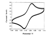
- Example Compound A-1 which is an organic compound of the present invention was subjected to 4-continuous insertion evaluation of 1-electron oxidation using cyclic voltammetry (CV).
- the CV measurement result of Example Compound A-1 is shown in FIG. 1A.
- a reversible oxidation wave was obtained as a result of CV measurement of Example Compound A-1, almost no change in the waveform, and almost no deterioration of Example Compound A-1 due to repeated insertion. There wasn't. This indicates that Exemplified Compound A-1 can exist stably without causing decomposition or reaction due to one-electron oxidation.
- Comparative compound R-2 has a high activity of proton at the ⁇ -position of the thiophene moiety shown below by directly bonding an amino group having higher electron donating property to thiophene having higher electron donating property, and the electrophilic substitution reaction is activated. It is thought that.
- the CV measurement was carried out in a 0.1 M tetrabutylammonium perchlorate ortho-dichlorobenzene solution, using Ag / Ag + for the reference electrode, Pt for the counter electrode, and glassy carbon for the working electrode. Further, the insertion speed was 0.1 V / s.
- As a measuring device model 660C manufactured by ALS, an electrochemical analyzer was used.
- the organic compound of the present invention has high stability against redox reaction and is effective in durability against repeated use of the organic photoelectric conversion element.
- the organic compound layer is preferably produced by a vacuum deposition method. Other methods such as a coating process are also possible.
- a high-purity organic compound layer can be formed by using a vacuum evaporation method.
- an organic photoelectric conversion compound is so preferable that it is high purity.
- the organic compound of the present invention is stable without being decomposed during vacuum deposition or sublimation purification.
- Exemplified Compound A-1 was purified by sublimation at 270 ° C.
- Comparative Compound R-2 decomposed at 280 ° C. without sublimation. This also indicates that the comparative compound R-2 is decomposed during the vacuum deposition and cannot be used in the vacuum deposition process.
- the organic compound of the present invention has high thermal stability and does not decompose in the vacuum deposition process, and can stably produce an organic compound layer.
- the comparative compound R-2 has a high ⁇ -position proton activity due to its high electron donating property and the decomposition reaction is activated, similarly to the reason that the stability to the redox reaction described in (2) is low. Conceivable.
- the organic compound of the present invention Since the organic compound of the present invention has the characteristics shown in the above (1) to (3), it has good panchromic performance, high molar extinction coefficient, high redox stability, and thermal stability. In particular, it can be provided as a compound having high deposition stability. Therefore, the organic compound of the present invention exhibits high vapor deposition stability in the production of the organic photoelectric conversion film and the organic photoelectric conversion element, and is visible when used as a compound layer of the organic photoelectric conversion film and the organic photoelectric conversion element. Good photoelectric conversion characteristics can be obtained in the entire light range.
- FIG. 2 is a schematic cross-sectional view showing an example of the organic photoelectric conversion element of the present invention.
- a first organic compound layer 1 that is a photoelectric conversion unit that converts light into electric charge is disposed between a hole collection electrode 4 and an electron collection electrode 5.
- the first organic compound layer 1 is a layer that receives light and generates a charge corresponding to the amount of light. It can also be called a photoelectric conversion layer because of its function.
- the first organic compound layer 1 has at least the organic compound of the present invention.
- the first organic compound layer 1 may have a plurality of types of organic compounds.
- the first organic compound layer 1 has a plurality of types of organic compounds
- a plurality of types of organic compounds may be mixed in one layer, or a plurality of types of organic compounds may be included in a plurality of layers.
- the plurality of layers are preferably stacked in the direction from the electron collection electrode 5 to the hole collection electrode 4.
- the electron collecting electrode 5 is also called an anode
- the hole collecting electrode 4 is also called a cathode.
- the first organic compound layer 1 is preferably a layer containing an organic p-type semiconductor or an organic n-type semiconductor, and a bulk hetero layer (mixed layer) in which an organic p-type compound and an organic n-type compound are mixed. It is more preferable that at least a part thereof is contained.
- photoelectric conversion efficiency sensitivity
- the first organic compound layer 1 preferably contains fullerene or a fullerene derivative as an organic n-type semiconductor. Since the fullerene or fullerene derivative is continuous in the first organic compound layer 1, an electron path is formed, so that the electron transport property is improved and the high-speed response of the organic photoelectric conversion element is improved.
- the content of fullerene or fullerene derivative is preferably 40% by volume or more and 85% by volume or less with respect to the volume of the first organic compound layer 1.
- fullerenes include fullerene C60, fullerene C70, fullerene C76, fullerene C78, fullerene C80, fullerene C82, fullerene C84, fullerene C90, fullerene C96, fullerene C240, fullerene 540, mixed fullerene, and fullerene nanotubes.
- the fullerene derivative has a substituent on the fullerene, and examples of the substituent include an alkyl group, an aryl group, and an aromatic heterocyclic group.
- the organic p-type semiconductor included in the first organic compound layer 1 is a donor-type organic semiconductor, and is an organic compound that has a property of mainly donating electrons typified by a hole-transporting organic compound.
- the organic photoelectric conversion element of the present invention contains the organic compound of the present invention as an organic p-type semiconductor (electron donor compound).
- the first organic compound layer 1 preferably does not emit light.
- Non-light-emitting means a layer having an emission quantum efficiency of 1% or less, preferably 0.5% or less, more preferably 0.1% or less in the visible light region (wavelength 400 nm to 730 nm).
- the light emission quantum efficiency is 1% or less without affecting the sensing performance or the imaging performance when applied to a sensor or an imaging device.
- the second organic compound layer 2 is a layer that suppresses the flow of electrons from the hole collection electrode 4 to the first organic compound layer 1, and can also be referred to as an electron blocking layer.
- the unoccupied orbit energy is preferably small.
- the organic photoelectric conversion element of the present invention does not necessarily have the second organic compound layer 2.
- the third organic compound layer 3 is a layer that suppresses the flow of holes from the electron collection electrode 5 to the first organic compound layer 1, and can also be referred to as a hole blocking layer, and has a high ionization potential. Is preferred.
- the organic photoelectric conversion element of the present invention does not necessarily have to include the third organic compound layer 3.
- the hole collection electrode 4 is an electrode that collects holes out of the charges generated in the first organic compound layer 1.
- the material constituting the hole collecting electrode 4 is not limited as long as it has high conductivity and transparency. Specific examples include metals, metal oxides, metal nitrides, metal borides, organic conductive compounds, and mixtures thereof. More specifically, tin oxide doped with antimony or fluorine (ATO or FTO). ), Conductive metal oxides such as tin oxide, zinc oxide, indium oxide, indium tin oxide (ITO), indium zinc oxide (IZO), gold, silver, chromium, nickel, titanium, molybdenum, tantalum, tungsten, aluminum, etc.
- conductive compounds such as oxides and nitrides of these metals (for example, titanium nitride (TiN)), a mixture or laminate of these metals and conductive metal oxides, copper iodide, Inorganic conductive materials such as copper sulfide, organic conductive materials such as polyaniline, polythiophene and polypyrrole, and these and ITO or titanium nitride Like laminates of the like.
- the hole collecting electrode 4 is any material of titanium nitride, molybdenum nitride, tantalum nitride, and tungsten nitride.
- the electron collection electrode 5 is an electrode that collects electrons out of the charges generated in the first organic compound layer 1.
- the electron collection electrode 5 is disposed closer to the pixel circuit than the hole collection electrode 4.
- Specific examples of the material constituting the electron collecting electrode 5 include ITO, IZO, SnO 2 , ATO (antimony-doped tin oxide), ZnO, AZO (aluminum-doped zinc oxide), GZO (gallium-doped zinc oxide), and TiO. 2 or any material of FTO (fluorine-doped tin oxide).
- the method for forming the electrode can be appropriately selected in consideration of suitability with the electrode material.
- the electrode may be formed by a wet method such as a printing method or a coating method, a physical method such as a vacuum deposition method, a sputtering method or an ion plating method, or a chemical method such as CVD or plasma CVD method. it can.
- the ITO electrode can be formed by a method such as an electron beam method, a sputtering method, a resistance heating vapor deposition method, a chemical reaction method (sol-gel method or the like), or a dispersion of indium tin oxide.
- the formed ITO electrode can be subjected to UV-ozone treatment, plasma treatment, and the like.
- the electrode is TiN
- various methods including a reactive sputtering method are used, and the formed TiN electrode can be further subjected to annealing treatment, UV-ozone treatment, plasma treatment, and the like.
- the electron collection electrode 5 is connected to the readout circuit 6.
- the readout circuit 6 reads out information based on the charges generated in the organic photoelectric conversion unit composed of the first organic compound layer 1, the second organic compound layer 2, and the third organic compound layer 3, for example, a signal processing unit ( (Not shown) Further, the readout circuit 6 may be connected to the hole collecting electrode 4.
- the organic photoelectric conversion element in FIG. 2 has an inorganic protective layer 7 on the hole collecting electrode 4.
- the inorganic protective layer 7 is made of, for example, silicon oxide, silicon nitride, aluminum oxide, or the like.
- the inorganic protective layer 7 can be formed by a vacuum deposition method, a sputtering method, an atomic layer deposition (ALD) method, or the like.
- a color filter 8 is disposed on the inorganic protective layer 7.
- the color filter 8 include a color filter that transmits red light of visible light.
- one color filter 8 may be disposed for one organic photoelectric conversion element.
- one color filter 8 may be arranged for a plurality of organic photoelectric conversion elements.
- a Bayer arrangement or the like can be used as the arrangement of the color filters 8, a Bayer arrangement or the like can be used.
- a microlens 9 is disposed on the color filter 8.
- the microlens 9 can collect incident light onto the organic photoelectric conversion element.
- one microlens 9 may be arranged for one organic photoelectric conversion element. Or you may have one micro lens 9 with respect to a some organic photoelectric conversion element.
- the organic photoelectric conversion element of the present invention may have a substrate.
- the substrate include a silicon substrate, a glass substrate, and a flexible substrate.
- the organic photoelectric conversion element preferably applies a voltage between the hole collection electrode 4 and the electron collection electrode 5 when performing photoelectric conversion.
- holes may be used for reading as signal charges by reversing the hole collection and electron collection electrodes.
- the organic photoelectric conversion element according to the present invention can be an organic photoelectric conversion element having a different wavelength of received light by appropriately setting the constituent material of the first organic compound layer 1.
- the difference in the wavelength of the received light means that the wavelength range of the light that is photoelectrically converted by the photoelectric conversion unit is different.
- it can also be set as the organic photoelectric conversion apparatus which does not require the color filter 8 by having several organic photoelectric conversion elements from which the wavelength of the light which each receives differs, and laminating
- a plurality of types of organic photoelectric conversion elements included in the organic photoelectric conversion device at least one type of organic photoelectric conversion element is the organic photoelectric conversion element of the present invention.
- the optical area sensor of the present invention has a plurality of photoelectric conversion elements.
- the plurality of photoelectric conversion elements are two-dimensionally arranged in the in-plane direction. In such a configuration, information representing the light intensity distribution in a predetermined light receiving area can be obtained by individually outputting signals based on the charges generated in the plurality of organic photoelectric conversion elements.
- the optical area sensor may have the above-described organic photoelectric conversion device of the present invention instead of the organic photoelectric conversion element of the present invention.
- the image sensor of the present invention has a plurality of organic photoelectric conversion elements each serving as a light receiving pixel, and a transistor connected to each organic photoelectric conversion element.
- the transistor reads the charge generated in the organic photoelectric conversion element, and transmits information based on the read charge to the sensor unit connected to the imaging element.
- Examples of the sensor unit include a CMOS sensor and a CCD sensor. An image can be obtained by collecting the information acquired by each light receiving pixel in the sensor unit.
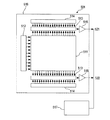
- FIG. 3 is a schematic diagram showing an example of the image sensor of the present invention.
- the imaging device 501 includes an imaging region 511, a vertical scanning circuit 512, two readout circuits 513, two horizontal scanning circuits 514, and two output amplifiers 515.
- An area other than the imaging area 511 is a circuit area 516.
- the imaging region 511 is configured by arranging a plurality of light receiving pixels in a two-dimensional manner.
- the read circuit 513 includes, for example, a column amplifier, a CDS circuit, an adder circuit, and the like, and amplifies and adds signals read from the pixels in the row selected by the vertical scanning circuit 512 via the vertical signal line. Do.
- the column amplifier, the CDS circuit, the adder circuit, and the like are arranged for each pixel column or a plurality of pixel columns, for example.
- the horizontal scanning circuit 514 generates a signal for sequentially reading the signals of the reading circuit 513.
- the output amplifier 515 amplifies and outputs the signal of the column selected by the horizontal scanning circuit 514.
- the readout circuit 513, the horizontal scanning circuit 514, and the output amplifier 515 are arranged one above the other with the imaging region 511 interposed therebetween in order to configure two output paths. However, three or more output paths may be provided.
- the output signal 521 and the output signal 522 output from each output amplifier 515 are combined as an image signal by the signal processing unit 517.
- FIG. 4 is an example of a pixel drive circuit diagram for driving the light receiving pixels of the image sensor 501.
- the light receiving pixel 100 includes an organic photoelectric conversion element 101.
- the lower surface of the semiconductor layer of the first organic compound layer 1 of the organic photoelectric conversion element 101 is electrically connected to the charge storage unit 115 in the semiconductor substrate and further connected to the amplification unit 103.
- the charge accumulation unit 115 in the Si semiconductor substrate is a region for accumulating charges generated in the organic photoelectric conversion element 101, and a P-type region and an N-type region may be formed.
- the amplification unit 103 can output a signal generated in the organic photoelectric conversion element 101.
- the organic photoelectric conversion element 101 and the amplification unit 103 may be short-circuited.
- FIG. 4 illustrates a node B122 representing the electrical connection between the organic photoelectric conversion element 101 and the amplification unit 103.
- Node B 122 is configured to be electrically floating. When the node B122 is electrically floating, the voltage of the node B122 can be changed according to the electric charge generated in the organic photoelectric conversion element 101. Therefore, a signal corresponding to the charge generated in the organic photoelectric conversion element 101 can be input to the amplification unit 103.
- the light receiving pixel 100 in FIG. 4 includes a reset unit 102 that resets the voltage of the node B122 in the semiconductor substrate.
- the reset unit 102 supplies a reset voltage (not shown) to the node B122.
- the reset unit 102 is, for example, a reset transistor electrically connected to the node B122.
- FIG. 4 illustrates a reset transistor.
- the reset unit 102 is controlled to be switched on and off by a reset control pulse (pRES) 124. When the reset unit 102 is turned on, a reset voltage is supplied to the node B122.
- pRES reset control pulse
- 121 is a common wiring connection (node A)
- 130 is an output line
- 140 is a column circuit
- 160 is a current source
- 104 is a selection transistor for selectively sending a signal to the output line 130.
- the selection transistor 104 is controlled to be switched on and off by a selection transistor drive signal (pSEL) 125.
- the image sensor may have an optical filter such as a color filter.
- an optical filter such as a color filter.
- One optical filter may be provided for one light receiving pixel, or one optical filter may be provided for a plurality of light receiving pixels. Examples of the optical filter include a color filter, a long-pass filter that transmits wavelengths of infrared rays or more, a UV cut filter that transmits wavelengths of ultraviolet rays or less, and a low-pass filter.
- the image sensor may have an optical member such as a microlens.
- the microlens is a lens that collects light from the outside onto the photoelectric conversion unit.
- one optical member may be provided for one light receiving pixel, or one optical member corresponding to a plurality of light receiving pixels may be provided. When a plurality of light receiving pixels are provided, it is preferable that one optical member is provided for each of the plurality of light receiving pixels.
- the imaging apparatus of the present invention includes an imaging optical system having a plurality of lenses and an imaging element that receives light that has passed through the imaging optical system.
- the imaging device may be an imaging device having a joint portion that can be joined to the imaging optical system and an imaging element. More specifically, the imaging device is a digital camera or a digital still camera.
- the imaging device may further include a receiving unit that receives an external signal. The signal received by the receiving unit is a signal that controls at least one of the imaging range of the imaging device, the start of imaging, and the end of imaging.
- the imaging device may further include a transmission unit that transmits the captured image to the outside. By having a receiving unit and a transmitting unit, it can be used as a network camera.
- Examples 4 to 10> In the same manner as in Example 1, except that c-1, c-2, and c-4 were replaced with tertiary amine halides, thiophene boronic acids, and indane derivatives shown in Table 2, respectively, the exemplified compounds shown in Table 2 was synthesized.
- Examples 11 to 19 and Comparative Examples 1 to 3 The compounds d-1 to d-3 used in Examples and Comparative Examples are shown below.
- the compounds R-1 and R-2 used in the comparative examples are the compound R-1 described in Non-Patent Document 1 and the compound R-2 described in Patent Document 1.
- a hole collection electrode 4 On the substrate, a hole collection electrode 4, an electron blocking layer (second organic compound layer 2), a photoelectric conversion layer (first organic compound layer 1), a hole blocking layer (third organic compound layer 3). ) And the electron collecting electrode 5 were produced by the method described below.
- an indium tin oxide film was formed on a Si substrate, and a hole patterning electrode 4 was formed by performing a desired patterning process. At this time, the thickness of the hole collecting electrode 4 was set to 100 nm. Thus, the board
- the organic compound layers 1 to 3 and the electron collecting electrode 5 shown in Table 3 were continuously formed.
- Organic compound layers 1 to 3 were formed by vacuum deposition.
- the exemplified compound A-1 is used as the electron donor material
- the compound d-3 is used as the electron acceptor compound
- the exemplified compound A-1: compound d-3 is in a volume ratio of 25:75. It vapor-deposited like.
- the electrode area of the electron collection electrode 5 facing the hole collection electrode 4 was set to 3 mm 2 . This obtained the organic photoelectric conversion element.
- Example 12 to 19 Comparative Examples 1 to 3
- An organic photoelectric conversion element was obtained by the same method as in Example 11 except that the electron donor material in the first organic compound layer 1 and the material of the second organic compound layer 2 were changed as shown in Table 4. .
- the monochromatic light used for the measurement of the photocurrent density is white light emitted from a xenon lamp (device name: XB-50101AA-A, manufactured by USHIO), a monochromator (device name: MC-10N, It is a monochromatic product made by Ritu Applied Optics). Voltage application to the element and current measurement were performed using a source meter (device name: R6243, manufactured by Advantest). Further, in the measurement of the light absorption rate and the external quantum efficiency inside the device, light was incident perpendicularly to the device and from the upper electrode (electron collecting electrode 5) side.
- the external quantum efficiency at a wavelength of 600 nm of the organic photoelectric conversion elements of Examples 12 to 19 and Comparative Examples 1 to 3 was evaluated according to the following criteria.
- a relative value is a relative value when the external quantum efficiency in wavelength 600nm of the organic photoelectric conversion element of Example 11 is set to 1.
- the results are shown in Table 4.
- the organic compound of the present invention can be produced without decomposing at the time of vapor deposition, and the produced organic photoelectric conversion element is sensitive in the visible light region on the long wavelength side of 600 nm. I understood.
Landscapes
- Chemical & Material Sciences (AREA)
- Organic Chemistry (AREA)
- Physics & Mathematics (AREA)
- Engineering & Computer Science (AREA)
- Materials Engineering (AREA)
- Spectroscopy & Molecular Physics (AREA)
- Electromagnetism (AREA)
- Nanotechnology (AREA)
- Light Receiving Elements (AREA)
- Solid State Image Pick-Up Elements (AREA)
- Electroluminescent Light Sources (AREA)
- Plural Heterocyclic Compounds (AREA)
Priority Applications (1)
| Application Number | Priority Date | Filing Date | Title |
|---|---|---|---|
| US16/243,500 US10978644B2 (en) | 2016-07-21 | 2019-01-09 | Organic compound and organic photoelectric conversion element including the same |
Applications Claiming Priority (2)
| Application Number | Priority Date | Filing Date | Title |
|---|---|---|---|
| JP2016143317A JP2018014426A (ja) | 2016-07-21 | 2016-07-21 | 有機化合物及びそれを有する有機光電変換素子 |
| JP2016-143317 | 2016-07-21 |
Related Child Applications (1)
| Application Number | Title | Priority Date | Filing Date |
|---|---|---|---|
| US16/243,500 Continuation US10978644B2 (en) | 2016-07-21 | 2019-01-09 | Organic compound and organic photoelectric conversion element including the same |
Publications (1)
| Publication Number | Publication Date |
|---|---|
| WO2018016354A1 true WO2018016354A1 (ja) | 2018-01-25 |
Family
ID=60992970
Family Applications (1)
| Application Number | Title | Priority Date | Filing Date |
|---|---|---|---|
| PCT/JP2017/024986 Ceased WO2018016354A1 (ja) | 2016-07-21 | 2017-07-07 | 有機化合物及びそれを有する有機光電変換素子 |
Country Status (3)
| Country | Link |
|---|---|
| US (1) | US10978644B2 (https=) |
| JP (2) | JP2018014426A (https=) |
| WO (1) | WO2018016354A1 (https=) |
Cited By (6)
| Publication number | Priority date | Publication date | Assignee | Title |
|---|---|---|---|---|
| US10861903B2 (en) | 2017-08-07 | 2020-12-08 | Canon Kabushiki Kaisha | Organic compound and photoelectric conversion element |
| US10868260B2 (en) | 2017-09-20 | 2020-12-15 | Canon Kabushiki Kaisha | Organic compound and photoelectric conversion element |
| US10873032B2 (en) | 2016-03-03 | 2020-12-22 | Canon Kabushiki Kaisha | Organic photoelectric conversion element, two-dimensional sensor, image sensor, and imaging apparatus |
| US10978644B2 (en) | 2016-07-21 | 2021-04-13 | Canon Kabushiki Kaisha | Organic compound and organic photoelectric conversion element including the same |
| US11555028B2 (en) | 2017-10-25 | 2023-01-17 | Canon Kabushiki Kaisha | Organic compound and photoelectric conversion element |
| US11895910B2 (en) | 2017-08-23 | 2024-02-06 | Canon Kabushiki Kaisha | Organic compound and photoelectric conversion element |
Families Citing this family (3)
| Publication number | Priority date | Publication date | Assignee | Title |
|---|---|---|---|---|
| EP3582275B1 (en) | 2017-02-07 | 2023-09-06 | Canon Kabushiki Kaisha | Photoelectric conversion element, optical area sensor using same, imaging element, and imaging device |
| JP2023118407A (ja) | 2022-02-15 | 2023-08-25 | 日本トムソン株式会社 | 直動案内ユニット |
| CN116803994A (zh) * | 2023-06-26 | 2023-09-26 | 厦门大学 | 化合物、其立体异构体或光学异构体及制备方法、给体材料、太阳能电池、用电装置及应用 |
Citations (12)
| Publication number | Priority date | Publication date | Assignee | Title |
|---|---|---|---|---|
| JP2003238559A (ja) * | 2002-02-08 | 2003-08-27 | Mitsui Chemicals Inc | アミン化合物 |
| JP2005008558A (ja) * | 2003-06-19 | 2005-01-13 | Mitsui Chemicals Inc | 五員環化合物、および該五員環化合物を含有する有機電界発光素子 |
| JP2006063043A (ja) * | 2004-08-30 | 2006-03-09 | Mitsui Chemicals Inc | アミノ置換テトラフェニルチオフェン化合物、および該化合物を含有する有機電界発光素子 |
| JP2007091714A (ja) * | 2005-09-27 | 2007-04-12 | Samsung Electronics Co Ltd | 新規な窒素系半導体化合物並びにこれを用いた有機薄膜トランジスタ、有機太陽光電池および有機電界発光素子 |
| JP2007201408A (ja) * | 2005-12-26 | 2007-08-09 | Fuji Xerox Co Ltd | 有機電界発光素子 |
| JP2009079092A (ja) * | 2007-09-25 | 2009-04-16 | Mitsui Chemicals Inc | 高分子化合物、および該高分子化合物を含有する有機電界発光素子 |
| CN101787020A (zh) * | 2010-03-24 | 2010-07-28 | 吉林大学 | 一种可溶液加工的有机共轭分子及在太阳能电池中的应用 |
| JP2011500882A (ja) * | 2007-10-15 | 2011-01-06 | 東進セミケム株式会社 | 新規なチオフェン系染料及びその製造方法 |
| CN101962380A (zh) * | 2010-09-13 | 2011-02-02 | 吉林大学 | 一种新型有机共轭分子及其在有机太阳能电池中的应用 |
| JP2012051854A (ja) * | 2010-09-03 | 2012-03-15 | Toyo Ink Sc Holdings Co Ltd | インダノン誘導体とその色素増感型太陽電池用色材としての利用 |
| WO2013168084A1 (de) * | 2012-05-10 | 2013-11-14 | Heliatek Gmbh | Optoelektronische baulemente mit organischem lochtransportmaterial |
| WO2016066494A1 (en) * | 2014-10-31 | 2016-05-06 | Basf Se | Hole-transport materials for organic solar cells or organic optical sensors |
Family Cites Families (11)
| Publication number | Priority date | Publication date | Assignee | Title |
|---|---|---|---|---|
| US20060119724A1 (en) * | 2004-12-02 | 2006-06-08 | Fuji Photo Film Co., Ltd. | Imaging device, signal processing method on solid-state imaging element, digital camera and controlling method therefor and color image data generating method |
| JP5217475B2 (ja) * | 2008-02-07 | 2013-06-19 | コニカミノルタビジネステクノロジーズ株式会社 | 光電変換素子及び太陽電池 |
| JP2009269987A (ja) * | 2008-05-07 | 2009-11-19 | Konica Minolta Business Technologies Inc | 新規化合物、光電変換素子及び太陽電池 |
| KR101772227B1 (ko) * | 2009-09-08 | 2017-08-28 | 후지필름 가부시키가이샤 | 광전 변환 재료, 그 재료를 함유하는 필름, 광전 변환 소자, 그 제조 방법, 광센서, 촬상 소자 및 그들의 사용 방법 |
| JP5520560B2 (ja) | 2009-09-29 | 2014-06-11 | 富士フイルム株式会社 | 光電変換素子、光電変換素子材料、光センサ、及び撮像素子 |
| JP2015065267A (ja) * | 2013-09-25 | 2015-04-09 | 東洋インキScホールディングス株式会社 | 有機薄膜太陽電池素子用材料およびその用途 |
| JP6206037B2 (ja) * | 2013-09-26 | 2017-10-04 | 株式会社リコー | 光電変換素子 |
| JP6777983B2 (ja) * | 2014-11-04 | 2020-10-28 | 三星電子株式会社Samsung Electronics Co.,Ltd. | 有機光電素子用化合物及びこれを含む有機光電素子並びにイメージセンサー及び電子装置 |
| WO2016190217A1 (ja) * | 2015-05-28 | 2016-12-01 | ソニーセミコンダクタソリューションズ株式会社 | 光電変換素子および固体撮像装置ならびに電子機器 |
| JP6645700B2 (ja) | 2016-03-03 | 2020-02-14 | キヤノン株式会社 | 有機光電変換素子、二次元センサ、画像センサ及び撮像装置 |
| JP2018014426A (ja) | 2016-07-21 | 2018-01-25 | キヤノン株式会社 | 有機化合物及びそれを有する有機光電変換素子 |
-
2016
- 2016-07-21 JP JP2016143317A patent/JP2018014426A/ja active Pending
-
2017
- 2017-07-07 WO PCT/JP2017/024986 patent/WO2018016354A1/ja not_active Ceased
-
2019
- 2019-01-09 US US16/243,500 patent/US10978644B2/en active Active
-
2021
- 2021-11-04 JP JP2021179948A patent/JP7379444B2/ja active Active
Patent Citations (12)
| Publication number | Priority date | Publication date | Assignee | Title |
|---|---|---|---|---|
| JP2003238559A (ja) * | 2002-02-08 | 2003-08-27 | Mitsui Chemicals Inc | アミン化合物 |
| JP2005008558A (ja) * | 2003-06-19 | 2005-01-13 | Mitsui Chemicals Inc | 五員環化合物、および該五員環化合物を含有する有機電界発光素子 |
| JP2006063043A (ja) * | 2004-08-30 | 2006-03-09 | Mitsui Chemicals Inc | アミノ置換テトラフェニルチオフェン化合物、および該化合物を含有する有機電界発光素子 |
| JP2007091714A (ja) * | 2005-09-27 | 2007-04-12 | Samsung Electronics Co Ltd | 新規な窒素系半導体化合物並びにこれを用いた有機薄膜トランジスタ、有機太陽光電池および有機電界発光素子 |
| JP2007201408A (ja) * | 2005-12-26 | 2007-08-09 | Fuji Xerox Co Ltd | 有機電界発光素子 |
| JP2009079092A (ja) * | 2007-09-25 | 2009-04-16 | Mitsui Chemicals Inc | 高分子化合物、および該高分子化合物を含有する有機電界発光素子 |
| JP2011500882A (ja) * | 2007-10-15 | 2011-01-06 | 東進セミケム株式会社 | 新規なチオフェン系染料及びその製造方法 |
| CN101787020A (zh) * | 2010-03-24 | 2010-07-28 | 吉林大学 | 一种可溶液加工的有机共轭分子及在太阳能电池中的应用 |
| JP2012051854A (ja) * | 2010-09-03 | 2012-03-15 | Toyo Ink Sc Holdings Co Ltd | インダノン誘導体とその色素増感型太陽電池用色材としての利用 |
| CN101962380A (zh) * | 2010-09-13 | 2011-02-02 | 吉林大学 | 一种新型有机共轭分子及其在有机太阳能电池中的应用 |
| WO2013168084A1 (de) * | 2012-05-10 | 2013-11-14 | Heliatek Gmbh | Optoelektronische baulemente mit organischem lochtransportmaterial |
| WO2016066494A1 (en) * | 2014-10-31 | 2016-05-06 | Basf Se | Hole-transport materials for organic solar cells or organic optical sensors |
Non-Patent Citations (5)
| Title |
|---|
| GUPTA AKHIL ET AL.: "Molecular engineering for panchromatic absorbing oligothiophene donor-pi-acceptor organic semiconductors", TETRAHEDRON, vol. 68, no. 46, 2012, pages 9440 - 9447, XP028943858, ISSN: 0040-4020, DOI: 10.1016/j.tet.2012.09.009 * |
| HIRADE MASAYA ET AL.: "Effects of Intramolecular Donor-Acceptor Interactions on Bimolecular Recombination in Small-Molecule Organic Photovoltaic Cells", JOURNAL OF PHYSICAL CHEMISTRY C, vol. 117, no. 10, 2013, pages 4986 - 4991, XP055602451, ISSN: 1932-7447, DOI: 10.1021/jp400386q * |
| LERICHE PHILIPPE ET AL.: "Molecular Engineering of the Inter nal Charge Transfer in Thiophene-Triphenylamine Hybrid pi'Co njugated Systems", JOURNAL OF ORGANIC CHEMISTRY, vol. 72, no. 22, October 2007 (2007-10-01), pages 8332 - 8336, XP055446969, ISSN: 0022-3263, DOI: 10.1021/jo701390y * |
| QI CHUNXUAN ET AL.: "Study of Red-Emission Piezochromic Mate rials Based on Triphenylamine", CHEMPLUSCHEM, vol. 81, no. 7, 25 May 2016 (2016-05-25) - 17 June 2016 (2016-06-17), pages 637 - 645, XP055602447, ISSN: 2192-6506, DOI: 10.1002/cplu.201600104 * |
| ROQUET SOPHIE ET AL.: "Triphenylamine-Thienylenevinylene Hybrid Systems with Internal Charge Transfer as Donor Materials for Heterojunction Solar Cells", JOURNAL OF THE AMERICAN CHE MICAL SOCIETY, vol. 128, no. 10, 2006, pages 3459 - 3466, XP002397900, ISSN: 0002-7863, DOI: 10.1021/ja058178e * |
Cited By (7)
| Publication number | Priority date | Publication date | Assignee | Title |
|---|---|---|---|---|
| US10873032B2 (en) | 2016-03-03 | 2020-12-22 | Canon Kabushiki Kaisha | Organic photoelectric conversion element, two-dimensional sensor, image sensor, and imaging apparatus |
| US10978644B2 (en) | 2016-07-21 | 2021-04-13 | Canon Kabushiki Kaisha | Organic compound and organic photoelectric conversion element including the same |
| US10861903B2 (en) | 2017-08-07 | 2020-12-08 | Canon Kabushiki Kaisha | Organic compound and photoelectric conversion element |
| US11895910B2 (en) | 2017-08-23 | 2024-02-06 | Canon Kabushiki Kaisha | Organic compound and photoelectric conversion element |
| US10868260B2 (en) | 2017-09-20 | 2020-12-15 | Canon Kabushiki Kaisha | Organic compound and photoelectric conversion element |
| US11793074B2 (en) | 2017-09-20 | 2023-10-17 | Canon Kabushiki Kaisha | Organic compound and photoelectric conversion element |
| US11555028B2 (en) | 2017-10-25 | 2023-01-17 | Canon Kabushiki Kaisha | Organic compound and photoelectric conversion element |
Also Published As
| Publication number | Publication date |
|---|---|
| JP2018014426A (ja) | 2018-01-25 |
| JP7379444B2 (ja) | 2023-11-14 |
| JP2022021347A (ja) | 2022-02-02 |
| US10978644B2 (en) | 2021-04-13 |
| US20190148644A1 (en) | 2019-05-16 |
Similar Documents
| Publication | Publication Date | Title |
|---|---|---|
| JP7379444B2 (ja) | 有機化合物及び有機光電変換素子 | |
| JP6645700B2 (ja) | 有機光電変換素子、二次元センサ、画像センサ及び撮像装置 | |
| JP7433741B2 (ja) | 光電変換素子、二次元センサ、画像センサおよび撮像装置 | |
| JP6833351B2 (ja) | 有機光電変換素子、光エリアセンサ、撮像素子および撮像装置 | |
| JP6029606B2 (ja) | 光電変換素子、撮像素子、光センサ、光電変換素子の使用方法 | |
| KR20110028234A (ko) | 광전 변환 소자 및 그 제조방법, 광센서, 촬상소자 및 이들의 구동방법 | |
| JP7013163B2 (ja) | 有機化合物及び光電変換素子 | |
| JP6932564B2 (ja) | 有機光電変換素子、撮像素子及び撮像装置 | |
| JP7051332B2 (ja) | 有機化合物及び光電変換素子 | |
| JP7791700B2 (ja) | インドロカルバゾール環を有する化合物、受光素子用材料、有機薄膜、受光素子、及び撮像素子 | |
| JP2019055919A (ja) | 有機化合物及び光電変換素子 | |
| JP7016662B2 (ja) | 有機化合物、それを用いた光電変換素子および撮像装置 | |
| WO2022181439A1 (ja) | ホウ素キレート化合物、近赤外光吸収材料、薄膜、光電変換素子、及び撮像素子 | |
| JP7177001B2 (ja) | ジベンゾピロメテンホウ素キレート化合物、近赤外光吸収色素、光電変換素子、近赤外光センサー及び撮像素子 | |
| JP7177002B2 (ja) | ジベンゾピロメテンホウ素キレート化合物、近赤外光吸収色素、光電変換素子、近赤外光センサー及び撮像素子 | |
| JP2017034112A (ja) | 近赤外光電変換素子、光センサ及び近赤外光電変換素子用材料 | |
| KR102939714B1 (ko) | 광전 변환 소자에 사용하는 유기 박막 및 그 광전 변환 소자 | |
| JP2022081515A (ja) | 光電変換素子、二次元センサ、画像センサおよび撮像装置 | |
| WO2024062997A1 (ja) | 化合物、有機薄膜および光電変換素子 | |
| TWI611594B (zh) | 光電轉換元件、攝影元件、光感測器 |
Legal Events
| Date | Code | Title | Description |
|---|---|---|---|
| 121 | Ep: the epo has been informed by wipo that ep was designated in this application |
Ref document number: 17830874 Country of ref document: EP Kind code of ref document: A1 |
|
| NENP | Non-entry into the national phase |
Ref country code: DE |
|
| 122 | Ep: pct application non-entry in european phase |
Ref document number: 17830874 Country of ref document: EP Kind code of ref document: A1 |